JP2006248093A - Patterning method and manufacturing method for liquid jet head - Google Patents
Patterning method and manufacturing method for liquid jet head Download PDFInfo
- Publication number
- JP2006248093A JP2006248093A JP2005069552A JP2005069552A JP2006248093A JP 2006248093 A JP2006248093 A JP 2006248093A JP 2005069552 A JP2005069552 A JP 2005069552A JP 2005069552 A JP2005069552 A JP 2005069552A JP 2006248093 A JP2006248093 A JP 2006248093A
- Authority
- JP
- Japan
- Prior art keywords
- metal film
- metal
- film
- patterning
- flow path
- Prior art date
- Legal status (The legal status is an assumption and is not a legal conclusion. Google has not performed a legal analysis and makes no representation as to the accuracy of the status listed.)
- Withdrawn
Links
Images


Landscapes
- Particle Formation And Scattering Control In Inkjet Printers (AREA)
Abstract
Description
本発明は、金属材料からなる金属膜を所定形状にパターニングするためのパターニング方法に関し、特に、インク滴を吐出するノズル開口と連通する圧力発生室の一部を振動板で構成し、この振動板の表面に圧電素子を形成して、圧電素子の変位によりインク滴を吐出させるインクジェット式記録ヘッド等の液体噴射ヘッドの製造方法に用いるのに好適なものである。 The present invention relates to a patterning method for patterning a metal film made of a metal material into a predetermined shape, and in particular, a part of a pressure generating chamber communicating with a nozzle opening for ejecting ink droplets is constituted by a diaphragm, and the diaphragm This is suitable for use in a method of manufacturing a liquid ejecting head such as an ink jet recording head in which a piezoelectric element is formed on the surface of the ink jet and ink droplets are ejected by displacement of the piezoelectric element.
液体噴射ヘッドの代表例としては、例えば、インク滴を吐出するノズル開口と連通する圧力発生室の一部を振動板で構成し、この振動板を圧電素子により変形させて圧力発生室のインクを加圧してノズル開口からインク滴を吐出させるインクジェット式記録ヘッドがある。また、インクジェット式記録ヘッドには、圧電素子の軸方向に伸長、収縮する縦振動モードの圧電アクチュエータを使用したものと、たわみ振動モードの圧電アクチュエータを使用したものの2種類が実用化されている。前者は圧電素子の端面を振動板に当接させることにより圧力発生室の容積を変化させることができて、高密度印刷に適したヘッドの製作が可能である反面、圧電素子をノズル開口の配列ピッチに一致させて櫛歯状に切り分けるという困難な工程や、切り分けられた圧電素子を圧力発生室に位置決めして固定する作業が必要となり、製造工程が複雑であるという問題がある。これに対して後者は、圧電材料のグリーンシートを圧力発生室の形状に合わせて貼付し、これを焼成するという比較的簡単な工程で振動板に圧電素子を作り付けることができるものの、たわみ振動を利用する関係上、ある程度の面積が必要となり、高密度配列が困難であるという問題がある。 As a typical example of a liquid ejecting head, for example, a part of a pressure generation chamber communicating with a nozzle opening for ejecting ink droplets is configured by a vibration plate, and the vibration plate is deformed by a piezoelectric element so that the ink in the pressure generation chamber is There is an ink jet recording head that pressurizes and ejects ink droplets from nozzle openings. Two types of ink jet recording heads have been put into practical use: those using a longitudinal vibration mode piezoelectric actuator that expands and contracts in the axial direction of the piezoelectric element, and those using a flexural vibration mode piezoelectric actuator. The former can change the volume of the pressure generation chamber by bringing the end face of the piezoelectric element into contact with the diaphragm, and it is possible to manufacture a head suitable for high-density printing, while the piezoelectric element is arranged in an array of nozzle openings. There is a problem that the manufacturing process is complicated because a difficult process of matching the pitch into a comb-like shape and an operation of positioning and fixing the cut piezoelectric element in the pressure generating chamber are necessary. On the other hand, the latter can flexibly vibrate, although a piezoelectric element can be built on the diaphragm by a relatively simple process of sticking a green sheet of piezoelectric material according to the shape of the pressure generation chamber and firing it. There is a problem that a certain amount of area is required for the use of, and high-density arrangement is difficult.
このような後者の記録ヘッドの不都合を解消すべく、振動板の表面全体に亙って成膜技術により均一な圧電材料層を形成し、この圧電材料層をリソグラフィ法により圧力発生室に対応する形状に切り分けて各圧力発生室毎に独立するように圧電素子を形成したものがある。これによれば圧電素子を振動板に貼付ける作業が不要となって、リソグラフィ法という精密で、かつ簡便な手法で圧電素子を高密度に作り付けることができるばかりでなく、圧電素子の厚みを薄くできて高速駆動が可能になるという利点がある。 In order to eliminate the disadvantages of the latter recording head, a uniform piezoelectric material layer is formed over the entire surface of the diaphragm by a film forming technique, and this piezoelectric material layer corresponds to the pressure generating chamber by lithography. There is one in which piezoelectric elements are formed so as to be separated into shapes and independent for each pressure generating chamber. This eliminates the need to affix the piezoelectric element to the diaphragm, and not only enables the piezoelectric element to be densely formed by a precise and simple technique called lithography, but also reduces the thickness of the piezoelectric element. There is an advantage that it can be made thin and can be driven at high speed.
また、このようなインクジェット式記録ヘッドには、例えば、圧力発生室が形成される流路形成基板に接合された接合基板上に配線パターンを介して圧電素子を駆動するための駆動ICが実装されたものがある(例えば、特許文献1参照)。 Also, in such an ink jet recording head, for example, a driving IC for driving a piezoelectric element via a wiring pattern is mounted on a bonded substrate bonded to a flow path forming substrate in which a pressure generating chamber is formed. (See, for example, Patent Document 1).
そして、上述したような圧電素子を高密度に配列しようとすると、それに伴って、当然ながら配線数も多くなる。このため、保護基板上に形成する配線パターンも比較的狭いピッチで高密度に形成する必要がある。すなわち、配線パターンとなる金属膜を高精度にエッチングする必要があるが、現状では十分に対応できてない。特に、配線パターンを構成する金属膜の材料として比較的イオン化傾向の高い材料を用いる場合には、ウェットエッチングによって高精度にパターニングするのが難しい。イオン化傾向の高い材料からなる金属膜の表面は、自然酸化、乾燥等によって不動態化した不動態膜が形成されやすく、この不動態膜をウェットエッチングによって除去するためには、硝酸や塩酸等の濃度の濃いエッチング液を高い温度で用いる必要がある。そして、このような酸の強いエッチング液で金属膜をエッチングすれば、表面が不動態化された膜であってもパターニングすることはできるが、サイドエッチング量が大きくなる、あるいはレジスト膜が浸食されて金属膜全体の厚さが減少する等の問題が生じてしまう。また、高い処理温度でエッチング液を使用するため、エッチング液の劣化が非常に早く、有害なガス等が発生するという問題もある。 If the piezoelectric elements as described above are arranged at high density, the number of wires naturally increases accordingly. For this reason, it is necessary to form wiring patterns formed on the protective substrate with a relatively narrow pitch and high density. That is, it is necessary to etch the metal film to be a wiring pattern with high accuracy, but at present, this is not sufficient. In particular, when a material having a relatively high ionization tendency is used as the material of the metal film constituting the wiring pattern, it is difficult to pattern with high accuracy by wet etching. The surface of a metal film made of a material having a high ionization tendency is likely to form a passivated film that has been passivated by natural oxidation, drying, etc. In order to remove this passivated film by wet etching, nitric acid, hydrochloric acid, etc. It is necessary to use an etching solution having a high concentration at a high temperature. If the metal film is etched with such an acid-strength etching solution, it can be patterned even if the surface is passivated, but the side etching amount becomes large or the resist film is eroded. As a result, the thickness of the entire metal film is reduced. In addition, since the etching solution is used at a high processing temperature, there is a problem that the etching solution is very quickly deteriorated and harmful gases are generated.
なお、例えば、半導体などの製造では、配線パターンをドライエッチングによるパターニングによって形成している。しかしながら、設備が大掛かりになると同時に環境に適さないガス等を用いる必要があるため、ウェットエッチングによるパターニングが見直されてきている。また、インクジェット式記録ヘッドには、ドライエッチング工程を通すことのできない構造の部品があるため、ウェットエッチングによるパターニングが必要となる。 For example, in the manufacture of a semiconductor or the like, the wiring pattern is formed by patterning by dry etching. However, patterning by wet etching has been reconsidered because the equipment becomes large and it is necessary to use a gas that is not suitable for the environment. In addition, since the ink jet recording head has components having a structure that cannot be subjected to a dry etching process, patterning by wet etching is required.
なお、このような問題は、インクジェット式記録ヘッド等の液体噴射ヘッドの製造に限られず、金属材料からなる金属膜をパターニングする際には、同様に発生する虞がある。 Such a problem is not limited to the manufacture of a liquid jet head such as an ink jet recording head, and may occur in the same manner when a metal film made of a metal material is patterned.
本発明はこのような事情に鑑み、金属膜を高精度にパターニングすることができるパターニング方法及び液体噴射ヘッドの製造方法を提供することを課題とする。 In view of such circumstances, it is an object of the present invention to provide a patterning method and a liquid jet head manufacturing method capable of patterning a metal film with high accuracy.
上記課題を解決する本発明の第1の態様は、基板上に形成された金属材料からなる金属膜の表面に当該金属膜よりもイオン化傾向の小さい金属粒子を付着させ、該金属粒子が付着した状態の前記金属膜を、所定形状のレジスト膜を介してウェットエッチングすることで当該金属膜を所定形状に形成することを特徴とするパターニング方法にある。
かかる第1の態様では、金属膜をウェットエッチングする際のエッチングレートが大幅に上昇し、サイドエッチング量等が抑えられる。したがって、金属膜を高精度にパターニングすることができる。
The first aspect of the present invention for solving the above problem is that metal particles having a smaller ionization tendency than the metal film are attached to the surface of the metal film made of a metal material formed on the substrate, and the metal particles are attached. In the patterning method, the metal film in a state is wet-etched through a resist film having a predetermined shape to form the metal film in a predetermined shape.
In the first aspect, the etching rate when the metal film is wet etched is significantly increased, and the amount of side etching and the like can be suppressed. Therefore, the metal film can be patterned with high accuracy.
本発明の第2の態様は、第1の態様において、前記金属膜が、卑金属材料からなることを特徴とするパターニング方法にある。
かかる第2の態様では、卑金属材料からなる金属膜であっても、上述したようにエッチングレートが大幅に上昇する。
A second aspect of the present invention is the patterning method according to the first aspect, wherein the metal film is made of a base metal material.
In the second aspect, even if the metal film is made of a base metal material, the etching rate is significantly increased as described above.
本発明の第3の態様は、第1又は2の態様において、前記金属粒子が、貴金属粒子であることを特徴とする金属膜のパターニング方法にある。
かかる第3の態様では、金属膜のエッチングレートをさらに確実に上昇させることができる。
According to a third aspect of the present invention, there is provided the metal film patterning method according to the first or second aspect, wherein the metal particles are noble metal particles.
In the third aspect, the etching rate of the metal film can be further reliably increased.
本発明の第4の態様は、第1〜3の何れかの態様において、前記金属粒子をスパッタリング法により前記金属膜の表面に付着させることを特徴とするパターニング方法にある。
かかる第4の態様では、金属膜の表面に金属粒子を比較的容易且つ良好に付着させることができる。
A fourth aspect of the present invention is a patterning method according to any one of the first to third aspects, wherein the metal particles are attached to the surface of the metal film by a sputtering method.
In the fourth aspect, the metal particles can be attached to the surface of the metal film relatively easily and satisfactorily.
本発明の第5の態様は、第1〜3の何れかの態様において、前記金属膜をめっき浴に浸漬させることにより当該金属膜の表面に前記金属粒子を付着させることを特徴とする金属膜のパターニング方法にある。
かかる第5の態様では、金属膜の表面に金属粒子を比較的容易且つ良好に付着させることができる。
According to a fifth aspect of the present invention, in any one of the first to third aspects, the metal film is attached to the surface of the metal film by immersing the metal film in a plating bath. In the patterning method.
In the fifth aspect, the metal particles can be attached to the surface of the metal film relatively easily and satisfactorily.
本発明の第6の態様は、第5の態様において、前記金属粒子を付着させる前に、前記金属膜上に所定パターンの前記レジスト膜を形成することを特徴とするパターニング方法にある。
かかる第6の態様では、金属膜の、エッチングによって除去される部分にだけのエッチングレートが上昇するため、金属膜をさらに高精度にパターニングすることができる。
A sixth aspect of the present invention is the patterning method according to the fifth aspect, wherein the resist film having a predetermined pattern is formed on the metal film before the metal particles are adhered.
In the sixth aspect, since the etching rate of only the portion of the metal film that is removed by etching increases, the metal film can be patterned with higher accuracy.
本発明の第7の態様は、液滴が吐出されるノズル開口に連通する圧力発生室が設けられた流路形成基板と、該流路形成基板の一方面側に振動板を介して設けられる圧電素子とを具備する液体噴射ヘッドの製造方法であって、請求項1〜6の何れかのパターニング方法を用いて金属材料からなる金属膜をパターニングして、前記圧電素子に接続される配線パターンを形成することを特徴とする液体噴射ヘッドの製造方法にある。
かかる第7の態様では、各配線が高密度に配列された配線パターンを高精度に形成することができ、圧電素子を高密度に配列した液体噴射ヘッドを実現することができる。
According to a seventh aspect of the present invention, a flow path forming substrate provided with a pressure generating chamber communicating with a nozzle opening through which droplets are discharged is provided on one surface side of the flow path forming substrate via a vibration plate. A method of manufacturing a liquid jet head comprising a piezoelectric element, wherein a wiring pattern connected to the piezoelectric element by patterning a metal film made of a metal material using the patterning method according to claim 1 In the method of manufacturing a liquid jet head, the method is characterized in that
In the seventh aspect, it is possible to form a wiring pattern in which wirings are arranged with high density with high accuracy, and it is possible to realize a liquid jet head in which piezoelectric elements are arranged with high density.
本発明の第8の態様は、第7の態様において、前記流路形成基板に接合される接合基板の表面に、前記配線パターンを形成することを特徴とする液体噴射ヘッドの製造方法にある。
かかる第8の態様では、各配線を高密度に配列する必要のある接合基板上の配線パターンであっても、エッチングによって良好に形成することができる。
According to an eighth aspect of the present invention, in the seventh aspect, the liquid jet head manufacturing method is characterized in that the wiring pattern is formed on a surface of a bonding substrate bonded to the flow path forming substrate.
In the eighth aspect, even the wiring pattern on the bonded substrate that requires the wirings to be arranged at high density can be satisfactorily formed by etching.
以下、本発明を実施形態に基づいて詳細に説明する。なお、以下の実施形態では、本発明に係る製造方法によって製造される液体噴射ヘッドとして、インクジェット式記録ヘッドを例示して説明する。
(実施形態1)
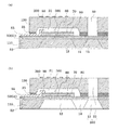
図1は、本実施形態に係るインクジェット式記録ヘッドを示す分解斜視図であり、図2は、図1の平面図及び断面図である。流路形成基板10は、本実施形態では面方位(110)のシリコン単結晶基板からなり、図示するように、この流路形成基板10には、隔壁11によって区画された複数の圧力発生室12がその幅方向に並設されている。また、流路形成基板10の圧力発生室12の長手方向外側の領域には連通部13が形成され、連通部13と各圧力発生室12とが、圧力発生室12毎に設けられたインク供給路14を介して連通されている。連通部13は、後述する保護基板30のリザーバ部32と連通して各圧力発生室12の共通のインク室となるリザーバ100の一部を構成する。インク供給路14は、圧力発生室12よりも狭い幅で形成されており、連通部13から圧力発生室12に流入するインクの流路抵抗を一定に保持している。
Hereinafter, the present invention will be described in detail based on embodiments. In the following embodiments, an ink jet recording head will be described as an example of a liquid jet head manufactured by the manufacturing method according to the present invention.
(Embodiment 1)
FIG. 1 is an exploded perspective view showing an ink jet recording head according to this embodiment, and FIG. 2 is a plan view and a cross-sectional view of FIG. In this embodiment, the flow
なお、流路形成基板10の一方の面には予め熱酸化によって二酸化シリコンからなる厚さ0.5〜2μmの弾性膜50が形成されており、これら圧力発生室12等は、流路形成基板10を弾性膜50に達するまで異方性エッチングすることによって形成されている。
An
流路形成基板10の開口面側には、各圧力発生室12のインク供給路14とは反対側の端部近傍に連通するノズル開口21が穿設されたノズルプレート20が、マスク膜52を介して接着剤や熱溶着フィルム等によって固着されている。なお、ノズルプレート20は、厚さが例えば、0.01〜1mmで、線膨張係数が300℃以下で、例えば2.5〜4.5[×10-6/℃]であるガラスセラミックス、シリコン単結晶基板又はステンレス鋼などからなる。
On the opening surface side of the flow
また、流路形成基板10の表面の弾性膜50上には、厚さが例えば、約0.4μmの絶縁体膜55が形成されている。さらに、この絶縁体膜55上には、厚さが例えば、約0.2μmの下電極膜60と、厚さが例えば、約1.0μmの圧電体層70と、厚さが例えば、約0.05μmの上電極膜80とからなる圧電素子300が形成されている。また、このような各圧電素子300の上電極膜80には、リード電極90がそれぞれ接続され、このリード電極90を介して各圧電素子300に選択的に電圧が印加されるようになっている。
An
さらに、流路形成基板10の圧電素子300側の面には、圧電素子300に対向する領域に圧電素子保持部31を有する保護基板(接合基板)30が接着剤35を介して接合されている。圧電素子300は、この圧電素子保持部31内に形成されているため、外部環境の影響を殆ど受けない状態で保護されている。また、保護基板30には、流路形成基板10の連通部13と連通してリザーバ100を構成するリザーバ部32が形成されている。
Further, a protective substrate (bonding substrate) 30 having a piezoelectric
また、この保護基板30上には、金属膜201を所定形状にパターニングすることによって形成された複数の配線からなる配線パターン200が設けられ、この配線パターン200上には、圧電素子300を駆動するための駆動IC210が実装されている。そして、各圧電素子300から圧電素子保持部31の外側まで引き出された各リード電極90の先端部と、駆動IC210とが駆動配線220を介して電気的に接続されている。
A
なお、配線パターン200を構成する金属膜201の材料としては、例えば、ニッケル(Ni)、クロム(Cr)、チタン(Ti)、タングステン(W)、あるいはこれらの合金等の卑金属材料が挙げられ、本実施形態では、ニッケルクロム(NiCr)を用いている。
Examples of the material of the
また、保護基板30上には、封止膜41及び固定板42とからなるコンプライアンス基板40が接合されてリザーバ部32が封止されている。なお、固定板42のリザーバ部32に対向する領域は、厚さ方向に完全に除去された開口部43となっており、リザーバ部32は、実際には可撓性を有する封止膜41のみで封止されている。
In addition, a
このような本実施形態のインクジェット式記録ヘッドでは、図示しない外部インク供給手段からインクを取り込み、リザーバ100からノズル開口21に至るまで内部をインクで満たした後、駆動IC210からの記録信号に従い、圧力発生室12に対応するそれぞれの下電極膜60と上電極膜80との間に電圧を印加し、圧電素子300及び振動板をたわみ変形させることにより、各圧力発生室12内の圧力が高まりノズル開口21からインクが吐出する。
In such an ink jet recording head of this embodiment, ink is taken in from an external ink supply means (not shown), filled with ink from the
以下、このようなインクジェット式記録ヘッドの製造方法について、図3〜図6を参照して説明する。なお、図3〜図6は、インクジェット式記録ヘッドの製造方法を示す圧力発生室の長手方向の断面図である。 Hereinafter, a method for manufacturing such an ink jet recording head will be described with reference to FIGS. 3 to 6 are cross-sectional views in the longitudinal direction of the pressure generating chamber showing the method of manufacturing the ink jet recording head.
まず、図3(a)に示すように、シリコンウェハである流路形成基板用ウェハ110を約1100℃の拡散炉で熱酸化し、その表面に弾性膜50を構成する二酸化シリコン膜51を形成する。なお、本実施形態では、流路形成基板用ウェハ110として、厚さが約625μmと比較的厚く剛性の高いシリコンウェハを用いている。
First, as shown in FIG. 3A, a channel forming
次に、図3(b)に示すように、弾性膜50(二酸化シリコン膜51)上に、酸化ジルコニウムからなる絶縁体膜55を形成する。具体的には、弾性膜50(二酸化シリコン膜51)上に、例えば、スパッタ法等によりジルコニウム(Zr)層を形成後、このジルコニウム層を、例えば、500〜1200℃の拡散炉で熱酸化することにより酸化ジルコニウム(ZrO2)からなる絶縁体膜55を形成する。
Next, as shown in FIG. 3B, an
次いで、図3(c)に示すように、例えば、白金とイリジウムとを絶縁体膜55上に積層することにより下電極膜60を形成した後、この下電極膜60を所定形状にパターニングする。次に、図3(d)に示すように、例えば、チタン酸ジルコン酸鉛(PZT)等からなる圧電体層70と、例えば、イリジウムからなる上電極膜80とを流路形成基板用ウェハ110の全面に形成し、これら圧電体層70及び上電極膜80を、各圧力発生室12に対向する領域にパターニングして圧電素子300を形成する。次いで、図4(a)に示すように、リード電極90を形成する。具体的には、例えば、金(Au)等からなる配線層95を全面に形成し、この配線層95をパターニングすることにより各圧電素子300から引き出されるリード電極90を形成する。
Next, as shown in FIG. 3C, after the
次に、図4(b)に示すように、保護基板用ウェハ130を、流路形成基板用ウェハ110上に接着剤35によって接着する。ここで、保護基板用ウェハ130の表面には、金属膜201からなる配線パターン200を予め形成しておく。具体的には、まず、図5(a)に示すように、圧電素子保持部31等が形成された保護基板用ウェハ130の表面に、所定の金属材料、本実施形態では、ニッケルクロム(NiCr)からなる金属膜201を形成する。次いで、図5(b)に示すように、金属膜201上に、レジストを塗布・パターニングすることにより、所定形状のレジスト膜230を形成する。次いで、図5(c)に示すように、レジスト膜230で覆われていない領域の金属膜201の表面、すなわち、後のエッチング工程で除去される領域の金属膜201の表面に、金属膜201よりもイオン化傾向の小さい金属粒子240を付着させる。例えば、本実施形態では、金属膜201が形成された保護基板用ウェハ130をめっき浴に数秒〜数分程度浸漬させることによって、金属粒子240を金属膜201の表面に付着させている。
Next, as shown in FIG. 4B, the
この金属粒子240は、金属膜201の表面に点在していればよいが、数nm程度の厚さの実質的な膜として存在していてもよい。すなわち、金属粒子240を付着させる量は特に限定されず、金属膜201の材料等に合わせて適宜決定されればよい。また、金属膜201の表面に付着させる金属粒子240は、金属膜201よりもイオン化傾向の低い金属材料、すなわち、標準単極電位が大きい金属材料であればよいが、金属膜201とのイオン化傾向の差が大きい金属材料の粒子であることが好ましく、例えば、パラジウム(Pd)、金(Au)等の貴金属粒子が挙げられる。
The
このように金属粒子240を金属膜201に付着させた後は、図5(d)に示すように、レジスト膜230を介して金属粒子240が表面に付着した状態の金属膜201をウェットエッチングすることにより、金属膜201を所定形状にパターニングして配線パターン200を形成する。
After the
このように本実施形態では、保護基板用ウェハ130上に配線パターン200を形成する際、金属粒子240を表面に付着させた状態で金属膜201をエッチングするようにした。これにより、金属膜201のエッチングレートは、数倍程度〜数十倍程度まで上昇するため、金属膜201を極めて短時間でパターニングして配線パターン200を形成することができる。したがって、金属膜201のサイドエッチング量が大幅に減少し、また、レジスト膜230がエッチング液によって浸食されてレジスト膜230の下側の金属膜201(配線パターン200)の膜厚が減少してしまうのも防止することができる。すなわち、金属膜201を高精度にパターニングでき、各配線が比較的高密度に配列された配線パターン200を形成することができる。さらに、本実施形態では、レジスト膜230を形成後に、金属膜201の表面に金属粒子240を付着させている。これにより、金属膜201は、除去される部分のみ、エッチングレートが上昇するため、ウェットエッチングによって金属膜201を極めて高精度にパターニングすることができる。
As described above, in the present embodiment, when the
なお、このような効果は、本実施形態のように、金属膜201がイオン化傾向の高い卑金属材料からなる場合に特に効果的である。卑金属材料は、酸化(不動態化)されやすいため、このような卑金属材料からなる金属膜201の表面には酸化膜(不動態膜)が形成されやすい。そしてこのように表面に酸化膜(不動態膜)が形成された金属膜201はエッチングレートが大幅に低下するためエッチングに時間がかかり、その結果、サイドエッチング量が多くなる等の問題が生じてしまう。しかしながら、金属膜201の表面に酸化膜が形成されていても、上述したように、表面に金属粒子240を付着させた状態で金属膜201をウェットエッチングすることにより、極めて短時間でエッチングを終了させることができる。これは、例えば、上述したように金属膜201をめっき浴に浸漬させることで、金属膜201の表面の酸化膜が溶解(ライトエッチング)されて膜厚が薄くなると共に、金属膜201をウェットエッチングする際に、金属膜201と金属粒子240との間で電触が生じることによるものと考えられる。
Such an effect is particularly effective when the
なお、本実施形態では、金属膜201上にレジスト膜230を形成後に、金属粒子240を金属膜201の表面に付着させるようにしたが、これに限定されず、勿論、レジスト膜230を形成する前に、金属粒子240を金属膜201の全面に付着させるようにしてもよい。この場合でも、金属膜201を十分に高精度にパターニングすることができる。
In this embodiment, after the resist
また、レジスト膜230を形成する前に金属粒子240を金属膜201に付着させる場合、例えば、スパッタリング法あるいはCVD法によって金属粒子240を金属膜201の表面に付着させるようにしてもよい。また、例えば、スパッタリング法によって金属粒子240を金属膜201に付着させる場合、スパッタ装置の電極間に実際に電圧を印加しなくても、所定金属の原子又は分子が存在するチャンバ内に、数秒〜数十秒程度、保護基板用ウェハ130(金属膜201)を放置しておけばよい。
Further, when the
ここで、下記実施例1、2及び比較例のパターニング方法で、ニッケルクロム(NiCr)からなる金属膜をパターニングして配線パターンを形成し、そのときのエッチング時間およびサイドエッチング量を調べた結果を下記表1に示す。 Here, with the patterning methods of Examples 1 and 2 and Comparative Example below, a metal film made of nickel chromium (NiCr) was patterned to form a wiring pattern, and the etching time and side etching amount at that time were examined. Shown in Table 1 below.
(実施例1)
厚さが約0.1μmの金属膜が形成された基板を、めっき浴に浸漬させて金属膜の表面に、パラジウム(Pd)である金属粒子を付着させ、その後、約35μm幅のレジスト膜を介して金属膜をウェットエッチングすることによって、配線パターンを形成した。
Example 1
A substrate on which a metal film having a thickness of about 0.1 μm is formed is immersed in a plating bath to deposit metal particles of palladium (Pd) on the surface of the metal film, and then a resist film having a width of about 35 μm is formed. Then, the metal film was wet etched to form a wiring pattern.
(実施例2)
基板上に約0.1μmの厚さで形成された金属膜の表面に、スパッタリング法によって金属粒子を付着させ、その後、実施例1と同様に、金属膜を、約35μm幅のレジスト膜を介してウェットエッチングすることにより配線パターンを形成した。
(Example 2)
Metal particles were deposited on the surface of the metal film formed on the substrate with a thickness of about 0.1 μm by sputtering, and then the metal film was passed through a resist film having a width of about 35 μm as in Example 1. A wiring pattern was formed by wet etching.
(比較例)
基板上に約0.1μmの厚さで形成された金属膜を、表面に金属粒子を付着させることなく、約40μm幅のレジスト膜を介してウェットエッチングして、配線パターンを形成した。
(Comparative example)
A metal film formed with a thickness of about 0.1 μm on the substrate was wet-etched through a resist film with a width of about 40 μm without attaching metal particles to the surface to form a wiring pattern.

上記表1に示すように、実施例1及び2のパターニング方法では、エッチング時間が、比較例のパターニング方法の1/5〜1/6程度まで、大幅に短縮された。また、比較例のパターニング方法では、配線(金属膜)の両サイドでのサイドエッチング量は、それぞれ約12.9μmもあったのに対し、実施例1及び2のパターニング方法では、比較例のパターニング方法の1/3程度まで大幅に減少していた。この結果からも明らかなように、本発明の方法によれば、金属膜を極めて短時間で高精度にパターニングして配線パターンを良好に形成することができる。 As shown in Table 1 above, in the patterning methods of Examples 1 and 2, the etching time was significantly shortened to about 1/5 to 1/6 of the patterning method of the comparative example. In the patterning method of the comparative example, the side etching amount on both sides of the wiring (metal film) was about 12.9 μm, respectively, whereas in the patterning methods of Examples 1 and 2, the patterning of the comparative example was performed. It was greatly reduced to about 1/3 of the method. As is apparent from this result, according to the method of the present invention, the metal film can be patterned with high accuracy in a very short time to form a good wiring pattern.
このような配線パターン200が形成された保護基板用ウェハ130を、流路形成基板用ウェハ110に接合した後は、図4(c)に示すように、流路形成基板用ウェハ110をある程度の厚さとなるまで研磨し、さらにフッ硝酸によってウェットエッチングすることにより所定の厚さに形成する。次いで、図6(a)に示すように、流路形成基板用ウェハ110上に、例えば、窒化シリコン(SiN)からなるマスク膜52を新たに形成して所定形状にパターニングする。そして、図6(b)に示すように、このマスク膜52を介して流路形成基板用ウェハ110を異方性エッチングすることで、圧力発生室12、連通部13及びインク供給路14等を形成する。さらに、弾性膜50及び絶縁体膜55を貫通させて連通部13とリザーバ部32とを連通させてリザーバ100を形成する。
After the
なお、図示しないが、その後、保護基板用ウェハ130に形成されている配線パターン200上に駆動IC210を実装すると共に、駆動IC210とリード電極90とを駆動配線220によって接続する。さらに、流路形成基板用ウェハ110及び保護基板用ウェハ130の外周縁部の不要部分を、例えば、ダイシング等により切断することによって除去する。そして、流路形成基板用ウェハ110の保護基板用ウェハ130とは反対側の面にノズル開口21が穿設されたノズルプレート20を接合すると共に、保護基板用ウェハ130にコンプライアンス基板40を接合し、これら流路形成基板用ウェハ110等を図1に示すような一つのチップサイズの流路形成基板10等に分割することによって上述した構造のインクジェット式記録ヘッドが製造される。
Although not shown, the
(他の実施形態)
以上、本発明の一実施形態を説明したが、本発明は、上述した実施形態に限定されるものではない。例えば、上述した実施形態では、インクジェット式記録ヘッドを例示して本発明を説明したが、本発明は、インク以外の液体を噴射する他の液体噴射ヘッドの製造方法にも勿論適用することができる。なお、その他の液体噴射ヘッドとしては、例えば、プリンタ等の画像記録装置に用いられる各種の記録ヘッド、液晶ディスプレー等のカラーフィルタの製造に用いられる色材噴射ヘッド、有機ELディスプレー、FED(面発光ディスプレー)等の電極形成に用いられる電極材料噴射ヘッド、バイオchip製造に用いられる生体有機物噴射ヘッド等が挙げられる。さらに、本発明のパターニング方法は、あらゆる金属膜のパターニングに適用することができ、勿論、液体噴射ヘッドの製造だけでなく、例えば、半導体デバイス等、あらゆる装置の製造に適用できることは言うまでもない。
(Other embodiments)
Although one embodiment of the present invention has been described above, the present invention is not limited to the above-described embodiment. For example, in the above-described embodiment, the present invention has been described by exemplifying an ink jet recording head. However, the present invention can also be applied to a manufacturing method of another liquid ejecting head that ejects liquid other than ink. . Other liquid ejecting heads include, for example, various recording heads used in image recording apparatuses such as printers, color material ejecting heads used in the manufacture of color filters such as liquid crystal displays, organic EL displays, and FED (surface emitting). Examples thereof include an electrode material ejection head used for electrode formation such as a display, and a bioorganic matter ejection head used for biochip production. Furthermore, the patterning method of the present invention can be applied to patterning of any metal film. Needless to say, the patterning method can be applied not only to the manufacture of a liquid jet head but also to the manufacture of any apparatus such as a semiconductor device.
10 流路形成基板、 20 ノズルプレート、 30 保護基板、 40 コンプライアンス基板、 60 下電極膜、 70 圧電体層、 80 上電極膜、 90 リード電極、 100 リザーバ、 230 レジスト膜、 240 金属粒子、 300 圧電素子
10 flow path forming substrate, 20 nozzle plate, 30 protective substrate, 40 compliance substrate, 60 lower electrode film, 70 piezoelectric layer, 80 upper electrode film, 90 lead electrode, 100 reservoir, 230 resist film, 240 metal particle, 300 piezoelectric element
Claims (8)
請求項1〜6の何れかのパターニング方法を用いて金属材料からなる金属膜をパターニングして、前記圧電素子に接続される配線パターンを形成することを特徴とする液体噴射ヘッドの製造方法。 A liquid ejecting head comprising: a flow path forming substrate provided with a pressure generating chamber communicating with a nozzle opening from which liquid droplets are discharged; and a piezoelectric element provided on one surface side of the flow path forming substrate via a vibration plate A manufacturing method of
A method of manufacturing a liquid jet head, comprising: patterning a metal film made of a metal material using the patterning method according to claim 1 to form a wiring pattern connected to the piezoelectric element.
8. The method of manufacturing a liquid jet head according to claim 7, wherein the wiring pattern is formed on a surface of a bonding substrate bonded to the flow path forming substrate.
Priority Applications (1)
| Application Number | Priority Date | Filing Date | Title |
|---|---|---|---|
| JP2005069552A JP2006248093A (en) | 2005-03-11 | 2005-03-11 | Patterning method and manufacturing method for liquid jet head |
Applications Claiming Priority (1)
| Application Number | Priority Date | Filing Date | Title |
|---|---|---|---|
| JP2005069552A JP2006248093A (en) | 2005-03-11 | 2005-03-11 | Patterning method and manufacturing method for liquid jet head |
Publications (2)
| Publication Number | Publication Date |
|---|---|
| JP2006248093A true JP2006248093A (en) | 2006-09-21 |
| JP2006248093A5 JP2006248093A5 (en) | 2008-04-17 |
Family
ID=37089070
Family Applications (1)
| Application Number | Title | Priority Date | Filing Date |
|---|---|---|---|
| JP2005069552A Withdrawn JP2006248093A (en) | 2005-03-11 | 2005-03-11 | Patterning method and manufacturing method for liquid jet head |
Country Status (1)
| Country | Link |
|---|---|
| JP (1) | JP2006248093A (en) |
Cited By (1)
| Publication number | Priority date | Publication date | Assignee | Title |
|---|---|---|---|---|
| JP2014024214A (en) * | 2012-07-25 | 2014-02-06 | Canon Inc | Method for manufacturing liquid discharge head |
-
2005
- 2005-03-11 JP JP2005069552A patent/JP2006248093A/en not_active Withdrawn
Cited By (2)
| Publication number | Priority date | Publication date | Assignee | Title |
|---|---|---|---|---|
| JP2014024214A (en) * | 2012-07-25 | 2014-02-06 | Canon Inc | Method for manufacturing liquid discharge head |
| US9427953B2 (en) | 2012-07-25 | 2016-08-30 | Canon Kabushiki Kaisha | Method of manufacturing liquid ejection head |
Similar Documents
| Publication | Publication Date | Title |
|---|---|---|
| JP3726909B2 (en) | Method for manufacturing liquid jet head | |
| JP4457649B2 (en) | Liquid ejecting head and liquid ejecting apparatus | |
| JP4645024B2 (en) | Method for manufacturing actuator device | |
| JP4761040B2 (en) | Method for manufacturing silicon device and method for manufacturing liquid jet head | |
| JP2006248093A (en) | Patterning method and manufacturing method for liquid jet head | |
| JP2005119199A (en) | Liquid jetting head and liquid jetting apparatus | |
| JP3551748B2 (en) | Ink jet recording head | |
| JP2003266394A (en) | Method for fabricating silicon device and method of manufacturing ink-jet type recording head and silicon wafer | |
| JP2004284176A (en) | Manufacturing method for liquid injection head | |
| JP4784735B2 (en) | Piezoelectric actuator, liquid ejecting apparatus, and method of manufacturing piezoelectric actuator | |
| JP2005153242A (en) | Manufacturing method for liquid jetting head | |
| US8460948B2 (en) | Method for manufacturing liquid ejecting head | |
| JP3849773B2 (en) | Method for manufacturing liquid jet head | |
| JP2004034555A (en) | Manufacturing method of liquid jet head | |
| JP2006224609A (en) | Method for manufacturing liquid injection head | |
| JP4138293B2 (en) | Silicon device manufacturing method and ink jet recording head manufacturing method | |
| JP2004066537A (en) | Process for manufacturing liquid ejection head | |
| JP5083499B2 (en) | Method for manufacturing actuator device and liquid jet head | |
| JPH1177999A (en) | Ink jet recording head | |
| JP2008200905A (en) | Method for manufacturing liquid jetting head | |
| JP2004042357A (en) | Liquid ejetion head and liquid ejetor | |
| JP2005231263A (en) | Method of manufacturing liquid jet head and liquid jet head | |
| JP2004216707A (en) | Liquid ejection head, its manufacturing process and liquid ejector | |
| JP2007160672A (en) | Board processing method, and manufacturing method for liquid jetting head | |
| JP2008114372A (en) | Manufacturing method for liquid jet head |
Legal Events
| Date | Code | Title | Description |
|---|---|---|---|
| A521 | Written amendment |
Free format text: JAPANESE INTERMEDIATE CODE: A523 Effective date: 20080228 |
|
| A621 | Written request for application examination |
Effective date: 20080228 Free format text: JAPANESE INTERMEDIATE CODE: A621 |
|
| A761 | Written withdrawal of application |
Effective date: 20090120 Free format text: JAPANESE INTERMEDIATE CODE: A761 |