JP2006229665A - Temperature compensation piezo-electric oscillation circuit, and electronic equipment with the circuit arranged therein - Google Patents
Temperature compensation piezo-electric oscillation circuit, and electronic equipment with the circuit arranged therein Download PDFInfo
- Publication number
- JP2006229665A JP2006229665A JP2005041866A JP2005041866A JP2006229665A JP 2006229665 A JP2006229665 A JP 2006229665A JP 2005041866 A JP2005041866 A JP 2005041866A JP 2005041866 A JP2005041866 A JP 2005041866A JP 2006229665 A JP2006229665 A JP 2006229665A
- Authority
- JP
- Japan
- Prior art keywords
- temperature
- circuit
- sensitive
- voltage
- resistor
- Prior art date
- Legal status (The legal status is an assumption and is not a legal conclusion. Google has not performed a legal analysis and makes no representation as to the accuracy of the status listed.)
- Pending
Links
Images
Abstract
Description
本発明は、圧電発振回路、特に周囲の温度に応じて発振周波数が変化しないように圧電発振回路の発振周波数を補正する温度補償圧電発振回路、およびこれを備えた電子装置に関するものである。 The present invention relates to a piezoelectric oscillation circuit, and more particularly to a temperature-compensated piezoelectric oscillation circuit that corrects the oscillation frequency of the piezoelectric oscillation circuit so that the oscillation frequency does not change according to the ambient temperature, and an electronic device including the same.
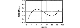
一般に、発振回路は所定周波数で共振する水晶振動子等の圧電共振素子と、該圧電共振素子に接続された増幅回路とを備えている。このような水晶振動子等の圧電共振素子の共振周波数は温度依存性があり、圧電共振素子の温度に応じて共振周波数が変化する。例えば、ATカット水晶振動子(以下、単に「水晶振動子」という。)は低温から高温にかけて周波数が上昇・下降・上昇する周波数温度特性を示す。
この共振周波数が変化する問題を解決する発振回路として、従来から圧電共振素子に接続されたバラクタダイオード等の可変容量素子と、周囲温度に応じて可変容量素子に印加する電圧を変化させる感温抵抗素子回路とを備えた温度補償圧電発振回路が複数提案されている(例えば、特許文献1・特許文献2・特許文献3参照)。
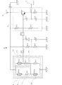
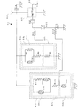
ここで従来の一般的な温度補償圧電発振回路である特許文献1での回路構成例を図1に示す。図1に示すように温度補償圧電発振回路1は、圧電共振素子である水晶振動子XD1と、水晶振動子XD1の一方端に接続する増幅回路4と、水晶振動子XD1の他方端に接続する可変容量素子(バラクタダイオードVD1)とを備える。
In general, an oscillation circuit includes a piezoelectric resonance element such as a crystal resonator that resonates at a predetermined frequency, and an amplification circuit connected to the piezoelectric resonance element. The resonance frequency of such a piezoelectric resonator such as a crystal resonator has temperature dependence, and the resonance frequency changes according to the temperature of the piezoelectric resonator. For example, an AT-cut crystal resonator (hereinafter simply referred to as “crystal resonator”) exhibits frequency-temperature characteristics in which the frequency increases, decreases, and increases from a low temperature to a high temperature.
As an oscillation circuit that solves the problem of changing the resonance frequency, a variable capacitance element such as a varactor diode that has been conventionally connected to a piezoelectric resonance element and a temperature-sensitive resistor that changes the voltage applied to the variable capacitance element according to the ambient temperature A plurality of temperature compensated piezoelectric oscillation circuits including element circuits have been proposed (see, for example,
Here, FIG. 1 shows a circuit configuration example in
このバラクタダイオードVD1のカソードには抵抗器R6を介して感温抵抗素子回路5が接続される。また、バラクタダイオードVD1のアノードには、バイアス回路である抵抗器R4・抵抗器R5による分圧回路の分圧点が接続され、分圧点にさらに直流電流遮断用のコンデンサC5が接続される。
A temperature sensitive
感温抵抗素子回路5は、感温抵抗素子であるサーミスタTH1・サーミスタTH2・サーミスタTH3と抵抗器R7・抵抗器R8・抵抗器R9を備える。サーミスタTH2・サーミスタTH3・抵抗器R8・抵抗器R9からなる回路は分圧回路6aとして作用し、サーミスタTH1・抵抗器R7からなる回路は分圧回路6bとして作用する。このため、この感温抵抗素子回路5では、分圧回路6aと分圧回路6bとによって、電源電圧に対して2段階の分圧が行われる。
The temperature sensitive
分圧回路6aでは、第1抵抗回路7aとしてサーミスタTH2・抵抗器R8を直列に接続し、サーミスタTH2の一方端を電源電圧Vcc端子2に接続している。また第2抵抗回路8aとしてサーミスタTH3・抵抗器R9を並列に接続し、一方端を接地している。そして第1抵抗回路7aと第2抵抗回路8aを直列接続し、接続点を分圧回路6bに接続している。
In the voltage dividing circuit 6a, the thermistor TH2 and the resistor R8 are connected in series as the first resistor circuit 7a, and one end of the thermistor TH2 is connected to the power supply
分圧回路6bでは、第1抵抗回路7bであるサーミスタTH1の一方端を電源電圧Vcc端子2に接続している。また第2抵抗回路8bである抵抗器R7の一方端を分圧回路6aの分圧点に接続している。そして、第1抵抗回路7bであるサーミスタTH1と第2抵抗回路8bである抵抗器R7を直列接続し、接続点をバラクタダイオードVD1のカソードに抵抗器R6を介して接続している。
In the voltage dividing circuit 6b, one end of the thermistor TH1, which is the first resistance circuit 7b, is connected to the power supply
このような構成のもと圧電共振素子として共振周波数が変化する水晶振動子XD1を用いた温度補償圧電発振回路1では、水晶振動子XD1と、可変容量素子であるバラクタダイオードVD1との合成キャパシタンスに回路の共振周波数が依存する。そのため、バラクタダイオードVD1に印加する電圧を調整すれば、バラクタダイオードVD1のキャパシタンスが変化し、この結果、水晶振動子XD1との合成キャパシタンスが変化して、共振周波数が変化する。この変化量を水晶振動子XD1の温度による共振周波数の変化を打ち消すように設定しておけば、周囲温度による影響の少ない略一定の共振周波数の高周波信号を得ることができる。
In the temperature compensated
そこで感温抵抗素子回路5の出力電圧をバラクタダイオードVD1のカソード端子に印加して合成キャパシタンスを設定し、水晶振動子XD1との合成キャパシタンスによる共振周波数の変化と、温度変化によるバラクタダイオードVD1の発振周波数の変化とを相殺させて発振器の温度補償を行っている。
Therefore, the output voltage of the temperature-sensitive
すなわち上述のように水晶振動子XD1は低温から高温にかけて周波数が上昇・下降・上昇する温度特性を示すため、バラクタダイオードDV1への印加電圧が低温から高温にかけて下降・上昇・下降するように感温抵抗素子回路5の感温抵抗素子の抵抗温度特性を設定する。
That is, as described above, the crystal resonator XD1 exhibits temperature characteristics in which the frequency rises, falls, and rises from low temperature to high temperature. Therefore, the temperature sensitivity is such that the voltage applied to the varactor diode DV1 falls, rises, and falls from low temperature to high temperature. The resistance temperature characteristic of the temperature sensitive resistance element of the
そこで、上述の感温抵抗素子回路5の構成では、電圧が下降してから上昇する低温の温度域、電圧が下降してから上昇する高温の温度域、全体の温度域、のそれぞれの調整用に感温抵抗素子回路5にサーミスタを3つ設けて比較的に高精度な調整を可能とする。例えばサーミスタTH2と抵抗器R8を低温の温度域に対応させ、サーミスタTH1と抵抗器R7を高温の温度域に対応させ、サーミスタTH3と抵抗器R9を全体の温度域に対応させ調整する。このように調整することで従来は主として作用する温度域をサーミスタに対応付け、それぞれを調整することで適切な温度補償電圧が形成されるように3つのサーミスタで感温抵抗素子回路を形成していた。
Therefore, in the above-described configuration of the temperature-sensitive
このように温度補償圧電発振回路1の発振周波数の精度を向上させるためにはサーミスタの個数が複数個必要であるが、温度補償電圧の調整をさらに容易にし、より精緻に設定することができる温度補償圧電発振回路が特許文献2で示されている。この特許文献2では感温抵抗素子回路においてさらにサーミスタの個数を増やすために、分圧回路による分圧を複数回繰り返すことで、温度補償電圧の設定をより詳細に行う。
As described above, in order to improve the accuracy of the oscillation frequency of the temperature compensated
また、より広い温度範囲で温度補償電圧の調整を可能にするため、サーミスタを感温抵抗素子回路に適用した温度補償圧電発振回路をバラクタダイオードの両端に接続し、それぞれの感温抵抗素子の動作を温度によってスイッチする構成が特許文献3で示されている。
上述の特許文献2のようにサーミスタの個数を増やすために感温抵抗素子回路を複数段の分圧回路で構成した場合、サーミスタが増えることにより温度補償電圧の調整を精緻に行うことができるようになる。しかし、単純にサーミスタ数を増やすのみでは、充分な温度補償の精度を得ることはできない。
When the temperature sensitive resistance element circuit is constituted by a plurality of voltage dividing circuits in order to increase the number of thermistors as in the above-mentioned
すなわち感温抵抗素子回路を複数段に接続した分圧回路で構成すると、この感温抵抗素子回路では複数段に形成された分圧回路のうち、前段の分圧回路のダイナミックレンジよりも後段の分圧回路のダイナミックレンジが小さくなる。すなわち、感温抵抗素子回路としての出力電圧のダイナミックレンジが小さなものとなり、実装に際して必要なダイナミックレンジを得られない。そのため、従来の温度補償圧電発振回路では、特許文献2のように必要な大きさのダイナミックレンジを得るために感温抵抗素子回路に増幅器を併設する必要があり、回路構成が複雑化し部品点数が増加していた。
That is, when the temperature-sensitive resistor element circuit is constituted by a voltage dividing circuit connected in a plurality of stages, in this temperature-sensitive resistor element circuit, among the voltage dividing circuits formed in a plurality of stages, the latter stage of the dynamic range of the voltage dividing circuit in the preceding stage is used. The dynamic range of the voltage divider circuit is reduced. That is, the dynamic range of the output voltage as the temperature-sensitive resistance element circuit becomes small, and the dynamic range necessary for mounting cannot be obtained. Therefore, in the conventional temperature-compensated piezoelectric oscillation circuit, it is necessary to add an amplifier to the temperature-sensitive resistance element circuit in order to obtain a dynamic range of a required size as in
また、このような構成の感温抵抗素子回路では、後段の分圧回路における抵抗回路のインピーダンスを、前段の分圧回路における抵抗回路のインピーダンスよりも常に十分に大きくなるようにする必要があり、分圧の段数が多くなると、より後段の分圧回路における抵抗回路のインピーダンスは非常に大きなものになる。しかしながら、選択できるサーミスタの種類には限度があるために、実装に際して選定可能なサーミスタのB定数および抵抗値が制限されてしまい、また実装可能なサーミスタの数の制限が生じる。 Further, in the temperature-sensitive resistance element circuit having such a configuration, it is necessary that the impedance of the resistance circuit in the subsequent voltage dividing circuit is always sufficiently larger than the impedance of the resistance circuit in the previous voltage dividing circuit. When the number of voltage dividing stages increases, the impedance of the resistance circuit in the subsequent voltage dividing circuit becomes very large. However, since there are limits on the types of thermistors that can be selected, the B constant and resistance value of the selectable thermistors are limited during mounting, and the number of thermistors that can be mounted is limited.
また、サーミスタの個数を従来以上に増やすために複数段の分圧回路で感温抵抗素子回路を構成すると、抵抗の小さいサーミスタを用いる必要が生じ、そのサーミスタに流れる電流による自己発熱を無視できない場合があった。すると、そのサーミスタの温度補償電圧の設定精度の向上は困難になり、また消費電力の増加なども生じる。 Also, if a temperature-sensitive resistor element circuit is configured with a multi-stage voltage divider circuit to increase the number of thermistors more than before, it is necessary to use a thermistor with a low resistance, and self-heating due to the current flowing through the thermistor cannot be ignored. was there. Then, it becomes difficult to improve the setting accuracy of the temperature compensation voltage of the thermistor, and the power consumption increases.
さらに、特許文献3のように温度補償圧電発振回路を構成した場合には、温度域ごとに動作する感温抵抗素子回路を切り換えるスイッチ素子が必要であり、また使用時に動作しているサーミスタは、一部のみであり、感温抵抗素子回路の出力である温度補償電圧の精度向上には寄与するものではなかった。
Furthermore, when a temperature compensated piezoelectric oscillation circuit is configured as in
以上のように従来の技術ではより精緻に温度補償電圧を設定するにはより複雑な回路が必要であり、高精度な設定を図ることに困難があった。 As described above, in the conventional technique, a more complicated circuit is required to set the temperature compensation voltage more precisely, and it has been difficult to set with high accuracy.
そこで本発明は、上述のさまざまな問題を解決して、簡易な構成で高精度に温度補償電圧の設定を図ることができる温度補償圧電発振回路およびそれを備えた電子装置を提供することを目的とする。 Accordingly, an object of the present invention is to provide a temperature compensated piezoelectric oscillation circuit that can solve the above-described various problems and can set the temperature compensated voltage with high accuracy with a simple configuration, and an electronic device including the temperature compensated piezoelectric oscillator circuit. And
ここで分圧回路という回路を定義付ける。この分圧回路とは、第1抵抗回路と第2抵抗回路とを直列に接続し、第1抵抗回路と第2抵抗回路との接続点から分圧電圧を引き出し、第1抵抗回路と第2抵抗回路との、少なくとも一方に感温抵抗素子を備える回路とする。また、感温抵抗素子回路という回路を定義づける。この感温抵抗素子回路とは、すくなくとも1つ以上の分圧回路を備え、可変容量素子の1つの端子に常に出力電圧を印加するよう接続された回路のこととする。 Here, a circuit called a voltage dividing circuit is defined. In this voltage dividing circuit, a first resistor circuit and a second resistor circuit are connected in series, a divided voltage is drawn from a connection point between the first resistor circuit and the second resistor circuit, and the first resistor circuit and the second resistor circuit are connected. A circuit including a temperature-sensitive resistance element in at least one of the resistance circuit is used. In addition, a circuit called a temperature sensitive resistance element circuit is defined. The temperature-sensitive resistance element circuit is a circuit that includes at least one voltage dividing circuit and is connected to always apply an output voltage to one terminal of the variable capacitance element.
なお、分圧回路の出力をそのまま感温抵抗素子回路の出力とするのはもちろんだが、分圧回路の出力を、サーミスタを含まない単なる抵抗のみの回路で更に分圧して出力するような構成についても、本発明は除外するものではない。但し、この場合の単なる抵抗のみの回路は本発明の定義による分圧回路には含めない。 Of course, the output of the voltage divider circuit is used as the output of the temperature-sensitive resistor element circuit as it is, but the output of the voltage divider circuit is further divided by a simple resistor-only circuit that does not include the thermistor. However, the present invention is not excluded. In this case, however, a circuit having only a resistor is not included in the voltage dividing circuit according to the definition of the present invention.
本発明は上述の定義のもと、複数の感温抵抗素子回路の出力電圧を可変容量素子に常に印加する。そして、全ての感温抵抗素子回路に含まれる感温抵抗素子の合計数が4つ以上となるように、それぞれの感温抵抗素子回路を構成する。 In the present invention, the output voltages of the plurality of temperature sensitive resistance element circuits are always applied to the variable capacitance element based on the above definition. And each temperature-sensitive resistance element circuit is comprised so that the total number of the temperature-sensitive resistance elements contained in all the temperature-sensitive resistance element circuits may be four or more.
この構成により本発明の温度補償圧電発振回路では、サーミスタを複数の感温抵抗素子回路に分けて設ける。すると、特別な回路、例えば増幅器やスイッチ回路を設けずに、簡易な回路で従来より多くの感温抵抗素子を設けることができる。それぞれの感温抵抗素子回路においては、含まれる感温抵抗素子の設定を、他の感温抵抗素子回路によらずに定めることができ、従来の全てのサーミスタを1つの感温抵抗素子回路に設けていた温度補償圧電発振回路に比べ、多くのサーミスタを設けることができる。さらに感温抵抗素子の数を、従来の3つよりも多い4つ以上とするため、温度補償電圧を高精度に設定できる。また通常は温度補償できなかった温度域でも、設定によって優れた精度で共振周波数を補償することができる。 With this configuration, in the temperature compensated piezoelectric oscillation circuit of the present invention, the thermistor is divided into a plurality of temperature sensitive resistance element circuits. Then, more temperature-sensitive resistance elements can be provided with a simple circuit without providing a special circuit such as an amplifier or a switch circuit. In each temperature-sensitive resistor element circuit, the setting of the temperature-sensitive resistor element included can be determined without depending on other temperature-sensitive resistor element circuits, and all the conventional thermistors are integrated into one temperature-sensitive resistor element circuit. Many thermistors can be provided as compared with the temperature compensated piezoelectric oscillation circuit provided. Furthermore, since the number of temperature sensitive resistance elements is four or more, which is larger than the conventional three, the temperature compensation voltage can be set with high accuracy. Further, the resonance frequency can be compensated with excellent accuracy by setting even in a temperature range in which temperature compensation could not normally be performed.
また本発明は上述の定義のもと、少なくとも1つの感温抵抗素子回路に複数の前記分圧回路を備える。そしてその感温抵抗素子回路では、いずれかの分圧回路の分圧電圧を別の分圧回路でさらに分圧するように接続する。 According to the present invention, a plurality of the voltage dividing circuits are provided in at least one temperature-sensitive resistance element circuit based on the above definition. In the temperature-sensitive resistance element circuit, the divided voltage of one of the voltage dividing circuits is connected so as to be further divided by another voltage dividing circuit.
このような構成により、本発明の温度補償圧電発振回路は、複数段に接続した分圧回路で感温抵抗素子回路を構成する。このように複数段で分圧回路を接続した構成では、温度補償電圧が容易に設定できる。また、従来の複数段で分圧回路を接続した構成とくらべ分圧の段数を同じまたは減らしながら、感温抵抗素子の個数を増やすことができる。 With such a configuration, the temperature-compensated piezoelectric oscillation circuit of the present invention forms a temperature-sensitive resistor element circuit with voltage dividing circuits connected in a plurality of stages. In such a configuration in which the voltage dividing circuits are connected in a plurality of stages, the temperature compensation voltage can be easily set. In addition, the number of temperature-sensitive resistance elements can be increased while the number of voltage dividing stages is the same as or reduced compared to a conventional configuration in which voltage dividing circuits are connected in a plurality of stages.
従来の場合、分圧の段数が多いため後段の分圧回路からの出力電圧のダイナミックレンジが減少していた。しかし本発明によって分圧の段数を抑制すると、実装に充分な大きさのダイナミックレンジを得ることができる。すくなくとも一つの感温抵抗素子回路で充分な大きさのダイナミックレンジを発生させると、他の感温抵抗素子回路のダイナミックレンジが小さくとも温度補償圧電発信回路として必要なダイナミックレンジを確保することができる。また従来は非常に小さな抵抗値の感温抵抗素子を用いる必要があり、すると回路に流れる電流による感温抵抗素子の自己発熱が増加するという問題があった。しかし本発明によれば小さな抵抗値の感温抵抗素子を用いることが不用になり、その結果、自己発熱の問題を解消できる。また従来は後段の分圧回路における抵抗回路のインピーダンスを大きくする必要があった。しかし本発明によれば、限られた感温抵抗素子の種類の中で実装に必要なB定数および抵抗値を選択しても、後段の分圧回路における抵抗回路のインピーダンスの大きさを抑制することができる。 In the conventional case, since the number of voltage dividing stages is large, the dynamic range of the output voltage from the subsequent voltage dividing circuit is reduced. However, if the number of partial pressure stages is suppressed according to the present invention, a dynamic range large enough for mounting can be obtained. When a sufficiently large dynamic range is generated with at least one temperature-sensitive resistor element circuit, the dynamic range required for a temperature-compensated piezoelectric transmission circuit can be secured even if the other temperature-sensitive resistor element circuits have a small dynamic range. . Conventionally, it is necessary to use a temperature-sensitive resistance element having a very small resistance value, and there is a problem that self-heating of the temperature-sensitive resistance element due to a current flowing in the circuit increases. However, according to the present invention, it becomes unnecessary to use a temperature-sensitive resistance element having a small resistance value, and as a result, the problem of self-heating can be solved. Conventionally, it has been necessary to increase the impedance of the resistance circuit in the subsequent voltage dividing circuit. However, according to the present invention, even if the B constant and the resistance value necessary for mounting are selected from the limited types of temperature-sensitive resistance elements, the magnitude of the impedance of the resistance circuit in the subsequent voltage dividing circuit is suppressed. be able to.
また本発明は上述の定義のもと、分圧回路の分圧電圧を別の分圧回路でさらに分圧するように接続した感温抵抗素子回路の、分圧回路の数を最大でも2つとする。 Further, according to the present invention, the number of voltage dividing circuits of the temperature-sensitive resistance element circuit connected so as to further divide the divided voltage of the voltage dividing circuit by another voltage dividing circuit is two at the maximum. .
この構成により本発明の温度補償圧電発振回路では、従来よりサーミスタの選定に制限が無くなり、抵抗温度特性であるB定数や無負荷時抵抗値の調整を容易にできる。また簡易な回路構造を実現できる。 With this configuration, in the temperature compensated piezoelectric oscillation circuit of the present invention, selection of the thermistor is no longer limited, and the B constant, which is a resistance temperature characteristic, and the resistance value at no load can be easily adjusted. In addition, a simple circuit structure can be realized.
また本発明は上述の定義のもと、いずれかの感温抵抗素子回路を、感温抵抗素子を1つ含む分圧回路と、感温抵抗素子を2つ含む分圧回路とで構成する。 Further, according to the present invention, any one of the temperature sensitive resistance element circuits is constituted by a voltage dividing circuit including one temperature sensitive resistance element and a voltage dividing circuit including two temperature sensitive resistance elements.
この構成によりこの感温抵抗素子回路に含まれる感温抵抗素子の数は3つとなるとともに、その3つの感温抵抗素子の調整により、温度補償電圧の全体の曲率や傾き調整用の感温抵抗素子と、低温の温度域での曲率や傾き調整用の感温抵抗素子と、高温の温度域での曲率や傾き調整用の感温抵抗素子とを分けて行うことができるようになる。通常は2つの感温抵抗素子が含まれるほうの分圧回路を高温と低温の調整用とし、1つの感温抵抗素子が含まれるほうの分圧回路を全体の温度域の調整用とするとさらに設定が容易である。 With this configuration, the number of temperature sensitive resistance elements included in the temperature sensitive resistance element circuit is three, and by adjusting the three temperature sensitive resistance elements, the temperature compensation resistance for adjusting the overall curvature and inclination of the temperature compensation voltage is adjusted. It is possible to separately perform an element, a temperature-sensitive resistance element for adjusting curvature and inclination in a low temperature range, and a temperature-sensitive resistance element for adjusting curvature and inclination in a high temperature range. Usually, the voltage divider circuit that includes two temperature-sensitive resistance elements is used for adjustment of high temperature and low temperature, and the voltage divider circuit that includes one temperature-sensitive resistance element is used for adjustment of the entire temperature range. Easy to set up.
また本発明は上述の定義のもと、複数の可変容量素子を備え、複数の感温抵抗素子回路をそれぞれ異なる可変容量素子の端子に接続する。 Further, the present invention includes a plurality of variable capacitance elements based on the above definition, and connects the plurality of temperature sensitive resistance element circuits to terminals of different variable capacitance elements.
この構成により本発明の温度補償圧電発振回路は、可変容量素子の数が増える。すると1つの可変容量素子は複数の端子を備えるため、より多くの感温抵抗素子回路を設けることができる。これにより、簡易な回路でさらに多くの感温抵抗素子を設けるとともに、それぞれの感温抵抗素子回路に含まれる感温抵抗素子の設定を、他の感温抵抗素子回路によらずに定めることができ、サーミスタの選定上の制限が減少する。また、例えば可変容量素子の1つの端子にのみ感温抵抗素子回路を設けた場合には、その可変容量素子のキャパシタンスの設定が容易になる。 This configuration increases the number of variable capacitance elements in the temperature compensated piezoelectric oscillation circuit of the present invention. Then, since one variable capacitance element includes a plurality of terminals, more temperature-sensitive resistance element circuits can be provided. As a result, more temperature sensitive resistance elements can be provided with a simple circuit, and the setting of the temperature sensitive resistance elements included in each temperature sensitive resistance element circuit can be determined without depending on other temperature sensitive resistance element circuits. This reduces the restrictions on thermistor selection. For example, when a temperature-sensitive resistor element circuit is provided only at one terminal of a variable capacitance element, the capacitance of the variable capacitance element can be easily set.
また本発明は上述の定義のもと、可変容量素子の両端の端子に、それぞれ感温抵抗素子回路を接続する。 Further, according to the present invention, a temperature sensitive resistance element circuit is connected to terminals at both ends of the variable capacitance element based on the above definition.
このような構成により、この可変容量素子に印加する電圧をより精緻に設定することができる。この可変容量素子のキャパシタンスを2つの感温抵抗素子回路からの出力電圧で形成するため、可変容量素子にかかる印加電圧のダイナミックレンジを大きく設定することができる。 With such a configuration, the voltage applied to the variable capacitance element can be set more precisely. Since the capacitance of the variable capacitance element is formed by the output voltages from the two temperature-sensitive resistance element circuits, the dynamic range of the applied voltage applied to the variable capacitance element can be set large.
また本発明は上述の定義のもと、全ての前記感温抵抗素子回路のうち、2つの感温抵抗素子回路の接続構造を略同一のものとし、それぞれの感温抵抗素子回路は電源側と接地側との位置を入れ替えて上下反転させて用いる。 Further, the present invention is based on the above definition, and the connection structure of two temperature-sensitive resistor elements among all the temperature-sensitive resistor element circuits is substantially the same, and each temperature-sensitive resistor element circuit is connected to the power supply side. The position is changed upside down by changing the position with the ground side.
このような構成により、2つの感温抵抗素子回路が、ほぼ同一の接続構造で電源側の端子と接地側の端子を入れ替えて上下反転させたような回路構成となる。そのため、これらの感温抵抗素子回路の回路構成を簡易なものとすることができるとともに、容易に温度補償電圧の設定が行える。 With such a configuration, the two temperature-sensitive resistance element circuits have a circuit configuration in which the power supply side terminal and the ground side terminal are switched upside down with substantially the same connection structure. Therefore, the circuit configuration of these temperature-sensitive resistance element circuits can be simplified, and the temperature compensation voltage can be easily set.
また本発明は上述の定義のもと、最も感温抵抗素子の数が多い感温抵抗素子回路では、使用温度域での抵抗温度特性が異なる複数の感温抵抗素子を、分圧回路ごとに異ならせて配置し、最多段数の感温抵抗素子回路に用いた複数の感温抵抗素子のうちいずれかの感温抵抗素子と略同一の抵抗温度特性の感温抵抗素子のみで他の感温抵抗素子回路を構成する。 Further, according to the present invention, based on the above-described definition, in a temperature-sensitive resistance element circuit having the largest number of temperature-sensitive resistance elements, a plurality of temperature-sensitive resistance elements having different resistance temperature characteristics in the operating temperature range are provided for each voltage dividing circuit. The other temperature sensing elements are arranged in a different manner, and only one temperature sensing resistance element having substantially the same resistance temperature characteristics as any one of the plurality of temperature sensing resistance elements used in the temperature sensing resistance element circuit having the largest number of stages. A resistive element circuit is configured.
このような構成により、異なる感温抵抗素子回路との間で、用いる感温抵抗素子の種類を共通化できるため、従来よりも感温抵抗素子回路を簡易化できる。 With such a configuration, the type of the temperature sensitive resistance element to be used can be shared among different temperature sensitive resistance element circuits, and therefore the temperature sensitive resistance element circuit can be simplified as compared with the conventional one.
また本発明は上述の定義のもと、3つの感温抵抗素子回路の出力電圧を複数の可変容量素子に常に印加する。そして、全ての感温抵抗素子回路に含まれる感温抵抗素子の合計数が3つとなるように、それぞれの感温抵抗素子回路を構成する。 Further, according to the present invention, the output voltages of the three temperature-sensitive resistance element circuits are always applied to a plurality of variable capacitance elements based on the above definition. And each temperature-sensitive resistance element circuit is comprised so that the total number of the temperature-sensitive resistance elements contained in all the temperature-sensitive resistance element circuits may be set to three.
この構成により本発明の温度補償圧電発振回路では、サーミスタを複数の感温抵抗素子回路に分けて設ける。すると感温抵抗素子の数が従来と同様に3つであっても、それぞれの感温抵抗素子回路においては、含まれる感温抵抗素子の設定を、他の感温抵抗素子回路によらずに定めることができる。 With this configuration, in the temperature compensated piezoelectric oscillation circuit of the present invention, the thermistor is divided into a plurality of temperature sensitive resistance element circuits. Then, even if the number of the temperature sensitive resistance elements is three as in the conventional case, in each temperature sensitive resistance element circuit, the setting of the temperature sensitive resistance elements included is not performed by other temperature sensitive resistance element circuits. Can be determined.
また本発明は上述の定義のもと、1つの感温抵抗素子回路に2つの前記分圧回路を備える。そしてその感温抵抗素子回路では、一方の分圧回路の分圧電圧を他方の分圧回路でさらに分圧するように接続する。そして、全ての感温抵抗素子回路に含まれる感温抵抗素子の合計数が3つとなるように、それぞれの感温抵抗素子回路を構成する。 Further, according to the present invention, the two voltage dividing circuits are provided in one temperature-sensitive resistance element circuit based on the above definition. In the temperature-sensitive resistance element circuit, the divided voltage of one voltage dividing circuit is connected so as to be further divided by the other voltage dividing circuit. And each temperature-sensitive resistance element circuit is comprised so that the total number of the temperature-sensitive resistance elements contained in all the temperature-sensitive resistance element circuits may be set to three.
この構成により本発明の温度補償圧電発振回路では、サーミスタを複数の感温抵抗素子回路に分けて設ける。すると感温抵抗素子の数が従来と同様に3つであっても、それぞれの感温抵抗素子回路においては、含まれる感温抵抗素子の設定を、他の感温抵抗素子回路によらずに定めることができる。このように複数段で分圧回路を接続した構成では、従来よりサーミスタの選定に制限が無くなり、抵抗温度特性であるB定数や無負荷時抵抗値の調整を容易にできる。また簡易な回路構造を実現できる。 With this configuration, in the temperature compensated piezoelectric oscillation circuit of the present invention, the thermistor is divided into a plurality of temperature sensitive resistance element circuits. Then, even if the number of the temperature sensitive resistance elements is three as in the conventional case, in each temperature sensitive resistance element circuit, the setting of the temperature sensitive resistance elements included is not performed by other temperature sensitive resistance element circuits. Can be determined. In the configuration in which the voltage dividing circuits are connected in a plurality of stages as described above, the selection of the thermistor is not limited as in the prior art, and the B constant, which is a resistance temperature characteristic, and the resistance value at no load can be easily adjusted. In addition, a simple circuit structure can be realized.
また本発明は上述の定義のもと、上述の構成の温度補償圧電発振回路を備えて電子装置を構成する。 According to the present invention, an electronic device is configured with the temperature compensated piezoelectric oscillation circuit having the above-described configuration based on the above-described definition.
このような構成により、より高精度に温度補償のされた電子装置を得ることができる。 With such a configuration, it is possible to obtain an electronic device that is temperature-compensated with higher accuracy.
本発明によれば、従来の問題を解決し、簡易な回路で温度に対する周波数の安定性に優れた発振回路を形成するとともに高精度な温度補償を行う電子装置を実現できる。 According to the present invention, it is possible to realize an electronic device that solves the conventional problems and forms an oscillation circuit that is excellent in frequency stability with respect to temperature with a simple circuit and performs highly accurate temperature compensation.
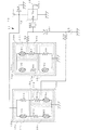
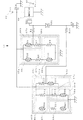
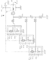
以下に、第1の実施形態を示す。図2は第1の実施形態に係る温度補償圧電発振回路11を含み、コルピッツ発振回路の負性抵抗発生部分を増幅回路14として設けた回路図の例である。
The first embodiment is shown below. FIG. 2 is an example of a circuit diagram that includes the temperature-compensated
増幅回路14としては、ここでは上述の従来例の図1で示した増幅回路4と同一なコルピッツ発振回路の負性抵抗発生部分を設けている。そのため、図1の増幅回路4をもとにこの増幅回路14を説明する。
As the amplifying
増幅回路14では、水晶振動子XD1をトランジスタQ1のベースに接続している。また、トランジスタQ1のコレクタを電源電圧Vcc端子12に接続し、エミッタを抵抗器R1およびコンデンサC2を介して接地している。また、トランジスタQ1のエミッタとベースとの間には、帰還用コンデンサC1を接続し、ベースにはさらに抵抗器R3・抵抗器R2によるベースバイアス回路を接続している。また、トランジスタQ1のエミッタは、コンデンサC3を介して信号出力Vout端子13に接続している。また、トランジスタQ1のコレクタはコンデンサC4を介して高周波的に接地している。この結果、トランジスタQ1は水晶振動子XD1の共振周波数で負性抵抗回路として作用する。
In the
また、図2に示すように温度補償圧電発振回路11は、圧電共振素子である水晶振動子XD1と、水晶振動子XD1の一方端に接続する増幅回路14と、水晶振動子XD1の他方端に接続する可変容量素子(バラクタダイオードVD1)を備える。バラクタダイオードVD1のアノードは水晶振動子XD1と接続し、このバラクタダイオードVD1のアノードにはさらに抵抗器R6を介して感温抵抗素子回路15aを接続している。また、バラクタダイオードVD1のカソードには抵抗器R10を介して感温抵抗素子回路15bを接続し、さらに直流電流遮断用のコンデンサC5を介して接地している。
Further, as shown in FIG. 2, the temperature compensated
感温抵抗素子回路15aは、感温抵抗素子である負特性のサーミスタTH1・サーミスタTH2・サーミスタTH3と、抵抗器R7・抵抗器R8・抵抗器R9とを備えている。これらの素子のうち、サーミスタTH2・サーミスタTH3・抵抗器R8・抵抗器R9からなる回路は分圧回路16aとして作用する。また、サーミスタTH1・抵抗器R7からなる回路は分圧回路16bとして作用する。そのため、この感温抵抗素子回路15aは、分圧回路16aと分圧回路16bによる2段の分圧を行う。 The temperature-sensitive resistance element circuit 15a includes a thermistor TH1, thermistor TH2, and thermistor TH3, which are temperature-sensitive resistance elements, and a resistor R7, a resistor R8, and a resistor R9. Among these elements, a circuit comprising the thermistor TH2, the thermistor TH3, the resistor R8, and the resistor R9 functions as a voltage dividing circuit 16a. Further, a circuit composed of the thermistor TH1 and the resistor R7 functions as a voltage dividing circuit 16b. Therefore, this temperature-sensitive resistance element circuit 15a performs two-stage voltage division by the voltage dividing circuit 16a and the voltage dividing circuit 16b.
分圧回路16aでは第1抵抗回路17aとして、サーミスタTH2・抵抗器R8を直列接続し、サーミスタTH2の一方端を電源電圧Vcc端子12に接続している。また、第2抵抗回路18aとして、サーミスタTH3・抵抗器R9を並列に接続し、一方端を接地している。そして、第1抵抗回路17aと第2抵抗回路18aを直列接続し、接続点を分圧回路16bに接続している。
In the voltage dividing circuit 16a, as the first resistor circuit 17a, the thermistor TH2 and the resistor R8 are connected in series, and one end of the thermistor TH2 is connected to the power supply
分圧回路16bでは、第1抵抗回路17bであるサーミスタTH1の一方端を電源電圧Vcc端子12に接続している。また、第2抵抗回路18bである抵抗器R7の一方端を分圧回路16aの分圧点に接続している。そして、第1抵抗回路17bであるサーミスタTH1と第2抵抗回路18bである抵抗器R7を直列接続し、接続点をバラクタダイオードVD1のアノードに抵抗器R6を介して接続している。
In the voltage dividing circuit 16b, one end of the thermistor TH1, which is the first resistance circuit 17b, is connected to the power supply
また、感温抵抗素子回路15bは、負特性のサーミスタTH4・サーミスタTH5・サーミスタTH6と抵抗器R11・抵抗器R12・抵抗器R13を備えている。サーミスタTH5・サーミスタTH6・抵抗器R12・抵抗器R13からなる回路は分圧回路16cとして作用し、また、サーミスタTH4・抵抗器R11からなる回路は分圧回路16dとして作用する。そのため、この感温抵抗素子回路15bは、分圧回路16cと分圧回路16dによる2段の分圧を行う。 The temperature-sensitive resistor element circuit 15b includes a thermistor TH4, thermistor TH5, thermistor TH6, a resistor R11, a resistor R12, and a resistor R13 having negative characteristics. A circuit comprising the thermistor TH5, the thermistor TH6, the resistor R12, and the resistor R13 acts as a voltage dividing circuit 16c, and a circuit comprising the thermistor TH4 and the resistor R11 acts as a voltage dividing circuit 16d. Therefore, this temperature-sensitive resistance element circuit 15b performs two-stage voltage division by the voltage dividing circuit 16c and the voltage dividing circuit 16d.
分圧回路16cでは、第1抵抗回路17cとしてサーミスタTH6・抵抗器R13を並列に接続し、この並列回路の一方端を電源電圧Vcc端子12に接続している。また、第2抵抗回路18cとしてサーミスタTH5・抵抗器R12を直列に接続し、サーミスタTH5の一方端を接地している。そして、第1抵抗回路17cと第2抵抗回路18cを直列接続し、接続点を分圧回路16dに接続している。
In the voltage dividing circuit 16c, the thermistor TH6 and the resistor R13 are connected in parallel as the first resistance circuit 17c, and one end of the parallel circuit is connected to the power supply
分圧回路16dでは、第2抵抗回路18dであるサーミスタTH4の一方端を接地している。また、第1抵抗回路17dである抵抗器R11の一方端を分圧回路16cの分圧点に接続している。そして、第1抵抗回路17dである抵抗器R11と第2抵抗回路18dであるサーミスタTH4とを直列接続し、接続点をバラクタダイオードVD1のカソードに抵抗器R10を介して接続している。 In the voltage dividing circuit 16d, one end of the thermistor TH4 which is the second resistance circuit 18d is grounded. Further, one end of the resistor R11 which is the first resistor circuit 17d is connected to the voltage dividing point of the voltage dividing circuit 16c. Then, the resistor R11 as the first resistor circuit 17d and the thermistor TH4 as the second resistor circuit 18d are connected in series, and the connection point is connected to the cathode of the varactor diode VD1 via the resistor R10.
ここで、サーミスタTH1〜3とサーミスタTH4〜6のそれぞれは、25℃での抵抗値が略同一の抵抗値と、略同一のB定数を示すサーミスタ(以下定格サーミスタという。)であり、たとえば、TH1とTH4、TH2とTH5、TH3とTH6などにそれぞれ同じ定格サーミスタを用い、それぞれの組み合わせの間で抵抗値のオーダーを違えて使用する。 Here, each of the thermistors TH1 to TH3 and thermistors TH4 to TH6 is a thermistor (hereinafter referred to as a rated thermistor) having substantially the same resistance value at 25 ° C. and substantially the same B constant. The same rated thermistors are used for TH1 and TH4, TH2 and TH5, TH3 and TH6, etc., and the resistance values are used in different orders among the combinations.
以上の感温抵抗素子回路15a・感温抵抗素子回路15bには、電源電圧Vcc端子12からの電源電圧が供給され、出力電圧が3次曲線に近い温度電圧特性を示すようにそれぞれの抵抗器・サーミスタを設定する。そして、それぞれ出力電圧をバラクタダイオードVD1の両端に印加する。そのため感温抵抗素子回路15aからの印加電圧と、感温抵抗素子回路15bからの印加電圧との電位差に応じてバラクタダイオードVD1のキャパシタンスが変化して容量素子として機能する。そしてこのバラクタダイオードVD1のキャパシタンスと水晶振動子XD1との合成キャパシタンスにより共振周波数が定まる。
Each of the resistor elements 15a and 15b is supplied with the power supply voltage from the power supply
上述のように水晶振動子XD1は低温から高温にかけて周波数が上昇、下降、上昇する温度特性を示すため、バラクタダイオードVD1への感温抵抗素子回路15aの出力電圧と感温抵抗素子回路15bの出力電圧との電位差が低温から高温にかけて下降、上昇、下降するように感温抵抗素子回路15a・感温抵抗素子回路15bのサーミスタの抵抗温度特性を設定する。その結果、この回路の発振周波数は温度に左右されないようになる。 As described above, since the crystal resonator XD1 exhibits temperature characteristics in which the frequency increases, decreases, and increases from low temperature to high temperature, the output voltage of the temperature sensitive resistor element circuit 15a and the output of the temperature sensitive resistor element circuit 15b to the varactor diode VD1. The resistance temperature characteristics of the thermistors of the temperature sensitive resistance element circuit 15a and the temperature sensitive resistance element circuit 15b are set so that the potential difference from the voltage falls, rises and falls from low temperature to high temperature. As a result, the oscillation frequency of this circuit is not affected by temperature.
このように、本実施形態によれば、多くの感温抵抗素子(サーミスタ)を用いて高精度な温度補償を行いながらも増幅器などを要さない温度補償圧電発振回路を構成することができ、従来では実現できなかった個数のサーミスタを実装することができる。また、1つの感温抵抗素子回路に複数段の分圧回路を設けるために、従来は多種の抵抗温度特性のサーミスタを必要としたが、本実施形態によれば少ない種類の抵抗温度特性のサーミスタで温度補償圧電発振回路を構成することができる。 As described above, according to this embodiment, it is possible to configure a temperature compensated piezoelectric oscillation circuit that does not require an amplifier or the like while performing highly accurate temperature compensation using many temperature sensitive resistance elements (thermistors). The number of thermistors that could not be realized in the past can be mounted. In addition, in order to provide a plurality of voltage dividing circuits in one temperature-sensitive resistance element circuit, conventionally, a variety of resistance temperature characteristic thermistors have been required. Thus, a temperature compensated piezoelectric oscillation circuit can be configured.
また、本実施形態のように感温抵抗素子回路15a・感温抵抗素子回路15bはそれぞれ上下反転させて接続したような構成とすることで、各感温抵抗素子回路の出力電圧の計算が簡易になり、容易に温度補償圧電発振回路の設計が行える。なお、必ずしもこのように上下反転させなくともよい。 In addition, as in the present embodiment, the temperature-sensitive resistor element circuit 15a and the temperature-sensitive resistor element circuit 15b are configured so as to be connected upside down, thereby simplifying the calculation of the output voltage of each temperature-sensitive resistor element circuit. Thus, a temperature compensated piezoelectric oscillation circuit can be easily designed. Note that it is not always necessary to invert in this way.
なお、バラクタダイオードVD1のカソードにはアノードよりも高い電圧が印加されるように温度補償電圧発生回路を設定するが、順方向電流が流れない範囲で、ある温度範囲で電圧関係が逆転しても良く、また負性抵抗発生回路は電界効果トランジスタやそれらを組み合わせた能動素子で構成しても良い。 Note that the temperature compensation voltage generation circuit is set so that a higher voltage than the anode is applied to the cathode of the varactor diode VD1, but even if the voltage relationship is reversed within a certain temperature range within a range where forward current does not flow. In addition, the negative resistance generation circuit may be composed of a field effect transistor or an active element that combines them.
また、本実施形態ではバラクタダイオードVD1を水晶振動子XD1に直接接続しているが、例えばコンデンサを介して接続する構成のように間接的に接続していても構わない。 Further, in the present embodiment, the varactor diode VD1 is directly connected to the crystal unit XD1, but may be indirectly connected as in a configuration in which the varactor diode VD1 is connected via a capacitor, for example.
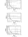
次に、この回路において抵抗器・サーミスタの抵抗値を以下のように設定する場合の温度補償の効果についてシミュレーションで得た結果をもとに説明する。なお、このシミュレーション時の電源電圧は2.8Vとした。各抵抗器は、R7を13.22kΩ、R8を153.64kΩ、R9を62.62kΩ、R11を11.66kΩ、R12を12.64kΩ、R13を22.20kΩ、とした。各サーミスタは25℃の温度での抵抗値が、TH1とTH4を470kΩ、TH2とTH5を0.68kΩ、TH3とTH6を68kΩと示すよう設定し、各サーミスタのB定数は、TH1とTH4が4650、TH2とTH5が4040、TH3とTH6が4650を示すものとした。 Next, the effect of temperature compensation when the resistance values of the resistors and thermistors are set as follows in this circuit will be described based on the results obtained by simulation. The power supply voltage during this simulation was 2.8V. Each resistor had R7 of 13.22 kΩ, R8 of 153.64 kΩ, R9 of 62.62 kΩ, R11 of 11.66 kΩ, R12 of 12.64 kΩ, and R13 of 22.20 kΩ. Each thermistor is set so that the resistance value at a temperature of 25 ° C. is 470 kΩ for TH1 and TH4, 0.68 kΩ for TH2 and TH5, and 68 kΩ for TH3 and TH6. The B constant of each thermistor is 4650 for TH1 and TH4. TH2 and TH5 indicate 4040, and TH3 and TH6 indicate 4650.
ここで図12にこれらのサーミスタの抵抗温度特性を示す。また、図13にこの回路の水晶発振子XD1の周波数温度特性を示す。 FIG. 12 shows the resistance temperature characteristics of these thermistors. FIG. 13 shows the frequency temperature characteristics of the crystal oscillator XD1 of this circuit.
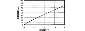
また、この回路における水晶振動子XD1およびバラクタダイオードVD1による共振周波数と、バラクタダイオードVD1の両端子の電位差との関係を、一定温度、0V印加の時を基準として図14に示す。 FIG. 14 shows the relationship between the resonance frequency of the crystal resonator XD1 and the varactor diode VD1 in this circuit and the potential difference between both terminals of the varactor diode VD1, with reference to a constant temperature and 0 V applied.
シミュレーションでは、それぞれの感温抵抗素子回路に含まれる抵抗器とサーミスタとを上記のように設定した。これによりサーミスタの温度に対する抵抗の変化により感温抵抗素子回路15aと感温抵抗素子回路15bとの出力電圧も温度により変動した。図15(a)に感温抵抗素子回路15aから出力される出力電圧、図15(b)に感温抵抗素子回路15bから出力される出力電圧をそれぞれ示す。 In the simulation, the resistors and thermistors included in each temperature-sensitive resistance element circuit were set as described above. As a result, the output voltage of the temperature-sensitive resistor element circuit 15a and the temperature-sensitive resistor element circuit 15b also fluctuated depending on the temperature due to a change in resistance with respect to the temperature of the thermistor. FIG. 15A shows an output voltage output from the temperature-sensitive resistance element circuit 15a, and FIG. 15B shows an output voltage output from the temperature-sensitive resistance element circuit 15b.
次に、感温抵抗素子回路15aの出力電圧と感温抵抗素子回路15bの出力電圧とをバラクタダイオードVD1の両端子に印加した。その際のバラクタダイオードVD1の両端にかかる電位差を図15(c)に示す。この電位差により、バラクタダイオードVD1のキャパシタンスが定まり、バラクタダイオードVD1と水晶振動子XD1との合成キャパシタンスにより、この温度補償圧電発振回路11の共振周波数が定まる。この共振周波数の周波数温度特性を従来例で示した温度補償共振回路1の共振周波数とともに図16(a)に示す。
Next, the output voltage of the temperature sensitive resistor element circuit 15a and the output voltage of the temperature sensitive resistor element circuit 15b were applied to both terminals of the varactor diode VD1. The potential difference applied to both ends of the varactor diode VD1 at that time is shown in FIG. The capacitance of the varactor diode VD1 is determined by this potential difference, and the resonance frequency of the temperature compensated
以上のように各感温抵抗素子回路の出力電圧と周波数とが、水晶発振子の周波数温度特性の描く3次曲線とは逆方向に変化する3次曲線を描き、水晶発振子の温度変化による周波数の変化を打ち消したことで、図16(a)のように、共振周波数の温度による変動を小さく安定したものにできた。本実施形態の回路においては、図16(a)のようにほとんど全体の温度域に亘って共振周波数を変動の小さなものとすることができ、さらに、従来は温度補償の設定が困難であった例えば60℃以上の温度域における周波数も調整可能となった。 As described above, the output voltage and frequency of each temperature-sensitive resistor element circuit draws a cubic curve that changes in the opposite direction to the cubic curve drawn by the frequency temperature characteristics of the crystal oscillator, and depends on the temperature change of the crystal oscillator. By canceling out the change in frequency, as shown in FIG. 16A, the fluctuation of the resonance frequency due to temperature can be made small and stable. In the circuit of this embodiment, as shown in FIG. 16A, the resonance frequency can be made small in variation over almost the entire temperature range, and it has been difficult to set temperature compensation in the past. For example, the frequency in a temperature range of 60 ° C. or higher can be adjusted.
ここで示したように感温抵抗素子回路15a・感温抵抗素子回路15bを上下反転させて接続し、感温抵抗素子回路15a・感温抵抗素子回路15bで同一の抵抗温度特性の定格サーミスタを使用することで、温度補償圧電発振回路11全体としての定格サーミスタの種類数を抑制できる。そのため、さらに各感温抵抗素子回路の出力電圧の計算が簡易になるとともに、容易に温度補償圧電発振回路の設計が行える。なお、このシミュレーションの例では同一の定格サーミスタをいくつか用いたが、同一の定格サーミスタを用いなくともよく、その場合にはより細かな温度補償の設定ができるとともに、従来では表現できなかった温度補償電圧の波形を実現できる。また、それぞれの定格サーミスタの位置が異なっていてもよく、1つの感温抵抗素子回路内で同一の定格サーミスタを複数用いなければどのように構成してもよい。
As shown here, the temperature sensitive resistor element circuit 15a and the temperature sensitive resistor element circuit 15b are connected upside down, and the rated thermistor having the same resistance temperature characteristic is used in the temperature sensitive resistor element circuit 15a and the temperature sensitive resistor element circuit 15b. By using it, the number of types of rated thermistors in the temperature compensated
また、このように比較的高い抵抗値のサーミスタのみで各感温抵抗素子回路を構成すると、各サーミスタの自己発熱を抑制することができ、回路全体としての消費電力も抑制することができる。 In addition, when each temperature-sensitive resistance element circuit is configured only by a thermistor having a relatively high resistance value, self-heating of each thermistor can be suppressed, and power consumption of the entire circuit can also be suppressed.
なお、ここで示したように同一の抵抗温度特性のサーミスタを各感温抵抗素子回路の対応する位置に用いなくともよく、その場合には、より温度補償の自由度が上がり、優れた温度補償を行うことができる。 As shown here, it is not necessary to use thermistors having the same resistance temperature characteristics at the corresponding positions of each temperature-sensitive resistance element circuit. In that case, the degree of freedom in temperature compensation is further increased and excellent temperature compensation is achieved. It can be performed.
また、電源電圧Vcc端子に電圧レギュレーターを介して接続すると電源電圧の変動の影響を軽減することができる。 Further, if the power supply voltage Vcc terminal is connected via a voltage regulator, the influence of fluctuations in the power supply voltage can be reduced.
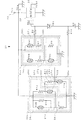
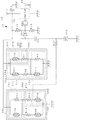
次に第2の実施形態の回路例を、図3に示す。 Next, FIG. 3 shows a circuit example of the second embodiment.
図3の温度補償圧電発振回路21は、圧電共振素子である水晶振動子XD1と、水晶振動子XD1の一方端に接続する増幅回路24と、水晶振動子XD1の他方端に接続する可変容量素子であるバラクタダイオードVD1を備える。ここで増幅回路24は前述の第1の実施形態の回路例で示した増幅回路14と同一のものである。
3 includes a crystal resonator XD1, which is a piezoelectric resonator, an
バラクタダイオードVD1のアノードは水晶振動子XD1と接続し、バラクタダイオードVD1のアノードにはさらに抵抗器R6を介して感温抵抗素子回路25aを接続している。また、バラクタダイオードVD1のカソードには抵抗器R10を介して感温抵抗素子回路25bを接続し、さらに直流電流遮断用のコンデンサC5を介して接地している。 The anode of the varactor diode VD1 is connected to the crystal resonator XD1, and the temperature-sensitive resistance element circuit 25a is further connected to the anode of the varactor diode VD1 via a resistor R6. Further, a temperature-sensitive resistance element circuit 25b is connected to the cathode of the varactor diode VD1 through a resistor R10, and further grounded through a capacitor C5 for cutting off DC current.
ここで感温抵抗素子回路25aは、前述の第1の実施形態の回路例で示した感温抵抗素子回路15aと同一のものである。 Here, the temperature sensitive resistance element circuit 25a is the same as the temperature sensitive resistance element circuit 15a shown in the circuit example of the first embodiment.
一方、感温抵抗素子回路25bは、感温抵抗素子である負特性のサーミスタTH4・サーミスタTH5・サーミスタTH6と抵抗器R11・抵抗器R12・抵抗器R13・抵抗器R14を備えている。サーミスタTH6・抵抗器R13・抵抗器R14からなる回路は分圧回路26cとして作用する。また、サーミスタTH5・抵抗器R12からなる回路は分圧回路26dとして作用する。また、サーミスタTH4・抵抗器R11からなる回路は分圧回路26eとして作用する。そのため、この感温抵抗素子回路25bは、分圧回路26cと分圧回路26dと分圧回路26eとによる3段の分圧を行う。 On the other hand, the temperature-sensitive resistance element circuit 25b includes a thermistor TH4, the thermistor TH5, the thermistor TH6, which are temperature-sensitive resistance elements, and a resistor R11, a resistor R12, a resistor R13, and a resistor R14. A circuit including the thermistor TH6, the resistor R13, and the resistor R14 functions as a voltage dividing circuit 26c. Further, a circuit composed of the thermistor TH5 and the resistor R12 functions as a voltage dividing circuit 26d. Further, the circuit composed of the thermistor TH4 and the resistor R11 acts as a voltage dividing circuit 26e. Therefore, the temperature-sensitive resistor element circuit 25b performs three-stage voltage division by the voltage divider circuit 26c, the voltage divider circuit 26d, and the voltage divider circuit 26e.
分圧回路26cでは、第1抵抗回路27cとしてサーミスタTH6・抵抗器R13を並列に接続し、この並列回路の一方端を電源電圧Vcc端子22に接続している。また、第2抵抗回路28cとして抵抗器R14を用い、抵抗器R14の一方端を接地している。そして、第1抵抗回路27cと第2抵抗回路28cを直列接続し、接続点を分圧回路26dに接続している。
In the voltage dividing circuit 26c, the thermistor TH6 and the resistor R13 are connected in parallel as the first resistance circuit 27c, and one end of the parallel circuit is connected to the power supply
分圧回路26dでは、第1抵抗回路27dである抵抗器R12の一方端を電源電圧Vcc端子22に接続している。また、第2抵抗回路28dであるサーミスタTH5の一方端を分圧回路26cの分圧点に接続している。そして、第1抵抗回路27dである抵抗器R12と第2抵抗回路28dであるサーミスタTH5とを直列接続し、接続点を分圧回路26eに接続している。
In the voltage dividing circuit 26d, one end of the resistor R12, which is the first resistance circuit 27d, is connected to the power supply
分圧回路26eでは、第1抵抗回路27eである抵抗器R11の一方端を分圧回路26dの分圧点に接続している。また、第2抵抗回路28eであるサーミスタTH4の一方端を接地している。そして、第1抵抗回路27eである抵抗器R11と第2抵抗回路28eであるサーミスタTH4とを直列接続し、接続点をバラクタダイオードVD1のカソードに抵抗器R10を介して接続している。 In the voltage dividing circuit 26e, one end of the resistor R11 which is the first resistance circuit 27e is connected to the voltage dividing point of the voltage dividing circuit 26d. Further, one end of the thermistor TH4 which is the second resistance circuit 28e is grounded. The resistor R11, which is the first resistor circuit 27e, and the thermistor TH4, which is the second resistor circuit 28e, are connected in series, and the connection point is connected to the cathode of the varactor diode VD1 via the resistor R10.
感温抵抗素子回路25bのように3つの分圧回路による3段の分圧を行う場合、従来は分圧回路間に増幅器を設けてダイナミックレンジを所定以上にする必要があった。しかし本実施形態の場合には、一方の感温抵抗素子回路25aを2段の分圧を行うものとすることで、この2段の分圧を行う感温抵抗素子回路25aにより必要なダイナミックレンジを確保する。感温抵抗素子回路25aを主として作用させ、3段の分圧を行う感温抵抗素子回路25bを補助的な微調整用に作用させることで、増幅器を分圧回路の間に設けなくても充分なダイナミックレンジを得ることができる。 In the case of performing three-stage voltage division by three voltage dividing circuits as in the temperature sensitive resistance element circuit 25b, it has been conventionally necessary to provide an amplifier between the voltage dividing circuits so that the dynamic range is not less than a predetermined value. However, in the case of the present embodiment, one of the temperature-sensitive resistance element circuits 25a performs voltage division in two stages, so that a dynamic range required by the temperature-sensitive resistance element circuit 25a that performs voltage division in two stages is required. Secure. The temperature-sensitive resistor element circuit 25a mainly operates and the temperature-sensitive resistor element circuit 25b that performs three-stage voltage division is used for auxiliary fine adjustment, so that an amplifier is not provided between the voltage-dividing circuits. Dynamic range can be obtained.
なお、本実施形態の回路構成例では感温抵抗素子回路25aを第1の実施形態での感温抵抗素子回路15aと同一なものとしたが、他の感温抵抗素子回路でもよく、例えば感温抵抗素子回路15bや、感温抵抗素子回路25bや、感温抵抗素子回路25bを上下反転させたものとしてもよく。少なくとも1つの感温抵抗素子回路が3段の分圧を行うと同様な効果を奏する。 In the circuit configuration example of this embodiment, the temperature-sensitive resistor element circuit 25a is the same as the temperature-sensitive resistor element circuit 15a in the first embodiment, but other temperature-sensitive resistor element circuits may be used. The temperature resistance element circuit 15b, the temperature sensing resistance element circuit 25b, and the temperature sensing resistance element circuit 25b may be vertically inverted. When at least one temperature-sensitive resistance element circuit performs three-stage voltage division, the same effect is obtained.
次に第3の実施形態の回路例を図4に示す。 Next, FIG. 4 shows a circuit example of the third embodiment.
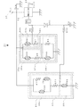
図4の温度補償圧電発振回路31は、圧電共振素子である水晶振動子XD1と、水晶振動子XD1の一方端に接続する増幅回路34と、水晶振動子XD1の他方端に接続する可変容量素子であるバラクタダイオードVD1を備える。ここで増幅回路34は前述の第2の実施形態の回路例で示した増幅回路24と同一のものである。
4 includes a crystal resonator XD1, which is a piezoelectric resonance element, an
バラクタダイオードVD1のアノードは水晶振動子XD1と接続し、バラクタダイオードVD1のアノードにはさらに抵抗器R6を介して感温抵抗素子回路35aを接続している。また、バラクタダイオードVD1のカソードには抵抗器R10を介して感温抵抗素子回路35bを接続し、さらに直流電流遮断用のコンデンサC5を介して接地している。 The anode of the varactor diode VD1 is connected to the crystal resonator XD1, and the temperature sensitive resistance element circuit 35a is further connected to the anode of the varactor diode VD1 via a resistor R6. Further, a temperature-sensitive resistance element circuit 35b is connected to the cathode of the varactor diode VD1 through a resistor R10, and further grounded through a capacitor C5 for cutting off direct current.
ここで感温抵抗素子回路35aは、前述の第2の実施形態の回路例で示した感温抵抗素子回路25aと同一のものである。 Here, the temperature-sensitive resistance element circuit 35a is the same as the temperature-sensitive resistance element circuit 25a shown in the circuit example of the second embodiment described above.
一方、感温抵抗素子回路35bは、感温抵抗素子である負特性のサーミスタTH4・サーミスタTH5・サーミスタTH6と抵抗器R11・抵抗器R12を備えている。すると、このサーミスタTH4・サーミスタTH5・サーミスタTH6・抵抗器R11・抵抗器R12が分圧回路36cとして作用する。そのため、この感温抵抗素子回路35bは、分圧回路36cによる一段の分圧を行う。
On the other hand, the temperature-sensitive resistor element circuit 35b includes a thermistor TH4, thermistor TH5, thermistor TH6, and resistors R11 and R12, which are temperature-sensitive resistors. Then, the thermistor TH4, the thermistor TH5, the thermistor TH6, the resistor R11, and the resistor R12 act as the
この分圧回路36cでは、第1抵抗回路37cとしてサーミスタTH4・抵抗器R12を直列に接続し、この直列回路をサーミスタTH5と並列に接続し、さらにその並列回路の一方端に抵抗器R11を直列に接続している。そしてサーミスタTH4・抵抗器R12とサーミスタTH5とから成る並列回路の、抵抗器R12の側の端子を電源電圧Vcc端子32に接続している。また、第2抵抗回路38cとしてサーミスタTH6を用い、サーミスタTH6の一方端を接地している。そして、第1抵抗回路37cの抵抗器R11の一方端と第2抵抗回路38cであるサーミスタTH6の一方端とを直列接続し、接続点をバラクタダイオードVD1のカソードに抵抗器R10を介して接続している。
In the
このように感温抵抗素子回路35bを、1段の分圧を行うものとした場合でも感温抵抗素子回路35aの2段の分圧を行う感温抵抗素子回路35bとともに用いることで、従来より高精度な温度補償電圧の設定とサーミスタの種類の数の抑制をすることができる。そして、1段の分圧回路36cしか備えない感温抵抗素子回路35bによって出力電圧のダイナミックレンジを大きくとることができる。
As described above, even when the temperature-sensitive resistance element circuit 35b is used to perform one-stage voltage division, the temperature-sensitive resistance element circuit 35b is used together with the temperature-sensitive resistance element circuit 35b that performs the two-stage voltage division. A highly accurate temperature compensation voltage can be set and the number of thermistor types can be reduced. The dynamic range of the output voltage can be increased by the temperature sensitive resistance element circuit 35b having only one stage
なお、本実施形態の回路構成例では感温抵抗素子回路35aを第2の実施形態での感温抵抗素子回路25aと同一なものとしたが、他の感温抵抗素子回路でもよく、例えば感温抵抗素子回路15bや、感温抵抗素子回路25bや、感温抵抗素子回路25bを上下反転させたものとしてもよく。少なくとも1つの感温抵抗素子回路が1段の分圧を行い、他の一つの感温抵抗素子回路が2段以上の分圧を行うと同様な効果を奏する。 In the circuit configuration example of this embodiment, the temperature-sensitive resistor element circuit 35a is the same as the temperature-sensitive resistor element circuit 25a in the second embodiment, but other temperature-sensitive resistor element circuits may be used. The temperature resistance element circuit 15b, the temperature sensing resistance element circuit 25b, and the temperature sensing resistance element circuit 25b may be vertically inverted. When at least one temperature-sensitive resistance element circuit performs one-stage voltage division and another one temperature-sensitive resistance element circuit performs voltage division of two or more stages, the same effect is obtained.
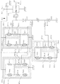
次に第4の実施形態の回路例を、図5に示す。 Next, FIG. 5 shows a circuit example of the fourth embodiment.
図5の温度補償圧電発振回路41は、圧電共振素子である水晶振動子XD1と、水晶振動子XD1の一方端に接続する増幅回路44と、水晶振動子XD1の他方端に接続する可変容量素子であるバラクタダイオードVD1を備える。
The temperature compensated piezoelectric oscillation circuit 41 in FIG. 5 includes a crystal resonator XD1, which is a piezoelectric resonance element, an
バラクタダイオードVD1のアノードは水晶振動子XD1と接続し、バラクタダイオードVD1のアノードにはさらに抵抗器R6を介して感温抵抗素子回路45aを接続している。また、バラクタダイオードVD1のカソードには抵抗器R10を介して感温抵抗素子回路45bを接続し、さらに直流電流遮断用のコンデンサC5を介して接地している。 The anode of the varactor diode VD1 is connected to the crystal resonator XD1, and the temperature-sensitive resistance element circuit 45a is further connected to the anode of the varactor diode VD1 via a resistor R6. Further, a temperature-sensitive resistance element circuit 45b is connected to the cathode of the varactor diode VD1 through a resistor R10, and further grounded through a capacitor C5 for cutting off a direct current.
ここで増幅回路44は前述の第3の実施形態の回路例で示した増幅回路34と同一のものである。また感温抵抗素子回路45aは、感温抵抗素子回路35aと同一のものである。
Here, the
一方、感温抵抗素子回路45bは、感温抵抗素子であるサーミスタTH4・サーミスタTH5・サーミスタTH6・サーミスタTH7と抵抗器R11・抵抗器R12・抵抗器R13・抵抗器R14を備えている。サーミスタTH6・サーミスタTH7・抵抗器R13・抵抗器R14からなる回路は分圧回路46cとして作用する。また、サーミスタTH5・抵抗器R12からなる回路は分圧回路46dとして作用する。また、サーミスタTH4・抵抗器R11からなる回路は分圧回路46eとして作用する。そのため、この感温抵抗素子回路45bは、分圧回路46cと分圧回路46dと分圧回路46eとによる3段の分圧を行う。
On the other hand, the temperature sensitive resistor element circuit 45b includes a thermistor TH4, the thermistor TH5, the thermistor TH6, the thermistor TH7, and the resistors R11, R12, R13, and R14 which are temperature sensitive resistors. A circuit comprising the thermistor TH6, the thermistor TH7, the resistor R13, and the resistor R14 functions as a voltage dividing circuit 46c. Further, a circuit composed of the thermistor TH5 and the resistor R12 functions as a
分圧回路46cでは、第1抵抗回路47cとしてサーミスタTH6・抵抗器R13を並列に接続し、この並列回路の一方端を電源電圧Vcc端子42に接続している。また、第2抵抗回路48cとして抵抗器R14とサーミスタTH7を接続し、サーミスタTH7の一方端を接地している。そして、第1抵抗回路47cと第2抵抗回路48cを直列接続し、接続点を分圧回路46dに接続している。
In the voltage dividing circuit 46c, the thermistor TH6 and the resistor R13 are connected in parallel as the first resistance circuit 47c, and one end of the parallel circuit is connected to the power supply voltage Vcc terminal 42. Further, the resistor R14 and the thermistor TH7 are connected as the second resistance circuit 48c, and one end of the thermistor TH7 is grounded. The first resistor circuit 47c and the second resistor circuit 48c are connected in series, and the connection point is connected to the
分圧回路46dでは、第1抵抗回路47dである抵抗器R12の一方端を分圧回路46cの分圧点に接続している。また、第2抵抗回路48dであるサーミスタTH5の一方端を接地している。そして、第1抵抗回路47dである抵抗器R12と第2抵抗回路48dであるサーミスタTH5とを直列接続し、接続点を分圧回路46eに接続している。
In the
分圧回路46eでは、第1抵抗回路47eである抵抗器R11の一方端を電源電圧Vcc端子42に接続している。また、第2抵抗回路48eであるサーミスタTH4の一方端を分圧回路46dの分圧点に接続している。そして、第1抵抗回路47eである抵抗器R11と第2抵抗回路48eであるサーミスタTH4とを直列接続し、接続点をバラクタダイオードVD1のカソードに抵抗器R10を介して接続している。
In the voltage dividing circuit 46e, one end of the resistor R11 which is the first resistance circuit 47e is connected to the power supply voltage Vcc terminal 42. Further, one end of the thermistor TH4 which is the second resistance circuit 48e is connected to the voltage dividing point of the
このように3つの分圧回路による3段の分圧を行い、さらに4つのサーミスタを1つの感温抵抗素子回路に設けた場合でも、従来のように増幅器を設けなくとも、一方の感温抵抗素子回路45aを2段の分圧を行うものとすることで、必要なダイナミックレンジを確保する。感温抵抗素子回路45aを主として作用させ、3段の分圧を行う感温抵抗素子回路45bを補助的な微調整用に作用させることで、増幅器を分圧回路の間に設けなくとも充分なダイナミックレンジを得ることができる。そして、この4つのサーミスタにより更に高精度に温度補償の設定ができ、より多くの感温抵抗素子により優れた温度補償を行うことができる。 Thus, even when four thermistors are provided in one temperature-sensitive resistance element circuit by performing three-stage voltage division by three voltage-dividing circuits, one temperature-sensitive resistor can be provided without providing an amplifier as in the prior art. The element circuit 45a performs voltage division in two stages, thereby securing a necessary dynamic range. The temperature-sensitive resistor element circuit 45a mainly operates and the temperature-sensitive resistor element circuit 45b that performs three-stage voltage division is used for auxiliary fine adjustment, so that it is sufficient even if an amplifier is not provided between the voltage-dividing circuits. A dynamic range can be obtained. The four thermistors can set temperature compensation with higher accuracy, and more temperature-sensitive resistance elements can perform excellent temperature compensation.
なお、本実施形態の回路構成例では感温抵抗素子回路45aを第3の実施形態での感温抵抗素子回路35aと同一なものとしたが、他の感温抵抗素子回路でもよく、例えば感温抵抗素子回路15bや、感温抵抗素子回路25bや、感温抵抗素子回路25bを上下反転させたもの、感温抵抗素子回路35bや、感温抵抗素子回路35bを上下反転させたもの、感温抵抗素子回路45bを上下反転させたものとしてもよく。少なくとも1つの感温抵抗素子回路が3段以上の分圧を行い、さらに4つ以上のサーミスタをその感温抵抗素子回路に設けた場合でも同様な効果を奏する。なお、従来の例で示した回路では増幅器を設けずに4つ以上のサーミスタで1つの分圧回路を構成することは温度補償電圧の設計上困難である。 In the circuit configuration example of this embodiment, the temperature-sensitive resistor element circuit 45a is the same as the temperature-sensitive resistor element circuit 35a in the third embodiment, but other temperature-sensitive resistor element circuits may be used. Temperature resistance element circuit 15b, temperature sensing resistance element circuit 25b, temperature sensing resistance element circuit 25b upside down, temperature sensing resistance element circuit 35b, temperature sensing resistance element circuit 35b upside down, The temperature resistance element circuit 45b may be turned upside down. Even when at least one temperature-sensitive resistance element circuit performs voltage division of three or more stages and four or more thermistors are provided in the temperature-sensitive resistance element circuit, the same effect can be obtained. In the circuit shown in the conventional example, it is difficult to design a temperature compensation voltage by configuring one voltage dividing circuit with four or more thermistors without providing an amplifier.
次に第5の実施形態の回路例を、図6に示す。 Next, FIG. 6 shows a circuit example of the fifth embodiment.
図6の温度補償圧電発振回路51は、圧電共振素子である水晶振動子XD1と、水晶振動子XD1の一方端に接続する増幅回路54と、水晶振動子XD1の他方端に接続する複数の可変容量素子であるバラクタダイオードVD1・バラクタダイオードVD2を備える。
The temperature compensated
バラクタダイオードVD1のカソードは水晶振動子XD1と接続し、水晶振動子XD1と接続されたバラクタダイオードVD1のカソードは、バイアス回路である抵抗器R13・抵抗器R14と接続し、抵抗器R13を介して電源電圧Vcc端子52と接続し、抵抗器R14を介して接地することでカソード電圧を設定している。 The cathode of the varactor diode VD1 is connected to the crystal resonator XD1, and the cathode of the varactor diode VD1 connected to the crystal resonator XD1 is connected to the resistor R13 and the resistor R14 which are bias circuits, via the resistor R13. The cathode voltage is set by connecting to the power supply voltage Vcc terminal 52 and grounding via the resistor R14.
そして、バラクタダイオードVD1のアノードには抵抗器R6を介して感温抵抗素子回路55aを接続している。また、バラクタダイオードVD1のアノードにはさらに直流電流遮断用のコンデンサC6の一方端を接続している。コンデンサC6の他方端には抵抗器R10を介して感温抵抗素子回路55bを接続している。また、コンデンサC6の前記他方端にはさらにバラクタダイオードVD2のカソードを接続している。バラクタダイオードVD2のアノードは接地している。 A temperature-sensitive resistance element circuit 55a is connected to the anode of the varactor diode VD1 via a resistor R6. The anode of the varactor diode VD1 is further connected to one end of a DC current blocking capacitor C6. A temperature sensitive resistance element circuit 55b is connected to the other end of the capacitor C6 via a resistor R10. Further, the cathode of the varactor diode VD2 is further connected to the other end of the capacitor C6. The anode of the varactor diode VD2 is grounded.
ここで増幅回路54は前述の第1の実施形態の回路例で示した増幅回路14と同一のものである。また感温抵抗素子回路55aと感温抵抗素子回路55bとは、それぞれ感温抵抗素子回路15a・感温抵抗素子回路15bと同一のものである。
Here, the
このように2つ感温抵抗素子回路で温度補償圧電発振回路を構成し、バラクタダイオードVD1・バラクタダイオードVD2のキャパシタンスにより水晶発振子XD1との合成キャパシタンスを変化させ、共振周波数を調整可能としている。 In this way, a temperature compensated piezoelectric oscillation circuit is constituted by two temperature sensitive resistance element circuits, and the combined capacitance with the crystal oscillator XD1 is changed by the capacitances of the varactor diode VD1 and the varactor diode VD2, so that the resonance frequency can be adjusted.
このように、バラクタダイオードVD1のアノードに感温抵抗素子回路55aを、バラクタダイオードVD2のカソードに感温抵抗素子回路55bを接続しているため、バラクタダイオードVD1・バラクタダイオードVD2への印加電圧の設定を個別に行うことができ、設計に際して個別の感温抵抗素子回路の設計の自由度が向上する。特に、例えばバラクタダイオードVD1とバラクタダイオードVD2に印加電圧に対する容量変化の異なるものを用いると、一方のバラクタダイオードに電圧を印加する感温抵抗素子回路で粗い温度補償を行い、他方のバラクタダイオードに電圧を印加する感温抵抗素子回路で細かい温度補償を行うことが可能になる。 In this way, since the temperature sensitive resistor element circuit 55a is connected to the anode of the varactor diode VD1, and the temperature sensitive resistor element circuit 55b is connected to the cathode of the varactor diode VD2, the voltage applied to the varactor diode VD1 and the varactor diode VD2 is set. Thus, the degree of freedom in designing individual temperature-sensitive resistance element circuits can be improved. In particular, for example, when a varactor diode VD1 and a varactor diode VD2 having different capacitance changes with respect to the applied voltage are used, rough temperature compensation is performed by a temperature-sensitive resistance element circuit that applies a voltage to one varactor diode, and a voltage is applied to the other varactor diode. It becomes possible to perform fine temperature compensation with the temperature-sensitive resistance element circuit to which the voltage is applied.
なお、本実施形態の回路構成例では感温抵抗素子回路55a・感温抵抗素子回路55bを第1の実施形態での感温抵抗素子回路15a・感温抵抗素子回路15aと同一なものとしたが、それぞれ他の感温抵抗素子回路でもよく、例えば感温抵抗素子回路25aや、感温抵抗素子回路25aを上下反転させたもの、感温抵抗素子回路25bや、感温抵抗素子回路25bを上下反転させたもの、感温抵抗素子回路35bや、感温抵抗素子回路35bを上下反転させたもの、感温抵抗素子回路45bや、感温抵抗素子回路45bを上下反転させたものとしてもよい。複数のバラクタダイオードの端子にそれぞれの感温抵抗素子回路を設けさえすれば同様な効果を奏する。 In the circuit configuration example of the present embodiment, the temperature-sensitive resistor element circuit 55a and the temperature-sensitive resistor element circuit 55b are the same as the temperature-sensitive resistor element circuit 15a and the temperature-sensitive resistor element circuit 15a in the first embodiment. However, other temperature-sensitive resistance element circuits may be used. For example, the temperature-sensitive resistance element circuit 25a, the one obtained by inverting the temperature-sensitive resistance element circuit 25a, the temperature-sensitive resistance element circuit 25b, or the temperature-sensitive resistance element circuit 25b may be used. It may be a vertically inverted one, a temperature sensitive resistor element circuit 35b, a temperature sensitive resistor element circuit 35b vertically inverted, a temperature sensitive resistor element circuit 45b, or a temperature sensitive resistor element circuit 45b inverted vertically. . As long as each temperature-sensitive resistance element circuit is provided at the terminals of a plurality of varactor diodes, the same effect is obtained.
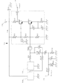
次に第6の実施形態の回路例を、図7に示す。 Next, FIG. 7 shows a circuit example of the sixth embodiment.
図7の温度補償圧電発振回路61は、圧電共振素子である水晶振動子XD1と、水晶振動子XD1の一方端に接続する増幅回路64と、水晶振動子XD1の他方端に接続する複数の可変容量素子(バラクタダイオードVD1・バラクタダイオードVD2)を備える。 The temperature compensated piezoelectric oscillation circuit 61 in FIG. 7 includes a crystal resonator XD1, which is a piezoelectric resonance element, an amplifier circuit 64 connected to one end of the crystal resonator XD1, and a plurality of variable terminals connected to the other end of the crystal resonator XD1. Capacitance elements (varactor diodes VD1 and varactor diodes VD2) are provided.
バラクタダイオードVD1のアノードは水晶振動子XD1と接続し、バラクタダイオードVD1のアノードにはさらに抵抗器R6を介して感温抵抗素子回路65aを接続する。バラクタダイオードVD1のカソードには抵抗器R14を介して感温抵抗素子回路65cを接続する。また、バラクタダイオードVD1のカソードにはさらに直流電流遮断用のコンデンサC6の一方端を接続する。コンデンサC6の他方端にはバラクタダイオードVD2のカソードを接続する。バラクタダイオードVD2のカソードにはさらに、抵抗器R10を介して感温抵抗素子回路65bを接続する。バラクタダイオードVD2のアノードは接地する。 The anode of the varactor diode VD1 is connected to the crystal resonator XD1, and the temperature-sensitive resistance element circuit 65a is further connected to the anode of the varactor diode VD1 through a resistor R6. A temperature sensitive resistor element circuit 65c is connected to the cathode of the varactor diode VD1 through a resistor R14. Further, one end of a DC current blocking capacitor C6 is further connected to the cathode of the varactor diode VD1. The other end of the capacitor C6 is connected to the cathode of the varactor diode VD2. A temperature sensitive resistance element circuit 65b is further connected to the cathode of the varactor diode VD2 via a resistor R10. The anode of the varactor diode VD2 is grounded.
ここで増幅回路64は前述の第5の実施形態の回路例で示した増幅回路54と同一のものである。また感温抵抗素子回路65aは感温抵抗素子回路55aと同一のものであり、感温抵抗素子回路65b・感温抵抗素子回路65cは、感温抵抗素子回路55bと同一のものであり、感温抵抗素子回路65cは感温抵抗素子回路65bのサーミスタと抵抗器との記号を変えたものである。
Here, the amplifier circuit 64 is the same as the
このように3つの感温抵抗素子回路で温度補償圧電発振回路を構成し、バラクタダイオードVD1・バラクタダイオードVD2のキャパシタンスにより水晶発振子XD1との合成キャパシタンスを変化させ、共振周波数を調整可能としている。また、このように感温抵抗素子回路の接続数を増やすことで感温抵抗素子回路を更に多く設けることができ、更に精緻に温度補償電圧を形成することができる。 In this way, a temperature-compensated piezoelectric oscillation circuit is constituted by the three temperature-sensitive resistance element circuits, and the combined capacitance with the crystal resonator XD1 is changed by the capacitances of the varactor diode VD1 and the varactor diode VD2, so that the resonance frequency can be adjusted. Further, by increasing the number of connections of the temperature sensitive resistance element circuit in this way, more temperature sensitive resistance element circuits can be provided, and the temperature compensation voltage can be formed more precisely.
また、バラクタダイオードVD1ではその両端子に感温抵抗素子回路を接続し、バラクタダイオードVD2ではその端子のうち一方の端子にのみ感温抵抗素子回路を接続しているため、バラクタダイオードVD1では両端子間の電位差をより自由に設定することができ、たとえば電源電圧を低電圧に設定した場合であっても容易に電位差の設定を行うことができる。 Further, since the temperature sensitive resistance element circuit is connected to both terminals of the varactor diode VD1, and the temperature sensitive resistance element circuit is connected to only one of the terminals of the varactor diode VD2, both terminals of the varactor diode VD1 are connected. The potential difference can be set more freely. For example, even when the power supply voltage is set to a low voltage, the potential difference can be easily set.
なお、本実施形態の回路構成例では感温抵抗素子回路65a・感温抵抗素子回路65b・感温抵抗素子回路65cを第5の実施形態での感温抵抗素子回路55aや感温抵抗素子回路55bと同一なものとしたが、他の感温抵抗素子回路でもよく、例えば感温抵抗素子回路15bや、感温抵抗素子回路15bを上下反転させたもの、感温抵抗素子回路25bや、感温抵抗素子回路25bを上下反転させたもの、感温抵抗素子回路35bや、感温抵抗素子回路35bを上下反転させたもの、感温抵抗素子回路45bや、感温抵抗素子回路45bを上下反転させたものとしてもよい。3つ以上の感温抵抗素子回路を設けさえすれば同様な効果を奏する。 In the circuit configuration example of this embodiment, the temperature-sensitive resistor element circuit 65a, the temperature-sensitive resistor element circuit 65b, and the temperature-sensitive resistor element circuit 65c are replaced with the temperature-sensitive resistor element circuit 55a and the temperature-sensitive resistor element circuit in the fifth embodiment. However, other temperature-sensitive resistor element circuits may be used. For example, the temperature-sensitive resistor element circuit 15b, the temperature-sensitive resistor element circuit 15b upside down, the temperature-sensitive resistor element circuit 25b, The thermal resistance element circuit 25b is inverted upside down, the temperature sensitive resistance element circuit 35b, the temperature sensitive resistance element circuit 35b is inverted upside down, the temperature sensitive resistance element circuit 45b, and the temperature sensitive resistance element circuit 45b are inverted upside down. It is good also as what was made to do. As long as three or more temperature-sensitive resistance element circuits are provided, the same effect can be obtained.
次に第7の実施形態を、図8に示す。 Next, a seventh embodiment is shown in FIG.
図8の温度補償圧電発振回路71は、圧電共振素子である水晶振動子XD1と、水晶振動子XD1の一方端に接続するコルピッツ発振回路の負性抵抗発生部分である増幅回路74と、水晶振動子XD1の他方端に接続する複数の可変容量素子(バラクタダイオードVD1・バラクタダイオードVD2)を備える。
A temperature compensated
増幅回路74では、水晶振動子XD1をトランジスタQ1のベースに接続している。また、トランジスタQ1のコレクタをトランジスタQ2のエミッタと接続し、トランジスタQ1のエミッタは抵抗器R1およびコンデンサC2を介して接地している。また、トランジスタQ1のエミッタとベースとの間には、帰還用コンデンサC1を接続し、トランジスタQ1とトランジスタQ2のベースには抵抗器R5・抵抗器R3・抵抗器R2によるベースバイアス回路を接続している。
In the
またトランジスタQ2のベースは、コンデンサC8を介して高周波的に接地し、コレクタは、負荷抵抗である抵抗器R4を介して電源電圧Vcc端子72に接続し、コンデンサC3を介して信号出力Vout端子73に接続している。また、電源電圧Vcc端子72はコンデンサC4を介して高周波的に接地している。この結果、トランジスタQ1は水晶振動子XD1の共振周波数で負性抵抗回路として作用し、トランジスタQ2は、そのバッファ回路として作用する。 The base of the transistor Q2 is grounded in high frequency via a capacitor C8, the collector is connected to the power supply voltage Vcc terminal 72 via a resistor R4, which is a load resistance, and the signal output Vout terminal 73 is connected via a capacitor C3. Connected to. The power supply voltage Vcc terminal 72 is grounded at a high frequency via a capacitor C4. As a result, the transistor Q1 acts as a negative resistance circuit at the resonance frequency of the crystal resonator XD1, and the transistor Q2 acts as its buffer circuit.
このトランジスタQ2によるバッファ回路は、信号出力Vout端子73の負荷変動の影響を軽減し安定な発振の継続を図るものである。 This buffer circuit by the transistor Q2 reduces the influence of the load fluctuation of the signal output Vout terminal 73 and continues stable oscillation.
バラクタダイオードVD1のアノードは水晶振動子XD1と接続する。また、バラクタダイオードVD1には周波数感度を調整するためのコンデンサC7を並列に接続しており、このコンデンサC7のキャパシタンスの設定によりバラクタダイオードVD1の周波数感度を調整し、優れた温度補償を行うことができる。 The anode of the varactor diode VD1 is connected to the crystal unit XD1. In addition, a capacitor C7 for adjusting the frequency sensitivity is connected in parallel to the varactor diode VD1, and the frequency sensitivity of the varactor diode VD1 is adjusted by setting the capacitance of the capacitor C7 to perform excellent temperature compensation. it can.
さらにバラクタダイオードVD1のアノードには抵抗器R6を介して感温抵抗素子回路75aを接続する。カソードには抵抗器R10を介して感温抵抗素子回路75bを接続する。ここで、この感温抵抗素子回路75aは、前述の第6の実施形態で示した感温抵抗素子回路65aと同一のものであり、感温抵抗素子回路75bは、感温抵抗素子回路65bと同一のものである。 Furthermore, a temperature sensitive resistance element circuit 75a is connected to the anode of the varactor diode VD1 via a resistor R6. A temperature sensitive resistance element circuit 75b is connected to the cathode via a resistor R10. Here, the temperature-sensitive resistance element circuit 75a is the same as the temperature-sensitive resistance element circuit 65a shown in the sixth embodiment, and the temperature-sensitive resistance element circuit 75b is the same as the temperature-sensitive resistance element circuit 65b. Are the same.
また、バラクタダイオードVD1のカソードにはさらにそれぞれのバラクタダイオード間の直流電圧遮断用のコンデンサC6を介してバラクタダイオードVD2のカソードを接続している。このバラクタダイオードVD2のカソードにはさらに抵抗器R19を介して制御電圧Vcont端子79を接続している。バラクタダイオードVD2のアノードは接地している。このバラクタダイオードVD2には感度調整用のコンデンサC9と抵抗器R18を接続している。
The cathode of the varactor diode VD1 is further connected to the cathode of the varactor diode VD2 via a capacitor C6 for cutting off the DC voltage between the varactor diodes. A control
このコンデンサC9はバラクタダイオードVD2の周波数電圧感度を調整するためのコンデンサである。そのためコンデンサC9のキャパシタンスの設定によりバラクタダイオードVD2の周波数電圧感度を調整することができる。 The capacitor C9 is a capacitor for adjusting the frequency voltage sensitivity of the varactor diode VD2. Therefore, the frequency voltage sensitivity of the varactor diode VD2 can be adjusted by setting the capacitance of the capacitor C9.
制御電圧Vcont端子79を設けているため、制御電圧Vcontの制御により、このバラクタダイオードVD2のキャパシタンスが制御可能になる。
Since the control
このような構成により、複数の感温抵抗素子回路からの出力電圧によりバラクタダイオードVD1のキャパシタンスを変化させ、バラクタダイオードVD2への制御電圧の印加によりバラクタダイオードVD2のキャパシタンスを変化させ、それらのキャパシタンスにより水晶振動子XD1との合成キャパシタンスを変化させ、温度補償圧電発振回路71の共振周波数を調整可能としている。
With such a configuration, the capacitance of the varactor diode VD1 is changed by the output voltages from the plurality of temperature-sensitive resistance element circuits, and the capacitance of the varactor diode VD2 is changed by applying the control voltage to the varactor diode VD2. The resonance frequency of the temperature compensated
この構成による温度補償圧電発振回路71のシミュレーション結果の周波数温度特性を図16(b)に示す。図16(b)で示されたようにこの構成では、例えば10〜70℃の温度域で30ppb以下の優れた温度特性を得ることができる。
FIG. 16B shows the frequency temperature characteristic of the simulation result of the temperature compensated
なお、本実施形態の回路構成例では感温抵抗素子回路75a・感温抵抗素子回路75bを第6の実施形態での感温抵抗素子回路65aや感温抵抗素子回路65bと同一なものとしたが、他の感温抵抗素子回路でもよく、例えば感温抵抗素子回路15bや、感温抵抗素子回路15bを上下反転させたもの、感温抵抗素子回路25bや、感温抵抗素子回路25bを上下反転させたもの、感温抵抗素子回路35bや、感温抵抗素子回路35bを上下反転させたもの、感温抵抗素子回路45bや、感温抵抗素子回路45bを上下反転させたものとしてもよい。感温抵抗素子回路以外の部分の構成を類似な構成とすることにより本実施形態と同様な効果を奏するが、他の実施形態で示したような構成を部分的に適用してもよい。 In the circuit configuration example of this embodiment, the temperature-sensitive resistance element circuit 75a and the temperature-sensitive resistance element circuit 75b are the same as the temperature-sensitive resistance element circuit 65a and the temperature-sensitive resistance element circuit 65b in the sixth embodiment. However, other temperature-sensitive resistor element circuits may be used. For example, the temperature-sensitive resistor element circuit 15b or the temperature-sensitive resistor element circuit 15b is turned upside down, the temperature-sensitive resistor element circuit 25b, or the temperature-sensitive resistor element circuit 25b is moved up and down. It may be inverted, the temperature-sensitive resistor element circuit 35b, the temperature-sensitive resistor element circuit 35b turned upside down, the temperature-sensitive resistor element circuit 45b, or the temperature-sensitive resistor element circuit 45b turned upside down. Although the same effect as that of the present embodiment is obtained by making the configuration of the parts other than the temperature sensitive resistance element circuit similar, the configuration as shown in the other embodiments may be partially applied.
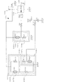
次に第8の実施形態の回路例を、図9に示す。 Next, FIG. 9 shows a circuit example of the eighth embodiment.
図9の温度補償圧電発振回路81は、圧電共振素子である水晶振動子XD1と、水晶振動子XD1の一方端に接続する増幅回路84と、水晶振動子XD1の他方端に接続する可変容量素子(バラクタダイオードVD1)を備える。
The temperature compensated piezoelectric oscillation circuit 81 in FIG. 9 includes a crystal resonator XD1 which is a piezoelectric resonance element, an
バラクタダイオードVD1のアノードは水晶振動子XD1と接続し、バラクタダイオードVD1のアノードにはさらに抵抗器R6を介して感温抵抗素子回路85aを接続する。バラクタダイオードVD1のカソードには抵抗器R10を介して感温抵抗素子回路85bを接続し、さらに直流電流遮断用のコンデンサC5を介して接地している。 The anode of the varactor diode VD1 is connected to the crystal resonator XD1, and the temperature-sensitive resistance element circuit 85a is further connected to the anode of the varactor diode VD1 via the resistor R6. A temperature-sensitive resistance element circuit 85b is connected to the cathode of the varactor diode VD1 through a resistor R10, and further grounded through a capacitor C5 for cutting off a direct current.
ここで増幅回路84は前述の第7の実施形態の回路例で示した増幅回路74と同一のものである。また感温抵抗素子回路85bは前述の第3の実施形態の回路例で示した感温抵抗素子回路35bと同一のものである。
Here, the
また、感温抵抗素子回路85aは、負特性のサーミスタTH1と、抵抗器R7・抵抗器R8・抵抗器R9を備えている。このサーミスタTH1・抵抗器R7・抵抗器R8・抵抗器R9からなる回路は分圧回路86aとして作用する。そのため、この感温抵抗素子回路85aは、分圧回路86aによる1段の分圧を行う。 The temperature-sensitive resistance element circuit 85a includes a thermistor TH1 having a negative characteristic, a resistor R7, a resistor R8, and a resistor R9. The circuit comprising the thermistor TH1, resistor R7, resistor R8, and resistor R9 acts as a voltage dividing circuit 86a. Therefore, the temperature-sensitive resistance element circuit 85a performs one-stage voltage division by the voltage dividing circuit 86a.
分圧回路86aでは第1抵抗回路87aとして、サーミスタTH1と抵抗器R7と並列に接続しこの並列回路の一方端を電源電圧Vcc端子82に接続している。また、他方端に抵抗器R8を接続している。この第1抵抗回路87aを第2抵抗回路88aである抵抗器R9に直列接続している。また、抵抗器R9の一方端を接地している。そして、第1抵抗回路87aと第2抵抗回路88aの接続点をバラクタダイオードVD1のアノードに抵抗器R6を介して接続している。 In the voltage dividing circuit 86a, as the first resistance circuit 87a, the thermistor TH1 and the resistor R7 are connected in parallel, and one end of the parallel circuit is connected to the power supply voltage Vcc terminal 82. A resistor R8 is connected to the other end. The first resistor circuit 87a is connected in series to a resistor R9 which is a second resistor circuit 88a. Further, one end of the resistor R9 is grounded. The connection point between the first resistor circuit 87a and the second resistor circuit 88a is connected to the anode of the varactor diode VD1 via the resistor R6.
このように2つの感温抵抗素子回路85a・感温抵抗素子回路85bで温度補償圧電発振回路81を構成し、バラクタダイオードVD1のキャパシタンスにより水晶発振子XD1との合成キャパシタンスを変化させ、共振周波数を調整可能としている。 In this way, the temperature compensated piezoelectric oscillation circuit 81 is configured by the two temperature sensitive resistance element circuits 85a and the temperature sensitive resistance element circuit 85b, and the combined capacitance with the crystal oscillator XD1 is changed by the capacitance of the varactor diode VD1, thereby changing the resonance frequency. Adjustable.
この感温抵抗素子回路85a・感温抵抗素子回路85bでは1段の分圧回路を感温抵抗素子回路とし、サーミスタTH1とサーミスタTH2〜4との合計4つの感温抵抗素子を用いている。本実施形態のように、2つの感温抵抗素子回路85a・感温抵抗素子回路85bに合計4つの感温抵抗素子を用いることで、従来のサーミスタの合計が3つの感温抵抗素子よりも精緻に温度補償電圧を形成することができる。 In the temperature-sensitive resistor element circuit 85a and the temperature-sensitive resistor element circuit 85b, a one-stage voltage dividing circuit is used as a temperature-sensitive resistor element circuit, and a total of four temperature-sensitive resistor elements including the thermistor TH1 and the thermistors TH2 to TH4 are used. As in this embodiment, by using a total of four temperature sensitive resistance elements for the two temperature sensitive resistance element circuits 85a and the temperature sensitive resistance element circuit 85b, the total of the conventional thermistors is more precise than the three temperature sensitive resistance elements. A temperature compensation voltage can be formed.
なお、本実施形態の回路構成例では感温抵抗素子回路85bを第3の実施形態での感温抵抗素子回路35bと同一なものとしたが、感温抵抗素子回路85aも感温抵抗素子回路85bも他の感温抵抗素子回路でもよく、例えば感温抵抗素子回路15bや、感温抵抗素子回路15bを上下反転させたもの、感温抵抗素子回路25bや、感温抵抗素子回路25bを上下反転させたもの、感温抵抗素子回路45bや、感温抵抗素子回路45bを上下反転させたものとしてもよい。サーミスタの合計数が4つ以上となるようにサーミスタを設けさえすれば同様な効果を奏する。 In the circuit configuration example of the present embodiment, the temperature sensitive resistor element circuit 85b is the same as the temperature sensitive resistor element circuit 35b in the third embodiment, but the temperature sensitive resistor element circuit 85a is also the temperature sensitive resistor element circuit. 85b may be another temperature-sensitive resistance element circuit. For example, the temperature-sensitive resistance element circuit 15b or the temperature-sensitive resistance element circuit 15b upside down, the temperature-sensitive resistance element circuit 25b, or the temperature-sensitive resistance element circuit 25b is moved up and down. An inverted one, a temperature-sensitive resistance element circuit 45b, or a temperature-sensitive resistance element circuit 45b may be inverted upside down. If the thermistors are provided so that the total number of thermistors is four or more, the same effect can be obtained.
次に第9の実施形態の回路例を、図10に示す。 Next, FIG. 10 shows a circuit example of the ninth embodiment.
図10の温度補償圧電発振回路91は、圧電共振素子である水晶振動子XD1と、水晶振動子XD1の一方端に接続する増幅回路94と、水晶振動子XD1の他方端に接続する複数の可変容量素子(バラクタダイオードVD1・バラクタダイオードVD2)を備える。バラクタダイオードVD1のアノードには水晶振動子XD1の他方端を接続するとともに抵抗器R6を介して感温抵抗素子回路95aを接続する。バラクタダイオードVD1のカソードには抵抗器R14を介して感温抵抗素子回路95bを接続する。また、バラクタダイオードVD1のカソードにはさらに直流電流遮断用のコンデンサC6の一方端を接続する。コンデンサC6の他方端にはバラクタダイオードVD2のカソードを接続する。バラクタダイオードVD2のカソードにはさらに、抵抗器R10を介して感温抵抗素子回路95cを接続する。バラクタダイオードVD2のアノードは接地する。
The temperature compensated piezoelectric oscillation circuit 91 of FIG. 10 includes a crystal resonator XD1, which is a piezoelectric resonance element, an
ここで増幅回路94は前述の第8の実施形態の回路例で示した増幅回路84と略同一のものである。
Here, the
感温抵抗素子回路95aは、負特性のサーミスタTH1と、抵抗器R7を備えている。このサーミスタTH1・抵抗器R7からなる回路は分圧回路96aとして作用する。そのため、この感温抵抗素子回路95aは、分圧回路96aによる1段の分圧を行う。 The temperature sensitive resistance element circuit 95a includes a thermistor TH1 having a negative characteristic and a resistor R7. The circuit composed of the thermistor TH1 and the resistor R7 functions as a voltage dividing circuit 96a. Therefore, the temperature-sensitive resistance element circuit 95a performs one-stage voltage division by the voltage dividing circuit 96a.
分圧回路96aでは第1抵抗回路97aとして、サーミスタTH1を用い、サーミスタTH1の一方端を電源電圧Vcc端子92に接続している。また、他方端に第2抵抗回路98aである抵抗器R7に直列接続している。また、抵抗器R7の一方端を接地している。そして、第1抵抗回路97aと第2抵抗回路98aの接続点をバラクタダイオードVD1のアノードに抵抗器R6を介して接続している。
In the voltage dividing circuit 96a, the thermistor TH1 is used as the first resistance circuit 97a, and one end of the thermistor TH1 is connected to the power supply
また感温抵抗素子回路95b・感温抵抗素子回路95cとしては、感温抵抗素子回路95aとそれぞれ略同一のものを用いている。 The temperature-sensitive resistance element circuit 95b and the temperature-sensitive resistance element circuit 95c are substantially the same as the temperature-sensitive resistance element circuit 95a.
このように3つの感温抵抗素子回路95a・感温抵抗素子回路95b・感温抵抗素子回路95cで温度補償圧電発振回路91を構成し、バラクタダイオードVD1とバラクタダイオードVD2のキャパシタンスにより水晶発振子XD1との合成キャパシタンスを変化させ、共振周波数を調整可能としている。 As described above, the temperature compensation piezoelectric oscillation circuit 91 is constituted by the three temperature sensing resistance element circuits 95a, the temperature sensing resistance element circuit 95b, and the temperature sensing resistance element circuit 95c, and the crystal oscillator XD1 is formed by the capacitances of the varactor diode VD1 and the varactor diode VD2. The resonance frequency can be adjusted by changing the combined capacitance.
この感温抵抗素子回路95a・感温抵抗素子回路95b・感温抵抗素子回路95cのように1段の分圧回路を感温抵抗素子回路とし、バラクタダイオードVD1とバラクタダイオードVD2のそれぞれ異なる端子に感温抵抗素子回路95a・感温抵抗素子回路95b・感温抵抗素子回路95cを接続している。本実施形態においては、2つのバラクタダイオードVD1・バラクタダイオードVD2と3つの感温抵抗素子回路95a・感温抵抗素子回路95b・感温抵抗素子回路95cを用いているが、このように、複数のバラクタダイオードと複数の感温抵抗素子回路を用いることで、従来の感温抵抗素子回路の数が2つの感温抵抗素子よりも多くの感温抵抗素子回路を構成することができる。 A one-stage voltage dividing circuit such as the temperature-sensitive resistor element circuit 95a, the temperature-sensitive resistor element circuit 95b, and the temperature-sensitive resistor element circuit 95c is used as a temperature-sensitive resistor element circuit, and is connected to different terminals of the varactor diode VD1 and the varactor diode VD2. The temperature sensitive resistor element circuit 95a, the temperature sensitive resistor element circuit 95b, and the temperature sensitive resistor element circuit 95c are connected. In the present embodiment, two varactor diodes VD1, varactor diode VD2, and three temperature-sensitive resistance element circuits 95a, temperature-sensitive resistance element circuits 95b, and temperature-sensitive resistance element circuits 95c are used. By using a varactor diode and a plurality of temperature sensitive resistance element circuits, it is possible to construct a temperature sensitive resistance element circuit in which the number of conventional temperature sensitive resistance element circuits is larger than two temperature sensitive resistance elements.
なお、本実施形態の回路構成例の感温抵抗素子回路95a・感温抵抗素子回路95b・感温抵抗素子回路95cは、他の構成の感温抵抗素子回路でもよく、例えば感温抵抗素子回路15bや、感温抵抗素子回路15bを上下反転させたもの、感温抵抗素子回路25bや、感温抵抗素子回路25bを上下反転させたもの、感温抵抗素子回路35bや、感温抵抗素子回路35bを上下反転させたもの、感温抵抗素子回路45bや、感温抵抗素子回路45bを上下反転させたもの、感温抵抗素子回路85aや、感温抵抗素子回路85aを上下反転させたものとしてもよく、複数のバラクタダイオードと複数の感温抵抗素子回路を設けさえすれば同様な効果を奏する。 The temperature-sensitive resistor element circuit 95a, the temperature-sensitive resistor element circuit 95b, and the temperature-sensitive resistor element circuit 95c in the circuit configuration example of the present embodiment may be temperature-sensitive resistor element circuits having other configurations, for example, a temperature-sensitive resistor element circuit. 15b, a temperature-sensitive resistor element circuit 15b upside down, a temperature-sensitive resistor element circuit 25b, a temperature-sensitive resistor element circuit 25b upside down, a temperature-sensitive resistor element circuit 35b, and a temperature-sensitive resistor element circuit 35b upside down, temperature sensing resistance element circuit 45b, temperature sensing resistance element circuit 45b upside down, temperature sensing resistance element circuit 85a, and temperature sensing resistance element circuit 85a upside down. As long as a plurality of varactor diodes and a plurality of temperature sensitive resistance element circuits are provided, the same effect can be obtained.
次に第10の実施形態の回路例を、図11に示す。 Next, FIG. 11 shows a circuit example of the tenth embodiment.
図11の温度補償圧電発振回路101は、圧電共振素子である水晶振動子XD1と、水晶振動子XD1の一方端に接続する増幅回路104と、水晶振動子XD1の他方端に接続する可変容量素子(バラクタダイオードVD1)を備える。バラクタダイオードVD1のアノードには水晶振動子XD1が接続されるとともに抵抗器R6を介して感温抵抗素子回路105aを接続する。カソードには抵抗器R10を介して感温抵抗素子回路105bを接続し、さらに直流電流遮断用のコンデンサC5を介して接地している。
A temperature-compensated piezoelectric oscillation circuit 101 in FIG. 11 includes a crystal resonator XD1 which is a piezoelectric resonance element, an
ここで増幅回路104は前述の第9の実施形態の回路例で示した増幅回路94と同一のものである。また感温抵抗素子回路105aは、感温抵抗素子回路95aと略同一のものを用いている。
Here, the
また、感温抵抗素子回路105bは、負特性のサーミスタTH2・サーミスタTH3と抵抗器R11・抵抗器R12・抵抗器R13を備えている。サーミスタTH3・抵抗器R12・抵抗器R13からなる回路は分圧回路106bとして作用し、また、サーミスタTH2・抵抗器R11からなる回路は分圧回路106cとして作用する。そのため、この感温抵抗素子回路105bは、分圧回路106bと分圧回路106cによる2段の分圧を行う。 The temperature-sensitive resistance element circuit 105b includes a thermistor TH2 and a thermistor TH3 having negative characteristics, a resistor R11, a resistor R12, and a resistor R13. The circuit composed of the thermistor TH3, the resistor R12, and the resistor R13 functions as the voltage dividing circuit 106b, and the circuit composed of the thermistor TH2 and the resistor R11 functions as the voltage dividing circuit 106c. Therefore, the temperature-sensitive resistance element circuit 105b performs two-stage voltage division by the voltage dividing circuit 106b and the voltage dividing circuit 106c.
分圧回路106bでは、第1抵抗回路107bとしてサーミスタTH3・抵抗器R13を並列に接続し、この並列回路の一方端を電源電圧Vcc端子102に接続している。また、第2抵抗回路108bとして抵抗器R12を用い、その一方端を接地している。そして、第1抵抗回路107bと第2抵抗回路108bを直列接続し、接続点を分圧回路106cに接続している。
In the voltage dividing circuit 106b, the thermistor TH3 and the resistor R13 are connected in parallel as the first resistance circuit 107b, and one end of the parallel circuit is connected to the power supply
分圧回路106cでは、第2抵抗回路108cであるサーミスタTH2の一方端を接地している。また、第1抵抗回路107cである抵抗器R11の一方端を分圧回路106bの分圧点に接続している。そして、第1抵抗回路107cである抵抗器R11と第2抵抗回路108cであるサーミスタTH2とを直列接続し、接続点をバラクタダイオードVD1のカソードに抵抗器R10を介して接続している。 In the voltage dividing circuit 106c, one end of the thermistor TH2, which is the second resistance circuit 108c, is grounded. Further, one end of the resistor R11 which is the first resistor circuit 107c is connected to the voltage dividing point of the voltage dividing circuit 106b. A resistor R11, which is the first resistor circuit 107c, and the thermistor TH2, which is the second resistor circuit 108c, are connected in series, and the connection point is connected to the cathode of the varactor diode VD1 via the resistor R10.
このように2つの感温抵抗素子回路105a・感温抵抗素子回路105bで温度補償圧電発振回路101を構成し、バラクタダイオードVD1のキャパシタンスにより水晶発振子XD1との合成キャパシタンスを変化させ、共振周波数を調整可能としている。 In this way, the temperature-compensated piezoelectric oscillation circuit 101 is constituted by the two temperature-sensitive resistor element circuits 105a and 105b, and the combined capacitance with the crystal oscillator XD1 is changed by the capacitance of the varactor diode VD1, thereby changing the resonance frequency. Adjustable.
この感温抵抗素子回路105aのように1段の分圧回路を感温抵抗素子回路とし、感温抵抗素子回路105bのように2段の分圧回路を感温抵抗素子回路とし、それぞれバラクタダイオードVD1の異なる端子に接続している。本実施形態においては、2つの感温抵抗素子回路を用いて、一方は複数段に分圧回路を接続しているが、このように感温抵抗素子回路を用いることで、従来の複数段に分圧回路を接続した感温抵抗素子回路が1つのみの温度補償圧電発振回路よりも多くの感温抵抗素子を設けることができる。 A one-stage voltage divider circuit such as the temperature-sensitive resistor element circuit 105a is a temperature-sensitive resistor element circuit, and a two-stage voltage divider circuit such as the temperature-sensitive resistor element circuit 105b is a temperature-sensitive resistor element circuit. It is connected to a different terminal of VD1. In this embodiment, two temperature-sensitive resistor element circuits are used, and one of them has a voltage dividing circuit connected to a plurality of stages. By using a temperature-sensitive resistor element circuit in this way, a conventional multi-stage circuit is used. More temperature sensitive resistance elements can be provided than a temperature compensated piezoelectric oscillation circuit having only one temperature sensitive resistance element circuit connected to a voltage dividing circuit.
なお、本実施形態の回路構成例では感温抵抗素子回路105aを第9の実施形態での感温抵抗素子回路95aと同一なものとしたが、他の感温抵抗素子回路でもよく、例えば感温抵抗素子回路15bや、感温抵抗素子回路15bを上下反転させたもの、感温抵抗素子回路25bや、感温抵抗素子回路25bを上下反転させたもの、感温抵抗素子回路35bや、感温抵抗素子回路35bを上下反転させたもの、感温抵抗素子回路45bや、感温抵抗素子回路45bを上下反転させたもの、感温抵抗素子回路85bや、感温抵抗素子回路85bを上下反転させたもの、感温抵抗素子回路105bや、感温抵抗素子回路105bを上下反転させたものとしてもよく、複数のバラクタダイオードと複数の感温抵抗素子回路を設けさえすれば同様な効果を奏する。 In the circuit configuration example of the present embodiment, the temperature-sensitive resistor element circuit 105a is the same as the temperature-sensitive resistor element circuit 95a in the ninth embodiment, but other temperature-sensitive resistor element circuits may be used. Temperature resistance element circuit 15b, temperature sensitive resistance element circuit 15b upside down, temperature sensitive resistance element circuit 25b, temperature sensitive resistance element circuit 25b upside down, temperature sensitive resistance element circuit 35b, The temperature resistance element circuit 35b is inverted upside down, the temperature sensing resistance element circuit 45b, the temperature sensing resistance element circuit 45b is inverted upside down, the temperature sensing resistance element circuit 85b, and the temperature sensing resistance element circuit 85b are inverted upside down. The temperature-sensitive resistance element circuit 105b or the temperature-sensitive resistance element circuit 105b may be vertically inverted. The same effect can be obtained by providing a plurality of varactor diodes and a plurality of temperature-sensitive resistance element circuits. Unlikely to.
1・11・21・31・41・51・61・71・81・91・101
−温度補償圧電発振回路
2・12・22・32・42・52・62・72・82・92・102
−電源電圧Vcc端子
3・13・23・33・43・53・63・73・83・93・103
−信号出力Vout端子
4・14・24・34・44・54・64・74・84・94・104−増幅回路
5・15・25・35・45・55・65・75・85・95・105
−感温抵抗素子回路
6・16・26・36・46・56・66・76・86・96・106−分圧回路
7・17・27・37・47・57・67・77・87・97・107−第1抵抗回路
8・18・28・38・48・58・68・78・88・98・108−第2抵抗回路
79−制御電圧Vcont端子
1, 11, 21, 31, 41, 51, 61, 71, 81, 91, 101
-Temperature compensated
-Power supply
-Signal
-Temperature sensitive
Claims (11)
前記複数の感温抵抗素子回路は、それぞれ少なくとも1つの分圧回路を備え、1つの分圧回路からの分圧電圧を出力電圧とするものであり、
前記分圧回路は、少なくとも一方に感温抵抗素子を含む第1抵抗回路と第2抵抗回路とが直列に接続されて、前記第1抵抗回路と前記第2抵抗回路との接続点から分圧電圧が引き出されるものであり、
前記複数の感温抵抗素子回路に含まれる前記感温抵抗素子の合計数が4つ以上であることを特徴とする温度補償圧電発振回路。 A temperature-compensated piezoelectric device comprising: a piezoelectric resonant element; a variable capacitive element connected to the piezoelectric resonant element; and a plurality of temperature-sensitive resistive element circuits connected so that an output voltage is always applied to the variable capacitive element. In the oscillation circuit,
Each of the plurality of temperature-sensitive resistance element circuits includes at least one voltage dividing circuit, and uses a divided voltage from one voltage dividing circuit as an output voltage,
In the voltage dividing circuit, a first resistance circuit and a second resistance circuit each including at least one temperature-sensitive resistance element are connected in series, and the voltage is divided from a connection point between the first resistance circuit and the second resistance circuit. The voltage is drawn,
The temperature-compensated piezoelectric oscillation circuit, wherein the total number of the temperature-sensitive resistance elements included in the plurality of temperature-sensitive resistance element circuits is four or more.
いずれかの分圧回路の分圧電圧を別の分圧回路でさらに分圧するように接続されたことを特徴とする請求項1に記載の温度補償圧電発振回路。 At least one of the temperature-sensitive resistance element circuits includes a plurality of the voltage dividing circuits,
2. The temperature compensated piezoelectric oscillation circuit according to claim 1, wherein the divided voltage of any one of the voltage dividing circuits is connected so as to be further divided by another voltage dividing circuit.
分圧回路を最も多く備える前記感温抵抗素子回路に用いた前記感温抵抗素子のうち、いずれかと略同一な抵抗温度特性の感温抵抗素子のみが、別の感温抵抗素子回路に設けられていることを特徴とする請求項1〜7のいずれかに記載の温度補償圧電発振回路。 The temperature-sensitive resistor element circuit having the most voltage dividing circuits is arranged so that the resistance-temperature characteristics of the temperature-sensitive resistor elements are different for each voltage dividing circuit,
Of the thermosensitive resistor elements used in the thermosensitive resistor element circuit having the largest number of voltage dividing circuits, only the thermosensitive resistor element having substantially the same resistance temperature characteristic as that of any one is provided in another thermosensitive resistor element circuit. The temperature-compensated piezoelectric oscillation circuit according to claim 1, wherein
複数の前記可変容量素子と3つの感温抵抗素子回路とを備え、前記複数の可変容量素子のそれぞれ異なる端子に、3つの前記感温抵抗素子回路が接続され、
前記3つの感温抵抗素子回路は、それぞれ1つの分圧回路を備え、その分圧回路からの分圧電圧を出力電圧とするものであり、
前記分圧回路は、一方に1つの感温抵抗素子を含む第1抵抗回路と第2抵抗回路とが直列に接続されて、前記第1抵抗回路と前記第2抵抗回路との接続点から分圧電圧が引き出されたものであることを特徴とする温度補償圧電発振回路。 A temperature-compensated piezoelectric device comprising: a piezoelectric resonance element; a variable capacitance element connected to the piezoelectric resonance element; and a plurality of temperature-sensitive resistance element circuits connected so that an output voltage is always applied to the variable capacitance element. In the oscillation circuit,
A plurality of the variable capacitance elements and three temperature-sensitive resistance element circuits, and the three temperature-sensitive resistance element circuits are connected to different terminals of the plurality of variable capacitance elements,
Each of the three temperature sensitive resistance element circuits includes one voltage dividing circuit, and a divided voltage from the voltage dividing circuit is used as an output voltage.
In the voltage dividing circuit, a first resistance circuit and a second resistance circuit including one temperature sensitive resistance element on one side are connected in series, and the voltage dividing circuit is divided from a connection point between the first resistance circuit and the second resistance circuit. A temperature-compensated piezoelectric oscillation circuit, wherein a voltage is extracted.
2つの感温抵抗素子回路を備え、前記可変容量素子のそれぞれ異なる端子に、2つの前記感温抵抗素子回路が接続され、
一方の感温抵抗素子回路は、1つの前記分圧回路を備えてなり、その分圧電圧を出力電圧とするものであり、
他方の感温抵抗素子回路は、2つの前記分圧回路を備えてなり、いずれかの分圧回路の分圧電圧を別の分圧回路でさらに分圧して出力電圧とするものであり、
前記分圧回路は、少なくとも一方に感温抵抗素子を含む第1抵抗回路と第2抵抗回路とが直列に接続されて、前記第1抵抗回路と前記第2抵抗回路との接続点から分圧電圧が引き出されたことを特徴とする温度補償圧電発振回路。 A temperature-compensated piezoelectric device comprising: a piezoelectric resonance element; a variable capacitance element connected to the piezoelectric resonance element; and a plurality of temperature-sensitive resistance element circuits connected so that an output voltage is always applied to the variable capacitance element. In the oscillation circuit,
Two temperature-sensitive resistance element circuits, two temperature-sensitive resistance element circuits connected to different terminals of the variable capacitance element,
One temperature-sensitive resistance element circuit includes one of the voltage dividing circuits, and uses the divided voltage as an output voltage.
The other temperature-sensitive resistor element circuit includes the two voltage dividing circuits, and further divides the divided voltage of one of the voltage dividing circuits by another voltage dividing circuit to obtain an output voltage.
In the voltage dividing circuit, a first resistance circuit and a second resistance circuit including at least one temperature-sensitive resistance element are connected in series, and a voltage is divided from a connection point between the first resistance circuit and the second resistance circuit. A temperature compensated piezoelectric oscillation circuit characterized in that a voltage is drawn.
Priority Applications (1)
| Application Number | Priority Date | Filing Date | Title |
|---|---|---|---|
| JP2005041866A JP2006229665A (en) | 2005-02-18 | 2005-02-18 | Temperature compensation piezo-electric oscillation circuit, and electronic equipment with the circuit arranged therein |
Applications Claiming Priority (1)
| Application Number | Priority Date | Filing Date | Title |
|---|---|---|---|
| JP2005041866A JP2006229665A (en) | 2005-02-18 | 2005-02-18 | Temperature compensation piezo-electric oscillation circuit, and electronic equipment with the circuit arranged therein |
Publications (1)
| Publication Number | Publication Date |
|---|---|
| JP2006229665A true JP2006229665A (en) | 2006-08-31 |
Family
ID=36990600
Family Applications (1)
| Application Number | Title | Priority Date | Filing Date |
|---|---|---|---|
| JP2005041866A Pending JP2006229665A (en) | 2005-02-18 | 2005-02-18 | Temperature compensation piezo-electric oscillation circuit, and electronic equipment with the circuit arranged therein |
Country Status (1)
| Country | Link |
|---|---|
| JP (1) | JP2006229665A (en) |
Cited By (2)
| Publication number | Priority date | Publication date | Assignee | Title |
|---|---|---|---|---|
| JP2010103881A (en) * | 2008-10-27 | 2010-05-06 | Nippon Dempa Kogyo Co Ltd | Crystal oscillator |
| CN103716042A (en) * | 2013-12-26 | 2014-04-09 | 北京无线电计量测试研究所 | Temperature compensation method used for simulating temperature compensated crystal oscillator |
-
2005
- 2005-02-18 JP JP2005041866A patent/JP2006229665A/en active Pending
Cited By (5)
| Publication number | Priority date | Publication date | Assignee | Title |
|---|---|---|---|---|
| JP2010103881A (en) * | 2008-10-27 | 2010-05-06 | Nippon Dempa Kogyo Co Ltd | Crystal oscillator |
| CN101729023A (en) * | 2008-10-27 | 2010-06-09 | 日本电波工业株式会社 | Crystal oscillator |
| US8040197B2 (en) | 2008-10-27 | 2011-10-18 | Nihon Dempa Kogyo Co., Ltd. | Crystal oscillator |
| CN103716042A (en) * | 2013-12-26 | 2014-04-09 | 北京无线电计量测试研究所 | Temperature compensation method used for simulating temperature compensated crystal oscillator |
| CN103716042B (en) * | 2013-12-26 | 2016-09-21 | 北京无线电计量测试研究所 | A kind of temperature compensation for crystal oscillator of analog temperature compensation |
Similar Documents
| Publication | Publication Date | Title |
|---|---|---|
| JP3350040B2 (en) | Temperature compensated oscillator | |
| JP5061857B2 (en) | Piezoelectric oscillator | |
| JP2003115720A (en) | Temperature-compensated oscillator, the adjusting method thereof, and temperature-compensated oscillation integrated circuit | |
| EP2883307A1 (en) | Method and apparatus to control the lc tank temperature null characteristic in a highly stable lc oscillator | |
| JP2006229665A (en) | Temperature compensation piezo-electric oscillation circuit, and electronic equipment with the circuit arranged therein | |
| JP4401523B2 (en) | Crystal oscillator | |
| JP5034772B2 (en) | Temperature compensated piezoelectric oscillator | |
| JP4870894B2 (en) | Temperature compensated oscillator | |
| JP2002135051A (en) | Piezoelectric oscillator | |
| JP2008211763A (en) | Piezoelectric oscillator | |
| JPH0846427A (en) | Voltage controlled crystal oscillator | |
| JP4428124B2 (en) | Temperature compensated oscillator | |
| JP2003168926A (en) | Voltage-controlled piezoelectric oscillator | |
| JP2009124530A (en) | Piezoelectric oscillator | |
| JP3825304B2 (en) | Oscillator circuit | |
| JP3239776B2 (en) | Temperature compensated piezoelectric oscillator | |
| JP3299055B2 (en) | Piezoelectric oscillation circuit | |
| JP2003298349A (en) | Voltage controlled oscillating circuit | |
| JP2006033092A (en) | Piezoelectric oscillator | |
| JP4538913B2 (en) | Temperature compensated piezoelectric oscillator | |
| JPH11317624A (en) | Resistance array unit, voltage-controlled piezoelectric oscillator, voltage-controlled piezoelectric oscillator adjustment system, and voltage-controlled piezoelectric oscillator adjusting method | |
| JP2006222645A (en) | Temperature-compensated oscillator | |
| RU1781813C (en) | Device for temperature stabilization of capacitance of varactor diode | |
| JP3638543B2 (en) | Temperature compensated crystal oscillator | |
| JPH11251838A (en) | Temperature compensating-type quartz oscillator |