JP2006222430A - Beam shutter in led package - Google Patents
Beam shutter in led package Download PDFInfo
- Publication number
- JP2006222430A JP2006222430A JP2006030175A JP2006030175A JP2006222430A JP 2006222430 A JP2006222430 A JP 2006222430A JP 2006030175 A JP2006030175 A JP 2006030175A JP 2006030175 A JP2006030175 A JP 2006030175A JP 2006222430 A JP2006222430 A JP 2006222430A
- Authority
- JP
- Japan
- Prior art keywords
- beam shutter
- led die
- light
- led
- shutter
- Prior art date
- Legal status (The legal status is an assumption and is not a legal conclusion. Google has not performed a legal analysis and makes no representation as to the accuracy of the status listed.)
- Pending
Links
Images


Classifications
-
- H—ELECTRICITY
- H01—ELECTRIC ELEMENTS
- H01L—SEMICONDUCTOR DEVICES NOT COVERED BY CLASS H10
- H01L33/00—Semiconductor devices with at least one potential-jump barrier or surface barrier specially adapted for light emission; Processes or apparatus specially adapted for the manufacture or treatment thereof or of parts thereof; Details thereof
- H01L33/48—Semiconductor devices with at least one potential-jump barrier or surface barrier specially adapted for light emission; Processes or apparatus specially adapted for the manufacture or treatment thereof or of parts thereof; Details thereof characterised by the semiconductor body packages
- H01L33/58—Optical field-shaping elements
- H01L33/60—Reflective elements
-
- F—MECHANICAL ENGINEERING; LIGHTING; HEATING; WEAPONS; BLASTING
- F21—LIGHTING
- F21S—NON-PORTABLE LIGHTING DEVICES; SYSTEMS THEREOF; VEHICLE LIGHTING DEVICES SPECIALLY ADAPTED FOR VEHICLE EXTERIORS
- F21S41/00—Illuminating devices specially adapted for vehicle exteriors, e.g. headlamps
- F21S41/10—Illuminating devices specially adapted for vehicle exteriors, e.g. headlamps characterised by the light source
- F21S41/14—Illuminating devices specially adapted for vehicle exteriors, e.g. headlamps characterised by the light source characterised by the type of light source
- F21S41/141—Light emitting diodes [LED]
- F21S41/151—Light emitting diodes [LED] arranged in one or more lines
- F21S41/153—Light emitting diodes [LED] arranged in one or more lines arranged in a matrix
-
- F—MECHANICAL ENGINEERING; LIGHTING; HEATING; WEAPONS; BLASTING
- F21—LIGHTING
- F21Y—INDEXING SCHEME ASSOCIATED WITH SUBCLASSES F21K, F21L, F21S and F21V, RELATING TO THE FORM OR THE KIND OF THE LIGHT SOURCES OR OF THE COLOUR OF THE LIGHT EMITTED
- F21Y2115/00—Light-generating elements of semiconductor light sources
- F21Y2115/10—Light-emitting diodes [LED]
-
- H—ELECTRICITY
- H01—ELECTRIC ELEMENTS
- H01L—SEMICONDUCTOR DEVICES NOT COVERED BY CLASS H10
- H01L33/00—Semiconductor devices with at least one potential-jump barrier or surface barrier specially adapted for light emission; Processes or apparatus specially adapted for the manufacture or treatment thereof or of parts thereof; Details thereof
- H01L33/48—Semiconductor devices with at least one potential-jump barrier or surface barrier specially adapted for light emission; Processes or apparatus specially adapted for the manufacture or treatment thereof or of parts thereof; Details thereof characterised by the semiconductor body packages
- H01L33/58—Optical field-shaping elements
Abstract
Description
本発明は、発光ダイオード(LED)、特にLEDのビームを制御する技術に関する。 The present invention relates to a technology for controlling a light emitting diode (LED), particularly a beam of the LED.
LEDダイは、一般的に均等拡散パターンで光を放出する。ビームを狭めるか又は側面放出パターンを作るためにLEDダイの上にレンズを使用することは公知である。ある一定のパターンが得られるようにレンズを形成することは困難であり、典型的なLEDレンズは、光ビームを明確に形成することができない。前照灯のような一部の用途においては、明確に形成された非対称放出パターンが望ましい場合があるが、これは、従来のレンズでは適切に生成することができないものである。 LED dies typically emit light in a uniform diffusion pattern. It is known to use lenses on LED dies to narrow the beam or create a side emission pattern. It is difficult to form a lens so that a certain pattern is obtained, and a typical LED lens cannot clearly form a light beam. In some applications, such as headlamps, a well-defined asymmetrical emission pattern may be desirable, but this cannot be properly generated with conventional lenses.
放出パターンを明確に形成するためにLEDダイサブマウント又は回路基板に固定されるビームシャッタを開示する。ビームシャッタは、LEDダイから放出された光の一部分を遮断するための固体のアルミニウム片又は他のいずれかの不透光材料とすることができる。ビームシャッタは、自動車前照灯のためのLED光を成形する上で特に有利である。 Disclosed is a beam shutter secured to an LED die submount or circuit board to clearly form an emission pattern. The beam shutter can be a solid aluminum piece or any other opaque material to block a portion of the light emitted from the LED die. Beam shutters are particularly advantageous in shaping LED light for automotive headlamps.
予備的事項であるが、LEDは従来から成長基板上に形成されている。一例としてLEDを、青色光を生成するためのAlInGaN又はInGaNのLEDのようなGaNベースのLEDとする。典型的には、相対的に厚いn型GaN層を、従来の技術を用いてサファイア成長基板上に成長させる。この相対的に厚いGaN層は、n型クラッド層及び活性層に対して低欠陥格子構造を与えるために、一般に低温核生成層及び一又は二以上の付加的な層を含んでいる。さらに一又は二以上のn型クラッド層が厚いn型層の上に形成され、活性層、一又は二以上のp型クラッド層、及びp型接点層(メタライゼーションのために)がこれに続く。 As a preliminary matter, LEDs are conventionally formed on growth substrates. As an example, the LED is a GaN-based LED such as an AlInGaN or InGaN LED for generating blue light. Typically, a relatively thick n-type GaN layer is grown on a sapphire growth substrate using conventional techniques. This relatively thick GaN layer generally includes a low temperature nucleation layer and one or more additional layers to provide a low defect lattice structure for the n-type cladding layer and the active layer. In addition, one or more n-type cladding layers are formed on the thick n-type layer, followed by an active layer, one or more p-type cladding layers, and a p-type contact layer (for metallization). .
n層への電気的アクセスを得るために様々な技術が用いられている。フリップチップの例では、p層及び活性層の一部分がエッチングで除去され、メタライゼーションのためにn層を露出させる。このようにしてp接点とn接点はチップの同じ側となり、パッケージ基板接触パッドに直接に電気的に取り付けることができる。n−金属接点からの電流は、最初はn層を通って横方向に流れる。これとは対照的に、縦型射出(非フリップチップ)LEDにおいては、n接点をチップの一方の側に形成し、p接点をチップの他方の側に形成する。p又はn接点の一方との電気接点は、一般的にワイヤ又は金属ブリッジで作られ、他方の接点は、パッケージ基板接触パッドに直接に接合される。 Various techniques are used to obtain electrical access to the n-layer. In the flip chip example, the p layer and a portion of the active layer are etched away, exposing the n layer for metallization. In this way, the p and n contacts are on the same side of the chip and can be directly electrically attached to the package substrate contact pads. The current from the n-metal contact initially flows laterally through the n layer. In contrast, in a vertical emission (non-flip chip) LED, an n-contact is formed on one side of the chip and a p-contact is formed on the other side of the chip. The electrical contact with one of the p or n contacts is typically made of a wire or metal bridge, and the other contact is bonded directly to the package substrate contact pad.
本発明で使用することができる他の種類のLEDには、赤色から黄色までの範囲で光を生成することができるAlInGaPのLEDが含まれる。 Other types of LEDs that can be used in the present invention include AlInGaP LEDs that can generate light in the range from red to yellow.
LEDを形成する例は、いずれも「Lumileds」に譲渡され、出典の明示によりここに組み込まれているものとされる、米国特許第6,649,440号及び第6,274,399号において説明されている。 Examples of forming LEDs are described in US Pat. Nos. 6,649,440 and 6,274,399, both assigned to “Lumileds” and incorporated herein by reference. Has been.
図1から図4までの例においては、フリップチップLEDが使用されているが、ワイヤ接合LEDを代わりに使用してもよい。 In the example of FIGS. 1-4, flip chip LEDs are used, but wire bonded LEDs may be used instead.
LEDがダイ状にカットされた後に、色及び明るさのようなパラメータに対して試験がなされ、その後容器に入れられる(類似の属性を有するLEDごとにグループ分けられる)。 After the LEDs are cut into dies, they are tested for parameters such as color and brightness and then placed in a container (grouped by LEDs with similar attributes).
ダイ状にカットされたLEDは、任意的に、様々な公知の方法によって燐光体で被覆することができる。燐光体は、LEDダイによって放出された光で活性化され、異なる波長で発光する。一実施形態では、LEDダイは青色光を放出し、燐光体の発光は、その青色光と共に白色光の発生をもたらすことになる。例えば、燐光体は、青色光に対して黄色成分又は赤色及び緑色成分に寄与し、白色光を作り出すことができる。このようなLED構造は、光出力エネルギが十分であれば、自動車前照灯として使用することができる。このような前照灯は、高電力LEDのアレイを用いて実現することができる。前照灯ビームの形状は、業界及び政府の規格によって指定されている。 The LED cut into a die can optionally be coated with a phosphor by various known methods. The phosphor is activated with the light emitted by the LED die and emits at different wavelengths. In one embodiment, the LED die emits blue light and phosphor emission will result in the generation of white light along with the blue light. For example, the phosphor can contribute to the yellow component or the red and green components for blue light, creating white light. Such an LED structure can be used as an automobile headlamp if the light output energy is sufficient. Such a headlamp can be realized using an array of high power LEDs. The shape of the headlamp beam is specified by industry and government standards.
前照灯などのためにLEDから放出される光ビームを効率的に成形するために、一又は二以上のビームシャッタがLEDダイの近くに固定され、望ましい放出パターンを達成するために放出光が選択的に遮断される。ビームシャッタ材料がアルミニウムのように反射性である場合、ビームシャッタはまた、衝突光を望ましい放出方向に反射する。 In order to efficiently shape the light beam emitted from the LED, such as for a headlamp, one or more beam shutters are fixed near the LED die and the emitted light is transmitted to achieve the desired emission pattern. Selectively blocked. If the beam shutter material is reflective, such as aluminum, the beam shutter also reflects the impinging light in the desired emission direction.
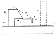
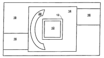
図1は、放出された光が白色光であるように燐光体12で被覆されたLEDダイ10の断面図である。図2は、図1の構造体の上面図である。
FIG. 1 is a cross-sectional view of an
LEDダイ10がサブマウント14上に装着される。サブマウント14は、金属接触パッドと、従来のメッキ又はリソグラフィ処理を用いてそこに形成されたリードとを有するシリコンスラブとすることができる。LEDダイ10の底にあるN及びP金属接点(フリップチップの例に対して)は、サブマウント14の上部の対応する金属パッドに接合される(例えば、半田付けされる)。上部の複数の金属パッドは、サブマウント14を通る複数のビア(via)によってサブマウント14の底の複数の金属パッドと電気的に結合される。このような構造は、当業技術で公知である。代替的に、サブマウント14に対する全ての電気接触を、サブマウント14の上部から行うこともできる。
The LED die 10 is mounted on the
サブマウント14の下部の金属パッドは、電源又は他のLEDに結合された金属リード16に接合される。リード16は、回路基板18又は他の支持構造体上のトレースとすることができる。回路基板18は、LEDダイ10からの熱を伝導して逃がすために絶縁アルミニウム基板を含むことができる。LEDダイのアレイを基板18上に装着して望ましい光出力をもたらすことができる。複数のLEDダイを単一サブマウント14上に装着することができ、これによってLEDダイを直列及び/又は並列に相互接続することができる。
The metal pad at the bottom of the
任意の形状のビームシャッタ20が、任意の適切な接着剤により又は他の任意の手段によりサブマウント14に固定される。一実施形態では、ビームシャッタ20は、サブマウント14上の金属パッドに半田付け、ろう付け、又は超音波溶接される。別の実施形態では、ビームシャッタ20は、エポキシを使用してサブマウント14に接着される。ビームシャッタ20は、アルミニウム又は他の任意の材料で形成することができる。
A
図1は、放出されたビーム21を垂直線から角度αのずれに限定するビームシャッタ20を示している。シャッタ20によって遮断されないLED光放射は、妨害を受けず、それによって光パターンが非対称性になることになる。各LEDダイに対してビームシャッタ20を使用するLEDアレイが自動車前照灯として使用されたとすれば、光は、前方と下方に向けられ、あらゆる上向きの光はビームシャッタによって制限されるであろう。
FIG. 1 shows a
ビームシャッタの高さ、形状、角度、及び位置が放出パターンを決める。高さは、望ましいパターンにより、LEDダイよりも若干厚いもの(例えば、1/10mm)から数ミリメートルまでの範囲とすることができる。シャッタは、光パターンに対する最良の制御が得られるようにLEDダイ又はサブマウントの近傍とすべきである。シャッタの角度は、ある一定の方向に光を反射させるために、放出された光に対して垂直以外の角度とすることができる。シャッタの典型的な幅は、1〜15mmである。シャッタの典型的な高さは、0.1〜10mmである。また、シャッタのダイ(又は、LEDレンズ)からの典型的距離は、0〜5mmである。 The height, shape, angle and position of the beam shutter determine the emission pattern. The height can range from slightly thicker than the LED die (eg, 1/10 mm) to several millimeters depending on the desired pattern. The shutter should be in the vicinity of the LED die or submount so that the best control over the light pattern is obtained. The angle of the shutter can be other than perpendicular to the emitted light in order to reflect the light in a certain direction. The typical width of the shutter is 1-15 mm. The typical height of the shutter is 0.1-10 mm. The typical distance from the shutter die (or LED lens) is 0-5 mm.
図3は、サブマウント14に固定された別の形状のビームシャッタ22の断面図である。ビームシャッタ22は、傾斜縁部を有する。このような傾斜した縁部は、光パターンをはっきりと定めるものである。
FIG. 3 is a cross-sectional view of another shape of the
図4は、回路基板18又はいずれかの他の支持構造体に固定された別の形状のビームシャッタ24の断面図である。ビームシャッタ24は、半田付け、ろう付け、超音波溶接、エポキシ、又は他の任意の適切な手段を用いて固定することができる。図4は、放出パターンを更に形成するための第2のビームシャッタ26の使用を点線の外形で示している。
FIG. 4 is a cross-sectional view of another shaped
図5は、湾曲したビームシャッタ28を有する、図2と類似の構造体の上面図である。湾曲は、より多くの光を捕らえるように作用することができ、又は放物レンズのように光を集光するように作用することができる。湾曲は、光を横向きパターンで反射させるために逆方向にさえすることができる。
FIG. 5 is a top view of a structure similar to FIG. 2 having a
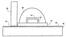
図6は、LEDダイが、その上に形成されるか又はそれに固定されたレンズ30を有することができる方法を示している。ビームシャッタ32は、レンズ30の内側又は外側とすることができる。レンズ30は、更に、放出された光を成形するものである。レンズ30は、コリメータレンズ、側面放射レンズ、又は他の任意の設計形状とすることができる。LED光を白色光(又は、いずれかの他の色の光)に変換するための燐光材料は、レンズ30の上に堆積させることができ、又は、レンズを形成する前に液体レンズ材料に燐光体粉末を混ぜるなどによってレンズ材料自体の一部を形成することができる。このような燐光体は公知である。
FIG. 6 illustrates how an LED die can have a
図7は、LEDダイ10のアレイ34をダイの関連ビームシャッタ20と共に示している。アレイは、アルミニウム基板を用いて回路基板上に装着することができる。このようなアレイは、ビームシャッタ20が光の上向きの放出を制限する自動車前照灯に有用であると考えられる。アレイは、従来の前照灯と同様に、単一レンズを有するカップ状ミラーに収納することができる。別の実施形態では、単一のビームシャッタは、複数のLEDダイから放出された光を選択的に遮断することができる。ビームシャッタはまた、レンズを有するLEDダイと共に使用することができる。
FIG. 7 shows an
本発明の特定的な実施形態を示して説明したが、本発明から逸脱することなくそのより広い態様における変更及び修正を行うことができ、従って、特許請求の範囲は、本発明の真の精神及び範囲に該当する時にこのような全ての変更及び修正をその範囲に包含するものであることが当業者には明らかであろう。 While particular embodiments of the present invention have been shown and described, changes and modifications can be made in its broader aspects without departing from the invention, and thus the claims are intended to be the true spirit of the invention. It will be apparent to those skilled in the art that all such changes and modifications are intended to be included in the scope when it falls within the scope.
10 LEDダイ
12 燐光体
14 サブマウント
18 回路基板
20 ビームシャッタ
10 LED die 12
Claims (26)
前記LEDダイを支持する装着面と、
光放出パターンを成形するために前記LEDダイの近くの前記装着面に固定された不透光ビームシャッタと、
を含むことを特徴とする発光装置。 A light emitting diode (LED) die;
A mounting surface for supporting the LED die;
An opaque beam shutter secured to the mounting surface near the LED die to shape a light emitting pattern;
A light emitting device comprising:
前記レンズからの前記ビームシャッタの距離は、0〜5mmである、
請求項1に記載の装置。 Further comprising a lens on the LED die;
The distance of the beam shutter from the lens is 0 to 5 mm.
The apparatus of claim 1.
発光ダイオード(LED)ダイを装着面上に設ける段階と、
前記LEDダイの近くの前記装着面に固定された不透光ビームシャッタを設ける段階と、
光放出パターンを成形するために放出される光の一部分が前記ビームシャッタによって遮断されるように、前記LEDダイを活性化して光を放出させる段階と、
を含むことを特徴とする方法。 A method for generating a light pattern comprising:
Providing a light emitting diode (LED) die on the mounting surface;
Providing an opaque light beam shutter secured to the mounting surface near the LED die;
Activating the LED die to emit light such that a portion of the light emitted to shape the light emission pattern is blocked by the beam shutter;
A method comprising the steps of:
前記レンズからの前記ビームシャッタの距離は、0〜5mmである、
請求項21に記載の方法。 A lens is on the LED die;
The distance of the beam shutter from the lens is 0 to 5 mm.
The method of claim 21.
Applications Claiming Priority (1)
| Application Number | Priority Date | Filing Date | Title |
|---|---|---|---|
| US11/053,091 US7316488B2 (en) | 2005-02-07 | 2005-02-07 | Beam shutter in LED package |
Publications (2)
| Publication Number | Publication Date |
|---|---|
| JP2006222430A true JP2006222430A (en) | 2006-08-24 |
| JP2006222430A5 JP2006222430A5 (en) | 2008-05-01 |
Family
ID=36499524
Family Applications (1)
| Application Number | Title | Priority Date | Filing Date |
|---|---|---|---|
| JP2006030175A Pending JP2006222430A (en) | 2005-02-07 | 2006-02-07 | Beam shutter in led package |
Country Status (4)
| Country | Link |
|---|---|
| US (1) | US7316488B2 (en) |
| JP (1) | JP2006222430A (en) |
| TW (1) | TW200711169A (en) |
| WO (1) | WO2006082559A1 (en) |
Cited By (3)
| Publication number | Priority date | Publication date | Assignee | Title |
|---|---|---|---|---|
| JP2008282575A (en) * | 2007-05-08 | 2008-11-20 | Stanley Electric Co Ltd | Led lamp for head lamp light source |
| US8070339B2 (en) | 2008-02-22 | 2011-12-06 | Stanley Electric Co., Ltd. | Vehicle lamp |
| US9207381B2 (en) | 2011-06-14 | 2015-12-08 | Sharp Kabushiki Kaisha | Backlight unit and liquid crystal display apparatus |
Families Citing this family (23)
| Publication number | Priority date | Publication date | Assignee | Title |
|---|---|---|---|---|
| US9212812B2 (en) | 2013-02-11 | 2015-12-15 | Cree, Inc. | LED light fixture with integrated light shielding |
| US20090086491A1 (en) | 2007-09-28 | 2009-04-02 | Ruud Lighting, Inc. | Aerodynamic LED Floodlight Fixture |
| US9028087B2 (en) | 2006-09-30 | 2015-05-12 | Cree, Inc. | LED light fixture |
| US7686469B2 (en) | 2006-09-30 | 2010-03-30 | Ruud Lighting, Inc. | LED lighting fixture |
| US9222632B2 (en) | 2013-01-31 | 2015-12-29 | Cree, Inc. | LED lighting fixture |
| US8092042B2 (en) * | 2007-05-03 | 2012-01-10 | Ruud Lighting, Inc. | Shield member in LED apparatus |
| US7637630B2 (en) * | 2008-04-22 | 2009-12-29 | Ruud Lighting, Inc. | Integrated shield-gasket member in LED apparatus |
| US7891835B2 (en) * | 2008-07-15 | 2011-02-22 | Ruud Lighting, Inc. | Light-directing apparatus with protected reflector-shield and lighting fixture utilizing same |
| US7918592B2 (en) * | 2008-07-25 | 2011-04-05 | Honeywell International Inc. | Integrated position light overlap baffles |
| DE102008048846A1 (en) * | 2008-09-25 | 2010-04-08 | Osram Opto Semiconductors Gmbh | Optoelectronic component |
| WO2010151600A1 (en) | 2009-06-27 | 2010-12-29 | Michael Tischler | High efficiency leds and led lamps |
| DE102009037559A1 (en) * | 2009-08-13 | 2011-02-17 | Automotive Lighting Reutlingen Gmbh | Headlamp with a LED-Teilfernlichtmodul |
| JP5506313B2 (en) * | 2009-09-30 | 2014-05-28 | スタンレー電気株式会社 | Light emitting diode light source for vehicle headlight |
| US8653539B2 (en) | 2010-01-04 | 2014-02-18 | Cooledge Lighting, Inc. | Failure mitigation in arrays of light-emitting devices |
| US9480133B2 (en) | 2010-01-04 | 2016-10-25 | Cooledge Lighting Inc. | Light-emitting element repair in array-based lighting devices |
| JP5518533B2 (en) * | 2010-03-12 | 2014-06-11 | 株式会社小糸製作所 | Vehicle headlamp and light emitting module for vehicle headlamp |
| CN102959708B (en) | 2010-06-29 | 2016-05-04 | 柯立芝照明有限公司 | There is the electronic installation of flexible substrate |
| KR101830717B1 (en) * | 2011-06-30 | 2018-02-21 | 엘지이노텍 주식회사 | A light emitting device pakage |
| US9231178B2 (en) | 2012-06-07 | 2016-01-05 | Cooledge Lighting, Inc. | Wafer-level flip chip device packages and related methods |
| US9435519B2 (en) | 2013-01-31 | 2016-09-06 | Cree, Inc. | Light-fixture support assembly |
| KR101665760B1 (en) * | 2014-05-12 | 2016-10-24 | 엘지전자 주식회사 | Light emitting module and lighting apparatus having the same |
| US10578267B2 (en) * | 2016-10-26 | 2020-03-03 | North American Lighting, Inc. | Vehicle lamp light assembly |
| CN217131136U (en) * | 2021-09-23 | 2022-08-05 | 法雷奥照明湖北技术中心有限公司 | Lighting device and motor vehicle |
Family Cites Families (14)
| Publication number | Priority date | Publication date | Assignee | Title |
|---|---|---|---|---|
| JP3232389B2 (en) * | 1994-12-30 | 2001-11-26 | タキロン株式会社 | Dot matrix light emitting display with shading louver |
| JPH10233534A (en) * | 1997-02-21 | 1998-09-02 | Nichia Chem Ind Ltd | Led display and display device using it |
| JPH10268800A (en) * | 1997-03-21 | 1998-10-09 | Sony Corp | Display device |
| JP2000183407A (en) * | 1998-12-16 | 2000-06-30 | Rohm Co Ltd | Optical semiconductor device |
| JP3619719B2 (en) * | 1999-08-31 | 2005-02-16 | 三洋電機株式会社 | Display part of electrical equipment |
| KR100832956B1 (en) * | 2000-04-24 | 2008-05-27 | 로무 가부시키가이샤 | Edge-emitting light-emitting semiconductor device |
| DE10033502A1 (en) * | 2000-07-10 | 2002-01-31 | Osram Opto Semiconductors Gmbh | Optoelectronic module, process for its production and its use |
| DE10044455B4 (en) * | 2000-09-08 | 2009-07-30 | Osram Opto Semiconductors Gmbh | signal light |
| AT5495U1 (en) * | 2001-04-09 | 2002-07-25 | Bartenbach Christian | LUMINAIRE FOR LIGHTING ROOMS WITH A VARIETY OF LEDS |
| US20040032728A1 (en) * | 2002-08-19 | 2004-02-19 | Robert Galli | Optical assembly for LED chip package |
| US6945672B2 (en) * | 2002-08-30 | 2005-09-20 | Gelcore Llc | LED planar light source and low-profile headlight constructed therewith |
| JP4294295B2 (en) * | 2002-11-06 | 2009-07-08 | 株式会社小糸製作所 | Vehicle headlamp |
| JP4040955B2 (en) * | 2002-11-06 | 2008-01-30 | 株式会社小糸製作所 | Vehicle headlamp and manufacturing method thereof |
| US7005679B2 (en) * | 2003-05-01 | 2006-02-28 | Cree, Inc. | Multiple component solid state white light |
-
2005
- 2005-02-07 US US11/053,091 patent/US7316488B2/en not_active Expired - Fee Related
-
2006
- 2006-02-01 WO PCT/IB2006/050339 patent/WO2006082559A1/en not_active Application Discontinuation
- 2006-02-03 TW TW095103823A patent/TW200711169A/en unknown
- 2006-02-07 JP JP2006030175A patent/JP2006222430A/en active Pending
Cited By (3)
| Publication number | Priority date | Publication date | Assignee | Title |
|---|---|---|---|---|
| JP2008282575A (en) * | 2007-05-08 | 2008-11-20 | Stanley Electric Co Ltd | Led lamp for head lamp light source |
| US8070339B2 (en) | 2008-02-22 | 2011-12-06 | Stanley Electric Co., Ltd. | Vehicle lamp |
| US9207381B2 (en) | 2011-06-14 | 2015-12-08 | Sharp Kabushiki Kaisha | Backlight unit and liquid crystal display apparatus |
Also Published As
| Publication number | Publication date |
|---|---|
| US20060175626A1 (en) | 2006-08-10 |
| US7316488B2 (en) | 2008-01-08 |
| TW200711169A (en) | 2007-03-16 |
| WO2006082559A1 (en) | 2006-08-10 |
Similar Documents
| Publication | Publication Date | Title |
|---|---|---|
| JP2006222430A (en) | Beam shutter in led package | |
| TWI400819B (en) | Light emitting diode module for line light source | |
| JP4143732B2 (en) | In-vehicle wavelength converter | |
| US6940704B2 (en) | Semiconductor light emitting device | |
| KR101266205B1 (en) | Light emitting device and method for manufacturing the same | |
| US7422349B2 (en) | Led lighting apparatus | |
| JP4771179B2 (en) | Lighting device | |
| CN109964323A (en) | Light emitting device package and light source equipment including the light emitting device package | |
| TW200915616A (en) | Semiconductor light-emitting device | |
| JP2005093728A (en) | Light-emitting device | |
| JP2007035802A (en) | Light-emitting device | |
| JP2006245032A (en) | Light emitting device and led lamp | |
| JP2006049442A (en) | Semiconductor light emission device and its manufacturing method | |
| JP2012533902A (en) | Light emitting diode with molded reflective sidewall coating | |
| US20120299463A1 (en) | Light emitting device and illumination apparatus using same | |
| JP2006185967A (en) | Light emitting device storage package, light emitting device and lighting device | |
| US20190341536A1 (en) | Semiconductor device and semiconductor device package | |
| TW201909451A (en) | Light emitting device package | |
| JP2008258567A (en) | Light emitting device and method of manufacturing the same | |
| TWI775911B (en) | Light emitting device package | |
| JP4442536B2 (en) | LED lighting device | |
| JP5605626B2 (en) | Vehicle lighting | |
| JP4820133B2 (en) | Light emitting device | |
| JP3941826B2 (en) | LED luminaire manufacturing method | |
| US7001824B2 (en) | Gallium nitride vertical light emitting diode structure and method of separating a substrate and a thin film in the structure |
Legal Events
| Date | Code | Title | Description |
|---|---|---|---|
| A521 | Written amendment |
Free format text: JAPANESE INTERMEDIATE CODE: A523 Effective date: 20080313 |
|
| A621 | Written request for application examination |
Free format text: JAPANESE INTERMEDIATE CODE: A621 Effective date: 20080313 |
|
| A131 | Notification of reasons for refusal |
Free format text: JAPANESE INTERMEDIATE CODE: A131 Effective date: 20091005 |
|
| A02 | Decision of refusal |
Free format text: JAPANESE INTERMEDIATE CODE: A02 Effective date: 20100308 |