JP2006174463A - Impedance and/or polarization matched planar antenna - Google Patents
Impedance and/or polarization matched planar antenna Download PDFInfo
- Publication number
- JP2006174463A JP2006174463A JP2005359280A JP2005359280A JP2006174463A JP 2006174463 A JP2006174463 A JP 2006174463A JP 2005359280 A JP2005359280 A JP 2005359280A JP 2005359280 A JP2005359280 A JP 2005359280A JP 2006174463 A JP2006174463 A JP 2006174463A
- Authority
- JP
- Japan
- Prior art keywords
- slot
- antenna
- impedance
- planar antenna
- polarization
- Prior art date
- Legal status (The legal status is an assumption and is not a legal conclusion. Google has not performed a legal analysis and makes no representation as to the accuracy of the status listed.)
- Pending
Links
Images


Classifications
-
- H—ELECTRICITY
- H01—ELECTRIC ELEMENTS
- H01Q—ANTENNAS, i.e. RADIO AERIALS
- H01Q13/00—Waveguide horns or mouths; Slot antennas; Leaky-waveguide antennas; Equivalent structures causing radiation along the transmission path of a guided wave
- H01Q13/10—Resonant slot antennas
- H01Q13/106—Microstrip slot antennas
-
- H—ELECTRICITY
- H01—ELECTRIC ELEMENTS
- H01Q—ANTENNAS, i.e. RADIO AERIALS
- H01Q13/00—Waveguide horns or mouths; Slot antennas; Leaky-waveguide antennas; Equivalent structures causing radiation along the transmission path of a guided wave
- H01Q13/10—Resonant slot antennas
-
- H—ELECTRICITY
- H01—ELECTRIC ELEMENTS
- H01Q—ANTENNAS, i.e. RADIO AERIALS
- H01Q25/00—Antennas or antenna systems providing at least two radiating patterns
-
- H—ELECTRICITY
- H01—ELECTRIC ELEMENTS
- H01Q—ANTENNAS, i.e. RADIO AERIALS
- H01Q3/00—Arrangements for changing or varying the orientation or the shape of the directional pattern of the waves radiated from an antenna or antenna system
- H01Q3/24—Arrangements for changing or varying the orientation or the shape of the directional pattern of the waves radiated from an antenna or antenna system varying the orientation by switching energy from one active radiating element to another, e.g. for beam switching
Landscapes
- Waveguide Aerials (AREA)
- Variable-Direction Aerials And Aerial Arrays (AREA)
Abstract
Description
本発明は、与えられた周波数で動作するよう大きさを決められた閉曲線型スロットを有する、基板上に設けられたプレーナ型アンテナに関する。その周波数は、給電点として知られる点で該スロットと交差する給電線により供給される。 The present invention relates to a planar antenna mounted on a substrate having a closed curved slot sized to operate at a given frequency. The frequency is supplied by a feed line that intersects the slot at what is known as a feed point.
上記アンテナはローカルワイヤレスネットワークに好適である。従来、(例えば環状)スロットは、KNORRディメンションルールによるマイクロストリップラインへの電磁気的結合により給電される。 The antenna is suitable for a local wireless network. Traditionally (eg, annular) slots are powered by electromagnetic coupling to the microstrip line according to the KNORR dimension rule.
上記のように給電されるので、給電点に対応する電気平面内のインピーダンスは、基板及びスロットのパラメータに応じて、300オームないし400オームの間にある。よって、このタイプの供給には、50オームまたはより一般的なインピーダンス値における適応のためにインピーダンスを下げるため、インピーダンス変換器が必要である。このインピーダンス変換(例えば4分の1波長ベース)は、煩わしく、ライン損失を生じ、帯域幅を狭めてしまう。 Since power is fed as described above, the impedance in the electrical plane corresponding to the feed point is between 300 ohms and 400 ohms, depending on the substrate and slot parameters. Thus, this type of supply requires an impedance converter to lower the impedance for adaptation at 50 ohms or more general impedance values. This impedance conversion (for example, quarter-wave base) is cumbersome and causes line loss and narrows the bandwidth.
さらに、このタイプの給電によると、分極は線形であり、その方向は給電点により決まる。分極方向を修正するには給電点を変える必要がある。 Furthermore, with this type of feed, the polarization is linear and the direction is determined by the feed point. To correct the polarization direction, it is necessary to change the feeding point.
本発明は、給電点におけるインピーダンスを変更でき、分極方向を修正できるプレーナ型アンテナを提案するものである。 The present invention proposes a planar antenna that can change the impedance at the feeding point and can correct the polarization direction.
本発明は、給電点におけるインピーダンス及び/またはアンテナの分極がマッチするように、スロット上に並列に少なくとも2つの短絡回路を給電点に対して配置したアンテナに関する。 The present invention relates to an antenna in which at least two short circuits are arranged in parallel on a slot with respect to a feeding point so that impedance at the feeding point and / or polarization of the antenna match.
本発明によると、留意すべきことは、給電線、及びスロット上に配置された2つの短絡回路の相対的位置を選択することにより、スロットの給電点におけるインピーダンスを修正し、アンテナの分極方向を修正することができることである。 According to the present invention, it should be noted that the impedance at the feed point of the slot is modified by selecting the feed line and the relative position of the two short circuits placed on the slot, and the polarization direction of the antenna is changed. It can be corrected.
第1の実施形態において、前記短絡回路は固定され、前記給電点の位置を修正して前記給電点への前記インピーダンスを修正する。 In the first embodiment, the short circuit is fixed and the position of the feeding point is corrected to correct the impedance to the feeding point.
実際、留意すべきことは、給電点の位置を変えることにより、給電点のインピーダンスを修正することができることである。短絡回路が固定されている場合、インピーダンスの修正によりアンテナの分極が変わらないことにも留意すべきである。実際、分極を決めるのは短絡回路である。 In fact, it should be noted that the impedance of the feed point can be modified by changing the position of the feed point. It should also be noted that when the short circuit is fixed, the antenna polarization does not change due to the impedance modification. In fact, it is the short circuit that determines the polarization.
第2の実施形態において、給電点を固定し、短絡回路の位置を変えて分極を修正する。 In the second embodiment, the feeding point is fixed and the position of the short circuit is changed to correct the polarization.
この場合、アンテナの分極を修正することができる。しかし、留意すべきことは、これにより一般的には給電点におけるインピーダンスが変化する。 In this case, the polarization of the antenna can be corrected. However, it should be noted that this generally changes the impedance at the feed point.
具体的実施形態において、前記スロットはそれが含まれる平面と垂直な対称軸を有し、前記スロット上に互いに90°の角度で配置された4つの短絡回路が正反対の短絡回路のペアごとにアクティブとされ、2つの分極を有するアンテナとなる。 In a specific embodiment, the slot has an axis of symmetry perpendicular to the plane in which it is contained, and four short circuits arranged at 90 ° angles to each other on the slot are active for each pair of diametrically opposed short circuits. Thus, the antenna has two polarizations.
有利にも、前記給電線は前記短絡回路のひとつから45°の角度に配置される。 Advantageously, the feed line is arranged at a 45 ° angle from one of the short circuits.
実際、この場合、両方の分極に対してインピーダンスは同じであり、インピーダンス変換器を付加する必要はない。 In fact, in this case, the impedance is the same for both polarizations and there is no need to add an impedance converter.
一実施形態において、前記スロットはそれが含まれる平面と垂直な対称軸を有し、前記2つの短絡回路は前記スロット上でこの軸に対して幾何学的に反対にあり、短絡回路平面を形成している。 In one embodiment, the slot has an axis of symmetry perpendicular to the plane in which it is contained, and the two short circuits are geometrically opposite to the axis on the slot to form a short circuit plane is doing.
本発明によると、前記スロットは環状、正方形、長方形、または多角形であり、前記短絡回路は、ダイオード等のスイッチングデバイスを用いて作ることができる。 According to the present invention, the slot is circular, square, rectangular, or polygonal, and the short circuit can be made using a switching device such as a diode.
本発明は、プレーナ型アンテナの製造方法にも関する。該方法は、前記スロット(F)上に平行に少なくとも2つの短絡回路(SC)を配置するステップを含み、前記短絡回路の前記給電点(E)に対する位置は、前記給電点(E)へのインピーダンス及び/または前記アンテナの分極をマッチするように選択される。 The present invention also relates to a method for manufacturing a planar antenna. The method includes disposing at least two short circuits (SC) in parallel on the slot (F), and the position of the short circuit with respect to the feeding point (E) is relative to the feeding point (E). It is selected to match the impedance and / or polarization of the antenna.
本発明のその他の特徴と利点は、添付した図面を参照して異なる実施形態の説明を読めば明らかとなるであろう。 Other features and advantages of the present invention will become apparent from the description of different embodiments with reference to the accompanying drawings.
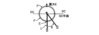
図1は、本発明によるアンテナを示す図である。このアンテナは、紙面に対応する基板上に配置されている。このアンテナは、閉曲線形(ここでは、環状)のスロットFを有する。このアンテナは、与えられた周波数で動作するように大きさが決められており、給電点EでスロットFを横切る給電線Lにより給電されている。より具体的には、環状スロットの周は、λsに等しい。ここで、λsはスロット中の導波波長である。本発明によると、スロットは環状スロットF上に平行に正反対に配置された2つの短絡回路SCを有する。給電点におけるインピーダンスを修正するように、給電点に対して配置されている。この修正について以下説明する。 FIG. 1 shows an antenna according to the present invention. This antenna is disposed on a substrate corresponding to the paper surface. This antenna has a slot F having a closed curve shape (here, annular). This antenna is sized to operate at a given frequency and is fed by a feed line L that traverses the slot F at a feed point E. More specifically, the circumference of the annular slot is equal to λs. Here, λs is the waveguide wavelength in the slot. According to the invention, the slot has two short-circuit circuits SC arranged on the annular slot F in parallel and oppositely. It arrange | positions with respect to a feed point so that the impedance in a feed point may be corrected. This correction will be described below.
ラインが短絡回路により決まる平面と垂直な時、上記のアンテナではカップリン状態が最適になることが知られている。この場合、物理的短絡回路はラインにより有機された短絡回路と一致するからである。図1において、両方の短絡回路に対して給電線を角θだけ動かすことにより給電点を変位させたとき、給電点におけるインピーダンスが変化する。 It is known that the coupling state is optimal for the above antenna when the line is perpendicular to the plane determined by the short circuit. In this case, the physical short circuit coincides with the short circuit organized by the line. In FIG. 1, when the feed point is displaced by moving the feed line by an angle θ with respect to both short-circuits, the impedance at the feed point changes.
給電線は、例えば、単にスロットFの半周の一方に配置された複数の給電線によって移動され、必要に応じてインピーダンスを修正する必要がある場合に活性化される。 For example, the feeder is simply moved by a plurality of feeders arranged on one half of the slot F, and activated when the impedance needs to be corrected as necessary.
必要なインピーダンスは決まっており、必要なインピーダンスによる角θを有する単一のラインを配置する場合にも本発明を適用することができる。 The necessary impedance is determined, and the present invention can be applied to a case where a single line having an angle θ depending on the necessary impedance is arranged.
本発明によると、スロットとライン間の結合状態は最適状態と比して劣っている。しかし、給電点がスロットの短絡回路点上にない限り、結合方程式C=E∧Hはヌルではない。実際、電場EはスロットFの構成により決まり、磁場HはラインLの構成により決まる。ラインLを角θ動かすことにより、値Cは減少するが相殺されることはなく、インピーダンスをマッチさせることができる。給電点の位置により、給電された半リング上でインピーダンスを変化させることが可能である。このインピーダンスは、結合状態が最大になったとき、すなわちラインを半リングの中央にした時に、最大値となる。 According to the present invention, the coupling state between the slot and the line is inferior to the optimum state. However, the coupling equation C = E∧H is not null unless the feed point is on the short circuit point of the slot. Actually, the electric field E is determined by the configuration of the slot F, and the magnetic field H is determined by the configuration of the line L. By moving the line L by the angle θ, the value C decreases but is not canceled out, and the impedance can be matched. Depending on the position of the feeding point, it is possible to change the impedance on the fed half ring. This impedance is maximum when the coupling state is maximized, that is, when the line is centered in the half ring.
短絡回路により、半リング中の場の分布は決まる。 The short circuit determines the field distribution in the half ring.
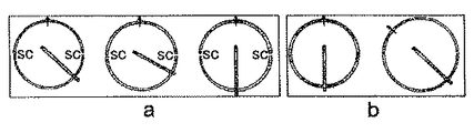
図2は、本発明(図2a)及び従来技術(図2b)によるプレーナ型アンテナのいろいろな実施形態のスロット中の電流分布とその結果生じる分極を示す図である。留意すべきことは、図2aにおいて、分極は給電点の位置を変えても変わらないが、図2bに示したように、スロットが短絡回路を有さない時は、分極が給電線とともに回転してしまうことである。 FIG. 2 shows the current distribution in the slot and the resulting polarization of various embodiments of the planar antenna according to the invention (FIG. 2a) and the prior art (FIG. 2b). It should be noted that in FIG. 2a, the polarization does not change even if the position of the feed point is changed, but as shown in FIG. 2b, when the slot does not have a short circuit, the polarization rotates with the feed line. It is to end up.
よって、スロット上に少なくとも2つの短絡回路を使用することにより、スロットにより分極が決まるようになる。実際、短絡回路を有しない、または単一の短絡回路のみを有する標準的なスロットの場合とは逆に、線形分極の方向は給電点の位置によって回らなく、短絡回路によって決まる。それゆえ、分極は、給電点がどこにあろうが、短絡回路の平面に対して垂直である。 Thus, by using at least two short circuits on the slot, the polarization is determined by the slot. In fact, contrary to the case of a standard slot with no short circuit or only a single short circuit, the direction of linear polarization does not depend on the position of the feed point, but depends on the short circuit. Therefore, the polarization is perpendicular to the plane of the short circuit wherever the feed point is.
図3は、図1に示した実現主義の原則による、アンテナの給電点の5通りの位置を示す図である。これらのアンテナにおいて、2つの正反対の短絡回路が環状スロット上に構成されている。このように、2つの長さLs/2の半リングが互いに向き合っている。 FIG. 3 is a diagram showing five positions of the feeding point of the antenna based on the principle of realization shown in FIG. In these antennas, two diametrically opposed short circuits are configured on the annular slot. In this way, the two half rings of length Ls / 2 face each other.
実際、これらのアンテナは、Rogers4003(Er=3.38、h=0.81mm)の絶縁基板上で、5.8GHzで動作するように大きさを決めてシミュレーションした。環状スロットの周はスロット(Ls)、すなわち半径6.65mm中を導かれた波長のオーダーでなければならない。 In fact, these antennas were sized and simulated to operate at 5.8 GHz on a Rogers4003 (Er = 3.38, h = 0.81 mm) insulating substrate. The circumference of the annular slot must be of the order of the wavelength guided in the slot (Ls), ie a radius of 6.65 mm.
図4に、異なるアンテナのインピーダンスを示した。インピーダンスの値は、例えば、短絡回路から90°のライン位置に対する350オームから、60°のライン位置に対する70オーム未満の値までの範囲にある。これらの結果により、本発明がアンテナのインピーダンスをマッチできることが確認でき、インピーダンスマッチングの可能な拡張を示している。 FIG. 4 shows the impedance of different antennas. Impedance values range, for example, from 350 ohms for a 90 ° line position to a value less than 70 ohms for a 60 ° line position from the short circuit. From these results, it can be confirmed that the present invention can match the impedance of the antenna, and indicates an extension of possible impedance matching.
図5は、図3の実施形態において、短絡回路平面及びそれに垂直な平面によりそれぞれ決まる、平面H及びVの電場Eの4つの成分を示す図である。留意すべきことは、給電点の位置にかかわらず、主成分は無指向性(3dBのオーダーの指向性)であり、crosspolarizationレベルはcopolarizationレベルより非常に低い(少なくとも10dB)ことである。これらの数字により、標準的な最大結合位置からシフトしている時、リニア分極が保存されることが確認できる。 FIG. 5 is a diagram showing the four components of the electric field E in the planes H and V respectively determined by the short circuit plane and the plane perpendicular thereto in the embodiment of FIG. It should be noted that regardless of the position of the feed point, the main component is omnidirectional (directivity on the order of 3 dB) and the crosspolarization level is much lower (at least 10 dB) than the copolarization level. These numbers confirm that linear polarization is preserved when shifting from the standard maximum binding position.
より具体的な実施形態を検討した。図6に示した実施形態において、アンテナ2は2つの正反対の短絡回路と、基準点から51°の角度にある給電点とを有する。インピーダンスは約50オームであり、直接このインピーダンス値とマッチさせることができる。これは、図6に示した標準的アンテナ1の場合のように、スロットの外側からラインを長く延長する必要がないことを意味する。よって、留意すべきことは、標準アンテナ1の場合、ラインが短絡回路平面に対して90°をなす時、上記インピーダンスを得るために必要なグランド平面(斜線部)のサイズは30×35mm2であり、一方、本発明の場合、ラインを長くすること以外の手段でインピーダンスマッチングを実現しているので、必要なサイズは30×27mm2だけであることである。このように、本発明により、コンパクト性を担保することができる。
More specific embodiments were considered. In the embodiment shown in FIG. 6, the
図6は、-10dBにおける帯域幅がより広いことを示している。アンテナ2の場合帯域幅は23.1%であり、標準アンテナ1の場合、帯域幅は7%である。
FIG. 6 shows that the bandwidth at -10 dB is wider. In the case of
図7は、放射パターンを示し、給電点が動いても、放射パターンは少ししか変わらないことを示している。 FIG. 7 shows the radiation pattern, which shows that the radiation pattern changes only slightly when the feed point moves.
図8は、本発明によるプレーナ型アンテナを示す図であり、給電点Eは固定されているが、短絡回路位置SC1とSC2が変わっている。この場合、短絡回路平面とともに分極も回転している。 FIG. 8 is a diagram showing a planar antenna according to the present invention. The feeding point E is fixed, but the short circuit positions SC1 and SC2 are changed. In this case, the polarization also rotates with the short circuit plane.
短絡回路は、例えばダイオードを用いて実施する。ダイオードは正反対のペアとして有利に動作する。 The short circuit is implemented using a diode, for example. The diodes advantageously operate as diametrically opposite pairs.
図9は、本発明の原理により得られた分極の多様性を示す、プレーナ型アンテナの一実施形態を示す図である。この実施形態において、4つのダイオードが互いに角度90°でスロット上に配置されている。対向するダイオードを2つずつ切り替えることにより、単一の給電点を用いて、2つの線形分極状態にアクセスすることができる。給電点位置は、短絡回路平面の一方から45°のところに選択され、両方の分極状態で同じインピーダンスを有する。 FIG. 9 is a diagram illustrating one embodiment of a planar antenna showing the diversity of polarization obtained according to the principles of the present invention. In this embodiment, four diodes are arranged on the slot at an angle of 90 ° to each other. By switching between two opposing diodes, two linear polarization states can be accessed using a single feed point. The feed point position is selected 45 ° from one of the short circuit planes and has the same impedance in both polarization states.
第1の分極状態は、ダイオードD1とD3が非電導状態、ダイオードD2とD4が電導状態である第1の構成に対応する。分極は、図10aの放射パターンに示したように水平である。逆に、第2の分極状態は、ダイオードD1とD3が電導状態、ダイオードD2とD4が非電導状態である第2の構成に対応する。分極は、図10bの放射パターンに示したように垂直である。 The first polarization state corresponds to the first configuration in which the diodes D1 and D3 are in a non-conductive state and the diodes D2 and D4 are in a conductive state. The polarization is horizontal as shown in the radiation pattern of FIG. 10a. Conversely, the second polarization state corresponds to the second configuration in which the diodes D1 and D3 are in the conductive state and the diodes D2 and D4 are in the nonconductive state. The polarization is vertical as shown in the radiation pattern of FIG. 10b.
ここではダイオードのペアが2つある場合のみを説明したが、本発明によれば、nのオーダーの分極の多様性を有するアンテナが可能となる。ここで、nは、スロットにある短絡回路平面の数である。 Here, only the case where there are two pairs of diodes has been described, but according to the present invention, an antenna having a diversity of polarization on the order of n is possible. Here, n is the number of short circuit planes in the slot.
よって、本発明によれば、いかなるインピーダンスの場合でも、直接マッチングが可能なアンテナを得ることができる。これは、インピーダンス変換器が必要ないので、アンテナがよりコンパクトになり、帯域幅が広くなり、構造的にライン損失を減らすことができる。 Therefore, according to the present invention, it is possible to obtain an antenna that can be directly matched with any impedance. This eliminates the need for an impedance converter, thus making the antenna more compact, wider bandwidth, and structurally reducing line loss.
本発明により、分極ダイバーシティアンテナ構造を得ることができる。短絡回路位置を変更することにより、給電点を変更することなく、分極を変えるえることができる。 According to the present invention, a polarization diversity antenna structure can be obtained. By changing the position of the short circuit, the polarization can be changed without changing the feeding point.
本発明は、以上の実施形態に限定されない。当業者は、実施形態をいろいろ変形できることが分かるであろう。例えば、他の形(正方形、多角形等)の閉曲線スロットを使用することができる。いろいろなスロット給電方法(例えば、マイクロストリップ、トリプレート、コプラナー、同軸給電方式)を使用することができる。1つの状態から他の状態にスイッチにいろいろなアクティブエレメント(ダイオード、トランジスタ、MEM等)を使用することができる。スロットを基本モードまたは高次モードで使用することができる。複数の短絡回路を使用して、必ずしも正反対の短絡回路平面や短絡回路ペア平面等を決めるために配置しなくてもよい。 The present invention is not limited to the above embodiment. Those skilled in the art will appreciate that the embodiments can be varied in many ways. For example, closed curve slots of other shapes (squares, polygons, etc.) can be used. Various slot feeding methods (for example, microstrip, triplate, coplanar, coaxial feeding method) can be used. Various active elements (diodes, transistors, MEM, etc.) can be used in the switch from one state to another. Slots can be used in basic mode or higher order mode. It is not always necessary to use a plurality of short-circuits to determine the opposite short-circuit plane or the short-circuit pair plane.
E 給電点
F スロット
L 給電線
SC 短絡回路
D1、D2、D3、D4 ダイオード
E Feeding point
F slot
L Feed line
SC short circuit
D1, D2, D3, D4 diodes
Claims (11)
前記給電点へのインピーダンス及び/または前記アンテナの分極をマッチするように、少なくとも2つの短絡回路が前記スロット上に平行に前記給電点に対して配置されていることを特徴とするアンテナ。 A planar antenna on a substrate having a closed-curved slot sized to operate at one frequency and fed by a feed line that intersects the slot at a point known as a feed point. ,
An antenna, characterized in that at least two short circuits are arranged on the slot in parallel to the feed point so as to match the impedance to the feed point and / or the polarization of the antenna.
前記短絡回路は固定され、前記給電点の位置を修正して前記インピーダンスを修正したことを特徴とするアンテナ。 The planar antenna according to claim 1, wherein
The antenna is characterized in that the short circuit is fixed and the impedance is corrected by correcting the position of the feeding point.
前記給電点は固定され、前記短絡回路の位置を修正して前記分極を修正したことを特徴とするアンテナ。 The planar antenna according to claim 1, wherein
The antenna is characterized in that the feeding point is fixed and the polarization is corrected by correcting the position of the short circuit.
前記スロットはそれが含まれる平面と垂直な対称軸を有し、
前記スロット上に互いに90°の角度で配置された4つの短絡回路が正反対の短絡回路のペアごとにアクティブとされ、2つの分極を有するアンテナとなることを特徴とするアンテナ。 A planar antenna according to claim 3,
Said slot has an axis of symmetry perpendicular to the plane in which it is contained;
The antenna according to claim 1, wherein four short-circuits arranged at an angle of 90 ° to each other on the slot are made active for each pair of diametrically opposite short-circuits, and the antenna has two polarizations.
前記給電線は前記短絡回路のひとつから45°の角度に配置されたことを特徴とするアンテナ。 A planar antenna according to claim 4,
The antenna according to claim 1, wherein the feeder is disposed at an angle of 45 ° from one of the short circuits.
前記スロットはそれが含まれる平面と垂直な対称軸を有し、
前記2つの短絡回路は前記スロット上でこの軸に対して幾何学的に反対にあり、短絡回路平面を形成していることを特徴とするアンテナ。 A planar antenna according to any one of claims 1 to 3,
Said slot has an axis of symmetry perpendicular to the plane in which it is contained;
The antenna characterized in that the two short circuits are geometrically opposite to the axis on the slot and form a short circuit plane.
両方の短絡回路は、前記給電点に対して90°とは異なる角度で前記軸の回りに配置されていることを特徴とするアンテナ。 The planar antenna according to claim 6, wherein
Both antennas are arranged around the axis at an angle different from 90 ° with respect to the feed point.
前記スロットは環状、正方形、長方形、または多角形であることを特徴とするアンテナ。 A planar antenna according to any one of claims 1 to 7,
The antenna is characterized in that the slot is annular, square, rectangular, or polygonal.
前記短絡回路は、スイッチングデバイスを用いて実現されていることを特徴とするアンテナ。 A planar antenna according to any one of claims 1 to 8,
The short circuit is realized by using a switching device.
前記スイッチングデバイスはダイオードであることを特徴とするアンテナ。 The planar antenna according to claim 9, wherein
The antenna, wherein the switching device is a diode.
前記スロット上に平行に少なくとも2つの短絡回路を配置するステップを含み、
前記短絡回路の前記給電点に対する位置は、前記給電点へのインピーダンス及び/または前記アンテナの分極をマッチするように選択されることを特徴とする方法。 A method of manufacturing a planar antenna on a substrate having a closed-curved slot sized to operate at one frequency and fed by a feed line that intersects the slot at a point known as a feed point Because
Disposing at least two short circuits in parallel on said slot;
The position of the short circuit with respect to the feed point is selected to match the impedance to the feed point and / or the polarization of the antenna.
Applications Claiming Priority (1)
| Application Number | Priority Date | Filing Date | Title |
|---|---|---|---|
| FR0452948A FR2879355A1 (en) | 2004-12-13 | 2004-12-13 | Planar antenna for wireless local area network, has two short-circuits lying parallel to closed curve shaped slot and positioned with respect to excitation point so as to adapt impedance to excitation point and/or polarization of antenna |
Publications (2)
| Publication Number | Publication Date |
|---|---|
| JP2006174463A true JP2006174463A (en) | 2006-06-29 |
| JP2006174463A5 JP2006174463A5 (en) | 2009-01-29 |
Family
ID=34952399
Family Applications (1)
| Application Number | Title | Priority Date | Filing Date |
|---|---|---|---|
| JP2005359280A Pending JP2006174463A (en) | 2004-12-13 | 2005-12-13 | Impedance and/or polarization matched planar antenna |
Country Status (8)
| Country | Link |
|---|---|
| US (1) | US7420518B2 (en) |
| EP (1) | EP1684377A1 (en) |
| JP (1) | JP2006174463A (en) |
| KR (1) | KR101151916B1 (en) |
| CN (1) | CN1805211B (en) |
| BR (1) | BRPI0505393A (en) |
| FR (1) | FR2879355A1 (en) |
| MX (1) | MXPA05013516A (en) |
Cited By (1)
| Publication number | Priority date | Publication date | Assignee | Title |
|---|---|---|---|---|
| CN102771195A (en) * | 2010-02-24 | 2012-11-07 | 西门子公司 | DC high voltage source and particle accelerator |
Families Citing this family (1)
| Publication number | Priority date | Publication date | Assignee | Title |
|---|---|---|---|---|
| EP2514029A1 (en) | 2009-12-16 | 2012-10-24 | Adant SRL | Reconfigurable antenna system for radio frequency identification (rfid) |
Citations (3)
| Publication number | Priority date | Publication date | Assignee | Title |
|---|---|---|---|---|
| JPH05267923A (en) * | 1992-03-19 | 1993-10-15 | Kokusai Kagaku Shinko Zaidan | Slot antenna |
| JP2004304226A (en) * | 2003-03-28 | 2004-10-28 | Matsushita Electric Ind Co Ltd | Antenna device and radio communication apparatus using the same |
| JP2005217667A (en) * | 2004-01-28 | 2005-08-11 | Nippon Dempa Kogyo Co Ltd | Slot line type flat antenna |
Family Cites Families (6)
| Publication number | Priority date | Publication date | Assignee | Title |
|---|---|---|---|---|
| FR1129288A (en) * | 1955-07-28 | 1957-01-17 | Sadir Carpentier | Improvements to directive antennas |
| GB1546571A (en) * | 1976-07-30 | 1979-05-23 | Antenna Specialists Uk Ltd | Antenna |
| RU1775757C (en) * | 1991-03-29 | 1992-11-15 | Казанский Авиационный Институт Им.А.Н.Туполева | Polarization switch |
| FR2826512B1 (en) * | 2001-06-22 | 2003-08-29 | Thomson Licensing Sa | COMPACT ANTENNA WITH ANNULAR SLOT |
| FR2833764B1 (en) * | 2001-12-19 | 2004-01-30 | Thomson Licensing Sa | DEVICE FOR RECEIVING AND / OR TRANSMITTING CIRCULARLY POLARIZED ELECTROMAGNETIC SIGNALS |
| FR2840456A1 (en) * | 2002-05-31 | 2003-12-05 | Thomson Licensing Sa | IMPROVEMENT TO SLOT PLANAR ANTENNAS |
-
2004
- 2004-12-13 FR FR0452948A patent/FR2879355A1/en active Pending
-
2005
- 2005-11-21 EP EP20050111030 patent/EP1684377A1/en not_active Withdrawn
- 2005-11-28 US US11/287,999 patent/US7420518B2/en not_active Expired - Fee Related
- 2005-12-01 CN CN2005101272983A patent/CN1805211B/en not_active Expired - Fee Related
- 2005-12-06 BR BRPI0505393-5A patent/BRPI0505393A/en not_active IP Right Cessation
- 2005-12-07 KR KR1020050118744A patent/KR101151916B1/en not_active IP Right Cessation
- 2005-12-13 MX MXPA05013516A patent/MXPA05013516A/en active IP Right Grant
- 2005-12-13 JP JP2005359280A patent/JP2006174463A/en active Pending
Patent Citations (3)
| Publication number | Priority date | Publication date | Assignee | Title |
|---|---|---|---|---|
| JPH05267923A (en) * | 1992-03-19 | 1993-10-15 | Kokusai Kagaku Shinko Zaidan | Slot antenna |
| JP2004304226A (en) * | 2003-03-28 | 2004-10-28 | Matsushita Electric Ind Co Ltd | Antenna device and radio communication apparatus using the same |
| JP2005217667A (en) * | 2004-01-28 | 2005-08-11 | Nippon Dempa Kogyo Co Ltd | Slot line type flat antenna |
Cited By (2)
| Publication number | Priority date | Publication date | Assignee | Title |
|---|---|---|---|---|
| CN102771195A (en) * | 2010-02-24 | 2012-11-07 | 西门子公司 | DC high voltage source and particle accelerator |
| JP2013520774A (en) * | 2010-02-24 | 2013-06-06 | シーメンス アクティエンゲゼルシャフト | DC high voltage source and particle accelerator |
Also Published As
| Publication number | Publication date |
|---|---|
| KR101151916B1 (en) | 2012-06-01 |
| US20060152425A1 (en) | 2006-07-13 |
| MXPA05013516A (en) | 2006-09-20 |
| EP1684377A1 (en) | 2006-07-26 |
| KR20060066635A (en) | 2006-06-16 |
| CN1805211B (en) | 2011-07-27 |
| FR2879355A1 (en) | 2006-06-16 |
| US7420518B2 (en) | 2008-09-02 |
| CN1805211A (en) | 2006-07-19 |
| BRPI0505393A (en) | 2007-03-20 |
Similar Documents
| Publication | Publication Date | Title |
|---|---|---|
| KR101766216B1 (en) | Array antenna using artificial magnetic conductor | |
| US6424311B1 (en) | Dual-fed coupled stripline PCB dipole antenna | |
| KR101056310B1 (en) | Single or double polarized molded dipole antenna with integral supply structure | |
| JP4205758B2 (en) | Directional variable antenna | |
| WO2001091231A1 (en) | Directional switch antenna device | |
| JP5514106B2 (en) | Variable directional antenna device | |
| JP2007335989A (en) | Circularly polarized antenna device | |
| JPWO2006025248A1 (en) | Antenna device | |
| US9525207B2 (en) | Reconfigurable antenna structure with parasitic elements | |
| CN107611601B (en) | Miniaturized high-gain dual-polarized omnidirectional antenna | |
| CN108539409B (en) | Full-wave vibrator horizontal polarization omnidirectional antenna | |
| JP4555060B2 (en) | Antenna device | |
| Zhao et al. | Pattern-reconfigurable antenna using low-profile electric and magnetic radiators | |
| JP2007142570A (en) | Patch array antenna | |
| Yin et al. | Low-cost, dual circularly polarized 2-bit phased array antenna at X-band | |
| JP2006229337A (en) | Multiple frequency common antenna | |
| JP2006174463A (en) | Impedance and/or polarization matched planar antenna | |
| CN107579343B (en) | Single-feed positive polygonal annular circularly polarized microstrip antenna | |
| CN112271438B (en) | Slot-fed circularly polarized omnidirectional dielectric resonator antenna | |
| US10804609B1 (en) | Circular polarization antenna array | |
| JP4472648B2 (en) | Beam radiation direction variable antenna | |
| JP2002050918A (en) | Chip antenna | |
| US9722311B2 (en) | Antenna device with continuous bending structure and application system using the same | |
| JP2007005924A (en) | Antenna | |
| Han et al. | A Pattern Reconfigurable Antenna Design for 5G Communication System |
Legal Events
| Date | Code | Title | Description |
|---|---|---|---|
| A521 | Request for written amendment filed |
Free format text: JAPANESE INTERMEDIATE CODE: A523 Effective date: 20081209 |
|
| A621 | Written request for application examination |
Free format text: JAPANESE INTERMEDIATE CODE: A621 Effective date: 20081209 |
|
| A977 | Report on retrieval |
Free format text: JAPANESE INTERMEDIATE CODE: A971007 Effective date: 20110127 |
|
| A131 | Notification of reasons for refusal |
Free format text: JAPANESE INTERMEDIATE CODE: A131 Effective date: 20110201 |
|
| A02 | Decision of refusal |
Free format text: JAPANESE INTERMEDIATE CODE: A02 Effective date: 20111101 |