JP2006128564A - Charged beam exposure apparatus and charged beam control method - Google Patents
Charged beam exposure apparatus and charged beam control method Download PDFInfo
- Publication number
- JP2006128564A JP2006128564A JP2004318193A JP2004318193A JP2006128564A JP 2006128564 A JP2006128564 A JP 2006128564A JP 2004318193 A JP2004318193 A JP 2004318193A JP 2004318193 A JP2004318193 A JP 2004318193A JP 2006128564 A JP2006128564 A JP 2006128564A
- Authority
- JP
- Japan
- Prior art keywords
- charged beam
- shaping aperture
- projecting
- substrate
- passed
- Prior art date
- Legal status (The legal status is an assumption and is not a legal conclusion. Google has not performed a legal analysis and makes no representation as to the accuracy of the status listed.)
- Pending
Links
Images


Classifications
-
- H—ELECTRICITY
- H01—ELECTRIC ELEMENTS
- H01J—ELECTRIC DISCHARGE TUBES OR DISCHARGE LAMPS
- H01J37/00—Discharge tubes with provision for introducing objects or material to be exposed to the discharge, e.g. for the purpose of examination or processing thereof
- H01J37/30—Electron-beam or ion-beam tubes for localised treatment of objects
- H01J37/317—Electron-beam or ion-beam tubes for localised treatment of objects for changing properties of the objects or for applying thin layers thereon, e.g. for ion implantation
- H01J37/3174—Particle-beam lithography, e.g. electron beam lithography
-
- B—PERFORMING OPERATIONS; TRANSPORTING
- B82—NANOTECHNOLOGY
- B82Y—SPECIFIC USES OR APPLICATIONS OF NANOSTRUCTURES; MEASUREMENT OR ANALYSIS OF NANOSTRUCTURES; MANUFACTURE OR TREATMENT OF NANOSTRUCTURES
- B82Y10/00—Nanotechnology for information processing, storage or transmission, e.g. quantum computing or single electron logic
-
- B—PERFORMING OPERATIONS; TRANSPORTING
- B82—NANOTECHNOLOGY
- B82Y—SPECIFIC USES OR APPLICATIONS OF NANOSTRUCTURES; MEASUREMENT OR ANALYSIS OF NANOSTRUCTURES; MANUFACTURE OR TREATMENT OF NANOSTRUCTURES
- B82Y40/00—Manufacture or treatment of nanostructures
-
- H—ELECTRICITY
- H01—ELECTRIC ELEMENTS
- H01J—ELECTRIC DISCHARGE TUBES OR DISCHARGE LAMPS
- H01J37/00—Discharge tubes with provision for introducing objects or material to be exposed to the discharge, e.g. for the purpose of examination or processing thereof
- H01J37/30—Electron-beam or ion-beam tubes for localised treatment of objects
- H01J37/317—Electron-beam or ion-beam tubes for localised treatment of objects for changing properties of the objects or for applying thin layers thereon, e.g. for ion implantation
- H01J37/3174—Particle-beam lithography, e.g. electron beam lithography
- H01J37/3175—Projection methods, i.e. transfer substantially complete pattern to substrate
-
- H—ELECTRICITY
- H01—ELECTRIC ELEMENTS
- H01J—ELECTRIC DISCHARGE TUBES OR DISCHARGE LAMPS
- H01J2237/00—Discharge tubes exposing object to beam, e.g. for analysis treatment, etching, imaging
- H01J2237/30—Electron or ion beam tubes for processing objects
- H01J2237/317—Processing objects on a microscale
- H01J2237/3175—Lithography
- H01J2237/31761—Patterning strategy
- H01J2237/31764—Dividing into sub-patterns
Landscapes
- Engineering & Computer Science (AREA)
- Chemical & Material Sciences (AREA)
- Nanotechnology (AREA)
- Physics & Mathematics (AREA)
- Crystallography & Structural Chemistry (AREA)
- Analytical Chemistry (AREA)
- Condensed Matter Physics & Semiconductors (AREA)
- General Physics & Mathematics (AREA)
- Manufacturing & Machinery (AREA)
- Mathematical Physics (AREA)
- Theoretical Computer Science (AREA)
- Electron Beam Exposure (AREA)
Abstract
Description
本発明は、荷電ビーム露光装置に関し、例えばLSI(Large Scale Integrated circuit)、超LSIの半導体製造工程で使用されるイオンビーム露光装置や電子ビーム露光装置に関する。 The present invention relates to a charged beam exposure apparatus, for example, an LSI (Large Scale Integrated circuit), an ion beam exposure apparatus or an electron beam exposure apparatus used in a semiconductor manufacturing process of VLSI.
荷電ビーム露光装置は、光波長より短い荷電粒子(例えば電子やイオン)の波長レベルの分解能で描画できるため、高い解像度でパターンを描画する機能を備えている。この反面、光露光によるマスク描画方式と異なり、完成パターンを小さな分割パターンビームで直接描画するため、荷電ビーム露光装置では描画に長時間かかるという問題がある。しかし、高精度の細線パターンを形成できるという特徴を有することから、荷電ビーム露光装置は、光露光方式のリソグラフィ技術の次の技術、またはASIC(Application Specific Integrated Circuit)等の多品種少量の半導体製造に有力なツールとして発展している。電子ビームで直接パターンを形成する方法としては、小さな丸ビームをオン/オフ制御しながらウェーハ全面をスキャンしてパターンを形成する方法の他、ステンシルアパーチャを通過した電子ビームをパターン描画するVSB(Variable Shaped Beam)描画方式がある。VSB描画を発展させ、繰り返しパターンを一つのブロックとし複数ブロック分のパターンが形成されたステンシルを準備し、これを選択描画することで高速描画する一括描画方式の電子線描画の技術も開発されている。 The charged beam exposure apparatus has a function of drawing a pattern with a high resolution because it can draw with a wavelength level resolution of charged particles (for example, electrons and ions) shorter than the light wavelength. On the other hand, unlike the mask drawing method by light exposure, since the completed pattern is directly drawn by a small divided pattern beam, the charged beam exposure apparatus has a problem that drawing takes a long time. However, because it has the feature that it can form a high-precision fine line pattern, the charged beam exposure apparatus is the next technology of the lithography technology of the optical exposure method, or the manufacture of a small variety of semiconductors such as ASIC (Application Specific Integrated Circuit). Has developed as a powerful tool. As a method of directly forming a pattern with an electron beam, in addition to a method of forming a pattern by scanning the entire surface of a wafer while controlling on / off of a small round beam, a VSB (Variable) that pattern-draws an electron beam that has passed through a stencil aperture. There is a drawing method. VSB drawing has been developed, and a batch drawing type electron beam drawing technique has been developed, which prepares a stencil in which a repeating pattern is a block and a pattern for a plurality of blocks is formed and draws it selectively. Yes.
VSB方式の電子ビーム露光装置では、ビーム解像度を向上させるため、高加速に加速させた電子ビームをウェーハ上のレジストへ打ち込む方式が従来より採用されている(例えば特許文献1)。さらに、特許文献1では、電流密度を高めることにより描画速度を上げる一方で空間電荷効果によるビームボケを防ぐために、コンデンサレンズの出口近傍で電子ビームがクロスオーバを形成する位置に、複数の開口パターンを設けた輝度調整用の絞りを設置し、絞りの選択により輝度を調整する技術が開示されている。
In a VSB type electron beam exposure apparatus, a method of driving an electron beam accelerated to high acceleration into a resist on a wafer has been conventionally employed in order to improve the beam resolution (for example, Patent Document 1). Furthermore, in
しかし、高加速電圧方式では、照射された電子ビームがウェーハ上面のレジスト下面に成膜された各種多層薄膜で反射して再びレジスト上方に向かう現象である近接効果が発生し、これにより描画パターンにボケや解像度の劣化が発生してしまう。従って、高加速電圧方式の電子ビーム露光装置では、近接効果を補正するための制御が必須となり、電子光学系は勿論のこと、制御面でも大掛かりなシステムが必要とされ、この結果、システムの複雑化により却ってトラブルを誘発するなど結果的に精度が低下するという問題があった。また、高加速の電子を用いているため、ウェーハ表面へのダメージも懸念される。 However, in the high acceleration voltage method, the proximity effect, which is a phenomenon in which the irradiated electron beam is reflected by various multilayer thin films formed on the lower surface of the resist on the upper surface of the wafer and is directed upward again, causes the pattern to be drawn. Blur and resolution degradation will occur. Therefore, in an electron beam exposure apparatus of a high acceleration voltage method, control for correcting the proximity effect is indispensable, and not only the electron optical system but also a large-scale system is required in terms of control. As a result, there is a problem that accuracy is lowered as a result of inducing troubles. Further, since highly accelerated electrons are used, there is a concern about damage to the wafer surface.
高加速電圧荷電ビームのVSB方式における上述の問題点を克服するために、低加速電圧の電子ビームを用いたアパーチャ方式の電子線描画方式が提案されている(例えば特許文献2)。 In order to overcome the above-mentioned problems in the VSB method of a high acceleration voltage charged beam, an aperture type electron beam drawing method using an electron beam of a low acceleration voltage has been proposed (for example, Patent Document 2).
高加速の電子ビーム露光装置においては、第1成形アパーチャと第2成形アパーチャとの間で生じる空間電荷効果によるビームボケが無視できる程度に小さいため、高解像の描画を行なう際には第2成形アパーチャを通過する電流量に応じて輝度の調整を行なうことにより、または第2成形アパーチャの可変成形によりビームの大部分をカットすることで、第2成形アパーチャ以下のビーム電流を減らして描画すれば良かった。 In a high-acceleration electron beam exposure apparatus, beam blur due to the space charge effect generated between the first shaping aperture and the second shaping aperture is so small that it can be ignored. Therefore, when performing high resolution drawing, the second shaping is performed. If drawing is performed by reducing the beam current below the second shaping aperture by adjusting the brightness according to the amount of current passing through the aperture or by cutting most of the beam by variable shaping of the second shaping aperture. Was good.
しかしながら、低加速の電子ビーム露光装置では、第1成形アパーチャと第2成形アパーチャとの間で生じる空間電荷効果によるビームボケが大きい。このような欠点を解消するため、例えば特許文献1に示されるように輝度調整用の絞りをクロスオーバ位置に置いて輝度を調整しようとした場合に、均一なビームを試料上で得るために小さな開口の数を増やすと、表面に堆積するコンタミネーションにより開口面積が変わってしまい安定したビーム電流が得られず、かつ、コンタミネーション上にチャージアップが発生しビームドリフトが生じてしまう、等の問題があった。 However, in the low acceleration electron beam exposure apparatus, beam blur due to the space charge effect generated between the first shaping aperture and the second shaping aperture is large. In order to eliminate such drawbacks, for example, as shown in Japanese Patent Application Laid-Open No. H10-228707, when trying to adjust the luminance by placing a diaphragm for adjusting the luminance at the crossover position, a small beam is required to obtain a uniform beam on the sample. If the number of apertures is increased, the aperture area changes due to contamination deposited on the surface, and a stable beam current cannot be obtained, and charge-up occurs on the contamination and beam drift occurs. was there.
また、特許文献1では、第1成形アパーチャよりも電子銃側の照明光学系のスペースに輝度の調整機構が配置されている。しかしながら、低加速電圧の電子ビームを用いる露光装置においては、外乱(磁場、電場)によるビームドリフトが大きいために、光学系を小型化し電子ビームの経路を短くしてビームドリフトを低減させているので、光路中に新たにビーム電流制御機構を追加的に設けることが困難である。
In
さらに、従来の電子ビーム露光装置では、第1成形アパーチャのウェーハ側に配置されたブランキング偏向器とブランキングアパーチャとでブランキング動作を行なっているが、選択偏向器への印加電圧がその立ち上がりと立ち下がりでばらつくことがあり、このタイミングのばらつきがある特定の条件を満たすと電子ビームがブランキングアパーチャを通過してしまい、ウェーハ上のレジストを不本意にも感光してしまうという問題もあった。
本発明の第1の目的は、低加速の荷電ビーム露光において、高い解像度が要求される場合に、第1成形アパーチャと第2成形アパーチャとの間で生じ得る空間電荷効果の影響を低減することにある。 The first object of the present invention is to reduce the influence of the space charge effect that can occur between the first shaping aperture and the second shaping aperture when high resolution is required in low acceleration charged beam exposure. It is in.
また、本発明の第2の目的は、荷電ビーム露光におけるブランキング動作を確実に処理することにある。 A second object of the present invention is to reliably process a blanking operation in charged beam exposure.
本発明は、以下の手段により上記課題の解決を図る。 The present invention aims to solve the above problems by the following means.
即ち、本発明によれば、
面積および形状の少なくともいずれかが互いに異なる複数の矩形開口が設けられた第1成形アパーチャと、
基板への描画パターンに対応した形状のパターンが設けられた第2成形アパーチャと、
荷電ビームを生成して前記第1成形アパーチャに照射させる荷電ビーム生成手段と、
前記第1成形アパーチャの任意の開口を通過した前記荷電ビームを前記第2成形アパーチャ上に投影する投影手段と、
前記荷電ビーム生成手段と前記投影手段との間に設けられ、前記荷電ビームを偏向する偏向手段と、
通過する前記荷電ビームの前記第2成形アパーチャ上の所望の領域への照明を可能にする前記第1成形アパーチャの開口のうちで最も面積の小さな開口が選択されるように前記偏向手段を制御する偏向制御手段と、
前記第2成形アパーチャを通過した前記荷電ビームを前記基板上に縮小投影する縮小投影手段と、
を備える荷電ビーム露光装置が提供される。
That is, according to the present invention,
A first shaping aperture provided with a plurality of rectangular openings having at least one of area and shape different from each other;
A second shaping aperture provided with a pattern having a shape corresponding to a drawing pattern on the substrate;
Charged beam generating means for generating a charged beam and irradiating the first shaping aperture;
Projecting means for projecting the charged beam that has passed through any opening of the first shaping aperture onto the second shaping aperture;
A deflecting means provided between the charged beam generating means and the projecting means for deflecting the charged beam;
The deflecting means is controlled so that the opening having the smallest area among the openings of the first shaping aperture that enables illumination of a desired region on the second shaping aperture of the charged beam passing therethrough is selected. Deflection control means;
Reduction projection means for reducing and projecting the charged beam that has passed through the second shaping aperture onto the substrate;
A charged beam exposure apparatus is provided.
また、本発明によれば、
面積および形状の少なくともいずれかが互いに異なる複数の矩形開口が設けられた第1成形アパーチャと、
基板への描画パターンに対応した形状のパターンが設けられた第2成形アパーチャと、
荷電ビームを生成して前記第1成形アパーチャに照射させる荷電ビーム生成手段と、
前記第1成形アパーチャの任意の開口を通過した前記荷電ビームを前記第2成形アパーチャ上に投影する投影手段と、
前記荷電ビーム生成手段と前記投影手段との間に設けられ、前記荷電ビームを偏向する偏向手段と、
前記荷電ビームが、前記描画パターンに要求される解像度に応じて前記開口が選択されるように前記偏向手段を制御する偏向制御手段と、
前記第2成形アパーチャを通過した前記荷電ビームを前記基板上に縮小投影する縮小投影手段と、
を備える荷電ビーム露光装置が提供される。
Moreover, according to the present invention,
A first shaping aperture provided with a plurality of rectangular openings having at least one of area and shape different from each other;
A second shaping aperture provided with a pattern having a shape corresponding to a drawing pattern on the substrate;
Charged beam generating means for generating a charged beam and irradiating the first shaping aperture;
Projecting means for projecting the charged beam that has passed through any opening of the first shaping aperture onto the second shaping aperture;
A deflecting means provided between the charged beam generating means and the projecting means for deflecting the charged beam;
Deflection control means for controlling the deflection means such that the aperture is selected according to the resolution required for the drawing pattern of the charged beam;
Reduction projection means for reducing and projecting the charged beam that has passed through the second shaping aperture onto the substrate;
A charged beam exposure apparatus is provided.
また、本発明によれば、
面積および形状の少なくともいずれかが互いに異なる複数の矩形開口が設けられた第1成形アパーチャと、
基板への描画パターンに対応した形状のパターンが設けられた第2成形アパーチャと、
荷電ビームを生成して前記第1成形アパーチャに照射させる荷電ビーム生成手段と、
前記第1成形アパーチャの任意の開口を通過した前記荷電ビームを前記第2成形アパーチャ上に投影する投影手段と、
前記荷電ビーム生成手段と前記投影手段との間に設けられ、前記荷電ビームを偏向する偏向手段と、
前記荷電ビームのうち前記第2成形アパーチャによって遮断される部分の電流量が最小となる前記開口が選択されるように前記偏向手段を制御する偏向制御手段と、
前記第2成形アパーチャを通過した前記荷電ビームを前記基板上に縮小投影する縮小投影手段と、
を備える荷電ビーム露光装置が提供される。
Moreover, according to the present invention,
A first shaping aperture provided with a plurality of rectangular openings having at least one of area and shape different from each other;
A second shaping aperture provided with a pattern having a shape corresponding to a drawing pattern on the substrate;
Charged beam generating means for generating a charged beam and irradiating the first shaping aperture;
Projecting means for projecting the charged beam that has passed through any opening of the first shaping aperture onto the second shaping aperture;
A deflecting means provided between the charged beam generating means and the projecting means for deflecting the charged beam;
Deflection control means for controlling the deflection means so as to select the opening that minimizes the amount of current in a portion of the charged beam blocked by the second shaping aperture;
Reduction projection means for reducing and projecting the charged beam that has passed through the second shaping aperture onto the substrate;
A charged beam exposure apparatus is provided.
また、本発明によれば、
面積および形状の少なくともいずれかが互いに異なる複数の矩形状の開口が設けられた第1成形アパーチャと、
基板への描画パターンに対応した形状のパターンが設けられた第2成形アパーチャと、
荷電ビームを生成して前記第1成形アパーチャに照射させる荷電ビーム生成手段と、
前記第1成形アパーチャの任意の開口を通過した前記荷電ビームを前記第2成形アパーチャ上に投影する投影手段と、
前記荷電ビーム生成手段と前記投影手段との間に設けられ、前記荷電ビームを偏向する偏向手段と、
前記荷電ビームを偏向することにより前記基板への照射のオンとオフとを選択的に制御するブランキング手段と、
前記ブランキング手段による偏向方向と直交する方向へ前記荷電ビームが偏向されて前記任意の開口を選択的に通過するように前記偏向手段を制御する偏向制御手段と、
前記第2成形アパーチャを通過した前記荷電ビームを前記基板上に縮小投影する縮小投影手段と、
を備える荷電ビーム露光装置が提供される。
Moreover, according to the present invention,
A first shaping aperture provided with a plurality of rectangular openings having at least one of area and shape different from each other;
A second shaping aperture provided with a pattern having a shape corresponding to a drawing pattern on the substrate;
Charged beam generating means for generating a charged beam and irradiating the first shaping aperture;
Projecting means for projecting the charged beam that has passed through any opening of the first shaping aperture onto the second shaping aperture;
A deflecting means provided between the charged beam generating means and the projecting means for deflecting the charged beam;
Blanking means for selectively controlling on and off of irradiation to the substrate by deflecting the charged beam;
Deflection control means for controlling the deflection means so that the charged beam is deflected in a direction orthogonal to the deflection direction by the blanking means and selectively passes through the arbitrary opening;
Reduction projection means for reducing and projecting the charged beam that has passed through the second shaping aperture onto the substrate;
A charged beam exposure apparatus is provided.
また、本発明によれば、
面積および形状の少なくともいずれかが互いに異なる複数の矩形状の開口が設けられた第1成形アパーチャと、
基板への描画パターンに対応した形状のパターンが設けられた第2成形アパーチャと、
荷電ビームを生成して前記第1成形アパーチャに照射させる荷電ビーム生成手段と、
前記第1成形アパーチャの任意の開口を通過した前記荷電ビームを前記第2成形アパーチャ上に投影する投影手段と、
前記第2成形アパーチャを通過した前記荷電ビームを前記基板上に縮小投影する縮小投影手段と、
前記荷電ビームを偏向することにより前記基板への照射のオンとオフとを選択的に制御するブランキング手段と、
前記荷電ビームが任意の前記開口を選択的に通過するように前記偏向手段を制御する偏向制御手段と、
前記荷電ビームの光軸方向において前記第1成形アパーチャよりも前記荷電ビーム生成手段側に配設されて前記荷電ビームを偏向することにより任意の前記開口に照射させる第1および第2の偏向器と、前記第1成形アパーチャよりも前記基板側に配設されて前記開口を通過した前記荷電ビームを前記光軸側に振り戻す第3の偏向器と、を含む偏向手段と、
前記第1乃至第3の偏向器が互いに異なるタイミングで動作するように前記偏向手段を制御するタイミング制御手段と、
を備える荷電ビーム露光装置が提供される。
Moreover, according to the present invention,
A first shaping aperture provided with a plurality of rectangular openings having at least one of area and shape different from each other;
A second shaping aperture provided with a pattern having a shape corresponding to a drawing pattern on the substrate;
Charged beam generating means for generating a charged beam and irradiating the first shaping aperture;
Projection means for projecting the charged beam that has passed through an arbitrary opening of the first shaping aperture onto the second shaping aperture;
Reduction projection means for reducing and projecting the charged beam that has passed through the second shaping aperture onto the substrate;
Blanking means for selectively controlling on and off of irradiation to the substrate by deflecting the charged beam;
Deflection control means for controlling the deflection means so that the charged beam selectively passes through any of the openings;
First and second deflectors disposed on the charged beam generating means side of the first shaping aperture in the optical axis direction of the charged beam and deflecting the charged beam to irradiate an arbitrary aperture; And a third deflector disposed on the substrate side of the first shaping aperture and for returning the charged beam that has passed through the opening to the optical axis side,
Timing control means for controlling the deflecting means so that the first to third deflectors operate at different timings;
A charged beam exposure apparatus is provided.
また、本発明によれば、
荷電ビームを生成し、面積および形状の少なくともいずれかが互いに異なる複数の矩形状の開口が設けられた第1成形アパーチャの任意の開口に照射させる荷電ビーム生成工程と、
前記第1成形アパーチャの前記任意の開口を通過した前記荷電ビームを、基板への描画パターンに対応した形状のパターンが設けられた第2成形アパーチャに投影する投影工程と、
前記第2成形アパーチャの前記パターンを通過した前記荷電ビームを前記基板上に縮小投影する縮小投影工程と、
通過後に前記第2成形アパーチャ上の所望の領域への前記荷電ビームの照明を可能にする前記第1成形アパーチャの開口のうちで最も面積の小さな開口を前記荷電ビームが選択的に通過するように前記荷電ビームを偏向する偏向工程と、
を備える荷電ビームの制御方法が提供される。
Moreover, according to the present invention,
A charged beam generating step of generating a charged beam and irradiating an arbitrary opening of a first shaping aperture provided with a plurality of rectangular openings having different areas and shapes from each other;
A projection step of projecting the charged beam that has passed through the arbitrary opening of the first shaping aperture onto a second shaping aperture provided with a pattern having a shape corresponding to a drawing pattern on a substrate;
A reduction projection step of reducing and projecting the charged beam that has passed through the pattern of the second shaping aperture onto the substrate;
The charged beam selectively passes through an aperture having the smallest area among the apertures of the first shaping aperture that enables illumination of the charged beam to a desired region on the second shaping aperture after passing. A deflection step of deflecting the charged beam;
A method of controlling a charged beam is provided.
また、本発明によれば、
荷電ビームを生成し、面積および形状の少なくともいずれかが互いに異なる複数の矩形状の開口が設けられた第1成形アパーチャの任意の開口に照射させる荷電ビーム生成工程と、
前記第1成形アパーチャの前記任意の開口を通過した前記荷電ビームを、基板への描画パターンに対応した形状のパターンが設けられた第2成形アパーチャに投影する投影工程と、
前記第2成形アパーチャの前記パターンを通過した前記荷電ビームを前記基板上に縮小投影する縮小投影工程と、
発生した前記荷電ビームが前記描画パターンに要求される解像度に応じて前記開口が選択されるように前記荷電ビームを偏向する偏向工程と、
を備える荷電ビームの制御方法が提供される。
Moreover, according to the present invention,
A charged beam generating step of generating a charged beam and irradiating an arbitrary opening of a first shaping aperture provided with a plurality of rectangular openings having different areas and shapes from each other;
A projection step of projecting the charged beam that has passed through the arbitrary opening of the first shaping aperture onto a second shaping aperture provided with a pattern having a shape corresponding to a drawing pattern on a substrate;
A reduction projection step of reducing and projecting the charged beam that has passed through the pattern of the second shaping aperture onto the substrate;
A deflection step of deflecting the charged beam such that the generated beam is selected according to a resolution required for the drawing pattern;
A method of controlling a charged beam is provided.
また、本発明によれば、
荷電ビームを生成し、面積および形状の少なくともいずれかが互いに異なる複数の矩形状の開口が設けられた第1成形アパーチャの任意の開口に照射させる荷電ビーム生成工程と、
前記第1成形アパーチャの前記任意の開口を通過した前記荷電ビームを、基板への描画パターンに対応した形状のパターンが設けられた第2成形アパーチャに投影する投影工程と、
前記第2成形アパーチャの前記パターンを通過した前記荷電ビームを前記基板上に縮小投影する縮小投影工程と、
前記荷電ビームのうち前記第2成形アパーチャによって遮断される部分の電流量が最小となる前記開口が選択されるように前記荷電ビームを偏向する偏向工程と、
を備える荷電ビームの制御方法が提供される。
Moreover, according to the present invention,
A charged beam generating step of generating a charged beam and irradiating an arbitrary opening of a first shaping aperture provided with a plurality of rectangular openings having different areas and shapes from each other;
A projection step of projecting the charged beam that has passed through the arbitrary opening of the first shaping aperture onto a second shaping aperture provided with a pattern having a shape corresponding to a drawing pattern on a substrate;
A reduction projection step of reducing and projecting the charged beam that has passed through the pattern of the second shaping aperture onto the substrate;
A deflection step of deflecting the charged beam such that the opening that minimizes the amount of current in a portion of the charged beam blocked by the second shaping aperture is selected;
A method of controlling a charged beam is provided.
また、本発明によれば、
荷電ビームを生成し、複数の開口が設けられた第1成形アパーチャの任意の開口に照射させる荷電ビーム生成工程と、
前記第1成形アパーチャの前記任意の開口を通過した前記荷電ビームを、基板への描画パターンに対応した形状のパターンが設けられた第2成形アパーチャに投影する投影工程と、
前記第2成形アパーチャの前記パターンを通過した前記荷電ビームを前記基板上に縮小投影する縮小投影工程と、
前記荷電ビームを偏向することにより前記基板への照射のオンとオフとを選択的に制御するブランキング偏向工程と、
発生した前記荷電ビームが前記第1成形アパーチャの前記任意の開口を選択的に通過するように前記ブランキング偏向工程による偏向方向に直交する方向に前記荷電ビームを偏向する偏向工程と、
を備える、荷電ビームの制御方法が提供される。
Moreover, according to the present invention,
A charged beam generating step of generating a charged beam and irradiating an arbitrary opening of the first shaping aperture provided with a plurality of openings;
A projection step of projecting the charged beam that has passed through the arbitrary opening of the first shaping aperture onto a second shaping aperture provided with a pattern having a shape corresponding to a drawing pattern on a substrate;
A reduction projection step of reducing and projecting the charged beam that has passed through the pattern of the second shaping aperture onto the substrate;
A blanking deflection step for selectively controlling on and off of irradiation to the substrate by deflecting the charged beam;
A deflection step of deflecting the charged beam in a direction orthogonal to a deflection direction of the blanking deflection step so that the generated charged beam selectively passes through the arbitrary opening of the first shaping aperture;
A method for controlling a charged beam is provided.
さらに、本発明によれば、
荷電ビームを生成し、複数の開口が設けられた第1成形アパーチャの任意の開口に照射させる荷電ビーム生成工程と、
前記第1成形アパーチャの前記任意の開口を通過した前記荷電ビームを、基板への描画パターンに対応した形状のパターンが設けられた第2成形アパーチャに投影する投影工程と、
前記第2成形アパーチャの前記パターンを通過した前記荷電ビームを前記基板上に縮小投影する縮小投影工程と、
前記荷電ビームを偏向することにより前記基板への照射のオンとオフとを選択的に制御するブランキング偏向工程と、
発生した前記荷電ビームが前記第1成形アパーチャの前記任意の開口を選択的に通過するように前記荷電ビームを偏向する第1および第2の偏向工程と、前記任意の開口を通過した前記荷電ビームを前記光軸側に振り戻す第3の偏向工程と、を含む偏向工程と、
前記第1乃至第3の偏向工程が互いに異なるタイミングで実行されるように前記偏向工程を制御する偏向制御工程と、
を備える荷電ビームの制御方法が提供される。
Furthermore, according to the present invention,
A charged beam generating step of generating a charged beam and irradiating an arbitrary opening of the first shaping aperture provided with a plurality of openings;
A projection step of projecting the charged beam that has passed through the arbitrary opening of the first shaping aperture onto a second shaping aperture provided with a pattern having a shape corresponding to a drawing pattern on a substrate;
A reduction projection step of reducing and projecting the charged beam that has passed through the pattern of the second shaping aperture onto the substrate;
A blanking deflection step for selectively controlling on and off of irradiation to the substrate by deflecting the charged beam;
First and second deflection steps for deflecting the charged beam so that the generated charged beam selectively passes through the arbitrary opening of the first shaping aperture, and the charged beam that has passed through the arbitrary opening. A third deflection step of swinging back to the optical axis side,
A deflection control step for controlling the deflection step so that the first to third deflection steps are executed at different timings;
A method of controlling a charged beam is provided.
本発明は、以下の効果を奏する。 The present invention has the following effects.
即ち、本発明によれば、低加速の荷電ビーム露光で高い解像度が要求される場合に、第1成形アパーチャと第2成形アパーチャとの間で生じ得る空間電荷効果の影響を低減することができる。 That is, according to the present invention, it is possible to reduce the influence of the space charge effect that can occur between the first shaping aperture and the second shaping aperture when high resolution is required in the charge beam exposure with low acceleration. .
また、本発明によれば、荷電ビーム露光におけるブランキング動作を確実に処理することができる。 Further, according to the present invention, the blanking operation in the charged beam exposure can be reliably processed.
以下、本発明の実施の形態について図面を参照しながら説明する。以下では、荷電ビーム露光装置として、電子ビーム露光装置を例として取り上げて説明するが、本発明はこれに限ることなく、例えば荷電ビームとしてイオンビームを用いる露光装置にも適用可能であることは勿論である。図面においては、同一の部分には同一の参照番号を付し、重複説明は必要な場合に限り行なう。 Hereinafter, embodiments of the present invention will be described with reference to the drawings. Hereinafter, an electron beam exposure apparatus will be described as an example of a charged beam exposure apparatus. However, the present invention is not limited to this, and can be applied to, for example, an exposure apparatus that uses an ion beam as a charged beam. It is. In the drawings, the same parts are denoted by the same reference numerals, and redundant description will be given only when necessary.
(1)第1の実施の形態
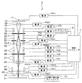
図1は、本発明の第1の実施の形態にかかる荷電ビーム露光装置の概略構成を示すブロック図である。本実施形態の特徴は、第1成形アパーチャ85に、面積および形状の少なくともいずれかが互いに異なる複数の開口が設けられている点と、描画パターンに要求される解像度に応じて第1成形アパーチャ85の開口が選択されるように、偏向器17,19に印加される電圧が制御される点にある。これらの特徴点は、後に詳述することとし、最初に本実施形態の荷電ビーム露光装置の構成および動作について概略的に説明する。
(1) First Embodiment FIG. 1 is a block diagram showing a schematic configuration of a charged beam exposure apparatus according to a first embodiment of the present invention. The feature of the present embodiment is that the
図1に示す電子ビーム露光装置1は、電子光学系と制御コンピュータ7と各種電源PS1〜7,PS11,PS13,PS15,PS17,PS21,PS23,PS25,PS27と2次電子検出器コントローラ31とを備える。
The electron
制御コンピュータ7は、装置全体を制御するとともに、後述する通り、選択偏向器17,19により第1成形アパーチャ85の任意の開口が選択されて電子ビームEBが照射されるように電源PS1,2を制御する。制御コンピュータ7は、本実施形態において、例えば偏向制御手段および焦点位置補正手段に対応する。
The
各種電源PS1〜7,PS11,PS13,PS15,PS17,PS21,PS23,PS25,PS27は、電子光学系の対応する各構成部分および制御コンピュータ7に接続され、制御コンピュータ7から与えられる制御信号に従い、これらの構成部分に電圧を印加する。
Various power supplies PS1 to 7, PS11, PS13, PS15, PS17, PS21, PS23, PS25, and PS27 are connected to the corresponding components of the electron optical system and the
2次電子検出器コントローラ31は、後述する2次電子検出器29および制御コンピュータ7に接続され、2次電子検出器29により検出された2次電子の信号を受け取って処理し、SEM(Scanning Electron Microscope)画像を構成する信号の形態で制御コンピュータ7に伝送する。
The secondary
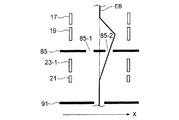
電子光学系は、電子ビームEBを発生させる電子銃11と、矩形または円形の開口を有する第1アパーチャ13と、照明レンズ15と、選択偏向器17,19と、本実施形態において特徴的な第1成形アパーチャ85と、ブランキング電極23−1,23−2と、振り戻し偏向器21と、ブランキングアパーチャ91と、投影レンズ93と、第1成形偏向器25と、第2成形アパーチャ95と、第2成形偏向器27と、縮小レンズ43と、副偏向器97と、主偏向器99と、対物レンズ45と、2次電子検出器29と、を含む。本実施形態において、投影レンズ93は、例えば投影手段に対応し、縮小レンズ43、および対物レンズ45は、例えば縮小投影手段に対応する。また、本実施形態において、選択偏向器17,19、および振り戻し偏向器21は、例えばそれぞれ第1乃至第3の偏向器に対応し、これらの偏向器17,19,21およびこれらにそれぞれ接続された電源PS1〜3は、例えば偏向手段に対応する。また、本実施形態において、ブランキング電極23−1,23−2とブランキングアパーチャ91とは、例えばブランキング手段に対応する。
The electron optical system includes an
照明レンズ15は、2個の静電レンズ(アインツェルレンズ)で構成され、それぞれ中央の電極へ電源PS21から負の電圧が印加されて使用され、第1成形アパーチャ85の開口に対して十分大きく、かつ、必要な大きさのビーム径となるように電子ビームEBの倍率を調整する。第1成形アパーチャ85には、面積および形状の少なくともいずれかが互いに異なる複数の矩形開口が設けられている。この点は、後に詳述する。
The
選択偏向器17,19は、照明レンズ13を通過した電子ビームEBが第1成形アパーチャ85の任意の矩形開口に入射するように、電子ビームEBを偏向制御する。
The
振り戻し偏向器21は、第1成形アパーチャ85を通過した電子ビームEBをその光軸上に振り戻す。
The
第1成形アパーチャ85を通過した電子ビームEBは、第1成形アパーチャ85を起点とする矩形ビームとして出発し、そのアパーチャ像は投影レンズ93によって第2成形アパーチャ95へ投影される。
The electron beam EB that has passed through the
ブランキング電極23−1,23−2は、電源PS13から印加される電圧による電界を励起することにより、電子ビームEBに対するブランキング偏向を行ない、ブランキングアパーチャ91と相俟って、電子ビームEBのウェーハS上へのオン・オフを制御する。
The blanking electrodes 23-1 and 23-2 perform blanking deflection on the electron beam EB by exciting an electric field by a voltage applied from the
第1成形偏向器25は、投影レンズ93を通過した電子ビームEBが第2成形アパーチャ95の所望の面積の所望のセルパターンに入射するように、CADデータに従って電子ビームEBを偏向制御する。第2成型偏向器27は、第2成形アパーチャ95を通過した電子ビームEBをその光軸上に振り戻す。
The
第1成形偏向器25、第2成形アパーチャ95および第2成型偏向器27を通過した電子ビームEBは、第2成形アパーチャ95を起点とするセルパターンビームとして出発し、光軸上に振り戻された状態で縮小レンズ43と対物レンズ45を通過してウェーハSに縮小投影される。縮小レンズ43は、第2成形アパーチャ95を起点とするセルパターン像を縮小させる。対物レンズ45は、縮小したセルパターン像をさらに縮小してウェーハS上に結像させる。
The electron beam EB that has passed through the first shaping
主偏向器99は、電源PS17から印加される電圧により、ウェーハSの描画領域(ストライプ)が走査されるように、電子ビームEBの軌道を偏向制御する。副偏向器97は、上記ストライプ内の領域をさらに細かく分割した描画範囲に対して電子ビームEBの照射位置を制御する。
The
2次電子検出器29は、対物レンズ45とウェーハSとの間に配置され、電子ビームEBの照射によりウェーハSの表面から発生する2次電子を検出する。2次電子検出器コントローラ31は、検出した信号を処理して制御コンピュータ7に供給し、この処理信号から制御コンピュータ7は、SEM像を検出し、ビーム調整等の制御に利用する。
The
図1では、光軸をZ方向と規定した場合のX−Z平面に沿った端面図を模した形態で電子光学系の構成を示した。電子光学系の各主要部の平面形状を図2に示す。同図では、これらの主要部間の位置関係を説明するために、各平面図のY軸が同一線上で重なるように紙面の上下に配列して示した。 In FIG. 1, the configuration of the electron optical system is shown in a form simulating an end view along the XZ plane when the optical axis is defined as the Z direction. The planar shape of each main part of the electron optical system is shown in FIG. In the figure, in order to explain the positional relationship between these main parts, they are shown arranged on the top and bottom of the paper surface so that the Y-axis of each plan view overlaps on the same line.
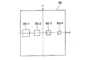
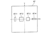
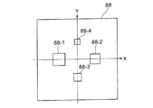
図1に示す電子ビーム露光装置1の電子光学系に設けられる第1成形アパーチャ85の平面図を図3に示す。同図に示す例では、面積が異なる2つの正方形の開口85−1,86−2がY軸を挟んでほぼ線対称になるようにX軸上に配設されている。荷電ビーム露光装置1の電子光学系に設置可能な第1成形アパーチャは図3に示す形状に限ることなく、面積および形状の少なくともいずれかが互いに異なる複数の矩形開口が設けられていれば良い。第1成形アパーチャの他の具体例を図4乃至図7の平面図に示す。図4に示す第1成形アパーチャ86では、X軸上の4つの正方形開口86−1乃至86−4が、紙面の左側から右側へ面積の大きい順から配設されている。図5に示す第1成形アパーチャ87では、中央付近でY軸にほぼ線対称になるようにX軸上に配置された2つの正方形開口87−2,87−3に加え、これらの正方形開口を挟むようにこれらの外側のX軸上に配置された2つの長方形開口87−1,87−4をさらに含む。長方形開口87−4の長手方向はX軸方向と一致するが、長方形開口87−1は、その長手方向がY軸方向になるように形成されている。図6に示す第1成形アパーチャ88は、X軸とY軸の交点を中心にほぼ回転対称をなすようにX軸およびY軸上にそれぞれ配置された4つの正方形開口88−1乃至88−4を含む。
FIG. 3 is a plan view of the
上述した4つの例では、いずれの開口もX軸上にまたはY軸上に配置されているが、この配置形態に限ることなく、例えば図7に示す第1成形アパーチャ89に示すように、X軸およびY軸から離れた位置に正方形または長方形の開口89−1,89−3,89−9を配置しても良い。さらに、開口を配置する方向も、特にX軸方向またはY軸方向に限ることなく、例えば図7の開口89−7,89−8のように任意の方向に配置することができる。
In the four examples described above, all the openings are arranged on the X axis or the Y axis. However, the present invention is not limited to this arrangement form. For example, as shown in the
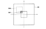
ここで、面積の大きな矩形開口を選択すれば、第1成形アパーチャを通過する電子ビームEBの電流量が大きくなり、一方、面積が小さい矩形開口を選択した場合は、第1成形アパーチャを通過する電子ビームEBの電流量が小さくなる。このような、第1成形アパーチャ85を通過する電子ビームEBの電流量の違いで空間電荷効果の発生量が異なり、第2成形アパーチャ95上でのフォーカスのズレ量が異なることにより、選択された開口次第では、フォーカスズレが大きく発生してしまい解像度が低下してしまうことがある。本実施形態では、制御コンピュータ7が第1成形アパーチャで選択される矩形開口の面積に応じて制御信号を生成して電源PS23に供給し、この制御信号に応答して、電源PS23が投影レンズ93に印加する電圧を調整する。これにより、第2成形アパーチャでのフォーカスズレが解消される。
Here, if a rectangular opening having a large area is selected, the amount of current of the electron beam EB passing through the first shaping aperture is increased. On the other hand, if a rectangular opening having a small area is selected, the current passes through the first shaping aperture. The amount of current of the electron beam EB is reduced. The amount of generation of the space charge effect differs depending on the difference in the amount of current of the electron beam EB passing through the
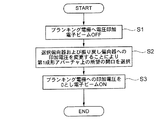
図8乃至図10を参照しながら、第1成形アパーチャに設けられた矩形開口の選択方法を説明する。図8は、矩形開口の具体的な選択手順を示すフローチャートであり、図9および図10は、選択された矩形開口を通過する荷電ビームの軌道を示す。 A method for selecting a rectangular opening provided in the first shaping aperture will be described with reference to FIGS. FIG. 8 is a flowchart showing a specific selection procedure of the rectangular aperture, and FIGS. 9 and 10 show the trajectory of the charged beam passing through the selected rectangular aperture.
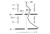
まず、電源PS13からブランキング電極23−1,23−2に電圧を印加することにより、ウェーハSに到達する電子ビームEBをオフにする(図8、ステップS1)。次に、選択する矩形開口に応じて電源PS1乃至PS3をそれぞれ調整して選択偏向器17,19および振り戻し偏向器21への印加電圧をそれぞれ変更することにより、選択した矩形開口に電子ビームEBを入射させる(図8、ステップS2)。最後に、ブランキング電極23−1,23−2への電源PS13の印加電圧をゼロにしてウェーハSに到達する電子ビームEBをオンにする(図8、ステップS3)。図9は、電子ビームEBをX軸方向に偏向して矩形開口85−2を選択したときのビーム軌道の一例を示す。図10は電子ビームEBをX軸方向に偏向して矩形開口85−1を選択したときのビーム軌道の一例を示す。
First, the electron beam EB reaching the wafer S is turned off by applying a voltage from the power source PS13 to the blanking electrodes 23-1 and 23-2 (FIG. 8, step S1). Next, by adjusting the power supplies PS1 to PS3 according to the rectangular opening to be selected and changing the applied voltages to the
面積の大きな矩形開口を選択すれば、第1成形アパーチャを通過する電子ビームEBの電流が大きいので、空間電荷効果によるビームぼけが大きく発生して解像度の点では劣るが、ショットサイズを大きくすることができるので、描画時間を短くすることができる。この一方、通過した電子ビームEBが第2成形アパーチャ95上の所望の領域を照明できる矩形開口のうち、例えば最も面積が小さい矩形開口を選択した場合は、ショットサイズが小さいために描画時間は長くかかってしまうが、通過するビーム電流の量が少ないので空間電荷効果によるビームぼけが小さくなり、これにより高解像度での描画が可能になる。このように、本実施形態によれば、面積および形状の少なくともいずれかが互いに異なる複数の開口から任意の開口を選択できるので、本来トレードオフの関係にある解像度と描画時間とを描画パターンの要求仕様に応じて調整することが可能になる。小さな開口を選択する場合には、例えば図11の斜線領域BMに示すように、従来の矩形開口を選択した場合(符号BMcに示す点線領域)と比較して、例えば第1成形アパーチャ85を通過して第2成形アパーチャ95で遮断されるビーム電流の量を少なくすることができるので、空間電荷効果によるビームぼけが抑制され、高分解能での描画が可能になる。
If a rectangular aperture with a large area is selected, the current of the electron beam EB passing through the first shaping aperture is large, resulting in large beam blur due to the space charge effect, which is inferior in terms of resolution, but increases the shot size. Since drawing is possible, drawing time can be shortened. On the other hand, when a rectangular opening having the smallest area is selected, for example, from among the rectangular openings that can illuminate a desired region on the
上述した矩形開口の選択工程のうち、例えば図8のフローチャートのステップS2において、選択偏向器17,19および振り戻し偏向器21への電圧印加は理論上では同時に実行される。しかしながら、現実には、各偏向器への印加電圧が異なっていることや、電源間の機差による電圧の立ち上がり時間および立ち下がり時間にばらつきが存在するためにブランキングエラーが発生することがある。特に、これらの電源電圧を高速で変化させた場合には、一時的に各偏向器間の印加電圧の極性や電圧比が崩れてしまうことがある。
Of the rectangular aperture selection process described above, for example, in step S2 of the flowchart of FIG. 8, voltage application to the
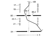
ブランキングエラーが発生する典型例として、ブランキング方向をX軸方向とし、第1成形アパーチャ85(図3参照)の矩形開口の選択も同様にX軸方向で変更した場合を挙げることができる。電子ビームEBをX軸方向にブランキングした状態で、X軸方向に配列された第1成形アパーチャ内の開口を選択すると、例えばそれぞれ図12および図13に示す通りのビーム軌道となる。このとき、所定のエラー条件が揃うと、例えば選択偏向器19の電圧が、選択偏向器17および振り戻し偏向器21よりも先に立ち上がってしまうと、ブランキングをしているにもかかわらず、電子ビームEBが例えば図14に示すようにブランキングアパーチャ91を通過してしまい、その結果、ウェーハS上のフォトレジストを感光してしまう。
As a typical example in which a blanking error occurs, a case where the blanking direction is the X-axis direction and the selection of the rectangular opening of the first shaping aperture 85 (see FIG. 3) is similarly changed in the X-axis direction can be cited. When the openings in the first shaping apertures arranged in the X-axis direction are selected in a state where the electron beam EB is blanked in the X-axis direction, for example, beam trajectories as shown in FIGS. 12 and 13 are obtained. At this time, if a predetermined error condition is met, for example, if the voltage of the
このようなブランキングエラーを回避するため、本実施形態では、第1成形アパーチャの矩形開口の選択方向と電子ビームEBのブランキング方向とが互いに直交するように、各電源を制御コンピュータ7が制御する。図15に示すように、例えばY軸方向にブランキングする場合には、第1成形アパーチャ内の矩形開口の選択方向をX軸方向にする。このように、本実施形態によれば、第1成形アパーチャ内の開口の選択軌道とブランキング軌道とをそれぞれ独立に制御することにより、ブランキングエラーを回避することができる。
In order to avoid such a blanking error, in this embodiment, the
(2)第2の実施の形態
図16は、本発明の第2の実施の形態にかかる荷電ビーム露光装置の概略構成を示すブロック図である。本実施形態は、要求される解像度に応じて第1成形アパーチャ内の任意の開口を上述したように選択する点に加え、前述したブランキングエラーを回避する他の手段を提供するものである。図1との対比により明らかなように、図16に示す電子ビーム露光装置2は、一端で制御コンピュータ7に接続され、他端で電源PS1〜PS3に接続されたタイミングコントローラ9をさらに備える。タイミングコントローラ9は、本実施形態において、例えばタイミング制御手段に対応し、制御コンピュータ7の指令信号を受け、選択偏向器17,19による選択偏向および振り戻し偏向器21による振り戻し偏向が互いに異なるタイミングで実行されるように電源PS1〜PS3による印加電圧の出力タイミングを調整する。本実施形態の電子ビーム露光装置2のその他の構成は、図1に示す電子ビーム露光装置1の構成と実質的に同一である。
(2) Second Embodiment FIG. 16 is a block diagram showing a schematic configuration of a charged beam exposure apparatus according to a second embodiment of the present invention. This embodiment provides other means for avoiding the above-described blanking error in addition to selecting an arbitrary opening in the first shaping aperture as described above according to the required resolution. As is clear from comparison with FIG. 1, the electron
タイミングコントローラ9による3つの偏向器17,19,21に対する偏向タイミングの制御動作について図面を参照しながら説明する。
The operation of controlling the deflection timing for the three
図17は、図16に示す電子ビーム露光装置2のタイミングコントローラ9による偏向タイミング制御の一例を示すタイミングチャートである。今、時刻T0において、電子ビームEBが第1成形アパーチャ85の矩形開口85−1を照明しており(図10参照、電子ビームEBがオン)、この状態から矩形開口85−2を照明する状態へ移行するものとする。まず、時刻T1にてタイミングコントローラ9から電源PS13に指令信号を与えてブランキング電圧VBKをブランキング電極23−1,23−2に印加させる。これにより、電子ビームEBが光軸から外側へ偏向されてブランキングアパーチャ91の開口を通らなくなる(図13参照、電子ビームEBがオフ)。次に、時刻T2において、電源PS2の出力電圧を0〔V〕とする制御信号がタイミングコントローラ9から電源PS2へ入力される。次いで、時刻T3において、電源PS1の出力電圧を−Va〔V〕へ低減させる制御信号がタイミングコントローラ9から電源PS1へ出力される。続いて、PS1の出力電圧が−Va〔V〕となる時刻T4のタイミングで電源PS2の出力電圧が0〔V〕から+Vb〔V〕へ上昇し始めるように制御信号がタイミングコントローラ9から電源PS2へ出力される。次いで、電源PS2の出力電圧が+Vb〔V〕となるタイミングT5で電源PS3の出力電圧が+Vc〔V〕から−Vc〔V〕へと低減するように制御信号がタイミングコントローラ9から電源PS3へ出力される。これにより、矩形開口85−2が選択された状態になる(図12参照)。さらに、時刻T7においてブランキング電極23−1,23−2に印加されるブランキング電圧が0となるように制御信号がタイミングコントローラ9から電源PS13に与えられ、これにより、電子ビームEBがブランキングアパーチャ91の開口を通ってウェーハSを照射するようになる(図9参照、電子ビームEBがオン)。
FIG. 17 is a timing chart showing an example of deflection timing control by the timing controller 9 of the electron
矩形開口85−2から85−1へと選択を変更するときのタイミング制御は、上記手順とほぼ逆の手順を実行すれば良い。即ち、時刻T8で電源PS13への印加電圧を0〔V〕から+VBK〔V〕へ上昇させて電子ビームEBをオフにする(図12参照)。時刻T9で、電源PS3の出力電圧の上昇を開始させる。電源PS3の出力電圧が−Vc〔V〕から+Vc〔V〕へ到達した時刻T10で電源PS2の出力電圧を+Vb〔V〕から0〔V〕へと低減させる。電源PS2の出力電圧が0〔V〕になった時刻T11で、電源PS1の出力電圧の上昇を開始させる。電源PS1の出力電圧が+Va〔V〕に達した時刻T12において、電源PS2の出力電圧を0〔V〕から−Vb〔V〕へ低減させる。これにより、第1成形アパーチャ85の矩形開口85−1が選択された状態になる(図13参照)。最後に時刻T13において、電源PS13への印加電圧を+VBK〔V〕から0〔V〕へ低減させ、これにより、電子ビームEBがオンとなって、電子ビームEBがブランキングアパーチャ91の開口を通ってウェーハSを照射する(図10参照)。
The timing control when changing the selection from the rectangular opening 85-2 to 85-1 may be performed by executing a procedure that is almost the reverse of the above procedure. That is, the applied voltage at time T 8 to the power supply PS13 is raised to 0 [V] to + V BK [V] to turn off the electron beam EB (see FIG. 12). At time T 9, and starts a rise in the output voltage of the power supply PS3. The output voltage of the power source PS3 is reduced and the output voltage of the power source PS2 + from Vb [V] at time T 10 arriving from -Vc [V] + Vc to [V] to 0 [V]. At time T 11 the output voltage of the power source PS2 becomes 0 [V], to initiate an increase in the output voltage of the power supply PS1. At time T 12 the output voltage reaches the + Va [V] power source PS1, reduce the output voltage of the power source PS2 from 0 [V] to -Vb [V]. Thereby, the rectangular opening 85-1 of the 1st shaping | molding
本実施形態によれば、例えば図6に示す第1成形アパーチャ88を使用する場合など、X軸方向とY軸方向のいずれの方向にも矩形開口の選択が実行される場合でも、ブランキングエラーを確実に回避することができる。 According to the present embodiment, for example, when the first shaping aperture 88 shown in FIG. 6 is used, even when the rectangular opening is selected in either the X-axis direction or the Y-axis direction, a blanking error occurs. Can be reliably avoided.
(3)半導体装置の製造方法
上述した第1の実施形態における荷電ビームの制御方法を用いて基板にパターンを描画することにより、高い解像度が要求される場合には、第1成形アパーチャと第2成形アパーチャとの間で生じ得る空間電荷効果の影響を低減でき、この一方、高い解像度が要求されない場合には、ショットサイズを大きくして描画時間を短縮することができ、要求仕様に応じた解像度でパターン描画を行なうことができる。これにより、半導体装置の製造において製品精度と製造コストとのトレードオフの関係に柔軟に対処することができる。
(3) Manufacturing Method of Semiconductor Device When a high resolution is required by drawing a pattern on the substrate using the charged beam control method in the first embodiment described above, the first shaping aperture and the second The space charge effect that can occur with the molding aperture can be reduced. On the other hand, when high resolution is not required, the shot time can be increased to shorten the drawing time, and the resolution according to the required specifications. The pattern can be drawn with. Thereby, it is possible to flexibly cope with a trade-off relationship between product accuracy and manufacturing cost in manufacturing a semiconductor device.
また、上述した第2の実施形態における荷電ビームの制御方法を用いて基板にパターンを描画することにより、ブランキング偏向におけるエラーを的確に回避することができるので、高い歩留まりで半導体装置を製造することが可能になる。 Further, by drawing a pattern on the substrate using the charged beam control method according to the second embodiment described above, errors in blanking deflection can be avoided accurately, so that a semiconductor device is manufactured with a high yield. It becomes possible.
以上、本発明の実施の形態のいくつかについて説明したが、本発明は上記形態に限られることなく、その技術的範囲内で種々変更して実施可能であることは勿論である。例えば、上述した実施形態では、2段の選択偏向器と1段の振り戻し偏向器を用いて第1成形アパーチャ内の矩形開口を選択する形態について説明した。しかしながら、偏向器の数量は上記組み合わせに限るものではなく、例えば2段の選択偏向器と2段の振り戻し偏向器を用いて開口の選択を行なっても良い。この場合も、上述したブランキングエラー回避方法のいずれを適用しても電子ビームEBの漏れを回避することができる。選択偏向器および振り戻し偏向器は、特に限定されることなく、静電型でも磁界型でも用いることができる。 While some of the embodiments of the present invention have been described above, the present invention is not limited to the above-described embodiments, and can of course be implemented with various modifications within the technical scope thereof. For example, in the above-described embodiment, the form in which the rectangular opening in the first shaping aperture is selected using the two-stage selection deflector and the one-stage swing back deflector has been described. However, the number of deflectors is not limited to the above combination. For example, the aperture may be selected using a two-stage selection deflector and a two-stage swing back deflector. Also in this case, leakage of the electron beam EB can be avoided by applying any of the blanking error avoidance methods described above. The selection deflector and the swing back deflector are not particularly limited, and can be either an electrostatic type or a magnetic type.
1,2 電子ビーム露光装置
7 制御コンピュータ
9 タイミングコントローラ
11 電子銃
13 第1アパーチャ
15 照明レンズ
17,19 選択偏向器
21 振り戻し偏向器
23−1,23−2 ブランキング電極
25 第1成型偏向器
27 第2成型偏向器
29 2次電子検出器
31 2次電子検出器コントローラ
43 縮小レンズ
45 対物レンズ
85〜89 第1成型アパーチャ
91 ブランキングアパーチャ
93 投影レンズ
95 第2成型アパーチャ
97 副偏向器
99 主偏向器
EB 電子ビーム
PS1〜7,PS11,PS13,PS15,PS17,PS21,PS23,PS25,PS27 電源
S ウェーハ
DESCRIPTION OF
Claims (12)
基板への描画パターンに対応した形状のパターンが設けられた第2成形アパーチャと、
荷電ビームを生成して前記第1成形アパーチャに照射させる荷電ビーム生成手段と、
前記第1成形アパーチャの任意の開口を通過した前記荷電ビームを前記第2成形アパーチャ上に投影する投影手段と、
前記荷電ビーム生成手段と前記投影手段との間に設けられ、前記荷電ビームを偏向する偏向手段と、
通過する前記荷電ビームの前記第2成形アパーチャ上の所望の領域への照明を可能にする前記第1成形アパーチャの開口のうちで最も面積の小さな開口が選択されるように前記偏向手段を制御する偏向制御手段と、
前記第2成形アパーチャを通過した前記荷電ビームを前記基板上に縮小投影する縮小投影手段と、
を備える荷電ビーム露光装置。 A first shaping aperture provided with a plurality of rectangular openings having at least one of area and shape different from each other;
A second shaping aperture provided with a pattern having a shape corresponding to a drawing pattern on the substrate;
Charged beam generating means for generating a charged beam and irradiating the first shaping aperture;
Projecting means for projecting the charged beam that has passed through any opening of the first shaping aperture onto the second shaping aperture;
A deflecting means provided between the charged beam generating means and the projecting means for deflecting the charged beam;
The deflecting means is controlled so that the opening having the smallest area among the openings of the first shaping aperture that enables illumination of a desired region on the second shaping aperture of the charged beam passing therethrough is selected. Deflection control means;
Reduction projection means for reducing and projecting the charged beam that has passed through the second shaping aperture onto the substrate;
A charged beam exposure apparatus.
基板への描画パターンに対応した形状のパターンが設けられた第2成形アパーチャと、
荷電ビームを生成して前記第1成形アパーチャに照射させる荷電ビーム生成手段と、
前記第1成形アパーチャの任意の開口を通過した前記荷電ビームを前記第2成形アパーチャ上に投影する投影手段と、
前記荷電ビーム生成手段と前記投影手段との間に設けられ、前記荷電ビームを偏向する偏向手段と、
前記荷電ビームが、前記描画パターンに要求される解像度に応じて前記開口が選択されるように前記偏向手段を制御する偏向制御手段と、
前記第2成形アパーチャを通過した前記荷電ビームを前記基板上に縮小投影する縮小投影手段と、
を備える荷電ビーム露光装置。 A first shaping aperture provided with a plurality of rectangular openings having at least one of area and shape different from each other;
A second shaping aperture provided with a pattern having a shape corresponding to a drawing pattern on the substrate;
Charged beam generating means for generating a charged beam and irradiating the first shaping aperture;
Projecting means for projecting the charged beam that has passed through any opening of the first shaping aperture onto the second shaping aperture;
A deflecting means provided between the charged beam generating means and the projecting means for deflecting the charged beam;
Deflection control means for controlling the deflection means such that the aperture is selected according to the resolution required for the drawing pattern of the charged beam;
Reduction projection means for reducing and projecting the charged beam that has passed through the second shaping aperture onto the substrate;
A charged beam exposure apparatus.
基板への描画パターンに対応した形状のパターンが設けられた第2成形アパーチャと、
荷電ビームを生成して前記第1成形アパーチャに照射させる荷電ビーム生成手段と、
前記第1成形アパーチャの任意の開口を通過した前記荷電ビームを前記第2成形アパーチャ上に投影する投影手段と、
前記荷電ビーム生成手段と前記投影手段との間に設けられ、前記荷電ビームを偏向する偏向手段と、
前記荷電ビームのうち前記第2成形アパーチャによって遮断される部分の電流量が最小となる前記開口が選択されるように前記偏向手段を制御する偏向制御手段と、
前記第2成形アパーチャを通過した前記荷電ビームを前記基板上に縮小投影する縮小投影手段と、
を備える荷電ビーム露光装置。 A first shaping aperture provided with a plurality of rectangular openings having at least one of area and shape different from each other;
A second shaping aperture provided with a pattern having a shape corresponding to a drawing pattern on the substrate;
Charged beam generating means for generating a charged beam and irradiating the first shaping aperture;
Projecting means for projecting the charged beam that has passed through any opening of the first shaping aperture onto the second shaping aperture;
A deflecting means provided between the charged beam generating means and the projecting means for deflecting the charged beam;
Deflection control means for controlling the deflection means so as to select the opening that minimizes the amount of current in a portion of the charged beam that is blocked by the second shaping aperture;
Reduction projection means for reducing and projecting the charged beam that has passed through the second shaping aperture onto the substrate;
A charged beam exposure apparatus.
基板への描画パターンに対応した形状のパターンが設けられた第2成形アパーチャと、
荷電ビームを生成して前記第1成形アパーチャに照射させる荷電ビーム生成手段と、
前記第1成形アパーチャの任意の開口を通過した前記荷電ビームを前記第2成形アパーチャ上に投影する投影手段と、
前記荷電ビーム生成手段と前記投影手段との間に設けられ、前記荷電ビームを偏向する偏向手段と、
前記荷電ビームを偏向することにより前記基板への照射のオンとオフとを選択的に制御するブランキング手段と、
前記ブランキング手段による偏向方向と直交する方向へ前記荷電ビームが偏向されて前記任意の開口を選択的に通過するように前記偏向手段を制御する偏向制御手段と、
前記第2成形アパーチャを通過した前記荷電ビームを前記基板上に縮小投影する縮小投影手段と、
を備える荷電ビーム露光装置。 A first shaping aperture provided with a plurality of rectangular openings having at least one of area and shape different from each other;
A second shaping aperture provided with a pattern having a shape corresponding to a drawing pattern on the substrate;
Charged beam generating means for generating a charged beam and irradiating the first shaping aperture;
Projecting means for projecting the charged beam that has passed through any opening of the first shaping aperture onto the second shaping aperture;
A deflecting means provided between the charged beam generating means and the projecting means for deflecting the charged beam;
Blanking means for selectively controlling on and off of irradiation to the substrate by deflecting the charged beam;
Deflection control means for controlling the deflection means so that the charged beam is deflected in a direction orthogonal to the deflection direction by the blanking means and selectively passes through the arbitrary opening;
Reduction projection means for reducing and projecting the charged beam that has passed through the second shaping aperture onto the substrate;
A charged beam exposure apparatus.
基板への描画パターンに対応した形状のパターンが設けられた第2成形アパーチャと、
荷電ビームを生成して前記第1成形アパーチャに照射させる荷電ビーム生成手段と、
前記第1成形アパーチャの任意の開口を通過した前記荷電ビームを前記第2成形アパーチャ上に投影する投影手段と、
前記第2成形アパーチャを通過した前記荷電ビームを前記基板上に縮小投影する縮小投影手段と、
前記荷電ビームを偏向することにより前記基板への照射のオンとオフとを選択的に制御するブランキング手段と、
前記荷電ビームが任意の前記開口を選択的に通過するように前記偏向手段を制御する偏向制御手段と、
前記荷電ビームの光軸方向において前記第1成形アパーチャよりも前記荷電ビーム生成手段側に配設されて前記荷電ビームを偏向することにより任意の前記開口に照射させる第1および第2の偏向器と、前記第1成形アパーチャよりも前記基板側に配設されて前記開口を通過した前記荷電ビームを前記光軸側に振り戻す第3の偏向器と、を含む偏向手段と、
前記第1乃至第3の偏向器が互いに異なるタイミングで動作するように前記偏向手段を制御するタイミング制御手段と、
を備える荷電ビーム露光装置。 A first shaping aperture provided with a plurality of rectangular openings having at least one of area and shape different from each other;
A second shaping aperture provided with a pattern having a shape corresponding to a drawing pattern on the substrate;
Charged beam generating means for generating a charged beam and irradiating the first shaping aperture;
Projecting means for projecting the charged beam that has passed through any opening of the first shaping aperture onto the second shaping aperture;
Reduction projection means for reducing and projecting the charged beam that has passed through the second shaping aperture onto the substrate;
Blanking means for selectively controlling on and off of irradiation to the substrate by deflecting the charged beam;
Deflection control means for controlling the deflection means so that the charged beam selectively passes through any of the openings;
First and second deflectors disposed on the charged beam generating means side of the first shaping aperture in the optical axis direction of the charged beam and deflecting the charged beam to irradiate an arbitrary aperture; And a third deflector disposed on the substrate side of the first shaping aperture and for returning the charged beam that has passed through the opening to the optical axis side,
Timing control means for controlling the deflecting means so that the first to third deflectors operate at different timings;
A charged beam exposure apparatus.
前記第1成形アパーチャの前記任意の開口を通過した前記荷電ビームを、基板への描画パターンに対応した形状のパターンが設けられた第2成形アパーチャに投影する投影工程と、
前記第2成形アパーチャの前記パターンを通過した前記荷電ビームを前記基板上に縮小投影する縮小投影工程と、
通過後に前記第2成形アパーチャ上の所望の領域への前記荷電ビームの照明を可能にする前記第1成形アパーチャの開口のうちで最も面積の小さな開口を前記荷電ビームが選択的に通過するように前記荷電ビームを偏向する偏向工程と、
を備える荷電ビームの制御方法。 A charged beam generating step of generating a charged beam and irradiating an arbitrary opening of a first shaping aperture provided with a plurality of rectangular openings having different areas and shapes from each other;
A projection step of projecting the charged beam that has passed through the arbitrary opening of the first shaping aperture onto a second shaping aperture provided with a pattern having a shape corresponding to a drawing pattern on a substrate;
A reduction projection step of reducing and projecting the charged beam that has passed through the pattern of the second shaping aperture onto the substrate;
The charged beam selectively passes through an aperture having the smallest area among the apertures of the first shaping aperture that enables illumination of the charged beam to a desired region on the second shaping aperture after passing. A deflection step of deflecting the charged beam;
A charged beam control method comprising:
前記第1成形アパーチャの前記任意の開口を通過した前記荷電ビームを、基板への描画パターンに対応した形状のパターンが設けられた第2成形アパーチャに投影する投影工程と、
前記第2成形アパーチャの前記パターンを通過した前記荷電ビームを前記基板上に縮小投影する縮小投影工程と、
発生した前記荷電ビームが前記描画パターンに要求される解像度に応じて前記開口が選択されるように前記荷電ビームを偏向する偏向工程と、
を備える荷電ビームの制御方法。 A charged beam generating step of generating a charged beam and irradiating an arbitrary opening of a first shaping aperture provided with a plurality of rectangular openings having different areas and shapes from each other;
A projection step of projecting the charged beam that has passed through the arbitrary opening of the first shaping aperture onto a second shaping aperture provided with a pattern having a shape corresponding to a drawing pattern on a substrate;
A reduction projection step of reducing and projecting the charged beam that has passed through the pattern of the second shaping aperture onto the substrate;
A deflection step of deflecting the charged beam such that the generated beam is selected according to a resolution required for the drawing pattern;
A charged beam control method comprising:
前記第1成形アパーチャの前記任意の開口を通過した前記荷電ビームを、基板への描画パターンに対応した形状のパターンが設けられた第2成形アパーチャに投影する投影工程と、
前記第2成形アパーチャの前記パターンを通過した前記荷電ビームを前記基板上に縮小投影する縮小投影工程と、
前記荷電ビームのうち前記第2成形アパーチャによって遮断される部分の電流量が最小となる前記開口が選択されるように前記荷電ビームを偏向する偏向工程と、
を備える荷電ビームの制御方法。 A charged beam generating step of generating a charged beam and irradiating an arbitrary opening of a first shaping aperture provided with a plurality of rectangular openings having different areas and shapes from each other;
A projection step of projecting the charged beam that has passed through the arbitrary opening of the first shaping aperture onto a second shaping aperture provided with a pattern having a shape corresponding to a drawing pattern on a substrate;
A reduction projection step of reducing and projecting the charged beam that has passed through the pattern of the second shaping aperture onto the substrate;
A deflection step of deflecting the charged beam such that the opening that minimizes the amount of current in a portion of the charged beam blocked by the second shaping aperture is selected;
A charged beam control method comprising:
前記第1成形アパーチャの前記任意の開口を通過した前記荷電ビームを、基板への描画パターンに対応した形状のパターンが設けられた第2成形アパーチャに投影する投影工程と、
前記第2成形アパーチャの前記パターンを通過した前記荷電ビームを前記基板上に縮小投影する縮小投影工程と、
前記荷電ビームを偏向することにより前記基板への照射のオンとオフとを選択的に制御するブランキング偏向工程と、
発生した前記荷電ビームが前記第1成形アパーチャの前記任意の開口を選択的に通過するように前記ブランキング偏向工程による偏向方向に直交する方向に前記荷電ビームを偏向する偏向工程と、
を備える、荷電ビームの制御方法。 A charged beam generating step of generating a charged beam and irradiating an arbitrary opening of the first shaping aperture provided with a plurality of openings;
A projection step of projecting the charged beam that has passed through the arbitrary opening of the first shaping aperture onto a second shaping aperture provided with a pattern having a shape corresponding to a drawing pattern on a substrate;
A reduction projection step of reducing and projecting the charged beam that has passed through the pattern of the second shaping aperture onto the substrate;
A blanking deflection step for selectively controlling on and off of irradiation to the substrate by deflecting the charged beam;
A deflection step of deflecting the charged beam in a direction orthogonal to a deflection direction of the blanking deflection step so that the generated charged beam selectively passes through the arbitrary opening of the first shaping aperture;
A method for controlling a charged beam.
前記第1成形アパーチャの前記任意の開口を通過した前記荷電ビームを、基板への描画パターンに対応した形状のパターンが設けられた第2成形アパーチャに投影する投影工程と、
前記第2成形アパーチャの前記パターンを通過した前記荷電ビームを前記基板上に縮小投影する縮小投影工程と、
前記荷電ビームを偏向することにより前記基板への照射のオンとオフとを選択的に制御するブランキング偏向工程と、
発生した前記荷電ビームが前記第1成形アパーチャの前記任意の開口を選択的に通過するように前記荷電ビームを偏向する第1および第2の偏向工程と、前記任意の開口を通過した前記荷電ビームを前記光軸側に振り戻す第3の偏向工程と、を含む偏向工程と、
前記第1乃至第3の偏向工程が互いに異なるタイミングで実行されるように前記偏向工程を制御する偏向制御工程と、
を備える荷電ビームの制御方法。 A charged beam generating step of generating a charged beam and irradiating an arbitrary opening of the first shaping aperture provided with a plurality of openings;
A projection step of projecting the charged beam that has passed through the arbitrary opening of the first shaping aperture onto a second shaping aperture provided with a pattern having a shape corresponding to a drawing pattern on a substrate;
A reduction projection step of reducing and projecting the charged beam that has passed through the pattern of the second shaping aperture onto the substrate;
A blanking deflection step for selectively controlling on and off of irradiation to the substrate by deflecting the charged beam;
First and second deflection steps for deflecting the charged beam so that the generated charged beam selectively passes through the arbitrary opening of the first shaping aperture, and the charged beam that has passed through the arbitrary opening. A third deflection step of swinging back to the optical axis side,
A deflection control step for controlling the deflection step so that the first to third deflection steps are executed at different timings;
A charged beam control method comprising:
Priority Applications (2)
| Application Number | Priority Date | Filing Date | Title |
|---|---|---|---|
| JP2004318193A JP2006128564A (en) | 2004-11-01 | 2004-11-01 | Charged beam exposure apparatus and charged beam control method |
| US11/260,251 US7304320B2 (en) | 2004-11-01 | 2005-10-28 | Charged beam exposure apparatus, charged beam control method and manufacturing method of semiconductor device |
Applications Claiming Priority (1)
| Application Number | Priority Date | Filing Date | Title |
|---|---|---|---|
| JP2004318193A JP2006128564A (en) | 2004-11-01 | 2004-11-01 | Charged beam exposure apparatus and charged beam control method |
Publications (1)
| Publication Number | Publication Date |
|---|---|
| JP2006128564A true JP2006128564A (en) | 2006-05-18 |
Family
ID=36460117
Family Applications (1)
| Application Number | Title | Priority Date | Filing Date |
|---|---|---|---|
| JP2004318193A Pending JP2006128564A (en) | 2004-11-01 | 2004-11-01 | Charged beam exposure apparatus and charged beam control method |
Country Status (2)
| Country | Link |
|---|---|
| US (1) | US7304320B2 (en) |
| JP (1) | JP2006128564A (en) |
Cited By (2)
| Publication number | Priority date | Publication date | Assignee | Title |
|---|---|---|---|---|
| US7759659B2 (en) | 2007-08-29 | 2010-07-20 | Nuflare Technology, Inc. | Charged particle beam writing method |
| KR101428620B1 (en) * | 2012-02-16 | 2014-08-08 | 가부시키가이샤 뉴플레어 테크놀로지 | Electron beam writing apparatus and electron beam writing method |
Families Citing this family (7)
| Publication number | Priority date | Publication date | Assignee | Title |
|---|---|---|---|---|
| JP2006128564A (en) * | 2004-11-01 | 2006-05-18 | Toshiba Corp | Charged beam exposure apparatus and charged beam control method |
| JP5634052B2 (en) * | 2009-01-09 | 2014-12-03 | キヤノン株式会社 | Charged particle beam drawing apparatus and device manufacturing method |
| US9134616B2 (en) * | 2009-10-12 | 2015-09-15 | Mentor Graphics Corporation | Generalization of shot definitions for mask and wafer writing tools |
| WO2011055521A1 (en) * | 2009-11-06 | 2011-05-12 | 株式会社日立ハイテクノロジーズ | Charged particle microscope |
| JP5506560B2 (en) * | 2010-06-18 | 2014-05-28 | キヤノン株式会社 | Drawing apparatus and device manufacturing method |
| RU2014115699A (en) * | 2011-09-19 | 2015-10-27 | МЭППЕР ЛИТОГРАФИ АйПи Б.В. | METHOD AND DEVICE FOR FORECASTING GROWTH SPEED OF DEPOSITED POLLUTANTS |
| JP6349944B2 (en) * | 2014-05-13 | 2018-07-04 | 株式会社ニューフレアテクノロジー | Electron beam drawing apparatus and electron beam drawing method |
Citations (18)
| Publication number | Priority date | Publication date | Assignee | Title |
|---|---|---|---|---|
| JPS5435173U (en) * | 1977-08-12 | 1979-03-07 | ||
| JPS5469075A (en) * | 1977-11-14 | 1979-06-02 | Hitachi Ltd | Electron beam drawing device |
| JPS5712521A (en) * | 1980-06-26 | 1982-01-22 | Nippon Telegr & Teleph Corp <Ntt> | Drawing device of figure by electron beam |
| JPS583228A (en) * | 1981-06-30 | 1983-01-10 | Toshiba Corp | Charged beam optical lens-barrel |
| JPS63114125A (en) * | 1986-10-31 | 1988-05-19 | Toshiba Corp | Charged beam exposure device |
| JPH04137520A (en) * | 1990-09-28 | 1992-05-12 | Hitachi Ltd | Device and method for electron beam lithography |
| JPH08153658A (en) * | 1994-11-28 | 1996-06-11 | Hitachi Ltd | Electron beam drawing method and apparatus |
| JPH1074682A (en) * | 1996-08-30 | 1998-03-17 | Nec Corp | Electron beam lithography system |
| JPH1079335A (en) * | 1996-09-04 | 1998-03-24 | Hitachi Ltd | Electron beam drawing equipment |
| JPH10255712A (en) * | 1997-03-07 | 1998-09-25 | Nec Corp | Electron beam exposure apparatus and its exposure method |
| JP2000173529A (en) * | 1997-12-19 | 2000-06-23 | Toshiba Corp | Electron beam writing method and apparatus |
| JP2000243683A (en) * | 1999-02-18 | 2000-09-08 | Nec Corp | Electron beam exposure apparatus and electron beam exposure method |
| JP2001118771A (en) * | 1999-10-18 | 2001-04-27 | Nec Corp | Charged particle beam drawing apparatus and charged particle beam drawing method |
| JP2002050567A (en) * | 2000-08-04 | 2002-02-15 | Toshiba Corp | Charged beam exposure equipment |
| JP2002353128A (en) * | 2001-05-30 | 2002-12-06 | Hitachi Ltd | Electron beam writing apparatus and electron beam writing method |
| JP2004047766A (en) * | 2002-07-12 | 2004-02-12 | Toshiba Corp | Electron beam exposure control method and apparatus |
| JP2004304031A (en) * | 2003-03-31 | 2004-10-28 | Toshiba Corp | Mask scan drawing method |
| JP2006126823A (en) * | 2004-09-30 | 2006-05-18 | Fujitsu Ltd | Variable rectangular electron beam exposure apparatus and pattern exposure / formation method |
Family Cites Families (17)
| Publication number | Priority date | Publication date | Assignee | Title |
|---|---|---|---|---|
| US5173582A (en) * | 1988-10-31 | 1992-12-22 | Fujitsu Limited | Charged particle beam lithography system and method |
| US5843603A (en) * | 1995-08-25 | 1998-12-01 | Kabushiki Kaisha Toshiba | Method of evaluating shaped beam of charged beam writer and method of forming pattern |
| JPH1140475A (en) * | 1997-07-18 | 1999-02-12 | Nec Corp | Exposure / drawing apparatus, exposure / drawing method, and recording medium storing exposure / drawing processing program |
| JP3508622B2 (en) * | 1999-05-20 | 2004-03-22 | 株式会社日立製作所 | Electron beam drawing apparatus and drawing method using electron beam |
| US6822248B2 (en) * | 2001-03-15 | 2004-11-23 | International Business Machines Corporation | Spatial phase locking with shaped electron beam lithography |
| JP2002299207A (en) * | 2001-03-29 | 2002-10-11 | Toshiba Corp | Charged particle beam writing system |
| JP3816815B2 (en) * | 2001-09-27 | 2006-08-30 | 株式会社東芝 | Charged particle beam exposure method and charged particle beam exposure data creation method |
| JP2003148915A (en) * | 2001-11-13 | 2003-05-21 | Jeol Ltd | Pattern connection accuracy inspection method |
| JP3626453B2 (en) * | 2001-12-27 | 2005-03-09 | 株式会社東芝 | Photomask correction method and correction apparatus |
| JP4074240B2 (en) * | 2003-09-30 | 2008-04-09 | 株式会社東芝 | Deflection distortion correction system, deflection distortion correction method, deflection distortion correction program, and semiconductor device manufacturing method |
| JP4313145B2 (en) * | 2003-10-07 | 2009-08-12 | 株式会社日立ハイテクノロジーズ | Charged particle beam drawing method and charged particle beam drawing apparatus |
| JP3968338B2 (en) * | 2003-10-08 | 2007-08-29 | 株式会社東芝 | Charged beam exposure system |
| JP3889743B2 (en) * | 2003-12-05 | 2007-03-07 | 株式会社東芝 | Charged beam drawing method and drawing apparatus |
| JP2006024624A (en) * | 2004-07-06 | 2006-01-26 | Toshiba Corp | Charged beam drawing apparatus and aperture adjustment method |
| JP4737968B2 (en) * | 2004-10-13 | 2011-08-03 | 株式会社東芝 | Correction device, correction method, correction program, and semiconductor device manufacturing method |
| JP2006128564A (en) * | 2004-11-01 | 2006-05-18 | Toshiba Corp | Charged beam exposure apparatus and charged beam control method |
| JP2006294794A (en) * | 2005-04-08 | 2006-10-26 | Toshiba Corp | Electron beam exposure apparatus and electron beam exposure method |
-
2004
- 2004-11-01 JP JP2004318193A patent/JP2006128564A/en active Pending
-
2005
- 2005-10-28 US US11/260,251 patent/US7304320B2/en not_active Expired - Fee Related
Patent Citations (18)
| Publication number | Priority date | Publication date | Assignee | Title |
|---|---|---|---|---|
| JPS5435173U (en) * | 1977-08-12 | 1979-03-07 | ||
| JPS5469075A (en) * | 1977-11-14 | 1979-06-02 | Hitachi Ltd | Electron beam drawing device |
| JPS5712521A (en) * | 1980-06-26 | 1982-01-22 | Nippon Telegr & Teleph Corp <Ntt> | Drawing device of figure by electron beam |
| JPS583228A (en) * | 1981-06-30 | 1983-01-10 | Toshiba Corp | Charged beam optical lens-barrel |
| JPS63114125A (en) * | 1986-10-31 | 1988-05-19 | Toshiba Corp | Charged beam exposure device |
| JPH04137520A (en) * | 1990-09-28 | 1992-05-12 | Hitachi Ltd | Device and method for electron beam lithography |
| JPH08153658A (en) * | 1994-11-28 | 1996-06-11 | Hitachi Ltd | Electron beam drawing method and apparatus |
| JPH1074682A (en) * | 1996-08-30 | 1998-03-17 | Nec Corp | Electron beam lithography system |
| JPH1079335A (en) * | 1996-09-04 | 1998-03-24 | Hitachi Ltd | Electron beam drawing equipment |
| JPH10255712A (en) * | 1997-03-07 | 1998-09-25 | Nec Corp | Electron beam exposure apparatus and its exposure method |
| JP2000173529A (en) * | 1997-12-19 | 2000-06-23 | Toshiba Corp | Electron beam writing method and apparatus |
| JP2000243683A (en) * | 1999-02-18 | 2000-09-08 | Nec Corp | Electron beam exposure apparatus and electron beam exposure method |
| JP2001118771A (en) * | 1999-10-18 | 2001-04-27 | Nec Corp | Charged particle beam drawing apparatus and charged particle beam drawing method |
| JP2002050567A (en) * | 2000-08-04 | 2002-02-15 | Toshiba Corp | Charged beam exposure equipment |
| JP2002353128A (en) * | 2001-05-30 | 2002-12-06 | Hitachi Ltd | Electron beam writing apparatus and electron beam writing method |
| JP2004047766A (en) * | 2002-07-12 | 2004-02-12 | Toshiba Corp | Electron beam exposure control method and apparatus |
| JP2004304031A (en) * | 2003-03-31 | 2004-10-28 | Toshiba Corp | Mask scan drawing method |
| JP2006126823A (en) * | 2004-09-30 | 2006-05-18 | Fujitsu Ltd | Variable rectangular electron beam exposure apparatus and pattern exposure / formation method |
Cited By (4)
| Publication number | Priority date | Publication date | Assignee | Title |
|---|---|---|---|---|
| US7759659B2 (en) | 2007-08-29 | 2010-07-20 | Nuflare Technology, Inc. | Charged particle beam writing method |
| USRE44179E1 (en) | 2007-08-29 | 2013-04-30 | Nuflare Technology, Inc. | Charged particle beam writing method |
| KR101428620B1 (en) * | 2012-02-16 | 2014-08-08 | 가부시키가이샤 뉴플레어 테크놀로지 | Electron beam writing apparatus and electron beam writing method |
| US8816276B2 (en) | 2012-02-16 | 2014-08-26 | Nuflare Technology, Inc. | Electron beam writing apparatus and electron beam writing method |
Also Published As
| Publication number | Publication date |
|---|---|
| US7304320B2 (en) | 2007-12-04 |
| US20060108546A1 (en) | 2006-05-25 |
Similar Documents
| Publication | Publication Date | Title |
|---|---|---|
| JP5634052B2 (en) | Charged particle beam drawing apparatus and device manufacturing method | |
| JP4995261B2 (en) | Particle beam exposure system with total modulation of patterned beam | |
| US8122390B2 (en) | Charged particle beam writing apparatus, and apparatus and method for correcting dimension error of pattern | |
| CN1645548B (en) | Charged particle beam device | |
| US10451976B2 (en) | Electron beam irradiation apparatus and electron beam dynamic focus adjustment method | |
| JP2008004597A (en) | Charged particle beam drawing method, exposure apparatus, and device manufacturing method | |
| JP3993334B2 (en) | Charged beam lithography system | |
| US8431908B2 (en) | Charged particle beam writing apparatus and charged particle beam writing method | |
| CN110571116B (en) | Charged particle beam drawing device and charged particle beam drawing method | |
| US20020033458A1 (en) | Charged particle beam exposure system | |
| JP4612838B2 (en) | Charged particle beam exposure apparatus and exposure method therefor | |
| JP5607413B2 (en) | Charged particle beam drawing apparatus and charged particle beam drawing method | |
| JP2001015430A (en) | Electron beam projection lithography system with multiple apertures | |
| JP2006128564A (en) | Charged beam exposure apparatus and charged beam control method | |
| JP2017028284A (en) | Charged particle beam drawing apparatus, control method thereof, and correction drawing data creation method | |
| JP2015035563A (en) | Drawing data generation method, processing device, program, drawing device, and article manufacturing method | |
| US10504686B2 (en) | Charged particle beam writing method and charged particle beam writing apparatus | |
| JP2005032837A (en) | Charged particle drawing method and device manufacturing method using the method | |
| JP3968338B2 (en) | Charged beam exposure system | |
| JP4458372B2 (en) | Multi-beam charged particle beam apparatus, multi-beam charged particle beam control method and device manufacturing method | |
| KR102857729B1 (en) | Multi charged particle beam writing method, multi charged particle beam writing apparatus, and computer readable recording medium | |
| JP3859404B2 (en) | Charged beam drawing apparatus, pattern drawing method, and recording medium | |
| JP2019054050A (en) | Charged particle beam lithography apparatus and fault diagnostic method of blanking circuit | |
| JPH1064794A (en) | Electron beam exposure correction method | |
| JP4356064B2 (en) | Charged particle beam exposure apparatus and device manufacturing method using the apparatus |
Legal Events
| Date | Code | Title | Description |
|---|---|---|---|
| A621 | Written request for application examination |
Free format text: JAPANESE INTERMEDIATE CODE: A621 Effective date: 20070706 |
|
| A131 | Notification of reasons for refusal |
Free format text: JAPANESE INTERMEDIATE CODE: A131 Effective date: 20100219 |
|
| A521 | Request for written amendment filed |
Free format text: JAPANESE INTERMEDIATE CODE: A523 Effective date: 20100420 |
|
| A02 | Decision of refusal |
Free format text: JAPANESE INTERMEDIATE CODE: A02 Effective date: 20100810 |