JP2006108564A - Electronic device manufacturing method and exposure system - Google Patents
Electronic device manufacturing method and exposure system Download PDFInfo
- Publication number
- JP2006108564A JP2006108564A JP2004296427A JP2004296427A JP2006108564A JP 2006108564 A JP2006108564 A JP 2006108564A JP 2004296427 A JP2004296427 A JP 2004296427A JP 2004296427 A JP2004296427 A JP 2004296427A JP 2006108564 A JP2006108564 A JP 2006108564A
- Authority
- JP
- Japan
- Prior art keywords
- resist film
- resist
- film
- substrate
- surface layer
- Prior art date
- Legal status (The legal status is an assumption and is not a legal conclusion. Google has not performed a legal analysis and makes no representation as to the accuracy of the status listed.)
- Pending
Links
Images
Landscapes
- Photosensitive Polymer And Photoresist Processing (AREA)
- Exposure And Positioning Against Photoresist Photosensitive Materials (AREA)
- Exposure Of Semiconductors, Excluding Electron Or Ion Beam Exposure (AREA)
Abstract
【課題】 液浸露光前にレジスト膜表層を親水性化することにより、液浸露光時にレジスト界面の浸液におけるマイクロバブルの発生を防止する。
【解決手段】 シリコン基板1上に導電膜3を形成し、導電膜3上にレジスト膜2を形成する。シリコン基板1を活性酸素雰囲気に曝しながらレジスト膜2に真空紫外光4を照射することにより、レジスト膜2の表層に酸化層5を形成して、レジスト膜2表層を親水性化する。露光装置の投影レンズとレジスト膜2との間に浸液27を満たし、該浸液27を介してレジスト膜2に対して露光光23を照射する。
【選択図】 図4PROBLEM TO BE SOLVED: To prevent the generation of microbubbles in the immersion liquid at the resist interface during immersion exposure by making the resist film surface hydrophilic before immersion exposure.
A conductive film is formed on a silicon substrate, and a resist film is formed on the conductive film. By irradiating the resist film 2 with vacuum ultraviolet light 4 while exposing the silicon substrate 1 to the active oxygen atmosphere, an oxide layer 5 is formed on the surface layer of the resist film 2 to make the surface layer of the resist film 2 hydrophilic. The immersion liquid 27 is filled between the projection lens of the exposure apparatus and the resist film 2, and the exposure light 23 is irradiated to the resist film 2 through the immersion liquid 27.
[Selection] Figure 4
Description
本発明は、電子デバイスの製造方法に係り、特に液浸露光技術に関するものである。 The present invention relates to a method for manufacturing an electronic device, and more particularly to an immersion exposure technique.
半導体装置、磁気ディスク装置、弾性効果素子、量子効果素子、磁性効果素子等の電子デバイスの製造過程、特に、半導体集積回路等の半導体装置の製造過程において、微細パターンを基板上に転写する方法としてリソグラフィ技術が用いられている。このリソグラフィ技術には主に投影露光装置が用いられ、該投影露光装置に装着したフォトマスクを透過した露光光を基板上のレジストに照射することによりパターン転写が行われる。 As a method for transferring a fine pattern onto a substrate in a manufacturing process of an electronic device such as a semiconductor device, a magnetic disk device, an elastic effect element, a quantum effect element, or a magnetic effect element, particularly in a manufacturing process of a semiconductor device such as a semiconductor integrated circuit. Lithographic techniques are used. This lithography technique mainly uses a projection exposure apparatus, and pattern transfer is performed by irradiating the resist on the substrate with exposure light transmitted through a photomask mounted on the projection exposure apparatus.
近年、デバイスの高集積化や、デバイス動作速度の高速化が要求されており、これらの要求に応えるためにパターンの微細化が進められている。パターンの微細化を図るため、露光装置のNA(レンズ開口数)を上げて解像度を向上させる手法が用いられてきたが、NAが理論限界である1に近づいてきた。そこで、実効的なNAを向上させる方法である液浸露光法が検討されている(例えば、非特許文献1,2参照。)。
液浸露光法とは、レンズとレジストとの間を液体で満たしてその空間の屈折率を上げることにより実効的なNAを向上させる露光法である。換言すれば、液浸露光法は、露光光の実効的な波長を短くした露光法である。
液浸露光法に関して、レンズの周りに給排水設備を設けて局所的に液浸状態にする局部液浸露光が提案されている(例えば、特許文献1参照。)。
In recent years, higher integration of devices and higher device operating speeds have been demanded, and in order to meet these demands, pattern miniaturization has been promoted. In order to make the pattern finer, a technique for increasing the NA (lens numerical aperture) of the exposure apparatus to improve the resolution has been used, but the NA has approached the theoretical limit of 1. Therefore, an immersion exposure method, which is a method for improving the effective NA, has been studied (for example, see Non-Patent
The immersion exposure method is an exposure method that improves the effective NA by filling a space between a lens and a resist with a liquid and increasing the refractive index of the space. In other words, the immersion exposure method is an exposure method in which the effective wavelength of exposure light is shortened.
With regard to the immersion exposure method, local immersion exposure has been proposed in which a water supply / drainage facility is provided around the lens to locally enter the immersion state (see, for example, Patent Document 1).
従来の局部液浸露光では、ウェハステージを動かす際に液体中に発生するマイクロバブルが懸念されてきた。スキャナでは、ステップ&スキャン方式で露光しているため、ウェハステージを380mm/sec程度の高速で移動させる必要がある。さらに、スキャン方向が上下に切り替わるため、マイクロバブルが発生しやすくなる。マイクロバブルが液体中に発生すると、露光光の遮断、屈折、回折が起こってしまう。このため、露光量の局所的低下、像のひずみ、転写像のコントラスト低下のような問題が発生する。 In conventional local immersion exposure, there has been concern about microbubbles generated in the liquid when the wafer stage is moved. In the scanner, since exposure is performed by the step & scan method, it is necessary to move the wafer stage at a high speed of about 380 mm / sec. Furthermore, since the scanning direction is switched up and down, microbubbles are likely to occur. When microbubbles are generated in the liquid, exposure light is blocked, refracted, and diffracted. For this reason, problems such as local reduction in exposure amount, image distortion, and reduction in contrast of the transferred image occur.
マイクロバブルの発生量を抑えるため、供給する液体を脱気する方法が提案されている(例えば、非特許文献2参照。)。また、液体中の1μmの大きさのバブルは0.01sec以内に消失し、10μmの大きさのバブルは1sec以内に消失することから、マイクロバブルの問題は回避されたように思われていた。 In order to suppress the generation amount of microbubbles, a method of degassing the supplied liquid has been proposed (see, for example, Non-Patent Document 2). In addition, the 1 μm-sized bubble in the liquid disappeared within 0.01 sec, and the 10 μm-sized bubble disappeared within 1 sec, so the microbubble problem seemed to be avoided.
しかしながら、本発明者による鋭意検討の結果、実際には、レジスト界面における液体中でマイクロバブルが発生し、このレジスト界面で発生したマイクロバブルは消失しにくいことが分かった。このマイクロバブルはレジスト直上に存在するため、パターン転写に大きな影響を与えるという問題があった。
転写欠陥は半導体装置の歩留まりに直結する。半導体装置の製造過程においてリソグラフィ工程は数十回行われるため、ウェハ当たり数個レベルまで転写欠陥の発生量を抑える必要がある。しかし、従来の方法では、レジスト界面に発生したマイクロバブルにより転写欠陥の発生量を抑えることができず、半導体装置の歩留まりが低下してしまうという問題があった。
However, as a result of intensive studies by the present inventors, it has been found that actually, microbubbles are generated in the liquid at the resist interface, and the microbubbles generated at the resist interface are difficult to disappear. Since the microbubbles exist directly on the resist, there is a problem that the pattern transfer is greatly affected.
Transfer defects are directly related to the yield of semiconductor devices. Since the lithography process is performed several tens of times in the manufacturing process of the semiconductor device, it is necessary to suppress the generation amount of transfer defects to several levels per wafer. However, the conventional method has a problem in that the amount of transfer defects cannot be suppressed due to microbubbles generated at the resist interface, and the yield of the semiconductor device is reduced.
本発明は、上述のような課題を解決するためになされたもので、液浸露光する際にレジスト界面でのマイクロバブルの発生を抑制することを目的とする。 The present invention has been made to solve the above-described problems, and an object of the present invention is to suppress the generation of microbubbles at the resist interface during immersion exposure.
本発明に係る電子デバイスの製造方法は、液浸露光法を用いた電子デバイスの製造方法であって、
基板上に形成された被加工膜上あるいは被加工基板上にレジスト膜を形成する工程と、
前記レジスト膜の表層を酸化することにより該表層を親水性化する工程と、
前記レジスト膜の表層を親水性化した後、露光装置の投影レンズと前記レジスト膜との間に浸液を満たし、該浸液を介して前記レジスト膜に対してパターンの露光を行う工程と、
前記パターンを露光した後、現像処理を行うことによりレジストパターンを形成する工程と、
前記レジストパターンをマスクとして前記被加工膜あるいは前記被加工基板をエッチングする工程とを含むことを特徴とするものである。
An electronic device manufacturing method according to the present invention is an electronic device manufacturing method using an immersion exposure method,
Forming a resist film on a processing film formed on a substrate or a processing substrate;
Making the surface layer hydrophilic by oxidizing the surface layer of the resist film;
A step of making the surface layer of the resist film hydrophilic, filling an immersion liquid between a projection lens of an exposure apparatus and the resist film, and exposing the pattern to the resist film through the immersion liquid;
A step of forming a resist pattern by performing a development process after exposing the pattern;
And a step of etching the film to be processed or the substrate to be processed using the resist pattern as a mask.
本発明に係る電子デバイスの製造方法は、液浸露光法を用いた電子デバイスの製造方法であって、
基板上にゲート絶縁膜を形成する工程と、
前記ゲート絶縁膜上に、ゲート電極となる導電膜を形成する工程と、
前記導電膜上にレジスト膜を形成する工程と、
前記レジスト膜の表層を酸化することにより該表層を親水性化する工程と、
前記レジスト膜の表層を親水性化した後、露光装置の投影レンズと前記レジスト膜との間に浸液を満たし、該浸液を介して前記レジスト膜に対してパターンの露光を行う工程と、
前記パターンを露光した後、現像処理を行うことによりレジストパターンを形成する工程と、
前記レジストパターンをマスクとして前記導電膜をエッチングすることによりゲート電極を形成する工程と、
前記レジストパターンを除去した後、前記ゲート電極をマスクとして前記基板内に低濃度の不純物を注入することによりエクステンション領域を形成する工程と、
前記ゲート電極の側壁を覆うサイドウォールを形成する工程と、
前記ゲート電極及びサイドウォールをマスクとして前記基板内に高濃度の不純物を注入することによりソース/ドレイン領域を形成する工程とを含むことを特徴とするものである。
An electronic device manufacturing method according to the present invention is an electronic device manufacturing method using an immersion exposure method,
Forming a gate insulating film on the substrate;
Forming a conductive film to be a gate electrode on the gate insulating film;
Forming a resist film on the conductive film;
Making the surface layer hydrophilic by oxidizing the surface layer of the resist film;
A step of making the surface layer of the resist film hydrophilic, filling an immersion liquid between a projection lens of an exposure apparatus and the resist film, and exposing the pattern to the resist film through the immersion liquid;
A step of forming a resist pattern by performing a development process after exposing the pattern;
Forming a gate electrode by etching the conductive film using the resist pattern as a mask;
Forming an extension region by implanting low-concentration impurities into the substrate using the gate electrode as a mask after removing the resist pattern;
Forming a sidewall covering the side wall of the gate electrode;
Forming a source / drain region by implanting a high concentration impurity into the substrate using the gate electrode and the sidewall as a mask.
本発明に係る電子デバイスの製造方法は、液浸露光法を用いた電子デバイスの製造方法であって、
基板上に被加工膜となる絶縁膜を形成する工程と、
前記絶縁膜の上方にレジスト膜を形成する工程と、
前記レジスト膜の表層を酸化することにより該表層を親水性化する工程と、
前記レジスト膜の表層を親水性化した後、露光装置の投影レンズと前記レジスト膜との間に浸液を満たし、該浸液を介して前記レジスト膜に対して所望の孔パターンの露光を行う工程と、
前記孔パターンを露光した後、現像処理を行うことにより開孔を有するレジストパターンを形成する工程と、
前記レジストパターンを直接あるいは間接のマスクとして前記絶縁膜をエッチングすることにより、前記絶縁膜に孔を形成する工程とを含むことを特徴とするものである。
An electronic device manufacturing method according to the present invention is an electronic device manufacturing method using an immersion exposure method,
Forming an insulating film to be processed on the substrate;
Forming a resist film above the insulating film;
Making the surface layer hydrophilic by oxidizing the surface layer of the resist film;
After making the surface layer of the resist film hydrophilic, an immersion liquid is filled between the projection lens of the exposure apparatus and the resist film, and a desired hole pattern is exposed to the resist film through the immersion liquid. Process,
A step of forming a resist pattern having openings by performing a development process after exposing the hole pattern;
Forming a hole in the insulating film by etching the insulating film using the resist pattern as a direct or indirect mask.
本発明に係る露光システムは、基板上にレジストパターンを形成するための露光システムであって、
基板上にレジスト膜を形成するレジスト塗布装置と、
前記レジスト膜の表層を酸化し、該表層を親水性に改質する表面改質装置と、
投影レンズと前記レジスト膜との間に浸液を満たし、該浸液を介して前記レジスト膜に対してパターンの露光を行う液浸露光装置と、
前記パターンが露光された前記レジスト膜に対して現像処理を行う現像装置とを備えたことを特徴とするものである。
An exposure system according to the present invention is an exposure system for forming a resist pattern on a substrate,
A resist coating apparatus for forming a resist film on the substrate;
A surface modification device that oxidizes the surface layer of the resist film and modifies the surface layer to be hydrophilic;
An immersion exposure apparatus that fills an immersion liquid between the projection lens and the resist film, and exposes the pattern to the resist film through the immersion liquid;
And a developing device that performs development processing on the resist film exposed to the pattern.
本発明は、以上説明したように、液浸露光前にレジスト膜表層を親水性化することにより、液浸露光時にレジスト界面の浸液におけるマイクロバブルの発生を防止することができる。また、本発明は、表面改質装置でレジスト膜表層を親水性化することにより、液浸露光装置での露光時にレジスト界面の浸液におけるマイクロバブルの発生を防止することができる。 As described above, the present invention can prevent the generation of microbubbles in the immersion liquid at the resist interface during immersion exposure by making the resist film surface hydrophilic before immersion exposure. In addition, the present invention can prevent the generation of microbubbles in the immersion liquid at the resist interface during exposure with the immersion exposure apparatus by making the resist film surface hydrophilic with the surface modification apparatus.
以下、図面を参照して本発明の実施の形態について説明する。図中、同一または相当する部分には同一の符号を付してその説明を簡略化ないし省略することがある。 Embodiments of the present invention will be described below with reference to the drawings. In the drawings, the same or corresponding parts are denoted by the same reference numerals, and the description thereof may be simplified or omitted.
実施の形態1.
先ず、本発明の実施の形態1で用いられる半導体製造装置について説明する。
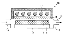
図1は、本実施の形態1で用いられるレジスト表面改質装置10を説明するための概略断面図である。
図1に示すように、処理チャンバ11の保持手段12としてのステージ上に、レジスト膜2が形成された基板1が載置される。ガス供給部15から処理チャンバ11内に酸素を含むガスが供給される。取り扱い容易性とランニングコストとを考慮すると、酸素を含むガスとして大気を用いることができる。大気以外には、Ar等の希ガスと酸素との混合ガスを用いることができる。この混合ガスを用いる場合には、酸素分圧を例えば35%程度に高めることができるため、大気を用いる場合よりも高いレジスト表面改質効率が達成できる。処理チャンバ11内のガスは排気部16から排気される。
First, the semiconductor manufacturing apparatus used in the first embodiment of the present invention will be described.
FIG. 1 is a schematic cross-sectional view for explaining a resist
As shown in FIG. 1, a
処理チャンバ11の上部、すなわちレジスト膜2上方には、真空紫外光を発するランプ13がウィンドウ板14を介して配置されている。すなわち、処理チャンバ11上にランプユニットが配置され、その境界部分にはランプ光が透過可能なようにウィンドウ板14が配置されている。これにより、基板1上のレジスト膜2に対して真空紫外光の照射を行うことができる。ランプ13としては、172nmよりも短波長の光を発するものが好ましい。これは、ランプ光によりレジスト膜2がバルクとして感光すると転写特性に影響が出るためであり、極短波長の光によりレジストの極表層のみ化学変化を起こさせるためである。
A
ランプ13の具体例としては、エネルギ効率を考慮すると、ピーク波長172nmのXe2エキシマランプ、ピーク波長146nmのKr2エキシマランプ、ピーク波長126nmのAr2エキシマランプを用いることができる。波長が短いほど、レジストでの光吸収が大きくなり、化学反応がレジスト表層のみに留まる。よって、レジストバルクとしての感光を抑制することができ、転写特性に影響を与えない。一方、短波長になるほどランプ照度が低下してしまうため、Kr2エキシマランプが最も好適である。
As specific examples of the
なお、F2エキシマレーザは、十分な照度が得られるものの、装置が複雑かつ高コストである。これに対して、エキシマランプは、安価かつコンパクトである。よって、エキシマランプを有するレジスト表面改質装置が、後述する実施の形態4で説明するインライン化に適している。 Incidentally, F 2 excimer laser, although sufficient illuminance is obtained, the device is complex and expensive. On the other hand, the excimer lamp is inexpensive and compact. Therefore, a resist surface modification apparatus having an excimer lamp is suitable for in-line explained in the fourth embodiment described later.
ウィンドウ板14は、ランプ光を透過する材料で形成されたものを用いることができ、具体的にはフッ化カルシウム板を用いることができる。
The
エキシマランプ光はレジスト膜2表層を活性化させると共に、処理チャンバ11内の酸素と反応して活性酸素とオゾンを発生させる。この活性酸素とオゾン、特に活性酸素は効率的にレジスト膜2の表層を酸化させ、親水性に変える。エキシマランプ光がレジスト膜2の表面に照射されると、その酸化効率がより高まり、レジスト膜2表層の親水性化時間を短縮することができる。実際の親水性化処理時間は60secであり、インライン化に適しているかが分かった。
The excimer lamp light activates the surface layer of the resist
なお、上記表面改質装置では、ランプ光をレジスト膜2に照射しているが、ランプ光をレジスト膜2に照射せずに活性酸素及びオゾン発生用にのみ用いてもよい。すなわち、ランプ光を酸素と反応させて活性酸素及びオゾンを発生させ、該発生した活性酸素及びオゾンを処理チャンバに導入する構成としてもよい。これにより、基板1近傍に活性酸素及びオゾンが供給される。この場合、ランプ光をレジスト膜2に照射する場合と比較して親水性化効率は低くなるが、レジスト膜2表層を親水性化するという目的は達成し得る。また、ランプ光がレジスト膜をバルクとして感光することがないため、転写特性に影響が出ることがなく、172nmよりも長波長の光源を用いることができる。
In the surface modifying apparatus, the resist
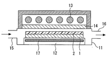
図2は、本実施の形態1で用いられるレジスト表面改質装置の変形例を説明するための概略断面図である。
本変形例では、基板1を載置するステージ12内に、加熱機構17としてのヒータが設けられている。その他の構成は、図1に示したレジスト表面改質装置と同様である。
ランプ13からレジスト膜2にランプ光を照射する際に、図示しない電源からヒータ17に電力供給され、該ヒータ17により基板1を加熱する。これにより、レジスト膜2表層を更に活性化させることができ、親水性化効率を更に高めることができる。
FIG. 2 is a schematic cross-sectional view for explaining a modification of the resist surface modifying apparatus used in the first embodiment.
In this modification, a heater as the
When irradiating the resist
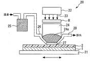
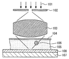
図3は、本実施の形態1で用いられる液浸露光装置20を説明するための概略断面図である。
図3に示すように、2次元的に移動可能なステージ21上に基板1が載置されている。基板1上にはレジスト膜2が形成されている。投影レンズ24とレジスト膜2との隙間には、浸液27が局所的に満たされている。この浸液27は、脱気装置25を通して気泡を取り除いた後、液浸液供給ノズル26から上記隙間に供給される。該供給された浸液27は、所定時間経過後、排水管28を通して排水されて廃液となる。投影レンズ24aとレジスト膜2との隙間は、1mm〜2mm程度である。浸液27としては、例えば、純水を用いることができる。純水は、ArFエキシマレーザ光(波長193nm)を透過し、レジストとの相互作用も少ない。
FIG. 3 is a schematic cross-sectional view for explaining the
As shown in FIG. 3, the
図示しない光源から発せられた露光光23は、照明系22を通過した後、パターンが描画されたレチクルRを透過する。レチクルRを透過した光は、投影系24の投影レンズ24aを介し、さらに浸液27を介してレジスト膜2に対して照射される。露光光23の光源としては、波長193nmのArFエキシマレーザを用いることができる。
The
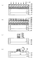
図4は、本実施の形態1による半導体装置の製造方法、より詳細には、微細パターンの形成方法を説明するための工程断面図である。
先ず、図4(a)に示すように、シリコン基板等の基板1上に被加工膜3を形成し、その上にレジスト膜2を形成する。ここで、被加工膜3は、例えば、ゲート電極材料である導電膜としてのドープトポリシリコン膜である。なお、SiO2膜のような絶縁膜等が被加工膜3であってもよい。また、被加工膜3の代わりにシリコン基板自体を被加工基板として加工してもよい。
FIG. 4 is a process cross-sectional view for explaining the semiconductor device manufacturing method according to the first embodiment, more specifically, a fine pattern forming method.
First, as shown in FIG. 4A, a film to be processed 3 is formed on a
次に、図4(b)に示すように、上記レジスト表面改質装置(図1,2参照)を用いて、ランプ光4をレジスト膜2に照射しつつ、基板1を活性酸素雰囲気に曝す。これにより、レジスト膜2の表層が親水性化され、レジスト膜2の濡れ性が改善される。すなわち、レジスト膜2の表層が酸化され、酸化層5が形成される。
Next, as shown in FIG. 4B, the
次に、図4(c)に示すように、上記液浸露光装置(図3参照)を用いて液浸露光法によりパターン露光を行う。レチクルRを透過した露光光23としてのArFエキシマレーザ光は、投影レンズと浸液27とを透過した後、レジスト膜2に照射される。このとき、レジスト膜2表面には親水性の酸化層5が形成されているため、レジスト界面の浸液27におけるマイクロバブルの発生を防止することができる。また、酸化層5は極薄であるため、レジスト膜バルクに対して露光光の遮断、屈折、回折等の影響を与えない。このため、酸化層5は転写性能に悪影響を及ぼさない。
本発明者は、ウェハステージを500mm/secでスキャンしながら露光を行ったところ、マイクロバブルの発生は見られず、マイクロバブル起因の転写不良の発生がないことを確認した。一方、レジスト表面改質処理を行っていない基板に対しても同様の露光を行ったところ、1ロット(25枚)のうちの数枚の基板にマイクロバブル起因の転写不良が発生し、歩留まりを5%低下させていた。
なお、浸液27は脱気装置(25)により脱気した後、レンズ24aとレジスト膜2との隙間に供給されるため、レジスト界面以外での浸液27におけるマイクロバブルの発生を防止することができる。
Next, as shown in FIG. 4C, pattern exposure is performed by an immersion exposure method using the immersion exposure apparatus (see FIG. 3). The ArF excimer laser light as the
The present inventor performed exposure while scanning the wafer stage at 500 mm / sec. As a result, the generation of microbubbles was not observed, and it was confirmed that there was no transfer failure due to the microbubbles. On the other hand, when the same exposure was performed on the substrate not subjected to the resist surface modification treatment, transfer defects due to microbubbles occurred on several substrates in one lot (25 substrates), and the yield was reduced. It was reduced by 5%.
Since the
次に、現像処理を行うと、図4(d)に示すように、レジストパターン2a,5aが形成される。そして、図4(e)に示すように、レジストパターン2a,5aをマスクとして被加工膜3をエッチングすることにより、被加工膜のパターン3aが形成される。最後に、レジストパターン2a,5aを除去すると、図4(f)に示すように、基板1上に微細パターン3aが得られる。
Next, when development processing is performed, resist
以上説明したように、本実施の形態1では、レジスト膜2の表層部分を酸化することにより該表層部分の親水性を高めた後、液浸露光を行うこととした。これにより、液浸露光時に、レジスト界面の浸液27におけるマイクロバブルの発生を防止することができる。よって、レジスト界面のマイクロバブルに起因する転写欠陥の発生を防止することができる。従って、半導体装置の歩留まりを向上させることができる。
As described above, in the first embodiment, the surface layer portion of the resist
なお、本実施の形態1では、レジスト表面改質処理として、活性酸素処理、或いは、活性酸素処理に真空紫外光照射を併用する処理について説明したが、これらの処理に代えてプラズマ酸化を用いることができる。すなわち、酸素分圧下でプラズマを生成し、レジスト膜の極表層部のみを酸化する方法を用いることができる。この方法は既存の酸素プラズマ処理装置を用いることができるため、新規に装置の設計を行う必要がない(後述する実施の形態2,3,4についても同様)。 In the first embodiment, as the resist surface modification treatment, active oxygen treatment or treatment using vacuum ultraviolet light irradiation in combination with active oxygen treatment has been described. However, plasma oxidation is used instead of these treatments. Can do. That is, a method of generating plasma under an oxygen partial pressure and oxidizing only the extreme surface layer portion of the resist film can be used. Since this method can use an existing oxygen plasma processing apparatus, it is not necessary to newly design the apparatus (the same applies to Embodiments 2, 3, and 4 described later).
レジスト膜の濡れ性を改善することによりマイクロバブル(気泡)の発生を防止する方法としては、上述した本実施の形態1による方法の他にも、レジストの構成成分を親水性化する方法や、浸液にアルコールなどの界面活性剤を添加する方法が考えられる。本発明者は、これらの方法についても検討した。その結果を以下に述べる。
レジストの構成成分を親水性化する方法としては、例えば、酸発生剤(PAG:photoacid generator)を親水性のものに替える方法が考えられる。しかしながら、この方法では、親水性の分子が選択的に浸液に遊離(溶解)してしまうため、レジストの成分のバランスが崩れ、転写性能に悪影響が出てしまう。特に、レジスト上面で親水性成分の遊離が起こるため、レジストの膜厚方向でレジスト成分のバランスが崩れてしまい、レジスト上面部が丸まってしまう問題や、T−top形状に繋がってしまうという問題があった。また、浸液に遊離したレジスト成分が投影レンズのコンタミネーションの原因になるという問題もあった。遊離した成分は微量であるが、この成分に露光光の光エネルギーが加わると、投影レンズのコンタミネーションに繋がることが分かった。
また、浸液に界面活性剤を添加する方法も、レンズコンタミネーションの問題があり、露光装置を長時間使用したときのメンテナンスに問題が生じた。また、この方法では、浸液によるレジストダメージの問題もあった。
As a method for preventing the generation of microbubbles (bubbles) by improving the wettability of the resist film, in addition to the method according to the first embodiment described above, a method of making the resist constituents hydrophilic, A method of adding a surfactant such as alcohol to the immersion liquid is conceivable. The inventor also examined these methods. The results are described below.
As a method for making the resist constituents hydrophilic, for example, a method of replacing an acid generator (PAG: photoacid generator) with a hydrophilic one can be considered. However, in this method, hydrophilic molecules are selectively released (dissolved) in the immersion liquid, so that the balance of resist components is lost and transfer performance is adversely affected. In particular, since the hydrophilic component is liberated on the resist upper surface, the balance of the resist component is lost in the resist film thickness direction, and the upper surface of the resist is rounded and the T-top shape is caused. there were. There is also a problem that the resist component released in the immersion liquid causes contamination of the projection lens. Although the amount of the released component is very small, it has been found that if the light energy of the exposure light is added to this component, it leads to contamination of the projection lens.
Also, the method of adding a surfactant to the immersion liquid has a problem of lens contamination, which causes a problem in maintenance when the exposure apparatus is used for a long time. This method also has a problem of resist damage due to immersion liquid.
これに対して、本発明では、上述したように、レジスト表層部におけるレジストポリマの一部をOH化するものであり、レジスト成分の浸液への遊離はほとんどない。このため、レジストバルク部には影響しないため、転写特性に与える影響は無視できるほど小さい。 In contrast, in the present invention, as described above, a part of the resist polymer in the resist surface layer portion is OHated, and the resist component is hardly released into the immersion liquid. For this reason, since the resist bulk portion is not affected, the influence on the transfer characteristics is negligibly small.
実施の形態2.
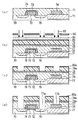
図5は、本実施の形態2による半導体装置の製造方法、より詳細には、MOSトランジスタの形成方法を説明するための工程断面図である。
先ず、図5(a)に示すように、シリコン基板51内にSTI法を用いて素子分離52を形成し、該素子分離52により分離された活性領域に不純物を注入することによりウェル領域53を形成する。そして、シリコン基板51上にゲート絶縁膜54を形成する。ゲート絶縁膜54としては、例えば、シリコン酸化膜、シリコン窒化膜、シリコン酸窒化膜のほか、いわゆる高誘電率膜を用いることができる。
次に、ゲート絶縁膜54上にゲート電極となる導電膜55として、ドープトポリシリコン膜(以下「ポリシリコン膜」と略す。)を形成する。ポリシリコン膜に代えて、シリコンゲルマニウム膜を導電膜55として用いることができる。そして、ポリシリコン膜55上にレジスト膜56を形成する。
続いて、実施の形態1で説明したレジスト表面改質装置(図1,2参照)を用いて、Kr2エキシマランプ光57をレジスト膜56に照射しつつ、基板51を活性酸素雰囲気に曝す。これにより、レジスト膜56の表層が親水性化され、レジスト膜56の濡れ性が改善される。すなわち、レジスト膜56の表層が酸化され、酸化層58が形成される。
FIG. 5 is a process sectional view for explaining the method for manufacturing a semiconductor device according to the second embodiment, more specifically, a method for forming a MOS transistor.
First, as shown in FIG. 5A, an
Next, a doped polysilicon film (hereinafter abbreviated as “polysilicon film”) is formed as a
Subsequently, the
次に、図5(b)に示すように、実施の形態1で説明した液浸露光装置(図3参照)を用いて、液浸露光法によりパターン露光を行う。レチクル(マスク)を透過した露光光60としてのArFエキシマレーザ光は、投影レンズと浸液59とを透過した後、レジスト膜56に照射される。このとき、レジスト膜56表面には酸化層58が形成されているため、レジスト界面の浸液59におけるマイクロバブルの発生を防止することができる。
Next, as shown in FIG. 5B, pattern exposure is performed by an immersion exposure method using the immersion exposure apparatus (see FIG. 3) described in the first embodiment. The ArF excimer laser light as the
次に、現像処理を行うと、レジストパターン56a,58aが形成される。そして、このレジストパターン56a,58aをマスクとしてポリシリコン膜55及びゲート絶縁膜54をドライエッチングする。これにより、図5(c)に示すように、ポリシリコンゲート電極55aが形成される。
Next, when development processing is performed, resist
次に、レジストパターン56a,58aを除去する。そして、図5(d)に示すように、ゲート電極55aをマスクとして低濃度の不純物を基板51内に注入することにより、基板51上層にチャネル領域を挟むエクステンション領域61が形成される。続いて、基板51全面にシリコン窒化膜等の絶縁膜を形成し、該絶縁膜を異方性エッチングすることにより、ゲート電極55a側壁を覆うサイドウォール62を形成する。そして、サイドウォール62及びゲート電極55aをマスクとして高濃度の不純物を基板51内に注入することにより、基板51上層にソース/ドレイン領域63が形成される。
Next, the resist
以上説明したように、本実施の形態2では、レジスト膜56の表層部分を酸化することにより親水性を高めた後、液浸露光を行うこととした。これにより、液浸露光時に、レジスト界面の浸液59におけるマイクロバブルの発生を防止することができる。よって、マイクロバブルに起因する転写欠陥の発生を防止することができる。従って、半導体装置の歩留まりを向上させることができる。ここでの転写欠陥はパターン欠けや潰れだけでなく、基準外寸法欠陥も含む。ゲートは寸法管理基準が厳しいので、パターン直上でなくパターン近傍にできたマイクロバブルの影響も受けやすい。このため、本実施の形態2による方法は特に有効である。
As described above, in the second embodiment, the surface layer portion of the resist
実施の形態3.
上述した実施の形態2では、本発明をMOSFETのゲート電極の形成に適用した例について説明したが、本実施の形態3では、図6〜図10を参照して、本発明を孔パターンの形成に適用した例について説明する。
In the above-described second embodiment, the example in which the present invention is applied to the formation of the gate electrode of the MOSFET has been described. However, in the third embodiment, the present invention is formed by forming a hole pattern with reference to FIGS. An example applied to is described.
図6は、本実施の形態3による半導体装置の製造方法、より詳細には素子要部における孔パターンの形成方法を説明するための工程断面図である。
先ず、図6(a)に示すように、LDD構造を有するMOSFETを形成する。詳細には、シリコン基板70にSTI(shallow trench isolation)法を用いて絶縁膜からなる素子分離71を形成した後、所望のウェル領域を形成し、シリコン基板70上にゲート絶縁膜72を形成する。ゲート絶縁膜72上にゲート電極73を形成すると共に、素子分離71上に配線74を形成する。ゲート電極73及び配線74は、ポリシリコン膜、ポリシリコンゲルマニウム膜、金属のような導電体からなる。ゲート電極73の側壁を覆うサイドウォールスペーサ75を形成する。シリコン基板70上層には、ゲート電極73に対して自己整合的なエクステンション領域と、サイドウォールスペーサ75に対して自己整合的なソース/ドレイン領域とからなる不純物拡散層76を形成する。
そして、上記MOSFETを覆うように、基板全面に絶縁膜77を形成する。本実施の形態3では、この絶縁膜77の所望の位置に孔を形成する方法について説明する。
FIG. 6 is a process cross-sectional view for explaining a method for manufacturing a semiconductor device according to the third embodiment, more specifically, a method for forming a hole pattern in the main part of the element.
First, as shown in FIG. 6A, a MOSFET having an LDD structure is formed. More specifically, an
Then, an insulating
次に、図6(b)に示すように、絶縁膜77上に反射防止膜78を形成し、反射防止膜78上にレジスト膜79を形成する。なお、絶縁膜77が露光光を吸収する材料であれば、反射防止膜78の形成を省略することも可能である。反射防止膜78としては、塗布形式の有機膜を用いることができ、無機材料系のシリコン酸窒化膜やカーボン膜を用いることもできる。
次に、レジスト膜79に対して、実施の形態1で説明した酸素表面処理を施す。これにより、レジスト膜79の表面に酸化層80が形成され、レジスト膜79の表面が親水性化される。すなわち、レジスト膜79の表面の濡れ性が高くなる。例えば、酸素表面処理の時間を60secとすることで、表面から数nmの深さまで十分な親水性層が形成することができる。
そして、所望の孔パターンを有するマスク82を用いて、液浸露光法によりパターン露光を行う。マスク82を通過した露光光83としてのArFエキシマレーザ光は、投影レンズ(図示せず)と浸液81とを透過した後、レジスト膜79に照射される。
Next, as shown in FIG. 6B, an
Next, the oxygen surface treatment described in
Then, pattern exposure is performed by an immersion exposure method using a
次に、現像処理を行うことにより、図6(c)に示すように、開孔を有するレジストパターン(すなわち、孔形状のレジストパターン)80a,79aが形成される。
その後、レジストパターン80a,79aをマスクとして、反射防止膜78及び絶縁膜77をエッチングする。これにより、図6(d)に示すように、絶縁膜77内に所望の孔形状77a,77bが開孔する。その後、レジストパターン80a,79aと反射防止膜78とを除去する。
Next, by performing development processing, as shown in FIG. 6C, resist
Thereafter, the
本実施の形態3では、開口不良の無い微細孔開口77a,77bを絶縁膜77に形成することができる。なお、本実施の形態3では、レジストパターン80a,79aを直接マスクとして絶縁膜をエッチングしたが、例えばポリシリコン膜からなるハードマスクを間接的なマスクとして絶縁膜をエッチングすることができる。すなわち、レジストパターンを一旦ハードマスクにエッチング転写し、レジストパターンを除去し、ハードマスクパターンをマスクとして絶縁膜77をエッチングすることができる。
In the third embodiment, the
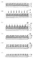
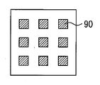
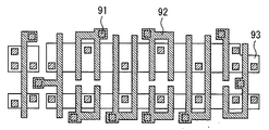
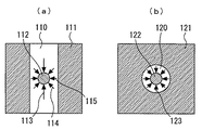
一方、本発明のレジスト表面処理を行わなかった場合は開口不良が多発することが分かった。図7は、等幅/等ピッチで孔90がマトリックス状に並んだ最密集の孔パターン開口のレイアウトの一例を示した上面図である。図8は、ロジック回路の孔パターンのレイアウトの一例を示す上面図である。図8において、符号91は孔、92はゲート配線、93は拡散領域(アクティブエリア)を示している。図7に示すような最密集レイアウトの場合でもパターン開口密度は25%であり、図8に示すようなロジック回路では開口密度は5%以下と小さい。しかしながら、このような開口密度が小さい場合でも、本発明のレジスト表面処理を行わなかった場合は開口不良が多発した。
この原因を検討したところ、以下に示す2つの要因が主要因であることが分かった。
先ず、第1の要因を説明する。図9は、液浸露光時のマイクロバブルの発生状態を示す概略断面図である。図9に示すように、露光光101が所望の孔開口を有するマスク102を通り、投影レンズ103、レンズ保護カバーガラス104、浸液105を介して基板107上に形成されたレジスト膜108に結像照射される。脱気した浸液105を用いてもレジスト膜108表面の濡れ性が低い場合には、スキャン移動の際等に、浸液105中にマイクロバブル106が発生する。発生したバブル106の一部はレジスト膜108/浸液105の界面から遊離し、浸液105中に浮遊する。このマイクロバブル106は、形成する孔パターンの直前になくても、露光光の一部を遮るために転写欠陥を生じやすい。従って、開口密度が低くても転写欠陥が発生しやすい。
On the other hand, it was found that when the resist surface treatment of the present invention was not performed, defective openings frequently occurred. FIG. 7 is a top view showing an example of the layout of the close-packed hole pattern openings in which the
When this cause was examined, it was found that the following two factors were the main factors.
First, the first factor will be described. FIG. 9 is a schematic cross-sectional view showing a state where microbubbles are generated during immersion exposure. As shown in FIG. 9, exposure light 101 passes through a
次に、第2の要因を説明する。図10は、現像工程におけるレジストの現像溶解を示す概略上面図である。図10(a)はライン&スペースパターンのスペースパターン(溝パターン)を現像する場合を示す図であり、図10(b)は孔パターンを現像する場合を示す図である。図10(a),(b)において、符号110,120は開口部を示し、符号111,121はレジスト部を示している。この開口部110,120、すなわちポジ型レジストを用いた場合の露光部に、マイクロバブルの陰112,122がかかる場合について考察する。光露光では回折の影響を受け、一般に露光パターンの中心部の露光強度が強く、中心部から周辺に行くほど露光強度は弱くなる。現像時のレジスト溶解速度は露光強度に応じて変わり、露光強度が強いほど溶解速度は速い。このため、図10(a)に示すように、符号113で示す方向からの現像溶解は急激に進み、符号114、115で示す方向からの現像溶解は溶解が進まなくなる。図10(a)に示すスペースパターンを現像する場合、溶解速度の速い2方向からの浸食を受けるため、マイクロバブルの陰112に起因する転写欠陥は残りにくい。一方、図10(b)に示す孔パターンの場合、溶解速度は符号123で示す何れの方向からも均一であり遅いため、マイクロバブルの陰122に起因する転写欠陥が発生しやすい。この現像液による浸食のされ易さの違いが、第2の要因となっている。
従って、本発明は、孔パターン形成時の転写欠陥の発生の防止に特に有効である。
Next, the second factor will be described. FIG. 10 is a schematic top view showing development and dissolution of the resist in the development process. FIG. 10A is a diagram showing a case where a space pattern (groove pattern) of a line & space pattern is developed, and FIG. 10B is a diagram showing a case where a hole pattern is developed. 10A and 10B,
Therefore, the present invention is particularly effective for preventing the occurrence of transfer defects when forming a hole pattern.
実施の形態4.
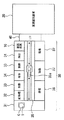
図11は、本発明の実施の形態4による露光システムを説明するための概略図である。
図11に示すように、露光システムは、レジスト塗布現像部30と、図3に示した液浸露光装置20と、両装置20,30間を繋ぐインターフェイス40とを備えている。
FIG. 11 is a schematic diagram for explaining an exposure system according to the fourth embodiment of the present invention.
As shown in FIG. 11, the exposure system includes a resist coating and developing
レジスト塗布現像部30は、複数枚の基板1を収納したウェハキャリアCを載置し、このキャリアCに対して基板1のロード/アンロードを行うローダ/アンローダ31と、レジストの密着性を強化するための前処理を行う前処理ユニット32と、基板の加熱処理を行う加熱ユニット33と、加熱された基板の冷却処理を行う冷却ユニット34と、実施の形態1で説明した表面改質ユニット10と、搬送アーム35aを有し、各ユニット間の基板搬送を行う搬送ユニット35と、前処理が施された基板にレジストを回転塗布する塗布ユニット36と、露光後の現像処理を行う現像ユニット37とを備えている。
The resist coating / developing
次に、上記露光システムの動作について説明する。
先ず、複数の基板1を収納したウェハキャリアCをローダ/アンローダ31に載置する。次に、搬送ユニット35の搬送アーム35aによりキャリアC内の基板1を前処理ユニット32に搬送する。そして、前処理ユニット32において、基板1を加熱し、該加熱した基板1をヘキサメチルジシラザン蒸気に接触させる。これにより、基板1表面が疎水性化され、基板と後に塗布されるレジストとの密着性を向上させることができる。なお、図示しないが、前処理ユニット32は2段構成になっており、それぞれ60secのタクトで疎水性化処理が行われる。
Next, the operation of the exposure system will be described.
First, the wafer carrier C storing a plurality of
次に、疎水性化処理が施された基板1を搬送アーム35aによりレジスト塗布ユニット36に搬送する。そして、レジスト塗布ユニット36において、基板1上にレジスト材料を回転塗布することにより、基板1上にレジスト膜を形成する。なお、図示しないが、レジスト塗布ユニット36は2台構成になっており、それぞれ60secのタクトでレジスト塗布処理が行われる。
Next, the
続いて、レジストが塗布された基板1を搬送アーム35aにより加熱ユニット33に搬送する。そして、加熱ユニット33において露光前ベーク(プリベーク)を行った後、基板1を搬送アーム35aにより冷却ユニット34に搬送して、冷却ユニット34において基板温度が常温になるまで冷却する。
Subsequently, the
その後、冷却された基板1を搬送アーム35aによりレジスト表面改質装置10に搬送し、レジスト表面改質装置10においてレジスト膜表層を酸化することによりレジスト膜表層を親水性化する。この親水性化処理により、レジスト膜の純水に対する接触角が70度から0度に変わる。なお、図示しないが、レジスト表面改質装置10は2段構成になっており、それぞれ60secのタクトで親水性化処理が行われる。
Thereafter, the cooled
次に、レジスト膜表層に親水性化処理が施された基板1をインターフェイス40を通じて液浸露光装置20に搬送する。そして、液浸露光装置20において、液浸露光法を用いたパターン露光を行う。すなわち、投影レンズとレジスト膜との隙間を浸液である純水で満たした後、該浸液を介してレジスト膜に対して露光光を照射する。ここで、上述したように、レジスト膜の純水に対する接触角は0度であるため、レジスト界面の純水におけるマイクロバブルの発生を防止することができる。よって、精度良く液浸露光を行うことができる。
Next, the
パターン露光後、基板1をインターフェイス40を通じて加熱ユニット33に搬送する。そして、加熱ユニット33において露光後ベーク(ポストベーク)を行った後、基板1を搬送アーム35aにより冷却ユニット34に搬送して、冷却ユニット34において基板温度が常温になるまで冷却する。
After the pattern exposure, the
続いて、冷却された基板1を搬送アーム35aにより現像ユニット37に搬送する。そして、現像ユニット37において現像処理を行うことにより、基板1上にレジストパターンが形成される。なお、図示しないが、現像ユニット37は4台構成になっており、それぞれ120secのタクトで現像処理が行われる。現像処理後、基板1を搬送アーム35aによりローダ/アンローダ31に載置されたキャリアC内に戻す。
Subsequently, the cooled
以上説明したように、本実施の形態4では、レジスト表面改質装置10においてレジスト膜の表層部分を酸化することにより該表層部分の親水性を高めた後、液浸露光装置20において液浸露光を行うようにしたため、実施の形態1,2,3と同様に、レジスト界面での浸液におけるマイクロバブルの発生を防止することができ、該マイクロバブル起因の転写欠陥の発生を防止することができる。さらに、本実施の形態4のようにレジスト表面改質装置10と液浸露光装置20をインライン化することにより、マイクロバブル起因の転写欠陥のない微細レジストパターンを120枚/Hrのスループットで形成することができる。
As described above, in the fourth embodiment, the resist
1 基板(シリコン基板)、 2 レジスト膜、 2a 酸化層、 3 被加工膜、 4 真空紫外光(Kr2エキシマランプ光)、 10 レジスト表面改質装置、 11 処理チャンバ、 12 ステージ、 13 ランプ(Kr2エキシマランプ)、 14 ウィンドウ板、 15 ガス供給部、 16 排気部、 17 加熱機構(ヒータ)、 20 液浸露光装置、 21 ステージ、 22 照明系、 23 露光光、 24 投影系、 24a レンズ、 25 脱気装置、 26 供給ノズル、 27 浸液、 28 排水管、 30 レジスト塗布現像部、 31 ローダ/アンローダ、 32 前処理ユニット、 33 加熱ユニット、 34 冷却ユニット、 35 搬送ユニット、 35a 搬送アーム、 36 塗布ユニット、 37 現像ユニット、 40 インターフェイス、 51 基板、 52 素子分離、 53 ウェル領域、 54 ゲート絶縁膜、 55 導電膜(ドープトポリシリコン膜)、 55a ゲート電極、 56 レジスト膜、 56a レジストパターン、 57 ランプ光、 58 酸化層、 59 浸液、 60 露光光、 61 エクステンション領域、 62 サイドウォール、 63 ソース/ドレイン領域、70 シリコン基板、 71 素子分離、 72 ゲート絶縁膜、 73 ゲート電極、 74 配線、 75 サイドウォールスペーサ、 76 不純物拡散層、 77 絶縁膜、 78 反射防止膜、 79 レジスト膜、 80 酸化層、 81 浸液、 82 マスク、 83 露光光、 90,91 孔、 92 ゲート配線、 93 拡散領域、 101 露光光、 102 マスク、 103 投影レンズ、 104 レンズ保護カバーガラス、 105 浸液、 106 マイクロバブル、 107 基板、 108 レジスト膜、 110,120 開口部、 111,121 レジスト部、 112,122 マイクロバブルの陰、 113,114,115,123 現像溶解方向。 1 substrate (silicon substrate), 2 resist film, 2a oxide layer, 3 work film, 4 vacuum ultraviolet light (Kr 2 excimer lamp light), 10 resist surface reformer, 11 processing chamber, 12 stage, 13 lamp (Kr) 2 excimer lamp), 14 window plate, 15 gas supply unit, 16 exhaust unit, 17 heating mechanism (heater), 20 immersion exposure apparatus, 21 stage, 22 illumination system, 23 exposure light, 24 projection system, 24a lens, 25 Deaeration device, 26 supply nozzle, 27 immersion liquid, 28 drain pipe, 30 resist coating and developing section, 31 loader / unloader, 32 pretreatment unit, 33 heating unit, 34 cooling unit, 35 transport unit, 35a transport arm, 36 coating Unit, 37 development unit, 40 interface, 51 substrate, 52 elements 53 well region, 54 gate insulating film, 55 conductive film (doped polysilicon film), 55a gate electrode, 56 resist film, 56a resist pattern, 57 lamp light, 58 oxide layer, 59 immersion liquid, 60 exposure light, 61 Extension region, 62 sidewall, 63 source / drain region, 70 silicon substrate, 71 element isolation, 72 gate insulating film, 73 gate electrode, 74 wiring, 75 sidewall spacer, 76 impurity diffusion layer, 77 insulating film, 78 antireflection Film, 79 resist film, 80 oxide layer, 81 immersion liquid, 82 mask, 83 exposure light, 90, 91 hole, 92 gate wiring, 93 diffusion region, 101 exposure light, 102 mask, 103 projection lens, 104 lens protective cover glass , 105 immersion liquid, 106 microbubbles, 107 substrate, 108 resist film, 110, 120 opening, 111, 121 resist portion, 112, 122 shade of microbubble, 113, 114, 115, 123 development and dissolution direction.
Claims (13)
基板上に形成された被加工膜上あるいは被加工基板上にレジスト膜を形成する工程と、
前記レジスト膜の表層を酸化することにより該表層を親水性化する工程と、
前記レジスト膜の表層を親水性化した後、露光装置の投影レンズと前記レジスト膜との間に浸液を満たし、該浸液を介して前記レジスト膜に対してパターンの露光を行う工程と、
前記パターンを露光した後、現像処理を行うことによりレジストパターンを形成する工程と、
前記レジストパターンをマスクとして前記被加工膜あるいは前記被加工基板をエッチングする工程とを含むことを特徴とする電子デバイスの製造方法。 A method of manufacturing an electronic device using an immersion exposure method,
Forming a resist film on a processing film formed on a substrate or a processing substrate;
Making the surface layer hydrophilic by oxidizing the surface layer of the resist film;
A step of making the surface layer of the resist film hydrophilic, filling an immersion liquid between a projection lens of an exposure apparatus and the resist film, and exposing the pattern to the resist film through the immersion liquid;
A step of forming a resist pattern by performing a development process after exposing the pattern;
And a step of etching the film to be processed or the substrate to be processed using the resist pattern as a mask.
基板上にゲート絶縁膜を形成する工程と、
前記ゲート絶縁膜上に、ゲート電極となる導電膜を形成する工程と、
前記導電膜上にレジスト膜を形成する工程と、
前記レジスト膜の表層を酸化することにより該表層を親水性化する工程と、
前記レジスト膜の表層を親水性化した後、露光装置の投影レンズと前記レジスト膜との間に浸液を満たし、該浸液を介して前記レジスト膜に対してパターンの露光を行う工程と、
前記パターンを露光した後、現像処理を行うことによりレジストパターンを形成する工程と、
前記レジストパターンをマスクとして前記導電膜をエッチングすることによりゲート電極を形成する工程と、
前記レジストパターンを除去した後、前記ゲート電極をマスクとして前記基板内に低濃度の不純物を注入することによりエクステンション領域を形成する工程と、
前記ゲート電極の側壁を覆うサイドウォールを形成する工程と、
前記ゲート電極及びサイドウォールをマスクとして前記基板内に高濃度の不純物を注入することによりソース/ドレイン領域を形成する工程とを含むことを特徴とする電子デバイスの製造方法。 A method of manufacturing an electronic device using an immersion exposure method,
Forming a gate insulating film on the substrate;
Forming a conductive film to be a gate electrode on the gate insulating film;
Forming a resist film on the conductive film;
Making the surface layer hydrophilic by oxidizing the surface layer of the resist film;
A step of making the surface layer of the resist film hydrophilic, filling an immersion liquid between a projection lens of an exposure apparatus and the resist film, and exposing the pattern to the resist film through the immersion liquid;
A step of forming a resist pattern by performing a development process after exposing the pattern;
Forming a gate electrode by etching the conductive film using the resist pattern as a mask;
Forming an extension region by implanting low-concentration impurities into the substrate using the gate electrode as a mask after removing the resist pattern;
Forming a sidewall covering the side wall of the gate electrode;
Forming a source / drain region by injecting a high concentration impurity into the substrate using the gate electrode and the sidewall as a mask.
基板上に被加工膜となる絶縁膜を形成する工程と、
前記絶縁膜の上方にレジスト膜を形成する工程と、
前記レジスト膜の表層を酸化することにより該表層を親水性化する工程と、
前記レジスト膜の表層を親水性化した後、露光装置の投影レンズと前記レジスト膜との間に浸液を満たし、該浸液を介して前記レジスト膜に対して所望の孔パターンの露光を行う工程と、
前記孔パターンを露光した後、現像処理を行うことにより開孔を有するレジストパターンを形成する工程と、
前記レジストパターンを直接あるいは間接のマスクとして前記絶縁膜をエッチングすることにより、前記絶縁膜に孔を形成する工程とを含むことを特徴とする電子デバイスの製造方法。 A method of manufacturing an electronic device using an immersion exposure method,
Forming an insulating film to be processed on the substrate;
Forming a resist film above the insulating film;
Making the surface layer hydrophilic by oxidizing the surface layer of the resist film;
After making the surface layer of the resist film hydrophilic, an immersion liquid is filled between the projection lens of the exposure apparatus and the resist film, and a desired hole pattern is exposed to the resist film through the immersion liquid. Process,
A step of forming a resist pattern having openings by performing a development process after exposing the hole pattern;
Forming a hole in the insulating film by etching the insulating film using the resist pattern as a direct or indirect mask.
前記基板を活性酸素雰囲気に曝すことにより前記レジスト膜の表層を酸化することを特徴とする電子デバイスの製造方法。 In the manufacturing method of the electronic device in any one of Claim 1 to 3,
A method of manufacturing an electronic device, wherein the surface layer of the resist film is oxidized by exposing the substrate to an active oxygen atmosphere.
前記基板を活性酸素雰囲気に曝しながら前記レジスト膜に真空紫外光を照射することにより前記レジスト膜の表層を酸化することを特徴とする電子デバイスの製造方法。 In the manufacturing method of the electronic device in any one of Claim 1 to 4,
A method of manufacturing an electronic device, wherein the surface layer of the resist film is oxidized by irradiating the resist film with vacuum ultraviolet light while exposing the substrate to an active oxygen atmosphere.
酸素に真空紫外光を照射することにより活性酸素を発生させ、該活性酸素を前記基板の周辺に供給することにより前記レジスト膜の表層を酸化することを特徴とする電子デバイスの製造方法。 In the manufacturing method of the electronic device of Claim 4,
A method of manufacturing an electronic device, wherein active oxygen is generated by irradiating oxygen to vacuum ultraviolet light, and the surface layer of the resist film is oxidized by supplying the active oxygen to the periphery of the substrate.
前記基板を酸素プラズマ雰囲気に曝すことにより前記レジスト膜の表層を酸化することを特徴とする電子デバイスの製造方法。 In the manufacturing method of the electronic device in any one of Claim 1 to 3,
A method of manufacturing an electronic device, wherein the surface layer of the resist film is oxidized by exposing the substrate to an oxygen plasma atmosphere.
前記真空紫外光は、波長が172nm以下の光であることを特徴とする電子デバイスの製造方法。 In the manufacturing method of the electronic device according to claim 5,
The method of manufacturing an electronic device, wherein the vacuum ultraviolet light is light having a wavelength of 172 nm or less.
前記真空紫外光は、Kr2エキシマランプ光であることを特徴とする電子デバイスの製造方法。 In the manufacturing method of the electronic device according to claim 5,
The method of manufacturing an electronic device, wherein the vacuum ultraviolet light is Kr 2 excimer lamp light.
基板上にレジスト膜を形成するレジスト塗布装置と、
前記レジスト膜の表層を酸化し、該表層を親水性に改質する表面改質装置と、
投影レンズと前記レジスト膜との間に浸液を満たし、該浸液を介して前記レジスト膜に対してパターンの露光を行う液浸露光装置と、
前記パターンが露光された前記レジスト膜に対して現像処理を行う現像装置とを備えたことを特徴とする露光システム。 An exposure system for forming a resist pattern on a substrate,
A resist coating apparatus for forming a resist film on the substrate;
A surface modification device that oxidizes the surface layer of the resist film and modifies the surface layer to be hydrophilic;
An immersion exposure apparatus that fills an immersion liquid between the projection lens and the resist film, and exposes the pattern to the resist film through the immersion liquid;
An exposure system comprising: a developing device that performs a developing process on the resist film exposed to the pattern.
前記表面改質装置は、処理チャンバと、
前記処理チャンバ内に前記基板を保持する保持手段と、
前記処理チャンバ内に酸素を含有するガスを供給するガス供給部と、
前記酸素と反応し活性酸素を発生させると共に、前記レジスト膜の表層を活性化させる真空紫外光を発するランプとを有することを特徴とする露光システム。 The exposure system according to claim 10, wherein
The surface modification apparatus includes a processing chamber,
Holding means for holding the substrate in the processing chamber;
A gas supply unit for supplying a gas containing oxygen into the processing chamber;
An exposure system comprising: a lamp that reacts with oxygen to generate active oxygen and emits vacuum ultraviolet light that activates a surface layer of the resist film.
前記表面改質装置は、前記レジスト膜に対して活性酸素を供給する活性酸素供給部を有することを特徴とする露光システム。 The exposure system according to claim 10, wherein
The exposure system according to claim 1, wherein the surface modification apparatus includes an active oxygen supply unit that supplies active oxygen to the resist film.
前記表面改質装置は、前記レジスト膜に対して酸素プラズマを用いた処理を行う酸素プラズマ処理装置であることを特徴とする露光システム。 The exposure system according to claim 10, wherein
The exposure system according to claim 1, wherein the surface modification apparatus is an oxygen plasma processing apparatus that performs processing using oxygen plasma on the resist film.
Priority Applications (1)
| Application Number | Priority Date | Filing Date | Title |
|---|---|---|---|
| JP2004296427A JP2006108564A (en) | 2004-10-08 | 2004-10-08 | Electronic device manufacturing method and exposure system |
Applications Claiming Priority (1)
| Application Number | Priority Date | Filing Date | Title |
|---|---|---|---|
| JP2004296427A JP2006108564A (en) | 2004-10-08 | 2004-10-08 | Electronic device manufacturing method and exposure system |
Publications (1)
| Publication Number | Publication Date |
|---|---|
| JP2006108564A true JP2006108564A (en) | 2006-04-20 |
Family
ID=36377897
Family Applications (1)
| Application Number | Title | Priority Date | Filing Date |
|---|---|---|---|
| JP2004296427A Pending JP2006108564A (en) | 2004-10-08 | 2004-10-08 | Electronic device manufacturing method and exposure system |
Country Status (1)
| Country | Link |
|---|---|
| JP (1) | JP2006108564A (en) |
Cited By (8)
| Publication number | Priority date | Publication date | Assignee | Title |
|---|---|---|---|---|
| JP2007081373A (en) * | 2005-09-13 | 2007-03-29 | Taiwan Semiconductor Manufacturing Co Ltd | Immersion lithography method and apparatus |
| JP2008071984A (en) * | 2006-09-15 | 2008-03-27 | Tokyo Electron Ltd | Exposure and development processing methods |
| JP2010211153A (en) * | 2009-03-12 | 2010-09-24 | Renesas Electronics Corp | Resist pattern forming method |
| US7816070B2 (en) | 2006-08-02 | 2010-10-19 | Tdk Corporation | Substrate used for immersion lithography process, method of manufacturing substrate used for immersion lithography process, and immersion lithography |
| JP2012189796A (en) * | 2011-03-10 | 2012-10-04 | Harison Toshiba Lighting Corp | Apparatus for manufacturing liquid crystal panel and method for manufacturing liquid crystal panel |
| EP3093712A1 (en) | 2015-05-14 | 2016-11-16 | Renesas Electronics Corporation | Photolithographic process for manufacturing a semiconductor device |
| US20220004103A1 (en) * | 2018-11-16 | 2022-01-06 | Lam Research Corporation | Bubble defect reduction |
| CN114911141A (en) * | 2022-07-11 | 2022-08-16 | 上海传芯半导体有限公司 | EUV lithography method and EUV lithography apparatus |
-
2004
- 2004-10-08 JP JP2004296427A patent/JP2006108564A/en active Pending
Cited By (15)
| Publication number | Priority date | Publication date | Assignee | Title |
|---|---|---|---|---|
| JP2007081373A (en) * | 2005-09-13 | 2007-03-29 | Taiwan Semiconductor Manufacturing Co Ltd | Immersion lithography method and apparatus |
| US7816070B2 (en) | 2006-08-02 | 2010-10-19 | Tdk Corporation | Substrate used for immersion lithography process, method of manufacturing substrate used for immersion lithography process, and immersion lithography |
| JP2008071984A (en) * | 2006-09-15 | 2008-03-27 | Tokyo Electron Ltd | Exposure and development processing methods |
| JP2010211153A (en) * | 2009-03-12 | 2010-09-24 | Renesas Electronics Corp | Resist pattern forming method |
| JP2012189796A (en) * | 2011-03-10 | 2012-10-04 | Harison Toshiba Lighting Corp | Apparatus for manufacturing liquid crystal panel and method for manufacturing liquid crystal panel |
| KR20160134515A (en) | 2015-05-14 | 2016-11-23 | 르네사스 일렉트로닉스 가부시키가이샤 | Manufacturing method of semiconductor device |
| EP3093712A1 (en) | 2015-05-14 | 2016-11-16 | Renesas Electronics Corporation | Photolithographic process for manufacturing a semiconductor device |
| JP2016218099A (en) * | 2015-05-14 | 2016-12-22 | ルネサスエレクトロニクス株式会社 | Manufacturing method of semiconductor device |
| US9627203B2 (en) | 2015-05-14 | 2017-04-18 | Renesas Electronics Corporation | Manufacturing method of semiconductor device |
| US9847226B2 (en) | 2015-05-14 | 2017-12-19 | Renesas Electronics Corporation | Manufacturing method of semiconductor device |
| US20220004103A1 (en) * | 2018-11-16 | 2022-01-06 | Lam Research Corporation | Bubble defect reduction |
| US12248252B2 (en) * | 2018-11-16 | 2025-03-11 | Lam Research Corporation | Bubble defect reduction |
| CN114911141A (en) * | 2022-07-11 | 2022-08-16 | 上海传芯半导体有限公司 | EUV lithography method and EUV lithography apparatus |
| CN114911141B (en) * | 2022-07-11 | 2022-09-23 | 上海传芯半导体有限公司 | EUV lithography method and EUV lithography apparatus |
| KR102598196B1 (en) * | 2022-07-11 | 2023-11-03 | 상하이 촨신 세미컨덕터 컴퍼니 리미티드 | Euv lithography method and euv lithography apparatus |
Similar Documents
| Publication | Publication Date | Title |
|---|---|---|
| US20050069819A1 (en) | Method for forming resist pattern and method for manufacturing semiconductor device | |
| CN1311522C (en) | Pattern forming method and method of manufacturing semiconductor device | |
| JP5295968B2 (en) | Method and apparatus for manufacturing semiconductor device | |
| TWI699821B (en) | Manufacturing method of semiconductor device | |
| US8268535B2 (en) | Pattern formation method | |
| JP5516931B2 (en) | Resist pattern forming method | |
| JP2010182732A (en) | Method of manufacturing semiconductor device | |
| CN1924706A (en) | Lithography Methods for Semiconductor Manufacturing | |
| JP2006108564A (en) | Electronic device manufacturing method and exposure system | |
| KR100905827B1 (en) | Method for forming hard mask pattern in semiconductor device | |
| KR101024143B1 (en) | Micro pattern formation method | |
| JP2005079226A (en) | Manufacturing method of semiconductor device | |
| JP2025023029A (en) | SUBSTRATE PROCESSING METHOD AND SUBSTRATE PROCESSING APPARATUS | |
| US20090123878A1 (en) | Patterning method | |
| JP2010156819A (en) | Semiconductor device manufacturing method | |
| JP5137333B2 (en) | Method for forming mask pattern for ion implantation and method for manufacturing semiconductor device | |
| US7416990B2 (en) | Method for patterning low dielectric layer of semiconductor device | |
| JP7599562B2 (en) | SUBSTRATE PROCESSING METHOD AND SUBSTRATE PROCESSING SYSTEM | |
| JP2001326173A (en) | Pattern formation method | |
| US20080032437A1 (en) | Exposure method for upper layer of hole of semiconductor device | |
| CN2742470Y (en) | Immersion Lithography System | |
| KR100691934B1 (en) | Contact hole formation method of semiconductor device | |
| CN1624588B (en) | Immersion lithography system, method of illuminating semiconductor structures and manufacturing method | |
| JP4392229B2 (en) | Wiring pattern forming method | |
| CN121844261A (en) | Substrate processing method, substrate processing apparatus and computer storage medium |