JP2006100676A - Semiconductor integrated circuit - Google Patents
Semiconductor integrated circuit Download PDFInfo
- Publication number
- JP2006100676A JP2006100676A JP2004286652A JP2004286652A JP2006100676A JP 2006100676 A JP2006100676 A JP 2006100676A JP 2004286652 A JP2004286652 A JP 2004286652A JP 2004286652 A JP2004286652 A JP 2004286652A JP 2006100676 A JP2006100676 A JP 2006100676A
- Authority
- JP
- Japan
- Prior art keywords
- semiconductor integrated
- integrated circuit
- circuit
- separation
- transmission amplifier
- Prior art date
- Legal status (The legal status is an assumption and is not a legal conclusion. Google has not performed a legal analysis and makes no representation as to the accuracy of the status listed.)
- Granted
Links
Images


Abstract
Description
本発明は、半導体集積回路に関し、より詳細には、同一チップ上に配置された発振器と送信増幅器との相互干渉抑圧を施した半導体集積回路に関する。 The present invention relates to a semiconductor integrated circuit, and more particularly to a semiconductor integrated circuit in which mutual interference suppression between an oscillator and a transmission amplifier arranged on the same chip is performed.
半導体集積回路に発振器を内蔵した場合、他の回路ブロックからのノイズあるいは信号の漏れ込みにより発振器の特性が悪化するという問題がある。特に、発振器が電圧制御発振器のような周波数可変の発振器の場合には、外部からの影響により発振器出力が変調されてしまい、正常な動作を妨げることになる。この問題を解決するための回路ブロック構成として、発振器と後段の増幅器あるいはミキサとの間にバッファアンプを配置して後段からの影響を減らす方法がよくとられている。 When an oscillator is built in a semiconductor integrated circuit, there is a problem that the characteristics of the oscillator deteriorate due to noise or signal leakage from other circuit blocks. In particular, when the oscillator is a variable frequency oscillator such as a voltage controlled oscillator, the output of the oscillator is modulated due to an external influence, and normal operation is hindered. As a circuit block configuration for solving this problem, a method is often used in which a buffer amplifier is arranged between an oscillator and a subsequent amplifier or mixer to reduce the influence from the subsequent stage.
この方法は、信号パスを通って発振器に回り込むノイズあるいは干渉信号を抑圧することを目的としているが、サブストレート(半導体基板)を介しての干渉は抑圧できない。これに対して、信号の出力パッドから基板を介してのノイズ回り込みを低減するものがある(例えば、特許文献1参照)。 This method is intended to suppress noise or interference signals that pass through the signal path to the oscillator, but cannot suppress interference through the substrate (semiconductor substrate). On the other hand, there is one that reduces noise wraparound from a signal output pad through a substrate (for example, see Patent Document 1).
しかし、この半導体集積回路内に発振器および送信増幅器の両方が内蔵されている場合には、この送信増幅器自体からのノイズあるいは干渉信号の発生が大きく、出力パッドだけの影響を減らしただけでは十分な性能を出せないといった問題がある。 However, when both an oscillator and a transmission amplifier are built in this semiconductor integrated circuit, noise or interference signals are generated greatly from the transmission amplifier itself, and it is sufficient to reduce the influence of only the output pad. There is a problem that performance cannot be achieved.
本発明は上述のような課題を解決するためになされたもので、外乱に強い発振器の構成を取ることにより、発振器および送信増幅器を1チップ化した場合にもノイズあるいは干渉信号の影響を抑えた半導体集積回路を得ることを目的としている。 The present invention has been made to solve the above-described problems. By adopting an oscillator configuration that is resistant to disturbances, the influence of noise or interference signals can be suppressed even when the oscillator and the transmission amplifier are integrated into a single chip. The object is to obtain a semiconductor integrated circuit.
本発明に係る半導体集積回路は、発振回路および送信増幅回路が同一チップ上に配置された半導体集積回路において、発振回路は、バラクタダイオード対を有する差動電圧制御発振回路であり、バラクタダイオード対のアノード端子同士もしくはカソード端子同士を近接に配置し、共通の信号線を用いてアノード端子もしくはカソード端子を接続したものである。 A semiconductor integrated circuit according to the present invention is a semiconductor integrated circuit in which an oscillation circuit and a transmission amplifier circuit are arranged on the same chip. The oscillation circuit is a differential voltage controlled oscillation circuit having a varactor diode pair. The anode terminals or the cathode terminals are arranged close to each other, and the anode terminal or the cathode terminal is connected using a common signal line.
本発明によれば、バラクタダイオード対を近接配置して共通の信号線で接続することにより、バラクタダイオード対に入力されるノイズあるいは干渉信号を等しくして差動動作への影響をなくすことができ、発振器および送信増幅器を1チップ化した場合にもノイズあるいは干渉信号の影響を抑えた半導体集積回路を得ることができる。 According to the present invention, by arranging varactor diode pairs in close proximity and connecting them with a common signal line, it is possible to equalize the noise or interference signal input to the varactor diode pairs and eliminate the influence on the differential operation. Even when the oscillator and the transmission amplifier are made into one chip, a semiconductor integrated circuit in which the influence of noise or interference signals is suppressed can be obtained.
実施の形態1.
以下、本発明の半導体集積回路の好適な実施の形態につき図面を用いて説明する。図1は、本発明の実施の形態1における半導体集積回路の一例を示す回路構成図である。この半導体集積回路1は、複数の回路ブロックを集積化したシステムLSIであり、例えば、SiGeBiCMOSあるいはCMOS半導体集積回路製造技術により単結晶シリコンなどからなる1個の半導体チップ上に形成される。
Embodiment 1 FIG.
Hereinafter, preferred embodiments of a semiconductor integrated circuit according to the present invention will be described with reference to the drawings. FIG. 1 is a circuit configuration diagram showing an example of a semiconductor integrated circuit according to Embodiment 1 of the present invention. The semiconductor integrated circuit 1 is a system LSI in which a plurality of circuit blocks are integrated. For example, the semiconductor integrated circuit 1 is formed on a single semiconductor chip made of single crystal silicon or the like by SiGeBiCMOS or CMOS semiconductor integrated circuit manufacturing technology.
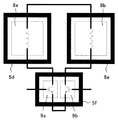
チップ周囲には多数のボンディングパッド2が配置され、各種電源やグランド(GND)、I/Oの機能を有する。このチップ内には、発振回路3および送信増幅回路4が内蔵され、それぞれの回路は、回路間の距離が最も大きくなるように、半導体集積回路1のチップの対角線上の両端に配置されている。送信増幅回路4から出力されるRF信号を取り出すボンディングパッド2aは、送信増幅回路4が配置された対角線上の一端の近くに配置されるため、結果的に発振回路3からも離れることになり、ノイズ等の影響を低減することができる。
A large number of
発振回路3および送信増幅回路4は、PN分離による分離層5a、5bによって、自身以外の回路ブロックとそれぞれ分離される。この際、分離層5a、5bは、図のように各回路ブロックを完全に取り囲む。なお、このような分離層5a、5bは、トレンチにより構成することも可能である。
The
分離層5aは、他の回路ブロックからのノイズ、および干渉信号が発振回路3の内部に入り込むことにより発振周波数が変動することを防ぐことができる。また、分離層5bは、送信増幅回路4から発生するノイズ、および発振回路など他の回路ブロックにとっての干渉信号が漏れ出すのを防ぐことができる。
The
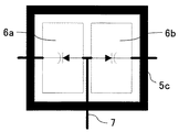
図2は、本発明の実施の形態1における発振回路3に電圧制御発振器を用いた場合の内部回路構成を示した図である。この電圧制御発振器は、差動で動作する2つのバラクタダイオード6a、6bを備えている。バラクタダイオード6a、6bは、可変容量素子であり、このバラクタダイオード6a、6bを用いた電圧制御発振器は、制御電圧を変えることでバラクタダイオード6a、6bの容量の値を変化させ、発信周波数を変化させることができる。図2において、バラクタダイオード6a、6bは、すぐ隣同士に配置され、互いに共通となる信号線7につながるアノード端子がそれぞれ対向するように隣接して置かれている。
FIG. 2 is a diagram showing an internal circuit configuration when a voltage-controlled oscillator is used for
仮に、信号線7につながるバラクタダイオード6a、6bのアノード端子同士が離れていると、この信号線7に干渉信号がのった場合、高周波的にみれば差動で動作する2つのバラクタダイオード6a、6bの端子に入力される干渉信号は、位相差をもったり、あるいは振幅が異なったりする可能性がある。図2の配置は、これらの問題を防ぐために行っており、2つのバラクタダイオード6a、6bへ入力される干渉信号を等しくすることにより、差動動作への影響をなくすことができる。
If the anode terminals of the
図2において、2つのバラクタダイオード6a、6bは、アノード端子が信号線7とつながる共通の端子となっているが、カソード端子を共通とする回路構成においても、同じ方式で配置することにより同様の効果を得ることができる。
In FIG. 2, the two
分離層5cは、差動で動作する2つのバラクタダイオード6a、6bへ基板を介してノイズや干渉信号が入力されるのを防ぐために配置されており、バラクタダイオード6a、6bを完全に囲っている。図2において、2つのバラクタダイオード6a、6bしか分離層内に入っていないが、電圧制御発振器に2つ以上のバラクタダイオードを使用している場合、同じくこの分離層5c内に配置してもよい。
The
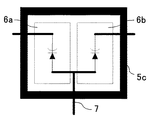
図3は、本発明の実施の形態1における発振回路3に電圧制御発振器を用いた場合の別の内部回路構成を示した図である。図3の電圧制御発振器において、差動で動作するバラクタダイオード6a、6bは、図2と同じく、すぐ隣に配置され、互いに共通となる信号線7につながるアノード端子が隣接するように置かれている。さらに、バラクタダイオード6a、6bは、それぞれが差動で動作した場合の電界を互いに相殺するように、アノード端子およびカソード端子の向きがともに同じになるように配置されている。
FIG. 3 is a diagram showing another internal circuit configuration when a voltage-controlled oscillator is used for
このような配置をとることにより、外部より侵入した干渉信号が2つのバラクタダイオード6a、6bに印加されても、それぞれが差動で動作した場合の電界を互いに相殺することにより、差動動作に与える影響を小さくすることができる。
By adopting such an arrangement, even when an interference signal entering from the outside is applied to the two
なお、図2および図3に示したバラクタダイオード6a、6bの配置法は、図1のような送信増幅回路が同一チップ上に配置された半導体集積回路だけでなく、電圧制御発振回路を含む半導体集積回路全般に適用できる。 2 and 3 is not limited to the semiconductor integrated circuit in which the transmission amplifier circuit as shown in FIG. 1 is arranged on the same chip, but also a semiconductor including a voltage controlled oscillation circuit. Applicable to all integrated circuits.
図4は、本発明の実施の形態1における送信増幅回路4にスパイラルインダクタを用いた場合の内部回路構成を示した図である。図4において、スパイラルインダクタ8a、8bは、増幅器の負荷として使用されている。このスパイラルインダクタ8a、8bは、それぞれ分離層5d、5eにより他の素子と分離される。この分離層5d、5eにより、スパイラルインダクタ8a、8bからサブストレートへ放射されるノイズや干渉信号を抑圧することができる。なお、図4では、差動のスパイラルインダクタ8a、8bをそれぞれ別の分離層5d、5eで囲ってあるが、差動分の2つのスパイラルインダクタ8a、8bをまとめて囲んでもよい。
FIG. 4 is a diagram showing an internal circuit configuration when a spiral inductor is used in transmission amplifier circuit 4 in the first embodiment of the present invention. In FIG. 4,
なお、スパイラルインダクタ8a、8bは、増幅器の負荷として使用されているものだけでなく、ベースフィードなど送信増幅器で使用されているものすべてについて適用できる。
The
トランジスタ9a、9bは、図4の送信増幅器内で増幅素子として使用されているものである。このトランジスタ9a、9bは、差動分まとめて分離層5fで他の回路部分と分離される。ここで、分離層5fは、各トランジスタ9a、9bをそれぞれ別に周囲を囲んでもよい。分離層5fは、各トランジスタ9a、9bから発生するノイズ、および発振回路3など他の回路ブロックにとっての干渉信号が漏れ出すのを防ぐ。
The
なお、図4に示した送信増幅回路内の素子配置法は、図1のような送信増幅回路が同一チップ上に配置された半導体集積回路だけでなく、送信増幅回路を含む半導体集積回路全般に適用できる。 The element arrangement method in the transmission amplifier circuit shown in FIG. 4 is applied not only to the semiconductor integrated circuit in which the transmission amplifier circuit as shown in FIG. 1 is arranged on the same chip, but also to all semiconductor integrated circuits including the transmission amplifier circuit. Applicable.
図5は、本発明の実施の形態1における半導体基板の分離層をPN分離とした場合の断面図である。図5では、分離層によって囲まれる素子10は、受動素子としたが、能動素子の場合も同様である。素子10を分離する分離層は、p+拡散層11とn+拡散層12とで構成される。
FIG. 5 is a cross-sectional view when the separation layer of the semiconductor substrate in the first embodiment of the present invention is PN separation. In FIG. 5, the
p+拡散層11は、接続線13によりDC動作する回路のグランドラインであるDC−GNDに接続されている。また、n+拡散層12は、接続線14によりDC動作する回路の電源ラインであるDC―VCCに接続されている。ここで、DC−GNDは、高周波信号を扱う素子に直接接続されていないグランドラインのことであり、DC―VCCは、高周波信号を扱う素子に直接接続されていない電源ラインのことである。
The p +
このように、PN分離層をそれぞれDC−VCCおよびDC−GNDに接続することで、p+拡散層11とn+拡散層12の電位が振られることがなく、確実なシールド効果を得ることができる。
In this way, by connecting the PN isolation layer to DC-VCC and DC-GND, respectively, the potential of the p +
なお、半導体集積回路が、図1のように発振回路3と送信増幅回路4の両方を内蔵している場合、発振回路3を囲むPN分離層の電源ライン/グランドラインと、送信増幅回路4を囲むPN分離層の電源ライン/グランドラインとはIC内で共通化されていないことが好ましい。
If the semiconductor integrated circuit includes both the
図6は、本発明の実施の形態1における送信増幅回路4の配置方法の一例を示す図である。図6において、送信増幅回路4は、単段の増幅回路15a、15b、15cの縦続接続で構成されている。このような構成の多段増幅回路では、当然増幅回路15aが最も低いRF信号電力を扱い、最終段の増幅回路15cが最も高いRF信号電力を扱う。なお、図6においては、増幅回路は3段から成っているが、何段であっても同様である。
FIG. 6 is a diagram showing an example of an arrangement method of the transmission amplifier circuit 4 in the first embodiment of the present invention. In FIG. 6, the transmission amplifier circuit 4 is constituted by a cascade connection of single-
通常、各段の増幅回路15a、15b、15cへバイアス電圧、バイアス電流を与えるバイアス回路16は、信号の増幅部の近くに配置されるが、ここではバイアス回路16のみを増幅部から分離した構成としている。さらに、送信増幅回路全体を囲む分離層5gの外側に、このバイアス回路16を配置している。また、バイアス回路16は、最も高いRF信号電力を扱う最終段の増幅回路15cが他の増幅回路15a、15bと比較して最も遠くなる位置に配置されている。
Normally, the
このように各段の増幅回路15a、15b、15cを分離層5gで囲むことにより、各トランジスタから発生するノイズを防止するとともに、発振回路3など他の回路ブロックにとっての干渉信号が漏れ出すのを防ぐことができる。また、バイアス回路16の配置を最終段の増幅回路15cから離し、かつ分離層5gの外側とすることで、送信増幅器から漏れ出すノイズや干渉信号により、自身のバイアス回路16が干渉を受けて、特性が悪化することを防ぐことができる。
By surrounding the
なお、図6においては、多段増幅回路全体を分離層で囲んだが、最も高いRF信号電力を扱う最終段の増幅回路のみを分離層で囲むことによっても、同様の効果を得ることができる。 In FIG. 6, the entire multistage amplifier circuit is surrounded by the separation layer, but the same effect can be obtained by surrounding only the final stage amplifier circuit that handles the highest RF signal power with the separation layer.
1 半導体集積回路、2、2a ボンディングパッド、3 発振回路、4 送信増幅回路、5a、5b、5c、5d、5e、5f、5g 分離層、6a、6b バラクタダイオード、7 信号線、8a、8b スパイラルインダクタ、9a、9b トランジスタ、10 素子、11 p+拡散層、12 n+拡散層、13 接続線(グランドライン)、14 接続線(電源ライン)、15a、15b、15c 増幅回路、16 バイアス回路。
DESCRIPTION OF SYMBOLS 1 Semiconductor integrated
Claims (10)
前記発振回路は、バラクタダイオード対を有する差動電圧制御発振回路であり、前記バラクタダイオード対のアノード端子同士もしくはカソード端子同士を近接に配置し、共通の信号線を用いて前記アノード端子もしくは前記カソード端子を接続したことを特徴とする半導体集積回路。 In a semiconductor integrated circuit in which an oscillation circuit and a transmission amplifier circuit are arranged on the same chip,
The oscillation circuit is a differential voltage controlled oscillation circuit having a varactor diode pair, wherein the anode terminals or the cathode terminals of the varactor diode pair are arranged close to each other, and the anode terminal or the cathode is used using a common signal line. A semiconductor integrated circuit characterized by connecting terminals.
前記バラクタダイオード対の前記アノード端子および前記カソード端子の向きがともに同じになるように配置したことを特徴とする半導体集積回路。 The semiconductor integrated circuit according to claim 1,
A semiconductor integrated circuit characterized in that the anode terminal and the cathode terminal of the varactor diode pair are arranged in the same direction.
前記バラクタダイオード対の周囲をPN分離による分離層で囲んだことを特徴とする半導体集積回路。 The semiconductor integrated circuit according to claim 1 or 2,
A semiconductor integrated circuit characterized in that the varactor diode pair is surrounded by a separation layer by PN separation.
前記発振回路の周囲をPN分離による分離層で囲んだことを特徴とする半導体集積回路。 The semiconductor integrated circuit according to any one of claims 1 to 3,
A semiconductor integrated circuit, wherein the oscillation circuit is surrounded by a separation layer by PN separation.
前記送信増幅回路は、スパイラルインダクタを有する差動増幅回路であり、前記スパイラルインダクタの周囲をPN分離による分離層で囲んだことを特徴とする半導体集積回路。 The semiconductor integrated circuit according to any one of claims 1 to 4,
The transmission amplifier circuit is a differential amplifier circuit having a spiral inductor, and the spiral inductor is surrounded by a separation layer by PN separation.
前記送信増幅回路は、多段増幅回路であり、前記多段増幅回路を構成する増幅用トランジスタのうち少なくとも最終段を構成する増幅用トランジスタ部をPN分離による分離層で囲んだことを特徴とする半導体集積回路。 The semiconductor integrated circuit according to any one of claims 1 to 4,
The transmission amplifier circuit is a multistage amplifier circuit, and a semiconductor integrated circuit characterized in that at least an amplification transistor part constituting the final stage among the amplification transistors constituting the multistage amplifier circuit is surrounded by a separation layer by PN separation circuit.
前記送信増幅回路の周囲をPN分離による分離層で囲んだことを特徴とする半導体集積回路。 The semiconductor integrated circuit according to claim 5 or 6,
A semiconductor integrated circuit characterized in that the transmission amplifier circuit is surrounded by a separation layer by PN separation.
前記PN分離に使用したp+拡散層をDC動作する回路のグランドラインへ接続し、n+拡散層をDC動作する回路の電源ラインへ接続したことを特徴とする半導体集積回路。 The semiconductor integrated circuit according to any one of claims 3 to 7,
A semiconductor integrated circuit, wherein the p + diffusion layer used for the PN separation is connected to a ground line of a circuit that operates DC, and the n + diffusion layer is connected to a power supply line of a circuit that operates DC.
前記送信増幅回路を構成するバイアス回路部を、前記PN分離による分離層の外側に配置したことを特徴とする半導体集積回路。 The semiconductor integrated circuit according to any one of claims 3 to 8,
A semiconductor integrated circuit, wherein a bias circuit section constituting the transmission amplifier circuit is arranged outside a separation layer by the PN separation.
前記発振回路と前記送信増幅回路は、前記チップ上の対角線の両端位置に配置されたことを特徴とする半導体集積回路。 The semiconductor integrated circuit according to any one of claims 1 to 9,
The semiconductor integrated circuit according to claim 1, wherein the oscillation circuit and the transmission amplifier circuit are disposed at opposite end positions of a diagonal line on the chip.
Priority Applications (1)
| Application Number | Priority Date | Filing Date | Title |
|---|---|---|---|
| JP2004286652A JP4932147B2 (en) | 2004-09-30 | 2004-09-30 | Semiconductor integrated circuit |
Applications Claiming Priority (1)
| Application Number | Priority Date | Filing Date | Title |
|---|---|---|---|
| JP2004286652A JP4932147B2 (en) | 2004-09-30 | 2004-09-30 | Semiconductor integrated circuit |
Publications (2)
| Publication Number | Publication Date |
|---|---|
| JP2006100676A true JP2006100676A (en) | 2006-04-13 |
| JP4932147B2 JP4932147B2 (en) | 2012-05-16 |
Family
ID=36240169
Family Applications (1)
| Application Number | Title | Priority Date | Filing Date |
|---|---|---|---|
| JP2004286652A Expired - Fee Related JP4932147B2 (en) | 2004-09-30 | 2004-09-30 | Semiconductor integrated circuit |
Country Status (1)
| Country | Link |
|---|---|
| JP (1) | JP4932147B2 (en) |
Cited By (2)
| Publication number | Priority date | Publication date | Assignee | Title |
|---|---|---|---|---|
| JP2011243622A (en) * | 2010-05-14 | 2011-12-01 | Renesas Electronics Corp | Semiconductor device |
| WO2012002010A1 (en) * | 2010-06-28 | 2012-01-05 | パナソニック液晶ディスプレイ株式会社 | Liquid crystal display device and television receiver |
Citations (5)
| Publication number | Priority date | Publication date | Assignee | Title |
|---|---|---|---|---|
| JPH0223635A (en) * | 1988-07-12 | 1990-01-25 | Sanyo Electric Co Ltd | Semiconductor integrated circuit and broadcasting radio receiver using same |
| JP2002016493A (en) * | 2000-06-30 | 2002-01-18 | Hitachi Ltd | Semiconductor integrated circuit and transmitting circuit for optical transmission |
| JP2003078348A (en) * | 2001-08-30 | 2003-03-14 | Sharp Corp | Voltage controlled oscillator and communication apparatus employing the same |
| JP2003100886A (en) * | 2001-09-26 | 2003-04-04 | Nec Yamagata Ltd | Semiconductor device |
| JP2003152098A (en) * | 2001-09-06 | 2003-05-23 | Programmable Silicon Solutions | Integrated radio frequency circuit |
-
2004
- 2004-09-30 JP JP2004286652A patent/JP4932147B2/en not_active Expired - Fee Related
Patent Citations (5)
| Publication number | Priority date | Publication date | Assignee | Title |
|---|---|---|---|---|
| JPH0223635A (en) * | 1988-07-12 | 1990-01-25 | Sanyo Electric Co Ltd | Semiconductor integrated circuit and broadcasting radio receiver using same |
| JP2002016493A (en) * | 2000-06-30 | 2002-01-18 | Hitachi Ltd | Semiconductor integrated circuit and transmitting circuit for optical transmission |
| JP2003078348A (en) * | 2001-08-30 | 2003-03-14 | Sharp Corp | Voltage controlled oscillator and communication apparatus employing the same |
| JP2003152098A (en) * | 2001-09-06 | 2003-05-23 | Programmable Silicon Solutions | Integrated radio frequency circuit |
| JP2003100886A (en) * | 2001-09-26 | 2003-04-04 | Nec Yamagata Ltd | Semiconductor device |
Cited By (4)
| Publication number | Priority date | Publication date | Assignee | Title |
|---|---|---|---|---|
| JP2011243622A (en) * | 2010-05-14 | 2011-12-01 | Renesas Electronics Corp | Semiconductor device |
| WO2012002010A1 (en) * | 2010-06-28 | 2012-01-05 | パナソニック液晶ディスプレイ株式会社 | Liquid crystal display device and television receiver |
| JPWO2012002010A1 (en) * | 2010-06-28 | 2013-08-22 | パナソニック液晶ディスプレイ株式会社 | Liquid crystal display device and television receiver |
| JP5442865B2 (en) * | 2010-06-28 | 2014-03-12 | パナソニック液晶ディスプレイ株式会社 | Liquid crystal display device and television receiver |
Also Published As
| Publication number | Publication date |
|---|---|
| JP4932147B2 (en) | 2012-05-16 |
Similar Documents
| Publication | Publication Date | Title |
|---|---|---|
| US7936215B2 (en) | Multi-segment primary and multi-turn secondary transformer for power amplifier systems | |
| US10269729B2 (en) | Semiconductor packages having wire bond wall to reduce coupling | |
| JP5768375B2 (en) | Semiconductor device | |
| US7675365B2 (en) | Systems and methods for power amplifiers with voltage boosting multi-primary transformers | |
| JP4541800B2 (en) | Semiconductor device with inductor | |
| US20120242406A1 (en) | Signal transforming circuit | |
| US20050179136A1 (en) | Multi-layer substrate module and wireless terminal device | |
| GB2406236A (en) | An integrated differential RF amplifier with a transformer in the source or drain circuits | |
| JP2005327931A (en) | Integrated inductor and receiving circuit using it | |
| JP2008278345A (en) | Semiconductor device | |
| JP3737549B2 (en) | Gain control circuit and variable gain power amplifier | |
| KR20200018289A (en) | Power amplifier module | |
| US8565698B1 (en) | Method and apparatus for integrating power amplifiers with phase locked loop in a single chip transceiver | |
| JP2008244094A (en) | High-frequency power amplifier and portable wireless terminal | |
| JP4932147B2 (en) | Semiconductor integrated circuit | |
| KR20200089134A (en) | Inductor and manufacturing method thereof | |
| US6842880B2 (en) | Semiconductor integrated circuit designing method and semiconductor device | |
| JP2011171415A (en) | Semiconductor integrated circuit | |
| JP2020010005A (en) | Semiconductor device | |
| TWI383584B (en) | Method of compensating parasitic coupling between rf or microwave transistors in the same package,packaged electronic device,rf amplifier,and microwave amplifier | |
| JP2010245819A (en) | Amplifier circuit | |
| JP6377305B2 (en) | amplifier | |
| JP4425755B2 (en) | Differential amplifier circuit | |
| JP2009260619A (en) | Distribution type amplifier | |
| JP2021078103A (en) | Active balun circuit, power amplifier circuit, and power amplifier module |
Legal Events
| Date | Code | Title | Description |
|---|---|---|---|
| A621 | Written request for application examination |
Free format text: JAPANESE INTERMEDIATE CODE: A621 Effective date: 20070702 |
|
| A977 | Report on retrieval |
Free format text: JAPANESE INTERMEDIATE CODE: A971007 Effective date: 20100519 |
|
| A131 | Notification of reasons for refusal |
Free format text: JAPANESE INTERMEDIATE CODE: A131 Effective date: 20100525 |
|
| A521 | Written amendment |
Free format text: JAPANESE INTERMEDIATE CODE: A523 Effective date: 20100723 |
|
| A131 | Notification of reasons for refusal |
Free format text: JAPANESE INTERMEDIATE CODE: A131 Effective date: 20110628 |
|
| A521 | Written amendment |
Free format text: JAPANESE INTERMEDIATE CODE: A523 Effective date: 20110803 |
|
| A131 | Notification of reasons for refusal |
Free format text: JAPANESE INTERMEDIATE CODE: A131 Effective date: 20110830 |
|
| A521 | Written amendment |
Free format text: JAPANESE INTERMEDIATE CODE: A523 Effective date: 20110929 |
|
| TRDD | Decision of grant or rejection written | ||
| A01 | Written decision to grant a patent or to grant a registration (utility model) |
Free format text: JAPANESE INTERMEDIATE CODE: A01 Effective date: 20120214 |
|
| A01 | Written decision to grant a patent or to grant a registration (utility model) |
Free format text: JAPANESE INTERMEDIATE CODE: A01 |
|
| A61 | First payment of annual fees (during grant procedure) |
Free format text: JAPANESE INTERMEDIATE CODE: A61 Effective date: 20120215 |
|
| R150 | Certificate of patent or registration of utility model |
Free format text: JAPANESE INTERMEDIATE CODE: R150 Ref document number: 4932147 Country of ref document: JP Free format text: JAPANESE INTERMEDIATE CODE: R150 |
|
| FPAY | Renewal fee payment (event date is renewal date of database) |
Free format text: PAYMENT UNTIL: 20150224 Year of fee payment: 3 |
|
| R250 | Receipt of annual fees |
Free format text: JAPANESE INTERMEDIATE CODE: R250 |
|
| R250 | Receipt of annual fees |
Free format text: JAPANESE INTERMEDIATE CODE: R250 |
|
| R250 | Receipt of annual fees |
Free format text: JAPANESE INTERMEDIATE CODE: R250 |
|
| R250 | Receipt of annual fees |
Free format text: JAPANESE INTERMEDIATE CODE: R250 |
|
| LAPS | Cancellation because of no payment of annual fees |