JP2006082191A - Surface coated cutting tool - Google Patents
Surface coated cutting tool Download PDFInfo
- Publication number
- JP2006082191A JP2006082191A JP2004270467A JP2004270467A JP2006082191A JP 2006082191 A JP2006082191 A JP 2006082191A JP 2004270467 A JP2004270467 A JP 2004270467A JP 2004270467 A JP2004270467 A JP 2004270467A JP 2006082191 A JP2006082191 A JP 2006082191A
- Authority
- JP
- Japan
- Prior art keywords
- layer
- cutting tool
- coated cutting
- group
- outer layer
- Prior art date
- Legal status (The legal status is an assumption and is not a legal conclusion. Google has not performed a legal analysis and makes no representation as to the accuracy of the status listed.)
- Granted
Links
Images
Landscapes
- Cutting Tools, Boring Holders, And Turrets (AREA)
- Physical Vapour Deposition (AREA)
Abstract
Description
本発明は、表面被覆切削工具に関し、より詳細には、断続切削、重切削、高速切削等の高能率切削やドライ加工に用いられる、導電性を有する酸化物膜を被覆した表面被覆切削工具に関する。 The present invention relates to a surface-coated cutting tool, and more particularly to a surface-coated cutting tool coated with a conductive oxide film, which is used for high-efficiency cutting such as intermittent cutting, heavy cutting, and high-speed cutting and dry processing. .
従来、耐摩耗性および表面保護機能の改善のために、切削工具や耐摩耗工具などの基材表面に、TiAl系の窒化物、炭窒化物からなる硬質の被覆層を単層または複数層形成することがよく知られている。 Conventionally, to improve wear resistance and surface protection functions, single or multiple layers of hard coatings made of TiAl nitrides and carbonitrides have been formed on the surface of substrates such as cutting tools and wear-resistant tools. It is well known to do.
しかし、上記TiAl系の窒化物、炭窒化物からなる被覆層では、高温環境中での耐酸化性が十分でなく、近年、被覆層にSiを添加するなどして、耐酸化性を改善する方法が提案されている。 However, the coating layer made of TiAl-based nitride or carbonitride is not sufficient in oxidation resistance in a high temperature environment, and recently, oxidation resistance is improved by adding Si to the coating layer. A method has been proposed.
また、最近では、上記TiAl系の窒化物、炭窒化物からなる被覆層ではなく、酸化アルミニウムなどの酸化物からなる膜を基材表面に被覆させることで、高速切削やドライ加工などの刃先温度が高温となる環境に対応可能な工具が開発されている。 In addition, recently, by coating the substrate surface with a film made of an oxide such as aluminum oxide instead of the coating layer made of the above TiAl-based nitride or carbonitride, the cutting edge temperature for high-speed cutting or dry processing, etc. Tools that can cope with high temperature environments have been developed.
例えば、特許文献1には、アルミニウムを含む酸化物からなる膜と、Tiの炭化物、窒化物、炭窒化物からなる膜とを基材上に積層することで、耐摩耗性を向上させることが開示されている。 For example, in Patent Document 1, it is possible to improve wear resistance by laminating a film made of an oxide containing aluminum and a film made of Ti carbide, nitride, or carbonitride on a base material. It is disclosed.
しかし、酸化アルミニウムなどの酸化物は、耐酸化性に優れるものの、非導電性材料であるため、物理蒸着法で被覆するにはプロセス選択の幅が少なく、スパッタリング法などの特殊な装置を用いなければならない問題がある。 However, although oxides such as aluminum oxide are excellent in oxidation resistance, they are non-conductive materials. Therefore, the range of process selection is small for coating by physical vapor deposition, and special equipment such as sputtering must be used. There is a problem that must be done.
一方、非導電性材料の成膜が可能なスパッタリングプロセスを用いたとしても、成膜後の治具に付着した非導電性材料を除去しないと、異常放電現象の多発などにより安定した成膜が行えないなどの問題があり、コスト増大の要因となっていた。
本発明は上記従来の技術の問題を解決するためになされたものであり、その目的は、導電性を有する酸化物膜を基材表面上に成膜することにより耐酸化性、耐欠損性、耐摩耗性の全てに優れ、また、物理蒸着法により成膜可能であり、さらに美しい外観色を呈することにより商品価値の高い表面被覆切削工具を提供することにある。 The present invention has been made in order to solve the above-described problems of the prior art, and its purpose is to form an oxide film having conductivity on the surface of a substrate, thereby providing oxidation resistance, chipping resistance, An object of the present invention is to provide a surface-coated cutting tool which has excellent wear resistance, can be formed into a film by physical vapor deposition, and has a high appearance value by exhibiting a beautiful appearance color.
本発明のある局面によれば、基材上にコーティング層を備える表面被覆切削工具であって、前記コーティング層は、前記基材側から内層および外層をこの順で備え、該内層は、周期律表4a族に属する金属、5a族に属する金属、6a族に属する金属、AlおよびSiからなる群より選択される1種以上の元素と、炭素、窒素および酸素からなる群より選択される1種以上の元素との化合物から構成され、前記外層は、導電性を有する酸化物膜から構成される表面被覆切削工具が提供される。 According to an aspect of the present invention, there is provided a surface-coated cutting tool including a coating layer on a base material, the coating layer including an inner layer and an outer layer in this order from the base material side, and the inner layer has a periodic rule. Table 4a group metal, group 5a metal, group 6a metal, one or more elements selected from the group consisting of Al and Si, and one type selected from the group consisting of carbon, nitrogen and oxygen A surface-coated cutting tool is provided which is composed of a compound with the above elements, and wherein the outer layer is composed of a conductive oxide film.
好ましくは、前記内層および外層は、圧縮残留応力を有する。 Preferably, the inner layer and the outer layer have a compressive residual stress.
好ましくは、前記外層は透明である。 Preferably, the outer layer is transparent.
好ましくは、本発明の表面被覆切削工具は、金色、銀色、銅色、赤紫色、青紫色および虹色からなる群より選択される外観を呈する。 Preferably, the surface-coated cutting tool of the present invention exhibits an appearance selected from the group consisting of gold, silver, copper, magenta, violet and iridescent.
好ましくは、前記導電性を有する酸化物膜は、Zn、In、Sn、Ti、FeまたはVのうちの少なくとも1つの元素の酸化物を含む。 Preferably, the conductive oxide film includes an oxide of at least one element of Zn, In, Sn, Ti, Fe, or V.
好ましくは、前記コーティング層は、外層の外側にさらに最外層を備え、該最外層は、金色、銀色、銅色、赤紫色および青紫色からなる群より選択される外観を呈する。 Preferably, the coating layer further includes an outermost layer on the outer side of the outer layer, and the outermost layer has an appearance selected from the group consisting of gold, silver, copper, red purple, and blue-violet.
好ましくは、前記残留圧縮応力は1〜7GPaの範囲内である。 Preferably, the residual compressive stress is in the range of 1-7 GPa.
好ましくは、前記基材は、WC基超硬合金、サーメット、高速度鋼、セラミックス、立方晶型窒化硼素焼結体、およびダイヤモンド焼結体のいずれかから構成される。 Preferably, the substrate is composed of any one of a WC-based cemented carbide, cermet, high speed steel, ceramics, cubic boron nitride sintered body, and diamond sintered body.
本発明の表面被覆切削工具によれば、耐酸化性、耐欠損性、耐摩耗性を同時に達成することができる。したがって、本発明の表面被覆切削工具を、高速加工や、ドライ加工といった刃先温度が非常に高温になる切削条件や、溶着の生じやすい低速の切削条件における切削に供した場合であっても、優れた耐摩耗性を示し、長時間加工することができる。また、被膜を物理蒸着法により成膜することができ、低コストかつ簡便なプロセスで成膜可能である。 According to the surface-coated cutting tool of the present invention, oxidation resistance, fracture resistance, and wear resistance can be achieved simultaneously. Therefore, even when the surface-coated cutting tool of the present invention is subjected to cutting under cutting conditions where the cutting edge temperature is extremely high, such as high-speed processing or dry processing, or low-speed cutting conditions where welding tends to occur, it is excellent. High wear resistance and long working time. Further, the film can be formed by physical vapor deposition, and can be formed by a low-cost and simple process.
本発明の表面被覆切削工具は、基材上にコーティング層を備える表面被覆切削工具であって、前記コーティング層は、前記基材側から内層および外層をこの順で備え、該内層は、周期律表4a、5aおよび6aに族する金属、ならびにAlおよびSiからなる群より選択される1種以上の元素と、炭素、窒素および酸素からなる群より選択される1種以上の元素との化合物から構成され、前記外層は、導電性を有する酸化物膜から構成される。 The surface-coated cutting tool of the present invention is a surface-coated cutting tool provided with a coating layer on a substrate, and the coating layer includes an inner layer and an outer layer in this order from the substrate side, and the inner layer has a periodic rule. From the compounds of metals belonging to Tables 4a, 5a and 6a and one or more elements selected from the group consisting of Al and Si and one or more elements selected from the group consisting of carbon, nitrogen and oxygen The outer layer is formed of a conductive oxide film.
すなわち、外層として導電性を有する酸化物膜を基材表面上に成膜することにより、耐酸化性、耐欠損性、耐摩耗性を良好にすることができる。また、外層が導電性を有するので、物理蒸着法により成膜可能であり、成膜後の治具の非導電性物質の除去等のプロセスも必要としない。以下、本発明の表面被覆切削工具について詳細に説明する。 That is, by forming an oxide film having conductivity as the outer layer on the surface of the base material, the oxidation resistance, fracture resistance, and wear resistance can be improved. In addition, since the outer layer has conductivity, it can be formed by physical vapor deposition and does not require a process such as removal of a non-conductive substance from the jig after film formation. Hereinafter, the surface-coated cutting tool of the present invention will be described in detail.
(コーティング層)
本発明の表面被覆切削工具において、コーティング層は、内層および外層から構成される。
(Coating layer)
In the surface-coated cutting tool of the present invention, the coating layer is composed of an inner layer and an outer layer.
<内層>
本発明において、内層は、周期律表4a、5aおよび6a族に属する金属、ならびにAlおよびSiからなる群より選択される1種以上の元素と、炭素、窒素および酸素からなる群より選択される1種以上の元素との化合物から構成される。上記の条件を満たす化合物であれば、硬度が高い点で特性を共通するので、本発明における内層として適用した場合に、本発明が奏する同様の効果を得ることができる。
<Inner layer>
In the present invention, the inner layer is selected from the group consisting of metals belonging to groups 4a, 5a and 6a of the periodic table, one or more elements selected from the group consisting of Al and Si, and carbon, nitrogen and oxygen. It is composed of a compound with one or more elements. If it is a compound which satisfy | fills said conditions, since a characteristic is common at a point with high hardness, when it applies as an inner layer in this invention, the same effect which this invention show | plays can be acquired.
内層を構成する化合物を構成する金属元素としては、Ti、Cr、AlおよびSiからなる群より選択されることが好ましいが、当該化合物に添加する成分として、V、Zr、Nb、Mo、Hf、TaまたはWを用いると、硬度、靭性、耐酸化性、鋼に対する化学的安定性を向上することができるため好ましい。 The metal element constituting the compound constituting the inner layer is preferably selected from the group consisting of Ti, Cr, Al and Si, but as components added to the compound, V, Zr, Nb, Mo, Hf, Use of Ta or W is preferable because hardness, toughness, oxidation resistance, and chemical stability to steel can be improved.
具体的には、TiAlSiN、TiAlCrN、TiAlSiCrN、TiSiN、TiCN、TiAlN、TiAlCN、TiSiCrN、TiZrN、TiN、AlCrN、AlVNおよびAlCrVNなどが挙げられるが、これらに限定されるわけではない。特に、耐酸化性に優れるため、TiAlSiN、TiAlCrN、TiAlSiCrN、TiSiNまたはAlCrNが好ましい。 Specific examples include, but are not limited to, TiAlSiN, TiAlCrN, TiAlSiCrN, TiSiN, TiCN, TiAlN, TiAlCN, TiSiCrN, TiZrN, TiN, AlCrN, AlVN, and AlCrVN. In particular, TiAlSiN, TiAlCrN, TiAlSiCrN, TiSiN or AlCrN is preferable because of excellent oxidation resistance.
本発明において、内層は、上記化合物からなる単層としてもよいし、複数層としてもよい。具体的には、上記内層のみとしてもよいし、基材との界面に被覆される最内層を設けてもよく、また、外層との界面に被覆される層をさらに設けてよい。このように内層が二層以上で形成される場合、それぞれの層は、異なる化合物から構成されることになる。 In the present invention, the inner layer may be a single layer made of the above compound or a plurality of layers. Specifically, only the inner layer may be provided, an innermost layer coated on the interface with the base material may be provided, or a layer coated on the interface with the outer layer may be further provided. Thus, when an inner layer is formed with two or more layers, each layer is comprised from a different compound.
本発明において、内層の膜厚は、0.5μm以上8.5μm以下が好ましい。特に、2μm以上5μm以下が好ましい。最内層を具える場合や外層との界面にさらに層が設けられる場合であっても、内層全体として上記範囲を満たすことが好ましい。 In the present invention, the thickness of the inner layer is preferably 0.5 μm or more and 8.5 μm or less. In particular, 2 μm or more and 5 μm or less are preferable. Even when the innermost layer is provided or when a layer is further provided at the interface with the outer layer, the entire inner layer preferably satisfies the above range.
また、内層のうち、基材との界面に被覆される層(最内層)が設けられる場合は、TiN、CrN、TiCN、CrCN、TiまたはCrのいずれかから構成されることが好ましい。このような最内層を具えることで、基材とコーティング層との密着性を高めることができる。このような最内層において、当該最内層の膜厚を0.7μm超としても、密着性の更なる向上が見られないため、最内層の膜厚は、0.7μm以下でよい。 Moreover, when the layer (innermost layer) coat | covered by the interface with a base material is provided among inner layers, it is preferable to be comprised from either TiN, CrN, TiCN, CrCN, Ti, or Cr. By providing such an innermost layer, the adhesion between the substrate and the coating layer can be enhanced. In such an innermost layer, even if the film thickness of the innermost layer exceeds 0.7 μm, no further improvement in adhesion is observed, so the film thickness of the innermost layer may be 0.7 μm or less.
本発明において、上記の化合物で構成される内層において、SiやV、B、Tiなどの金属組成分を40質量%以下添加してもよい。これによりさらに優れた切削特性を発揮することができる。また、内層には、Al2O3やZrO2、HfO2などの導電性のない酸化物膜も含んでいてもよい。なお、この酸化物にはYやYbなどの結晶構造を安定させる希土類化元素を含んでいることが好ましい。 In this invention, you may add 40 mass% or less of metal components, such as Si, V, B, and Ti, in the inner layer comprised by said compound. Thereby, further excellent cutting characteristics can be exhibited. Further, the inner layer may include an oxide film having no conductivity such as Al 2 O 3 , ZrO 2 , and HfO 2 . This oxide preferably contains a rare earth element that stabilizes the crystal structure such as Y or Yb.
<外層>
外層は、導電性を有する酸化物膜から構成される。外層が酸化物膜で構成されることにより、高速切削時に切削温度が上昇しても優れた耐熱性、耐酸化性を得ることができるため、工具寿命の安定化、長寿命化を図ることができる。
<Outer layer>
The outer layer is composed of a conductive oxide film. Since the outer layer is made of an oxide film, excellent heat resistance and oxidation resistance can be obtained even when the cutting temperature rises during high-speed cutting, so the tool life can be stabilized and the tool life can be extended. it can.
本発明において、外層の膜厚は、2μm以下が好ましい。外層の膜厚が2μmを越えると内層との界面で剥離が生じ易くなるため好ましくない。また、十分な導電性を得るためには、外層の膜厚は、0.01μm以上、より好ましくは、0.05以上1.5μm以下である。 In the present invention, the thickness of the outer layer is preferably 2 μm or less. If the thickness of the outer layer exceeds 2 μm, it is not preferable because peeling easily occurs at the interface with the inner layer. In order to obtain sufficient conductivity, the film thickness of the outer layer is 0.01 μm or more, more preferably 0.05 or more and 1.5 μm or less.
本発明において、外層の酸化物層は導電性を有する膜であれば、組成は問わないが、外層を構成する酸化物膜がZn、In、Sn、Ti、FeまたはVのうちの少なくとも一つの元素の酸化物を含む場合には導電性を得やすいので好ましい。特に、Zn、In、Sn、Ti、FeまたはVのうちの少なくとも一つの元素を含む酸化物を10体積%以上含有する膜が好ましい。より好ましくは、25体積%以上である。 In the present invention, the outer oxide layer may have any composition as long as it is a conductive film, but the oxide film constituting the outer layer is at least one of Zn, In, Sn, Ti, Fe, or V. In the case where an oxide of an element is included, it is preferable because conductivity is easily obtained. In particular, a film containing 10% by volume or more of an oxide containing at least one element of Zn, In, Sn, Ti, Fe, or V is preferable. More preferably, it is 25 volume% or more.
例えば、アルミナ、ZrO2、HfO2などの酸化物は導電性を有さないが、外層がこのような酸化物から構成される膜であっても、Zn、In、Sn、Ti、FeまたはVのうちの少なくとも一つの元素を含む酸化物を当該外層中に10体積%以上含有させた場合には、当該外層全体としては導電性を有することが期待できるためである。 For example, oxides such as alumina, ZrO 2 , and HfO 2 have no conductivity, but even if the outer layer is a film composed of such an oxide, Zn, In, Sn, Ti, Fe, or V This is because, when the oxide containing at least one element is contained in the outer layer in an amount of 10% by volume or more, the entire outer layer can be expected to have conductivity.
なお、上記体積%の測定方法としてはX線光電子分光分析装置(XPS)を用いて測定することができる。 The volume% can be measured using an X-ray photoelectron spectrometer (XPS).
また、Zn、In、Sn、Ti、FeまたはVのうちの少なくとも一つの元素を含む酸化物は、ナノインデンターによる硬度測定で15GPa以下と低硬度であり、これらの酸化物を外層中に10体積%以上含有することにより、外層膜は全体として低硬度となるため、機械的衝撃が工具に付加されたときの衝撃エネルギーの吸収が可能となって境界損傷などの工具損傷を抑制できる効果もある。 Further, an oxide containing at least one element of Zn, In, Sn, Ti, Fe or V has a low hardness of 15 GPa or less as measured by a nanoindenter, and these oxides are 10 By containing more than volume%, the outer layer film has a low hardness as a whole, so it is possible to absorb impact energy when a mechanical impact is applied to the tool and to suppress tool damage such as boundary damage. is there.
また、Zn、In、Sn、Ti、FeまたはVのうちの少なくとも一つの元素を含む酸化物が外層全体のうち10体積%以上含有することで、導電性酸化物のネットワークが膜中に局部的に形成されるので導電性が向上する。好ましくは、25体積%以上、より好ましくは35体積%以上である。 In addition, when the oxide containing at least one element of Zn, In, Sn, Ti, Fe, or V is contained in an amount of 10% by volume or more of the entire outer layer, the conductive oxide network is localized in the film. Therefore, the conductivity is improved. Preferably, it is 25 volume% or more, More preferably, it is 35 volume% or more.
さらに、Zn、In、Sn、Ti、FeまたはVのうちの少なくとも一つの元素を含む酸化物膜は化合物として非常に安定なため被削材との反応性が低く、粘質系の被削材の切削や溶着現象の起こりやすい低速での切削にも有効である。また、これらの酸化物は熱伝導率が低く、これらの酸化物膜を被覆することで優れた熱遮蔽性を得ることができる。 Furthermore, an oxide film containing at least one element of Zn, In, Sn, Ti, Fe, or V is very stable as a compound and therefore has low reactivity with the work material, and is a viscous work material. It is also effective for cutting at low speed, where cutting and welding are likely to occur. In addition, these oxides have low thermal conductivity, and excellent heat shielding properties can be obtained by coating these oxide films.
本発明における外層において、上述した導電性を有する酸化物膜はスパッタリング手法に限らず、アークイオンプレーティング手法で成膜できる他、コーティング治具への付着物の除去処理についても毎バッチ実施する必要がなく、また、安定した成膜が可能であるため、酸化物膜を被覆してもコストアップ要因とならない。 In the outer layer of the present invention, the above-described conductive oxide film is not limited to the sputtering method, and can be formed by the arc ion plating method, and the removal treatment of the deposits on the coating jig must be performed every batch. In addition, since stable film formation is possible, covering the oxide film does not cause a cost increase.
<圧縮応力>
本発明において、コーティング層における内層および/または外層には1〜7GPaの範囲内の圧縮残留応力を有する。当該範囲の圧縮残留応力を有することで耐欠損性に優れた工具とすることができるためである。圧縮残留応力が1GPaより小さいと耐欠損性向上の効果が小さく、逆に7GPaより大きいと切削中の衝撃で膜が自己破壊するおそれがある。
<Compressive stress>
In the present invention, the inner layer and / or the outer layer in the coating layer has a compressive residual stress in the range of 1 to 7 GPa. It is because it can be set as the tool excellent in fracture resistance by having the compressive residual stress of the said range. If the compressive residual stress is less than 1 GPa, the effect of improving the fracture resistance is small. Conversely, if the compressive residual stress is greater than 7 GPa, the film may be self-destructed by an impact during cutting.
膜中に圧縮残留応力を発生させるためには、後述するコーティング層の形成方法としての物理蒸着の際に、被覆温度を700℃より低温にすることが好ましい。また、内層中の圧縮応力を1GPa以上7GPa以下にするには、例えば、後述するような被膜の成膜方法において、バイアス電圧を−20〜−800V、成膜温度を200〜700℃にすることが挙げられる。この内部圧縮応力については、X線を用いた方法(sin2ψ法)により測定可能である。 In order to generate compressive residual stress in the film, it is preferable that the coating temperature is lower than 700 ° C. in physical vapor deposition as a method for forming a coating layer described later. In order to set the compressive stress in the inner layer to 1 GPa or more and 7 GPa or less, for example, in a film forming method as described later, the bias voltage is set to −20 to −800 V, and the film forming temperature is set to 200 to 700 ° C. Is mentioned. This internal compressive stress can be measured by a method using X-rays (sin 2 ψ method).
<導電性>
本発明において、上記外層は、導電性を有する。膜の導電性を特定することは難しいが、4端子法により比抵抗として測定できる。外層膜の比抵抗は0.1Ω・cm以下が好ましく、より好ましくは0.01Ω・cm以下である。このような比抵抗を有すると、異常放電現象が起こりにくく安定した成膜が可能であり、成膜後の治具への付着物の除去処理についても毎バッチおこなうなどの必要性がなく好ましい。
<Conductivity>
In the present invention, the outer layer has conductivity. Although it is difficult to specify the conductivity of the film, it can be measured as a specific resistance by a four-terminal method. The specific resistance of the outer layer film is preferably 0.1 Ω · cm or less, more preferably 0.01 Ω · cm or less. Having such a specific resistance is preferable because an abnormal discharge phenomenon is unlikely to occur and stable film formation is possible, and there is no need to perform the removal process of the deposits on the jig after the film formation every batch.
<成膜方法>
圧縮残留応力を有するコーティング層を基材上に被覆するには、物理蒸着法を用いることが好適である。すなわち、本発明では、内層および外層の双方を物理蒸着法により形成することが好ましい。物理蒸着法には、スパッタリング法、イオンプレーティング法などがあるが、優れた平滑性と密着性のため、特に原料元素のイオン化率が高いアンバランスドマグネトロンスパッタ法(神戸製鋼所技報 Vol.50 No.2(2000)参照、以下、アンバランストマグネトロンスパッタ法(UBMスパッタ法)と呼ぶ)、デュアルマグネトロンスパッタ法やカソードアークイオンプレーティングが適している。
<Film formation method>
In order to coat a coating layer having compressive residual stress on a substrate, it is preferable to use physical vapor deposition. That is, in the present invention, it is preferable to form both the inner layer and the outer layer by physical vapor deposition. The physical vapor deposition method includes a sputtering method and an ion plating method. However, because of excellent smoothness and adhesion, the unbalanced magnetron sputtering method (Kobe Steel Works Technical Report, Vol. 50 No. 2 (2000), hereinafter referred to as unbalanced magnetron sputtering method (UBM sputtering method), dual magnetron sputtering method and cathode arc ion plating are suitable.
なお、物理蒸着法による形成膜は、例えば、膜表面のモフォロジーを調べたり、X線回折により判別することが可能である。 In addition, the formed film by physical vapor deposition can be identified by examining the morphology of the film surface or by X-ray diffraction, for example.
<色調>
本発明における外層が透明な膜であると好ましい。これは、外層が透明であると、外層に接する内層膜を金、銀、銅、赤紫、青紫などの美しい色調の膜とすることで、本発明の工具全体として美しい外観にすることができ、さらに外観品質を高めることができ、商品価値を高めることができるためである。ここで、本発明において透明とは、内部の層の色彩を視認できる程度にその層が透けていることをいう。また、赤紫にはピンクやオレンジ色の色調も含む。
<Color tone>
The outer layer in the present invention is preferably a transparent film. This is because when the outer layer is transparent, the inner layer film in contact with the outer layer is made of a film having a beautiful color tone such as gold, silver, copper, magenta, and bluish purple. This is because the appearance quality can be further improved and the commercial value can be increased. Here, in the present invention, the term “transparent” means that the layer is transparent to the extent that the color of the inner layer can be visually recognized. Red purple also includes pink and orange colors.
なお、外層に接する内層膜が黒や灰などの暗い色調の場合でも、外層の膜厚が0.05μm〜0.3μmの範囲内の薄い膜であり、かつ外層が最表面の膜であると、光の干渉現象により、工具全体として虹色の外観色を呈することができ、外観品質を高めることができる。 Even when the inner layer film in contact with the outer layer has a dark color tone such as black or ash, the outer layer is a thin film in the range of 0.05 μm to 0.3 μm, and the outer layer is the outermost film. Due to the light interference phenomenon, the entire tool can exhibit an iridescent appearance color, and the appearance quality can be improved.
<最外層>
外層が透明な膜でない場合も外層上に金、銀、銅、赤紫、青紫などの美しい色調の膜を最外層として被覆することで外観品質を高めることができる。本手法は公知技術としてのCVD工具などにおいて、アルミナ上のTiN膜被覆などで実用化されている方法である。
<Outermost layer>
Even when the outer layer is not a transparent film, it is possible to improve the appearance quality by coating the outer layer with a film having a beautiful color tone such as gold, silver, copper, magenta and blue-violet as the outermost layer. This method is a method that has been put to practical use by coating a TiN film on alumina in a known CVD tool or the like.
しかし、物理蒸着法を用いて成膜する場合、外層が導電性を有さない酸化物膜であると、外層上に上記の最外層膜を安定して被覆することは難しい。 However, when the film is formed using the physical vapor deposition method, if the outer layer is an oxide film having no conductivity, it is difficult to stably cover the outermost layer film on the outer layer.
本発明によれば、外層が導電性を有する酸化物膜であるために、物理蒸着法を用いても当該外層上に上述の最外層を特殊な装置を用いずに被覆することができる。これは、本発明により初めて達成できる効果である。 According to the present invention, since the outer layer is a conductive oxide film, the above-mentioned outermost layer can be coated on the outer layer without using a special apparatus even if a physical vapor deposition method is used. This is an effect that can be achieved for the first time by the present invention.
また、最外層は、潤滑性を有する膜であると好ましい。ここで潤滑性を有するとは被削材に対して摩擦係数が低い特性のことであり、たとえば、具体的にはベアリング鋼(SUJ2)に対する摩擦係数μが常温で0.3以下であることが好ましい。このような潤滑性を付与できる材料の中でも、例えばTiCN、TiSiCN、AlTiCN、AlCrCNなどの炭窒化物系の材料を用いた膜質が好ましい。このような材料を用いることにより、金、銀、銅、赤紫、青紫などの美しい色調とすることがでるためである。 The outermost layer is preferably a film having lubricity. Here, having lubricity means that the friction coefficient is low with respect to the work material. For example, the friction coefficient μ with respect to the bearing steel (SUJ2) is specifically 0.3 or less at room temperature. preferable. Among materials capable of imparting such lubricity, film quality using carbonitride-based materials such as TiCN, TiSiCN, AlTiCN, and AlCrCN is preferable. This is because by using such a material, a beautiful color tone such as gold, silver, copper, reddish purple, and bluish purple can be obtained.
<合計膜厚>
本発明において、コーティング層の合計膜厚は1.0μm以上10μm以下であると、良好な耐摩耗性を示すために好ましい。合計膜厚が1.0μm未満であると、コーティング層の耐摩耗性効果が発揮されにくく、10μmを越えると、コーティング層が欠損したり、剥離し易くなるため好ましくない。最外層を具える場合も、上記合計膜厚の範囲を満たすことが好ましい。
<Total film thickness>
In the present invention, the total film thickness of the coating layer is preferably 1.0 μm or more and 10 μm or less in order to exhibit good wear resistance. When the total film thickness is less than 1.0 μm, the wear resistance effect of the coating layer is hardly exhibited, and when it exceeds 10 μm, the coating layer is lost or easily peeled off, which is not preferable. Even when the outermost layer is provided, it is preferable to satisfy the range of the total film thickness.
(基材)
本発明において、基材は、WC基超硬合金、サーメット、高速度鋼、セラミックス、立方晶型窒化硼素焼結体、およびダイヤモンド焼結体のいずれかから構成されるものであることが望ましい。公知の組成のものを利用してもよい。
(Base material)
In the present invention, the substrate is preferably composed of any one of WC-based cemented carbide, cermet, high speed steel, ceramics, cubic boron nitride sintered body, and diamond sintered body. You may utilize the thing of a well-known composition.
以下、実施例により本発明をより詳細に説明するが、本発明はこれに限定されることを意図しない。 EXAMPLES Hereinafter, although an Example demonstrates this invention in detail, this invention is not intending to be limited to this.
(実施例1〜6、比較例1〜6)
ISO規格:型番CNMG120408形状、M20超硬合金(Co:8質量%)からなる旋削加工用刃先交換チップ基材に表1に示すコーティング層を被覆した刃先交換チップを作製した。
(Examples 1-6, Comparative Examples 1-6)
A cutting edge replacement chip in which a coating layer shown in Table 1 was coated on a cutting edge replacement chip base material for turning made of ISO standard: model number CNMG120408 shape, M20 cemented carbide (Co: 8 mass%) was produced.
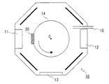
本実施例においてコーティング層の形成は、UBMスパッタ法にて行った。具体的には、以下の通りである。図1は、成膜装置の概略構成を示す模式図である。図1に示す成膜装置10内に複数のアーク蒸発源11、12およびアンバランスドマグネトロンスパッタ蒸発源(以下、UBMスパッタ源と呼ぶ)13を配置し、蒸発源11〜13間の中心点Cを中心としてこれらの蒸発源11〜13間で回転可能な保持具14に基材20である上記切削チップ基材を装着する。
In this example, the coating layer was formed by UBM sputtering. Specifically, it is as follows. FIG. 1 is a schematic diagram showing a schematic configuration of a film forming apparatus. A plurality of
本実施例では、アーク蒸発源11、12に所定の金属原料(例えば、TiAlやSiなど)をセットし、UBMスパッタ源にたとえばSn(錫)をセットした。
In this embodiment, a predetermined metal raw material (for example, TiAl or Si) is set in the
そして、成膜装置10内を真空度1×10⁻³Pa以下に真空引きした後、基材20を500℃まで加熱して1時間保持する。その後、ガス導入口15よりArガスを導入して成膜装置10内を3Paに保った状態で基材20に−1000Vの電圧をかけて、Arガス中でグロー放電を発生させ、Arイオンにより基材20表面をクリーニングする。次に、基材20に所定のバイアス電圧をかけた後、アーク蒸発源11、12を真空アーク放電させて、ガス導入口15よりN2(窒素ガス)、またはN2およびCH4(メタンガス)を成膜装置10内に導入して内層を形成する。次に、ガス導入口15よりAr(アルゴンガス)およびO2(酸素ガス)を成膜装置10内に導入してUBMスパッタ源13を放電させて外層(SnO2層)を形成する。
And after vacuum-evacuating the inside of the film-forming
コーティング層を構成する各層は、放電時間、バイアス電圧、成膜温度、炉内圧力などを調整することで、膜厚、圧縮応力を異ならせた。実施例1〜6では、内層中の圧縮応力が1〜7GPaとなるようにバイアス電圧を−50〜−500V、成膜温度を200〜700℃、炉内圧力1〜5Paにして内層を形成した。各層の圧縮応力は、Cu−Kα線を用いてsin2φ法により測定した。外層の代表的な成膜条件として、実施例1の成膜条件を表2に示す。基本的には外層はUBMスパッタ源により成膜した。 Each layer constituting the coating layer was made different in film thickness and compressive stress by adjusting discharge time, bias voltage, film formation temperature, furnace pressure, and the like. In Examples 1 to 6, the inner layer was formed with a bias voltage of −50 to −500 V, a deposition temperature of 200 to 700 ° C., and a furnace pressure of 1 to 5 Pa so that the compressive stress in the inner layer was 1 to 7 GPa. . The compressive stress of each layer was measured by the sin 2φ method using Cu—Kα rays. Table 2 shows the film formation conditions of Example 1 as typical film formation conditions for the outer layer. Basically, the outer layer was formed by a UBM sputtering source.
上記のように基材上にコーティング層を形成した刃先交換チップを一般的に用いられるホルダに取り付け、これら工具の切削評価を行った。評価は、SCM435からなるブロック状鋼材の上面(300mm×100mm)を切削速度400m/min、切込み量2mm、送り速度0.2mm/刃、乾式で一枚刃のフライス切削加工をセンターカットで行い、逃げ面摩耗幅0.2mmまで切削可能な時間を測定することで行った。測定結果を表3に示す。 The cutting edge replacement chip having the coating layer formed on the substrate as described above was attached to a commonly used holder, and cutting evaluation of these tools was performed. Evaluation is performed on the upper surface (300 mm × 100 mm) of a block-shaped steel material made of SCM435 with a cutting speed of 400 m / min, a cutting depth of 2 mm, a feed rate of 0.2 mm / blade, and a dry single-blade milling with a center cut It was performed by measuring the time during which the flank wear width could be cut to 0.2 mm. Table 3 shows the measurement results.
表1に示す、実施例1〜6,比較例1〜6のコーティング層において、被覆を実施している間、コーティング治具の付着物除去は特に実施しなかったが、異常放電は発生せず、トラブルなくコーティングを完了できた。これは、実施例1〜6の膜の外層は導電性の酸化物膜である効果が現れたものと考えられる。 In the coating layers of Examples 1 to 6 and Comparative Examples 1 to 6 shown in Table 1, during the coating, the deposits on the coating jig were not removed, but no abnormal discharge occurred. The coating was completed without any trouble. This is considered that the effect that the outer layer of the film | membrane of Examples 1-6 is a conductive oxide film appeared.
また、表3から、特定組成の内層、およびZn、In、Sn、Ti、FeまたはVのうちの少なくとも一つの元素の酸化物を30体積%以上含有する導電性酸化物膜からなる外層とを備え、かつ内層中および外層中に圧縮応力を備える実施例1〜6の試料は、合金鋼の高速フライス加工において、優れた耐摩耗性および耐欠損性を発揮することが確認された。 Further, from Table 3, an inner layer having a specific composition and an outer layer made of a conductive oxide film containing at least 30% by volume of an oxide of at least one element of Zn, In, Sn, Ti, Fe, or V It was confirmed that the samples of Examples 1 to 6 provided with compressive stress in the inner layer and the outer layer exhibited excellent wear resistance and fracture resistance in high-speed milling of alloy steel.
(実施例7)
上記実施例4の被覆膜の外層に0.5μmのTiSiCN膜(SUJ2に対する摩擦係数が0.2で赤紫色)を被覆した以外は、実施例4と同一の試料を実施例7として作製した。なお、実施例7において、実施例4のコーティングを行った直後にコーティング治具の付着物除去を実施せずにアーク蒸発源を用いてTiSiCNのコーティングを行ったが、異常な放電現象もなく正常にコーティングを行うことができた。
(Example 7)
A sample identical to Example 4 was prepared as Example 7 except that the outer layer of the coating film of Example 4 was coated with a 0.5 μm TiSiCN film (friction coefficient with respect to SUJ2 of 0.2 and reddish purple). . In Example 7, the coating of TiSiCN was performed using an arc evaporation source without performing the removal of deposits on the coating jig immediately after the coating of Example 4, but it was normal without an abnormal discharge phenomenon. Could be coated.
また、上述と同様の切削条件で切削評価を行ったところ、TiSiCN膜を被覆した実施例7の試料は23パスまで切削可能となり、実施例4の試料の18パスに対して約30%寿命延長できた。このことより、潤滑性を有する(摩擦係数が低い)膜を最外層として被覆した実施例7の試料は優れた切削性能を示し、導電性を有する酸化物膜を外層として被覆するとその直後のコーティングも、異常放電なく安定して成膜できることがわかる。 When the cutting evaluation was performed under the same cutting conditions as described above, the sample of Example 7 coated with the TiSiCN film was able to cut up to 23 passes, and the life was extended by about 30% compared to 18 passes of the sample of Example 4. did it. Thus, the sample of Example 7 in which a film having lubricity (low coefficient of friction) was coated as the outermost layer showed excellent cutting performance, and the coating immediately after the conductive oxide film was coated as the outer layer. It can also be seen that the film can be formed stably without abnormal discharge.
(比較例7)
上記実施例6の外層膜ZnO−50vol%SnO2の代わりにAl2O3を被覆した以外は実施例6と同様に切削工具を作製し、比較例7の切削工具とした。次いで、上述と同様に、比較例7の工具の切削試験を行ったところ、切削性能は16パス切削可能と優れたものであったが、比較例7の膜を被覆した直後、コーティング治具の付着物除去を行わずに実施例1の工具の被覆を再度行ったところ、最内層被覆時に異常放電が発生し、成膜を正常に実施することができなかった。これは、Al2O3の比抵抗が1010Ω・cmより大きく、外層膜が導電性を有さないためであると考えられる。
(Comparative Example 7)
A cutting tool was produced in the same manner as in Example 6 except that Al 2 O 3 was coated instead of the outer layer film ZnO-50 vol% SnO 2 in Example 6 described above, and the cutting tool of Comparative Example 7 was obtained. Subsequently, when the cutting test of the tool of Comparative Example 7 was performed in the same manner as described above, the cutting performance was excellent as 16-pass cutting was possible, but immediately after coating the film of Comparative Example 7, the coating jig When the coating of the tool of Example 1 was performed again without removing the deposits, abnormal discharge occurred when the innermost layer was coated, and the film formation could not be performed normally. This is presumably because the specific resistance of Al 2 O 3 is larger than 10 10 Ω · cm and the outer layer film does not have conductivity.
今回開示された実施の形態および実施例はすべての点で例示であって制限的なものではないと考えられるべきである。本発明の範囲は上記した説明ではなくて特許請求の範囲によって示され、特許請求の範囲と均等の意味および範囲内でのすべての変更が含まれることが意図される。 It should be understood that the embodiments and examples disclosed herein are illustrative and non-restrictive in every respect. The scope of the present invention is defined by the terms of the claims, rather than the description above, and is intended to include any modifications within the scope and meaning equivalent to the terms of the claims.
10 成膜装置、11,12 アーク蒸発源、13 スパッタ源、14 保持具、15 ガス導入口、20 基材。
DESCRIPTION OF
Claims (9)
前記コーティング層は、前記基材側から内層および外層をこの順で備え、
前記内層は、周期律表4a族に属する金属、5a族に属する金属、6a族に属する金属、AlおよびSiからなる群より選択される1種以上の元素と、炭素、窒素および酸素からなる群より選択される1種以上の元素との化合物から構成され、
前記外層は、導電性を有する酸化物膜から構成される、表面被覆切削工具。 A surface-coated cutting tool comprising a coating layer on a substrate,
The coating layer comprises an inner layer and an outer layer in this order from the substrate side,
The inner layer includes a group consisting of a metal belonging to group 4a of the periodic table, a metal belonging to group 5a, a metal belonging to group 6a, one or more elements selected from the group consisting of Al and Si, and carbon, nitrogen and oxygen. Composed of a compound with one or more elements selected from
The outer layer is a surface-coated cutting tool composed of an oxide film having conductivity.
Priority Applications (1)
| Application Number | Priority Date | Filing Date | Title |
|---|---|---|---|
| JP2004270467A JP4812274B2 (en) | 2004-09-16 | 2004-09-16 | Surface coated cutting tool |
Applications Claiming Priority (1)
| Application Number | Priority Date | Filing Date | Title |
|---|---|---|---|
| JP2004270467A JP4812274B2 (en) | 2004-09-16 | 2004-09-16 | Surface coated cutting tool |
Related Child Applications (1)
| Application Number | Title | Priority Date | Filing Date |
|---|---|---|---|
| JP2010257964A Division JP5226060B2 (en) | 2010-11-18 | 2010-11-18 | Method for manufacturing surface-coated cutting tool |
Publications (2)
| Publication Number | Publication Date |
|---|---|
| JP2006082191A true JP2006082191A (en) | 2006-03-30 |
| JP4812274B2 JP4812274B2 (en) | 2011-11-09 |
Family
ID=36161104
Family Applications (1)
| Application Number | Title | Priority Date | Filing Date |
|---|---|---|---|
| JP2004270467A Active JP4812274B2 (en) | 2004-09-16 | 2004-09-16 | Surface coated cutting tool |
Country Status (1)
| Country | Link |
|---|---|
| JP (1) | JP4812274B2 (en) |
Cited By (6)
| Publication number | Priority date | Publication date | Assignee | Title |
|---|---|---|---|---|
| JP2008168421A (en) * | 2006-12-15 | 2008-07-24 | Sandvik Intellectual Property Ab | Coated cemented carbide end mill |
| JP2008183671A (en) * | 2007-01-30 | 2008-08-14 | Sumitomo Electric Hardmetal Corp | Surface-coated cutting tool |
| WO2011089858A1 (en) * | 2010-01-25 | 2011-07-28 | 株式会社神戸製鋼所 | Method for producing tungsten-containing diamond-like carbon film on base of contact probe pin for semiconductor inspection device |
| WO2012008128A1 (en) * | 2010-07-15 | 2012-01-19 | 株式会社神戸製鋼所 | Probe pin for semiconductor inspection devices, method for producing same, and semiconductor inspection method |
| JP2012247287A (en) * | 2011-05-27 | 2012-12-13 | Kobe Steel Ltd | Probe pin for semiconductor inspection device, and manufacturing method thereof |
| JP2014181388A (en) * | 2013-03-19 | 2014-09-29 | Nippon Coating Center Kk | Metal product |
Families Citing this family (1)
| Publication number | Priority date | Publication date | Assignee | Title |
|---|---|---|---|---|
| JP5226060B2 (en) * | 2010-11-18 | 2013-07-03 | 住友電工ハードメタル株式会社 | Method for manufacturing surface-coated cutting tool |
Citations (2)
| Publication number | Priority date | Publication date | Assignee | Title |
|---|---|---|---|---|
| JPS60238481A (en) * | 1984-05-14 | 1985-11-27 | Sumitomo Electric Ind Ltd | Multilayered coated hard metal |
| JPH05177413A (en) * | 1991-12-26 | 1993-07-20 | Sumitomo Electric Ind Ltd | Covered cermet cutting tool and its manufacture |
-
2004
- 2004-09-16 JP JP2004270467A patent/JP4812274B2/en active Active
Patent Citations (2)
| Publication number | Priority date | Publication date | Assignee | Title |
|---|---|---|---|---|
| JPS60238481A (en) * | 1984-05-14 | 1985-11-27 | Sumitomo Electric Ind Ltd | Multilayered coated hard metal |
| JPH05177413A (en) * | 1991-12-26 | 1993-07-20 | Sumitomo Electric Ind Ltd | Covered cermet cutting tool and its manufacture |
Cited By (8)
| Publication number | Priority date | Publication date | Assignee | Title |
|---|---|---|---|---|
| JP2008168421A (en) * | 2006-12-15 | 2008-07-24 | Sandvik Intellectual Property Ab | Coated cemented carbide end mill |
| JP2008183671A (en) * | 2007-01-30 | 2008-08-14 | Sumitomo Electric Hardmetal Corp | Surface-coated cutting tool |
| WO2011089858A1 (en) * | 2010-01-25 | 2011-07-28 | 株式会社神戸製鋼所 | Method for producing tungsten-containing diamond-like carbon film on base of contact probe pin for semiconductor inspection device |
| JP2011149897A (en) * | 2010-01-25 | 2011-08-04 | Kobe Steel Ltd | Method for manufacture tungsten-containing diamond-like carbon coating on base material of contact probe pin for semiconductor inspection device |
| WO2012008128A1 (en) * | 2010-07-15 | 2012-01-19 | 株式会社神戸製鋼所 | Probe pin for semiconductor inspection devices, method for producing same, and semiconductor inspection method |
| JP2012037506A (en) * | 2010-07-15 | 2012-02-23 | Kobe Steel Ltd | Probe pin for semiconductor inspection apparatus, manufacturing method thereof and semiconductor inspection method |
| JP2012247287A (en) * | 2011-05-27 | 2012-12-13 | Kobe Steel Ltd | Probe pin for semiconductor inspection device, and manufacturing method thereof |
| JP2014181388A (en) * | 2013-03-19 | 2014-09-29 | Nippon Coating Center Kk | Metal product |
Also Published As
| Publication number | Publication date |
|---|---|
| JP4812274B2 (en) | 2011-11-09 |
Similar Documents
| Publication | Publication Date | Title |
|---|---|---|
| JP6222675B2 (en) | Surface-coated cutting tool and method for manufacturing the same | |
| US6962751B2 (en) | Amorphous carbon coated tools and method of producing the same | |
| US8075744B1 (en) | Layered coated cutting tool | |
| US8709583B2 (en) | PVD coated tool | |
| EP2276874B1 (en) | A coated cutting tool and a method of making thereof | |
| JP5190971B2 (en) | Coating, cutting tool, and manufacturing method of coating | |
| IL178030A (en) | Surface-coated cutting tool | |
| JP4072155B2 (en) | Surface-coated cutting tool and manufacturing method thereof | |
| JP2005344148A (en) | Wear-resistant film, and surface-coated cutting tool using the same | |
| EP2959994A1 (en) | Surface-coated cutting tool and process for producing same | |
| JP4398224B2 (en) | Wear resistant parts | |
| CN112368094B (en) | Surface-coated cutting tool and method for manufacturing same | |
| JP4812274B2 (en) | Surface coated cutting tool | |
| JP5416429B2 (en) | Surface coated cutting tool | |
| JP5226060B2 (en) | Method for manufacturing surface-coated cutting tool | |
| JP3719709B2 (en) | Amorphous carbon coated tool and method for manufacturing the same | |
| JP3962300B2 (en) | Aluminum oxide coated tool | |
| JP3718664B2 (en) | Amorphous carbon coated tool and method for manufacturing the same | |
| JP3719708B2 (en) | Amorphous carbon coated tool and method for manufacturing the same | |
| CN114761606B (en) | Cutting tool with hard coating film formed thereon | |
| JP6583763B1 (en) | Surface-coated cutting tool and manufacturing method thereof | |
| JP4080481B2 (en) | Surface-coated cutting tool and manufacturing method thereof | |
| JP2005138210A (en) | Surface coated cutting tool | |
| CN116438325A (en) | Hard coating film for cutting tool | |
| JP2006334720A (en) | Coated tool member |
Legal Events
| Date | Code | Title | Description |
|---|---|---|---|
| A625 | Written request for application examination (by other person) |
Free format text: JAPANESE INTERMEDIATE CODE: A625 Effective date: 20070420 |
|
| A977 | Report on retrieval |
Free format text: JAPANESE INTERMEDIATE CODE: A971007 Effective date: 20100218 |
|
| A131 | Notification of reasons for refusal |
Free format text: JAPANESE INTERMEDIATE CODE: A131 Effective date: 20100525 |
|
| A521 | Request for written amendment filed |
Free format text: JAPANESE INTERMEDIATE CODE: A523 Effective date: 20100709 |
|
| A02 | Decision of refusal |
Free format text: JAPANESE INTERMEDIATE CODE: A02 Effective date: 20100824 |
|
| A521 | Request for written amendment filed |
Free format text: JAPANESE INTERMEDIATE CODE: A523 Effective date: 20101118 |
|
| A911 | Transfer to examiner for re-examination before appeal (zenchi) |
Free format text: JAPANESE INTERMEDIATE CODE: A911 Effective date: 20101130 |
|
| A912 | Re-examination (zenchi) completed and case transferred to appeal board |
Free format text: JAPANESE INTERMEDIATE CODE: A912 Effective date: 20101228 |
|
| A521 | Request for written amendment filed |
Free format text: JAPANESE INTERMEDIATE CODE: A523 Effective date: 20110712 |
|
| A01 | Written decision to grant a patent or to grant a registration (utility model) |
Free format text: JAPANESE INTERMEDIATE CODE: A01 |
|
| A61 | First payment of annual fees (during grant procedure) |
Free format text: JAPANESE INTERMEDIATE CODE: A61 Effective date: 20110823 |
|
| R150 | Certificate of patent or registration of utility model |
Ref document number: 4812274 Country of ref document: JP Free format text: JAPANESE INTERMEDIATE CODE: R150 Free format text: JAPANESE INTERMEDIATE CODE: R150 |
|
| FPAY | Renewal fee payment (event date is renewal date of database) |
Free format text: PAYMENT UNTIL: 20140902 Year of fee payment: 3 |
|
| R250 | Receipt of annual fees |
Free format text: JAPANESE INTERMEDIATE CODE: R250 |
|
| R250 | Receipt of annual fees |
Free format text: JAPANESE INTERMEDIATE CODE: R250 |
|
| R250 | Receipt of annual fees |
Free format text: JAPANESE INTERMEDIATE CODE: R250 |
|
| R250 | Receipt of annual fees |
Free format text: JAPANESE INTERMEDIATE CODE: R250 |
|
| R250 | Receipt of annual fees |
Free format text: JAPANESE INTERMEDIATE CODE: R250 |
|
| R250 | Receipt of annual fees |
Free format text: JAPANESE INTERMEDIATE CODE: R250 |
|
| R250 | Receipt of annual fees |
Free format text: JAPANESE INTERMEDIATE CODE: R250 |
|
| R250 | Receipt of annual fees |
Free format text: JAPANESE INTERMEDIATE CODE: R250 |