JP2006066274A - WIRE PRECURSOR OF Nb-Sn COMPOUND SUPERCONDUCTIVE WIRE - Google Patents
WIRE PRECURSOR OF Nb-Sn COMPOUND SUPERCONDUCTIVE WIRE Download PDFInfo
- Publication number
- JP2006066274A JP2006066274A JP2004248614A JP2004248614A JP2006066274A JP 2006066274 A JP2006066274 A JP 2006066274A JP 2004248614 A JP2004248614 A JP 2004248614A JP 2004248614 A JP2004248614 A JP 2004248614A JP 2006066274 A JP2006066274 A JP 2006066274A
- Authority
- JP
- Japan
- Prior art keywords
- based metal
- module
- wire
- filament
- filaments
- Prior art date
- Legal status (The legal status is an assumption and is not a legal conclusion. Google has not performed a legal analysis and makes no representation as to the accuracy of the status listed.)
- Pending
Links
Images


Classifications
-
- H—ELECTRICITY
- H10—SEMICONDUCTOR DEVICES; ELECTRIC SOLID-STATE DEVICES NOT OTHERWISE PROVIDED FOR
- H10N—ELECTRIC SOLID-STATE DEVICES NOT OTHERWISE PROVIDED FOR
- H10N60/00—Superconducting devices
- H10N60/01—Manufacture or treatment
- H10N60/0184—Manufacture or treatment of devices comprising intermetallic compounds of type A-15, e.g. Nb3Sn
-
- H—ELECTRICITY
- H01—ELECTRIC ELEMENTS
- H01K—ELECTRIC INCANDESCENT LAMPS
- H01K1/00—Details
- H01K1/02—Incandescent bodies
-
- H—ELECTRICITY
- H01—ELECTRIC ELEMENTS
- H01K—ELECTRIC INCANDESCENT LAMPS
- H01K3/00—Apparatus or processes adapted to the manufacture, installing, removal, or maintenance of incandescent lamps or parts thereof
- H01K3/02—Manufacture of incandescent bodies
Landscapes
- Engineering & Computer Science (AREA)
- Manufacturing & Machinery (AREA)
- Superconductors And Manufacturing Methods Therefor (AREA)
Abstract
Description
この発明は、高い臨界電流密度(Jc)特性を有しながら、ヒステリシス損失(Qh)特性の増大を抑制し、熱処理を施すことによりNb3Sn超電導線材となるNb−Sn化合物系超電導線の前駆線材に関するものである。 The present invention suppresses an increase in hysteresis loss (Q h ) characteristics while having a high critical current density (Jc) characteristic, and an Nb—Sn compound superconducting wire that becomes an Nb 3 Sn superconducting wire by heat treatment. It relates to a precursor wire.
核融合用大型超電導コイルの実現のためには高い臨界電流密度(Jc)特性と低いヒステリシス損失(Qh)特性を有する超電導線材の開発が必要不可欠であり、特にトロイダル磁場用コイルにはNb3Sn系化合物超電導線材が使用される。超電導線材はその安定化のために、Cu等の抵抗率の小さな金属マトリックス中に数10μm以下の直径の超電導フィラメントが多数埋設された構造が必要で、極細多芯線と呼ばれている。Nb3Sn超電導線の前駆線材は、Cu基金属マトリックス中にSn基金属コアとNb基金属フィラメントが多数埋設された構造をしており、伸線加工後、熱処理することによって、線材中のSn基金属コアがCu基金属マトリックス中に拡散し、さらにNb基金属フィラメント中に拡散することで、Nb基金属フィラメントのまわりあるいは全体にNb3Snが生成され、Nb3Sn超電導線となる。 Development of a superconducting wire having a high critical current density (Jc) characteristic and a low hysteresis loss (Q h ) characteristic is indispensable for realizing a large superconducting coil for fusion. In particular, Nb 3 is used for a toroidal magnetic field coil. Sn compound superconducting wire is used. In order to stabilize the superconducting wire, it requires a structure in which a large number of superconducting filaments having a diameter of several tens of μm or less are embedded in a metal matrix having a small resistivity such as Cu, and is called an ultrafine multi-core wire. The precursor wire of the Nb 3 Sn superconducting wire has a structure in which a large number of Sn-based metal cores and Nb-based metal filaments are embedded in a Cu-based metal matrix. When the base metal core diffuses into the Cu base metal matrix and further diffuses into the Nb base metal filament, Nb 3 Sn is generated around or in the whole of the Nb base metal filament to form an Nb 3 Sn superconducting wire.
従来のNb3Sn超電導線の前駆線材では、上記の熱処理工程において、Sn基金属コアが周囲のCu基金属マトリックス中に拡散することでε相ブロンズ層(Cu3Sn)を形成するが、ε相ブロンズ層の境界(外縁)領域においてNb3Snフィラメントが接触し、Qhが増大するという課題があった。
In the conventional Nb 3 Sn superconducting wire precursor wire, in the heat treatment step, the Sn-based metal core diffuses into the surrounding Cu-based metal matrix to form an ε-phase bronze layer (Cu 3 Sn).
この改良として、ε相ブロンズ層の境界領域で、Nb3Snフィラメントの間隔を他の部分のNb3Snフィラメントの間隔よりも大となるように前駆線材におけるNb基金属フィラメントを配置することで、Qhの増大を抑制しているものが開示されている。(例えば、特許文献1参照)。
As this improvement, at the boundary region of the ε-phase bronze layer, by disposing the Nb base metal filaments in the precursor wire such that the larger than the spacing of
超電導線材でのQh特性の増大原因は、熱処理によって発生するNb3Snフィラメント相互の接触であり、Nb3Snフィラメント相互の接触は、前駆線材の中央部に配置されるSn基金属コアとCu基金属マトリックスとが熱処理によって合金化し、ε相ブロンズ層を生成する領域の境界近傍で生じることが分かっている。特許文献1に示された従来のNb3Sn超電導線の前駆線材では、超電導線材とした時にQh特性の増大原因となる熱処理によって生成されるNb3Snフィラメント相互の接触を防ぐため、ε相ブロンズ層を生成する領域の境界近傍のCu基金属マトリックス中に埋設されるNb基金属フィラメントの間隔を広く取らなければならなかった。より具体的には、ε相ブロンズ層の境界は中心から第3層目と第4層目のNb基金属フィラメントの間に形成されるので、第3層〜第5層のNb基金属フィラメントの直径を前記のようにやや細くして伸線加工後のフィラメント間隔をやや広げていた。その結果、Cu基金属マトリックス中に埋設されるNb基金属フィラメントの量は制限され、前駆線材を熱処理した超電導線材のJcは温度4.2K、磁場12Tで800A/mm2程度に留まり、より高いJc特性を有する線材を得ることが不可能であるという問題点があった。
Increasing cause of Q h characteristics of a superconducting wire is a contact of the
この発明は、上記のような問題点を解決するためになされたものであり、熱処理を施すことにより、高いJc特性を有し、且つ、Qh特性の増大が抑制されたNb3Sn超電導線材となるNb−Sn化合物系超電導線の前駆線材を得ることを目的とするものである。 The present invention has been made in order to solve the above-described problems, and has an Nb 3 Sn superconducting wire that has high Jc characteristics and suppresses an increase in Q h characteristics by heat treatment. It aims at obtaining the precursor wire of the Nb-Sn compound system superconducting wire used.
この発明に係るNb−Sn化合物系超電導線の前駆線材においては、Cu基金属マトリックス中にNb基金属フィラメントとSn基金属コアを埋設したモジュールを複数個備え、上記モジュールの中心部に上記Sn基金属コアを配置し、その周囲に同心状に上記Nb基金属フィラメントを等間隔に分離して配置し、さらにその周囲に上記Nb基金属フィラメントを同心状に順次外周に向かって配置した構造をとり、上記熱処理によって上記Sn基金属コアと上記Cu基金属マトリックスとが反応することにより上記モジュール中に生成するε相ブロンズ層の境界が、上記Nb基金属フィラメントをすべて含むような範囲になるようにSn基金属コアの量が調整されたことを特徴とするものである。 The Nb—Sn compound-based superconducting wire precursor wire according to the present invention includes a plurality of modules in which Nb-based metal filaments and Sn-based metal cores are embedded in a Cu-based metal matrix, and the Sn group is formed at the center of the module. A metal core is arranged, the Nb-based metal filaments are arranged concentrically around the metal core, and the Nb-based metal filaments are arranged concentrically and sequentially toward the outer periphery. The boundary of the ε-phase bronze layer generated in the module by the reaction between the Sn-based metal core and the Cu-based metal matrix by the heat treatment is in a range that includes all the Nb-based metal filaments. The amount of the Sn-based metal core is adjusted.
さらに、上記モジュール中の上記Nb基金属フィラメントが占める体積比率が略0.28以上略0.34以下であり、上記モジュール中の上記Cu基金属マトリックスに対する上記ε相ブロンズ層が占める割合が略0.6以上略0.8以下であり、上記Nb基金属フィラメントの直径が略1μm以上略5μm以下であり、上記Nb基金属フィラメント同士の間隔が略0.7μm以上略1.5μm以下であることを特徴とするものである。 Furthermore, the volume ratio occupied by the Nb-based metal filament in the module is approximately 0.28 or more and approximately 0.34 or less, and the ratio of the ε-phase bronze layer to the Cu-based metal matrix in the module is approximately 0. .6 to about 0.8, the diameter of the Nb-based metal filament is about 1 μm to about 5 μm, and the distance between the Nb-based metal filaments is about 0.7 μm to about 1.5 μm. It is characterized by.
また、この発明の別の前駆線材は、上記熱処理によって上記Sn基金属コアと上記Cu基金属マトリックスとが反応することにより上記モジュール中に生成するε相ブロンズ層の境界が、上記Nb基金属フィラメントの存在領域の略0.05以上略0.35以下の割合を含むような範囲になるようにSn基金属コアの量が調整されたことを特徴とするものである。 Another precursor wire of the present invention is that the boundary of the ε-phase bronze layer generated in the module by the reaction between the Sn-based metal core and the Cu-based metal matrix by the heat treatment is the Nb-based metal filament. The amount of the Sn-based metal core is adjusted so as to be in a range including a ratio of approximately 0.05 to approximately 0.35 in the existing region.
さらに、上記モジュール中の上記Nb基金属フィラメントが占める体積比率が略0.23以上略0.27以下であり、上記モジュール中の上記Cu基金属マトリックスに対する上記ε相ブロンズ層が占める割合が略0.4以上略0.55以下であり、上記Nb基金属フィラメントの直径が略1μm以上略5μm以下であり、上記Nb基金属フィラメント同士の間隔が略0.7μm以上略1.5μm以下であることを特徴とするものである。 Furthermore, the volume ratio occupied by the Nb-based metal filament in the module is approximately 0.23 or more and approximately 0.27 or less, and the ratio of the ε-phase bronze layer to the Cu-based metal matrix in the module is approximately 0. 4 to about 0.55, the diameter of the Nb-based metal filament is about 1 μm to about 5 μm, and the distance between the Nb-based metal filaments is about 0.7 μm to about 1.5 μm. It is characterized by.
この発明によれば、Cu基金属マトリックス中にNb基金属フィラメントとSn基金属コアを埋設したモジュールを複数個備え、上記モジュールの中心部に上記Sn基金属コアを配置し、その周囲に同心状に上記Nb基金属フィラメントを等間隔に分離して配置し、さらにその周囲に上記Nb基金属フィラメントを同心状に順次外周に向かって配置した構造をとり、熱処理によって上記Sn基金属コアと上記Cu基金属マトリックスとが反応することにより上記モジュール中に生成するε相ブロンズ層の境界が、上記Nb基金属フィラメントをすべて含むような範囲になるように上記Sn基金属コアの量が調整されたので、上記ε相ブロンズ層領域の境界は上記Nb基金属フィラメントの存在領域の外側となり、Qh特性の増大原因であるNb3Snフィラメント相互の接触を防ぐことができ、Qh特性の増大を抑制したNb−Sn化合物系超電導線の前駆線材を得ることができる。また、この発明によれば、同じ理由から、Qh特性の増大を抑制するために上記Nb基金属フィラメントの間隔を広く取る必要が無くなること、すなわち、上記Nb基金属フィラメントの量は制限されることがなくなり、前駆線材を熱処理した超電導線材においてNb3Snフィラメントの量が確保されることになり、高いJc特性を有するNb−Sn化合物系超電導線の前駆線材を得ることができる。 According to the present invention, a plurality of modules in which a Nb-based metal filament and a Sn-based metal core are embedded in a Cu-based metal matrix are provided, the Sn-based metal core is disposed at the center of the module, and concentrically around the module. The Nb-based metal filaments are arranged at equal intervals, and the Nb-based metal filaments are arranged concentrically and sequentially toward the outer periphery, and the Sn-based metal core and the Cu are formed by heat treatment. Since the amount of the Sn-based metal core is adjusted so that the boundary of the ε-phase bronze layer generated in the module by reacting with the base metal matrix is in a range that includes all the Nb-based metal filaments. , the boundary of the ε-phase bronze layer region is an outer existence region of the Nb-based metal filaments is increased cause of Q h characteristic N 3 Sn filaments mutual contact that can prevent, it is possible to obtain a precursor wire of Nb-Sn phase superconducting wire that suppresses an increase in the Q h properties. Further, according to the present invention, for the same reasons, the Nb-based metal filaments intervals need not be widely taken in order to suppress an increase in the Q h characteristics, i.e., the amount of the Nb-based metal filaments is limited Thus, the amount of Nb 3 Sn filament is secured in the superconducting wire obtained by heat-treating the precursor wire, and a precursor wire of Nb—Sn compound-based superconducting wire having high Jc characteristics can be obtained.
上記の発明においては、上記モジュール中の上記Nb基金属フィラメントが占める体積比率を略0.28以上略0.34以下、上記モジュール中の上記Cu基金属マトリックスに対する上記ε相ブロンズ層が占める割合が略0.6以上0.8以下、上記Nb基金属フィラメントの直径が略1μm以上略5μm以下、上記Nb基金属フィラメント同士の間隔が略0.7μm以上略1.5μm以下とすることにより、上記ε相ブロンズ層の境界が上記Nb基金属フィラメントの存在領域の外側となり、Nb3Snフィラメント同士の結合がなく、Nb3SnフィラメントとなるNbの量が高い割合で確保されるため、高いJc特性と低いQh特性を有するNb−Sn化合物系超電導線の前駆線材を得ることができる。 In the above invention, the volume ratio occupied by the Nb-based metal filament in the module is about 0.28 or more and about 0.34 or less, and the ratio of the ε-phase bronze layer to the Cu-based metal matrix in the module is When the diameter of the Nb-based metal filament is approximately 1 μm to approximately 5 μm and the distance between the Nb-based metal filaments is approximately 0.7 μm to approximately 1.5 μm, Since the boundary of the ε-phase bronze layer is outside the region where the Nb-based metal filament is present, the Nb 3 Sn filaments are not bonded to each other, and the amount of Nb that becomes the Nb 3 Sn filament is secured at a high rate, so that high Jc characteristics it can be obtained Nb-Sn phase superconducting wire precursor wire having a low Q h characteristics when.
また、この発明の別の発明によれば、上記熱処理によって上記Sn基金属コアと上記Cu基金属マトリックスとが反応することにより上記モジュール中に生成する上記ε相ブロンズ層の境界が、上記Nb基金属フィラメントの存在領域の略0.05以上略0.35以下の割合を含むような範囲になるように上記Sn基金属コアの量が調整されたので、前駆線材を熱処理した超電導線材において、Nb3Snフィラメント相互の接触領域を小さく制限することができ、Qh特性の増大を抑制したNb−Sn化合物系超電導線の前駆線材を得ることができる。また同じ理由から、Qh特性の増大を抑制するために上記Nb基金属フィラメントの間隔を広く取る必要が無くなること、すなわち、上記Nb基金属フィラメントの量は制限されることがなくなり、前駆線材を熱処理した超電導線材においてNb3Snフィラメントの量が確保されることになり、高いJc特性を有するNb−Sn化合物系超電導線の前駆線材を得ることができる。 According to another invention of the present invention, the boundary of the ε-phase bronze layer formed in the module by the reaction between the Sn-based metal core and the Cu-based metal matrix by the heat treatment is the Nb group. Since the amount of the Sn-based metal core is adjusted so as to be in a range including a ratio of approximately 0.05 or more and approximately 0.35 or less of the region where the metal filament exists, in the superconducting wire obtained by heat-treating the precursor wire, Nb 3 Sn filaments mutual contact area can be reduced limits, it is possible to obtain a precursor wire of Nb-Sn phase superconducting wire that suppresses an increase in the Q h properties. For the same reason, Q h characteristics increase the Nb-based metal filaments intervals need not be widely taken in order to inhibit, i.e., the amount of the Nb-based metal filaments no longer be limited, a precursor wire The amount of Nb 3 Sn filament is ensured in the heat-treated superconducting wire, and a precursor wire of Nb—Sn compound-based superconducting wire having high Jc characteristics can be obtained.
上記の発明においては、上記モジュール中の上記Nb基金属フィラメントが占める体積比率を略0.23以上略0.27以下、上記モジュール中の上記Cu基金属マトリックスに対する上記ε相ブロンズ層が占める割合が略0.4以上0.55以下、上記Nb基金属フィラメントの直径が略1μm以上略5μm以下、上記Nb基金属フィラメント同士の間隔が略0.7μm以上略1.5μm以下とすることにより、上記ε相ブロンズ層の境界が上記Nb基金属フィラメントのうち0.05から0.35の割合を含むことになり、Nb3Snフィラメント同士の結合が最小限に抑えられ、かつNb3SnフィラメントとなるNbの量が高い割合で確保されるため、高いJc特性と低いQh特性を有するNb−Sn化合物系超電導線の前駆線材を得ることができる。 In the above invention, the volume ratio occupied by the Nb-based metal filament in the module is about 0.23 or more and about 0.27 or less, and the ratio of the ε-phase bronze layer to the Cu-based metal matrix in the module is When the diameter of the Nb-based metal filament is approximately 1 μm to approximately 5 μm and the distance between the Nb-based metal filaments is approximately 0.7 μm to approximately 1.5 μm, The boundary of the ε-phase bronze layer includes a ratio of 0.05 to 0.35 of the Nb-based metal filament, and the coupling between Nb 3 Sn filaments is minimized and becomes an Nb 3 Sn filament. the amount of Nb is ensured at a high rate, the Nb-Sn phase superconducting wire having a high Jc properties and low Q h characteristics precursor wire Rukoto can.
実施の形態1.
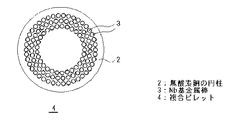
図1は、実施の形態1によるNb−Sn化合物系超電導線の前駆線材の断面図を示しており、図2は実施の形態1による上記前駆線材のモジュール1を製造するための複合ビレットの断面図を示したものである。
FIG. 1 is a cross-sectional view of a precursor wire of an Nb—Sn compound-based superconducting wire according to
実施の形態1の複合ビレット4の製造においては、まず直径140mmの無酸素銅の円柱2に、円柱の中心から半径35mmから51mmにかけて、同心円状に3列の孔を合計106個穿孔する。穿孔した孔には直径6mmのNb基金属棒3を充填し複合ビレット4とした。上記Nb基金属棒は最終的に得られるNb−Sn化合物系超電導線の前駆線材においてNb基金属フィラメント6となる。得られた複合ビレット4を50mmの径に押出し加工し、外周の不要な銅材を切削加工する。さらに中央部の銅の部分に孔を明けて、Sn基金属コア5となるSn基金属棒を挿入する。
In the manufacture of the
Sn基金属棒の直径は最終的に得られる前駆線材を熱処理した際に生成されるε相ブロンズ層の境界位置を決めるものであるが、Cu基金属マトリックス中に生成される上記εブロンズ層領域の体積割合xは、下記の(1)式から求められる。
x=(ε相ブロンズ層領域の体積)÷(Cu基金属マトリックスの体積)
=(Snのモル数)×3÷(Cuのモル数)
=3×(Snの密度)×(モジュール中のSn占有体積比率)÷(Snの原子量)÷
{(Cuの密度)×(モジュール中のCu占有体積比率)÷(Cuの原子量)} (1)
実施の形態1では、Sn基金属棒の直径をそれぞれ、(ア)16.9mm、(イ)19.1mm、(ウ)19.8mm、(エ)20.5mm、(オ)20.9mm、(カ)21.2mm、(キ)21.9mm、(ク)23.4mmとした。これによりε相ブロンズ層のCu基金属マトリックスに対する割合は、それぞれ(ア)0.34、(イ)0.47、(ウ)0.51、(エ)0.58、(オ)0.62、(カ)0.67、(キ)0.71、(ク)0.80となる。
The diameter of the Sn-based metal rod determines the boundary position of the ε-phase bronze layer generated when the finally obtained precursor wire is heat-treated, but the ε-bronze layer region generated in the Cu-based metal matrix Is obtained from the following equation (1).
x = (volume of ε-phase bronze layer region) ÷ (volume of Cu-based metal matrix)
= (Mole number of Sn) × 3 ÷ (Mole number of Cu)
= 3 x (Sn density) x (Sn occupied volume ratio in module) ÷ (Sn atomic weight) ÷
{(Cu density) × (Cu occupied volume ratio in module) ÷ (Cu atomic weight)} (1)
In
Sn基金属棒が挿入された押出し加工後の複合ビレット4は、引抜き加工により縮径加工し、さらに対辺4mmの六角棒に加工することで、モジュール用Cu/Nb/Sn複合棒とした。このCu/Nb/Sn複合棒を切断して37本に束ね、束ねた複合棒はSn拡散バリヤ7となるTaチューブで囲い、上記Taチューブ7の外側を超電導電流の安定化のための安定化銅8となる厚さ7.5mmの無酸素銅チューブで囲う。組み合わされたTaチューブと無酸素銅チューブおよびCu/Nb/Sn複合棒は、0.5mmの径まで引抜き加工を行ってNb−Sn化合物系超電導線の前駆線材9とした。
The
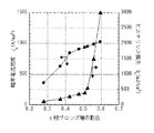
得られた前駆線材から測定用サンプルを切り出し、不活性ガス雰囲気中、650℃で10日間の熱処理を行うことでNb3Sn超電導線材とした。得られた超電導線材の臨界電流密度を液体ヘリウム中、12Tの磁場中で、またヒステリシス損失を液体ヘリウム中、±3Tの変動磁場中で測定すると、上記Sn基金属棒のサイズに依存して、図3に示すような値となった。ここで、ε相ブロンズ層領域の割合xが0.6以上においては、ε相ブロンズ層の境界領域がNb基金属フィラメント6の存在する領域よりも外側となる。換言すれば、Cu基金属マトリックス中にNb基金属フィラメント6とSn基金属コア5が埋設されたモジュール1において、Nb基金属フィラメント6がε相ブロンズ層領域内のみに存在することとなる。図3から明らかなとおり、ε相ブロンズ層領域の割合xが略0.6以上略0.8以下、好ましくは、略0.62以上略0.78以下とすれば、高いJc特性と低いQh特性を有するNb−Sn化合物系超電導線の前駆線材を得ることができる。
A sample for measurement was cut out from the obtained precursor wire and heat treated at 650 ° C. for 10 days in an inert gas atmosphere to obtain an Nb 3 Sn superconducting wire. When the critical current density of the obtained superconducting wire is measured in a magnetic field of 12 T in liquid helium and the hysteresis loss is measured in a magnetic field of ± 3 T in liquid helium, depending on the size of the Sn-based metal rod, The values were as shown in FIG. Here, when the ratio x of the ε-phase bronze layer region is 0.6 or more, the boundary region of the ε-phase bronze layer is outside the region where the Nb-based metal filament 6 exists. In other words, in the
一方、ε相ブロンズ層領域の割合xが0.6より小さい場合、すなわち、前駆線材を300〜600℃で熱処理している際にCu基金属マトリックス中に生成されるε相ブロンズ層の境界領域がNb基金属フィラメント6が存在する領域内に入ってしまう場合は、Qhの増大原因であるNb3Snフィラメント相互の接触が生じ、上記実施の形態1のようにQh特性の増大を抑制することはできない。また、ε相ブロンズ層領域の割合xが0.3程度、すなわち、ε相ブロンズ層の境界領域がNb基金属フィラメント6が存在する領域より内側になると、Qh特性は減少してくるが、Sn基金属コア5の占める体積比率が低くなりすぎて最終的に熱処理によって生成されるNb3Sn量が減るため高Jc特性は得られない。逆に、ε相ブロンズ層領域の割合xが0.8より大きい場合は複合ビレット4におけるSn基金属棒のサイズがNb基金属フィラメント6が存在する領域に重なるため前駆線材は成り立たない。
On the other hand, when the ratio x of the ε-phase bronze layer region is smaller than 0.6, that is, the boundary region of the ε-phase bronze layer generated in the Cu-based metal matrix when the precursor wire is heat-treated at 300 to 600 ° C. If there accidentally get into the area where there are Nb-based metal filaments 6, caused the
実施の形態1における複合ビレット4のNb基金属棒3の直径を6mm、孔の数を106個としたが、最終的な前駆線材でのNb基金属フィラメント6の直径は3μm、Nb基金属フィラメント6同士の間隔は0.9μm、モジュール1内のNb基金属フィラメント6の占める体積比率は0.32となる。上記Nb基金属棒3のサイズや本数については、要求されるJc特性やQh特性によってその設計の範囲内で変更することが可能であるが、本発明における核融合用大型超電導コイルに要求される高Jc/低Qh特性の超電導線材では、モジュール1内のNb基金属フィラメント6の占める体積比率が略0.28以上略0.34以下、好ましくは、略0.30以上略0.33以下であり、Nb基金属フィラメント6の直径が略1μm以上略5μm以下、好ましくは、略2.0μm以上略3.5μm以下であり、Nb基金属フィラメント6同士の間隔が略0.7μm以上略1.5μm以下、好ましくは、略0.8μm以上略1.2μm以下であることが望ましい。
Although the diameter of the Nb-based
モジュール1内のNb基金属フィラメント6の占める体積率が0.28より少ない場合は、最終的に熱処理によってNb基金属フィラメント6とSn基金属コア5が反応することで生成されるNb3Sn量が減り、高Jc特性が得られないばかりでなく、前駆線材を300〜600℃で熱処理している際にマトリックスに生成されるε相ブロンズ層の境界領域がNb基金属フィラメント6が存在する領域内に入ってしまい、Qhの増大原因であるNb3Snフィラメント相互の接触が生じ、上記実施の形態1のようにQh特性の増大を抑制することはできない。逆に、モジュール1内のNb基金属フィラメント6の占める体積率が0.34より多い場合は、Nb基金属フィラメント6同士の間隔を十分確保することができなくなるため、Qhの増大原因であるNb3Snフィラメント相互の接触が生じ、上記実施の形態1のようにQh特性の増大を抑制することはできない。
When the volume ratio occupied by the Nb-based metal filament 6 in the
また、モジュール1内のNb基金属フィラメント6の直径が1μmより細い場合は、フィラメントの一部に断線を生じる可能性が高くなり、上記実施の形態1のような高Jc特性は得られない。逆に、モジュール1内のNb基金属フィラメント6の直径が5μmより太い場合は、最終的に熱処理によってフィラメント全体が反応することができず生成されるNb3Sn量が減り、上記実施の形態1のような高Jc特性は得られない。
Further, when the diameter of the Nb-based metal filament 6 in the
また、モジュール1内のNb基金属フィラメント6同士の間隔が0.7μmより狭い場合は、Qhの増大原因であるNb3Snフィラメント相互の接触が生じ、Qh特性の増大を抑制することはできない。逆に、Nb基金属フィラメント6同士の間隔が1.5μmより広い場合は、Nb基金属フィラメント6の量が減り、最終的に熱処理によって生成されるNb3Sn量が減り、高Jc特性は得られない。
Further, when the distance between the Nb-based metal filaments 6 each other in the
実施の形態1では、Snの拡散バリヤ材としてTaチューブを用いたが、バリヤ材として例えばTa板を管状に加工したものでも実施の形態1と同様の効果を実現することができる。また、Snの拡散バリヤ材の材質としてTaを用いたが、Nb基金属等、Snの拡散を防ぐ効果のある金属であれば、実施の形態1と同様の効果を実現することができる。 In the first embodiment, a Ta tube is used as the Sn diffusion barrier material. However, the same effect as that of the first embodiment can be realized even when the Ta plate is processed into a tubular shape, for example. Further, although Ta is used as the material of the Sn diffusion barrier material, the same effect as in the first embodiment can be realized as long as it is a metal having an effect of preventing Sn diffusion, such as an Nb-based metal.
実施の形態2.
図4は実施の形態2による前駆線材のモジュール1を製造するための複合ビレット4の断面図を示したものである。図4において、図2と同一の符号を付したものは、同一またはこれに相当するものである。
FIG. 4 shows a cross-sectional view of a
実施の形態2の複合ビレット4の製造においては、まず直径140mmの無酸素銅の円柱2に、円柱の中心から半径37mmから52mmにかけて、同心円状に4列の孔を合計224個穿孔する。穿孔した孔に直径3.7mmのNb基金属棒3を充填し複合ビレット4とした。得られた複合ビレット4を実施の形態1と同様に50mmの径に押出し加工し、外周の不要な銅材を切削加工する。さらに中央部の銅の部分に、孔を明けて、Sn基金属コア5となるSn基金属棒を挿入する。
In the manufacture of the
Sn基金属棒の直径は最終的に得られる前駆線材を熱処理した際に生成されるε相ブロンズ層の境界位置を決めるものであるが、Cu基金属マトリックス中に生成される上記εブロンズ層領域の体積割合xは実施の形態1と同様に決められる。実施の形態2では、Sn基金属棒の直径をそれぞれ、(ア)16.4mm、(イ)18.4mm、(ウ)19.4mm、(エ)20.0mm、(オ)20.5mm、(カ)21.2mm、(キ)21.9mm、(ク)22.6mmとした。これによりε相ブロンズ層のCu基金属マトリックスに対する割合は、それぞれ(ア)0.28、(イ)0.37、(ウ)0.42、(エ)0.47、(オ)0.51、(カ)0.52、(キ)0.56、(ク)0.60となる。
The diameter of the Sn-based metal rod determines the boundary position of the ε-phase bronze layer generated when the finally obtained precursor wire is heat-treated, but the ε-bronze layer region generated in the Cu-based metal matrix Is determined in the same manner as in the first embodiment. In
Sn基金属棒が挿入された押出し加工後の複合ビレット4は、実施の形態1と同様に引抜き加工により縮径加工し、さらに対辺5.4mmの六角棒に加工することで、モジュール用Cu/Nb/Sn複合棒とした。このCu/Nb/Sn複合棒を切断して19本に束ね、束ねた複合棒は実施の形態1と同様にSn拡散バリヤ7となるTaチューブで囲い、上記Taチューブ7の外側を超電導電流の安定化のための安定化銅8となる厚さ7.5mmの無酸素銅チューブで囲う。組み合わされたTaチューブと無酸素銅チューブおよびCu/Nb/Sn複合棒は、0.5mmの径まで引抜き加工を行ってNb−Sn化合物系超電導線の前駆線材9とした。
The
得られた前駆線材から測定用サンプルを切り出し、実施の形態1と同様に不活性ガス雰囲気中、650℃で10日間の熱処理を行うことでNb3Sn超電導線材とした。得られた超電導線材の臨界電流密度を液体ヘリウム中、12Tの磁場中で、またヒステリシス損失を液体ヘリウム中、±3Tの変動磁場中で測定すると、上記Sn基金属棒のサイズに依存して、図5に示すような値となった。ここで、ε相ブロンズ層領域の割合xが0.4の場合、ε相ブロンズ層の境界領域にあるNb基金属フィラメント6の割合が0.08となる。また、ε相ブロンズ層領域の割合xが0.55の場合、ε相ブロンズ層の境界領域内にあるNb基金属フィラメント6の存在割合が0.32となる。図5から明らかなとおり、ε相ブロンズ層領域の割合xが略0.4以上略0.55以下、好ましくは、略0.45以上略0.52以下とすれば、低いQh特性を有し、かつJcの低減が抑えられたNb−Sn化合物系超電導線の前駆線材を得ることができる。 A sample for measurement was cut out from the obtained precursor wire, and a Nb 3 Sn superconducting wire was obtained by performing heat treatment at 650 ° C. for 10 days in an inert gas atmosphere as in the first embodiment. When the critical current density of the obtained superconducting wire is measured in a magnetic field of 12 T in liquid helium and the hysteresis loss is measured in a magnetic field of ± 3 T in liquid helium, depending on the size of the Sn-based metal rod, The values were as shown in FIG. Here, when the ratio x of the ε-phase bronze layer region is 0.4, the ratio of the Nb-based metal filament 6 in the boundary region of the ε-phase bronze layer is 0.08. When the ratio x of the ε phase bronze layer region is 0.55, the existence ratio of the Nb-based metal filament 6 in the boundary region of the ε phase bronze layer is 0.32. As apparent from FIG. 5, the ratio x of the ε-phase bronze layer region is substantially 0.4 to substantially 0.55 or less, preferably, if substantially 0.45 or more substantially 0.52, have a low Q h properties And the precursor wire of the Nb-Sn compound system superconducting wire by which reduction of Jc was suppressed can be obtained.
一方、ε相ブロンズ層領域の割合xが0.4より小さい場合、すなわち、前駆線材を300〜600℃で熱処理している際にCu基金属マトリックス中に生成されるε相ブロンズ層の境界領域が、Nb基金属フィラメント6が存在する領域よりも内側に入ってしまう場合は、Qh特性は小さくなるが、Sn基金属コア5の占める体積比率が低くなりすぎてしまい、熱処理によって生成するNb3Snの量が小さく、高Jc特性は得られない。また、ε相ブロンズ層領域の割合xが0.55より大きい場合は、Qhの増大原因であるNb3Snフィラメント相互の接触が広範囲に生じ、Qh特性の増大を防ぐことはできない。
On the other hand, when the ratio x of the ε phase bronze layer region is smaller than 0.4, that is, the boundary region of the ε phase bronze layer generated in the Cu-based metal matrix when the precursor wire is heat-treated at 300 to 600 ° C. Nb but if from a region where the Nb-based metal filaments 6 are present accidentally get inside, but Q h characteristic becomes small, the volume ratio occupied by the Sn-based metal core 5 becomes too low, produced by heat treatment The amount of 3 Sn is small, and high Jc characteristics cannot be obtained. Also, if a greater proportion x of ε phase bronze layer region is 0.55,
実施の形態2における複合ビレット4のNb基金属棒3の直径を3.7mm、孔の数を224個としたが、最終的な前駆線材でのNb基金属フィラメント6の直径は2.6μm、Nb基金属フィラメント6同士の間隔は0.9μm、モジュール内のNb基金属フィラメント6の占める体積比率は0.25となる。上記Nb基金属棒3のサイズや本数については、要求されるJc特性やQh特性によってその設計の範囲内で変更することが可能であるが、本発明における核融合用大型超電導コイルに要求される高Jc/低Qh特性の超電導線材では、モジュール内のNb基金属フィラメント6の占める体積比率が略0.23以上略0.27以下、好ましくは、略0.24以上略0.26以下であり、Nb基金属フィラメント6の直径が略1μm以上略5μm以下、好ましくは、略2.0μm以上略3.5μm以下であり、Nb基金属フィラメント6同士の間隔が略0.7μm以上略1.5μm以下、好ましくは、略0.8μm以上略1.2μm以下であることが望ましい。
Although the diameter of the Nb-based
モジュール1内のNb基金属フィラメント6の占める体積比率が0.23より少ない場合は、最終的に熱処理によってNb基金属フィラメント6とSn基金属コア5が反応することで生成されるNb3Sn量が減り、高Jc特性が得られない。逆に、モジュール1内のNb基金属フィラメント6の占める体積比率が0.27より多い場合は、熱処理により生成されるε相ブロンズ層の境界領域がNb基金属フィラメント6の存在領域内に入る割合の増大を抑えられず、またNb基金属フィラメント6同士の間隔を十分に確保することができなくなるため、Qhの増大原因であるNb3Snフィラメント相互の接触が生じ、上記実施の形態2のようにQh特性の増大を抑制することはできない。
When the volume ratio occupied by the Nb-based metal filament 6 in the
また、モジュール1内のNb基金属フィラメント6の直径が1μmより細い場合は、フィラメントの一部に断線を生じる可能性が高くなり、上記実施の形態2のような高Jc特性は得られない。逆に、モジュール内のNb基金属フィラメント6の直径が5μmより太い場合は、最終的に熱処理によってフィラメント全体が反応することができず生成されるNb3Sn量が減り、上記実施の形態2のような高Jc特性は得られない。
Further, when the diameter of the Nb-based metal filament 6 in the
また、モジュール1内のNb基金属フィラメント6同士の間隔が0.7μmより狭い場合は、Qhの増大原因であるNb3Snフィラメント相互の接触が生じ、Qh特性の増大を抑制することはできない。逆に、Nb基金属フィラメント6同士の間隔が1.5μmより広い場合は、Nb基金属フィラメント6の量が減り、最終的に熱処理によって生成されるNb3Sn量が減り、高Jc特性は得られない。
Further, when the distance between the Nb-based metal filaments 6 each other in the
実施の形態2では、Snの拡散バリヤ材としてTaチューブを用いたが、バリヤ材として例えばTa板を管状に加工したものでも上記実施の形態2と同様の効果を実現することができる。また、Snの拡散バリヤ材の材質としてTaを用いたが、Nb基金属等、Snの拡散を防ぐ効果のある金属であれば、実施の形態2と同様の効果を実現することができる。 In the second embodiment, a Ta tube is used as the Sn diffusion barrier material. However, the same effect as in the second embodiment can be realized even when the Ta plate is processed into a tubular shape, for example. Further, although Ta is used as the material of the Sn diffusion barrier material, the same effects as those of the second embodiment can be realized as long as the metal has an effect of preventing the diffusion of Sn, such as an Nb-based metal.
なお、本発明において、Cu基金属とは、純Cu、または約2重量%以下のSnを含むCuをいう。 In the present invention, the Cu-based metal refers to pure Cu or Cu containing about 2 wt% or less of Sn.
また、Nb基金属とは、純Nb、または約10重量%以下のTa、約5重量%以下のTiのうち少なくとも何れか一種を含むNbをいう。 The Nb-based metal refers to Nb containing at least one of pure Nb or about 10 wt% or less of Ta or about 5 wt% or less of Ti.
さらにまた、Sn基金属とは、純Sn、または約5重量%以下のTi、約2重量%以下のCu、約2重量%以下のInのうち少なくとも何れか一種を含むSnをいう。 Furthermore, the Sn-based metal refers to Sn containing at least one of pure Sn or about 5 wt% or less of Ti, about 2 wt% or less of Cu, or about 2 wt% or less of In.
1 モジュール、2 無酸素銅の円柱、3 Nb基金属棒、4 複合ビレット、5 Sn基金属コア、6 Nb基金属フィラメント、7 Sn拡散バリヤ、8 安定化銅、9 Nb−Sn化合物系超電導線の前駆線材。 1 module, 2 oxygen-free copper cylinder, 3 Nb-based metal rod, 4 composite billet, 5 Sn-based metal core, 6 Nb-based metal filament, 7 Sn diffusion barrier, 8 stabilized copper, 9 Nb-Sn compound superconducting wire Precursor wire.
Claims (4)
上記モジュールは、その中心部に上記Sn基金属コアを配置し、その周囲に同心状に上記Nb基金属フィラメントを等間隔に分離して配置し、さらにその周囲に上記Nb基金属フィラメントを同心状に順次外周に向かって配置した構造をとり、
上記熱処理によって上記Sn基金属コアと上記Cu基金属マトリックスとが反応することにより上記モジュール中に生成するε相ブロンズ層の境界が、上記Nb基金属フィラメントをすべて含むような範囲になるように、上記Sn基金属コアの量が調整されたことを特徴とするNb−Sn化合物系超電導線の前駆線材。 In the precursor wire of the Nb-Sn compound system superconducting wire, which comprises a plurality of modules in which a Nb-based metal filament and a Sn-based metal core are embedded in a Cu-based metal matrix, and becomes a Nb 3 Sn superconducting wire by heat treatment,
In the module, the Sn-based metal core is arranged at the center, the Nb-based metal filaments are arranged in a concentric manner at equal intervals, and the Nb-based metal filament is concentrically arranged around the core. The structure is arranged sequentially toward the outer periphery,
The boundary of the ε-phase bronze layer generated in the module by the reaction between the Sn-based metal core and the Cu-based metal matrix by the heat treatment is in a range that includes all the Nb-based metal filaments. A precursor wire for a Nb-Sn compound-based superconducting wire, wherein the amount of the Sn-based metal core is adjusted.
上記モジュール中の上記Nb基金属フィラメントが占める体積比率が略0.28以上略0.34以下であり、
上記モジュール中の上記Cu基金属マトリックスに対する上記ε相ブロンズ層が占める割合が略0.6以上略0.8以下であり、
上記Nb基金属フィラメントの直径が略1μm以上略5μm以下であり、
上記Nb基金属フィラメント同士の間隔が略0.7μm以上略1.5μm以下であることを特徴とする、請求項1に記載のNb−Sn化合物系超電導線の前駆線材。 A module in which a Nb-based metal filament and a Sn-based metal core are embedded in a Cu-based metal matrix,
The volume ratio occupied by the Nb-based metal filament in the module is about 0.28 or more and about 0.34 or less,
The ratio of the ε-phase bronze layer to the Cu-based metal matrix in the module is about 0.6 or more and about 0.8 or less,
The diameter of the Nb-based metal filament is about 1 μm to about 5 μm,
2. The precursor wire for an Nb—Sn compound-based superconducting wire according to claim 1, wherein an interval between the Nb-based metal filaments is approximately 0.7 μm or more and approximately 1.5 μm or less.
上記モジュールは、その中心部に上記Sn基金属コアを配置し、その周囲に同心状に上記Nb基金属フィラメントを等間隔に分離して配置し、さらにその周囲に上記Nb基金属フィラメントを同心状に順次外周に向かって配置した構造をとり、
上記熱処理によって上記Sn基金属コアと上記Cu基金属マトリックスとが反応することにより上記モジュール中に生成するε相ブロンズ層の境界が、上記Nb基金属フィラメントの存在領域の略0.08以上略0.32以下の割合を含むような範囲になるように、上記Sn基金属コアの量が調整されたことを特徴とするNb−Sn化合物系超電導線の前駆線材。 In the precursor wire of the Nb-Sn compound system superconducting wire, which comprises a plurality of modules in which a Nb-based metal filament and a Sn-based metal core are embedded in a Cu-based metal matrix, and becomes a Nb 3 Sn superconducting wire by heat treatment,
In the module, the Sn-based metal core is arranged at the center, the Nb-based metal filaments are arranged in a concentric manner at equal intervals, and the Nb-based metal filament is concentrically arranged around the core. The structure is arranged sequentially toward the outer periphery,
The boundary between the ε-phase bronze layers formed in the module due to the reaction between the Sn-based metal core and the Cu-based metal matrix by the heat treatment is approximately 0.08 or more and approximately 0 of the existence region of the Nb-based metal filament. A precursor wire of an Nb—Sn compound-based superconducting wire, wherein the amount of the Sn-based metal core is adjusted so as to be in a range including a ratio of .32 or less.
上記モジュール中の上記Nb基金属フィラメントが占める体積比率が略0.23以上略0.27以下であり、
上記モジュール中の上記Cu基金属マトリックスに対する上記ε相ブロンズ層が占める割合が略0.4以上略0.55以下であり、
上記Nb基金属フィラメントの直径が略1μm以上略5μm以下であり、
上記Nb基金属フィラメント同士の間隔が略0.7μm以上略1.5μm以下であることを特徴とする、請求項3に記載のNb−Sn化合物系超電導線の前駆線材。
A module in which a Nb-based metal filament and a Sn-based metal core are embedded in a Cu-based metal matrix,
The volume ratio occupied by the Nb-based metal filament in the module is about 0.23 or more and about 0.27 or less,
The ratio of the ε-phase bronze layer to the Cu-based metal matrix in the module is about 0.4 or more and about 0.55 or less,
The diameter of the Nb-based metal filament is about 1 μm to about 5 μm,
The Nb-Sn compound-based superconducting wire precursor wire according to claim 3, wherein an interval between the Nb-based metal filaments is approximately 0.7 µm or more and approximately 1.5 µm or less.
Priority Applications (4)
| Application Number | Priority Date | Filing Date | Title |
|---|---|---|---|
| JP2004248614A JP2006066274A (en) | 2004-08-27 | 2004-08-27 | WIRE PRECURSOR OF Nb-Sn COMPOUND SUPERCONDUCTIVE WIRE |
| US11/156,590 US20060289836A1 (en) | 2004-08-27 | 2005-06-21 | Precursor wire of Nb-Sn phase superconducting wire |
| FR0508608A FR2877493A1 (en) | 2004-08-27 | 2005-08-18 | PRECURSOR METAL WIRE OF A Nb-Sn SUPERCONDUCTING METAL WIRE. |
| KR1020050078336A KR100724212B1 (en) | 2004-08-27 | 2005-08-25 | PRECURSOR WIRE OF Nb-Sn PHASE SUPERCONDUCTING WIRE |
Applications Claiming Priority (1)
| Application Number | Priority Date | Filing Date | Title |
|---|---|---|---|
| JP2004248614A JP2006066274A (en) | 2004-08-27 | 2004-08-27 | WIRE PRECURSOR OF Nb-Sn COMPOUND SUPERCONDUCTIVE WIRE |
Publications (2)
| Publication Number | Publication Date |
|---|---|
| JP2006066274A true JP2006066274A (en) | 2006-03-09 |
| JP2006066274A5 JP2006066274A5 (en) | 2006-05-18 |
Family
ID=36112572
Family Applications (1)
| Application Number | Title | Priority Date | Filing Date |
|---|---|---|---|
| JP2004248614A Pending JP2006066274A (en) | 2004-08-27 | 2004-08-27 | WIRE PRECURSOR OF Nb-Sn COMPOUND SUPERCONDUCTIVE WIRE |
Country Status (4)
| Country | Link |
|---|---|
| US (1) | US20060289836A1 (en) |
| JP (1) | JP2006066274A (en) |
| KR (1) | KR100724212B1 (en) |
| FR (1) | FR2877493A1 (en) |
Cited By (1)
| Publication number | Priority date | Publication date | Assignee | Title |
|---|---|---|---|---|
| US7821514B2 (en) | 2006-05-11 | 2010-10-26 | Kabushiki Kaisha Toshiba | Image processing apparatus, image processing method, and image processing program |
Families Citing this family (3)
| Publication number | Priority date | Publication date | Assignee | Title |
|---|---|---|---|---|
| JP2007128686A (en) * | 2005-11-01 | 2007-05-24 | Kobe Steel Ltd | Nb3Sn SUPERCONDUCTING WIRE MATERIAL MANUFACTURED BY INSIDE DIFFUSION METHOD |
| JP5671324B2 (en) * | 2010-12-14 | 2015-02-18 | 株式会社Shカッパープロダクツ | Nb3Sn superconducting wire precursor, method for producing Nb3Sn superconducting wire precursor, Nb3Sn superconducting wire, and superconducting magnet system |
| JP6928595B2 (en) * | 2018-11-09 | 2021-09-01 | 株式会社神戸製鋼所 | Precursors used in the manufacture of superconducting wires, methods for manufacturing precursors, and superconducting wires |
Family Cites Families (5)
| Publication number | Priority date | Publication date | Assignee | Title |
|---|---|---|---|---|
| JP3012436B2 (en) * | 1993-04-02 | 2000-02-21 | 三菱電機株式会社 | Compound based superconducting wire and its manufacturing method |
| JP3510351B2 (en) * | 1994-11-08 | 2004-03-29 | 古河電気工業株式会社 | A3 Method for producing B-type compound superconducting wire |
| JP4013335B2 (en) | 1998-06-09 | 2007-11-28 | 三菱電機株式会社 | Nb3Sn compound superconductor precursor wire and method for manufacturing the same, Nb3Sn compound superconductor conductor manufacturing method, and Nb3Sn compound superconductor coil manufacturing method |
| JP2004342561A (en) | 2003-05-19 | 2004-12-02 | Kobe Steel Ltd | Nb3sn superconductive wire |
| EP1719190B1 (en) * | 2004-02-19 | 2010-05-19 | Oxford Superconducting Technology | Improving critical current density in Nb3Sn superconducting wire |
-
2004
- 2004-08-27 JP JP2004248614A patent/JP2006066274A/en active Pending
-
2005
- 2005-06-21 US US11/156,590 patent/US20060289836A1/en not_active Abandoned
- 2005-08-18 FR FR0508608A patent/FR2877493A1/en active Pending
- 2005-08-25 KR KR1020050078336A patent/KR100724212B1/en not_active IP Right Cessation
Cited By (1)
| Publication number | Priority date | Publication date | Assignee | Title |
|---|---|---|---|---|
| US7821514B2 (en) | 2006-05-11 | 2010-10-26 | Kabushiki Kaisha Toshiba | Image processing apparatus, image processing method, and image processing program |
Also Published As
| Publication number | Publication date |
|---|---|
| KR100724212B1 (en) | 2007-05-31 |
| US20060289836A1 (en) | 2006-12-28 |
| FR2877493A1 (en) | 2006-05-05 |
| KR20060050657A (en) | 2006-05-19 |
Similar Documents
| Publication | Publication Date | Title |
|---|---|---|
| US6981309B2 (en) | Method for producing (Nb, Ti)3Sn wire by use of Ti source rods | |
| JP5588303B2 (en) | Precursor of Nb3Sn superconducting wire and Nb3Sn superconducting wire using the same | |
| JP2007524210A (en) | Improvement of critical density in Nb3Sn superconducting wire | |
| JP6934878B2 (en) | Method for manufacturing multifilament Nb3Sn superconducting wire | |
| US5753862A (en) | Compound superconducting wire and method for manufacturing the same | |
| JP2006004684A (en) | Manufacturing method of superconductive wire rod | |
| KR100724212B1 (en) | PRECURSOR WIRE OF Nb-Sn PHASE SUPERCONDUCTING WIRE | |
| JP2010015821A (en) | Precursor for manufacturing nb3sn superconductive wire rod and method of manufacturing the same, and nb3sn superconductive wire rod | |
| US9037203B2 (en) | Composite barrier-type Nb3AI superconducting multifilament wire material | |
| US20070004597A1 (en) | Nb-Sn phase superconducting wire and precursor wire thereof | |
| US4094059A (en) | Method for producing composite superconductors | |
| JP5805469B2 (en) | Precursor for producing Nb3Sn superconducting wire and Nb3Sn superconducting wire | |
| JPS6137764B2 (en) | ||
| JP4402815B2 (en) | Nb3Al superconducting multi-core wire and manufacturing method thereof | |
| JP2013062039A (en) | PRECURSOR FOR MANUFACTURING Nb3Sn SUPERCONDUCTING WIRE ROD AND Nb3Sn SUPERCONDUCTING WIRE ROD | |
| EP3961658A1 (en) | Blank for producing a long nb3 sn-based superconducting wire | |
| JP3920606B2 (en) | Powder method Nb (3) Method for producing Sn superconducting wire | |
| JP2009004128A (en) | BRONZE-PROCESS Nb3Sn SUPERCONDUCTING WIRE, AND PRECURSOR THEREOF | |
| JP2007027089A (en) | Superconductive element containing copper inclusion, complex material, and manufacturing method of the same | |
| JP2007149494A (en) | METHOD OF MANUFACTURING Nb3Sn SUPERCONDUCTIVE WIRE, AND PRECURSOR THEREFOR | |
| JP4723345B2 (en) | Method for producing Nb3Sn superconducting wire and precursor therefor | |
| JP3127181B2 (en) | Method for manufacturing composite superconducting wire and method for manufacturing composite superconducting coil | |
| KR102396965B1 (en) | Method of manufacturing superconductor | |
| US6810276B1 (en) | Method to reduce magnetization in high current density superconductors formed by reaction of multi-component elements in filamentary composite superconductors | |
| JP2008166173A (en) | Nb3Sn SUPERCONDUCTIVE WIRE, PRECURSOR THEREFOR, AND Nb COMPOUND SINGLE CORE FOR PRECURSOR |
Legal Events
| Date | Code | Title | Description |
|---|---|---|---|
| A521 | Request for written amendment filed |
Free format text: JAPANESE INTERMEDIATE CODE: A523 Effective date: 20051212 |
|
| A621 | Written request for application examination |
Free format text: JAPANESE INTERMEDIATE CODE: A621 Effective date: 20051212 |
|
| A521 | Request for written amendment filed |
Free format text: JAPANESE INTERMEDIATE CODE: A523 Effective date: 20060329 |
|
| A977 | Report on retrieval |
Free format text: JAPANESE INTERMEDIATE CODE: A971007 Effective date: 20080104 |
|
| A131 | Notification of reasons for refusal |
Free format text: JAPANESE INTERMEDIATE CODE: A131 Effective date: 20090224 |
|
| A02 | Decision of refusal |
Free format text: JAPANESE INTERMEDIATE CODE: A02 Effective date: 20090630 |