JP2006058799A - Integrated circuit for driving display device - Google Patents
Integrated circuit for driving display device Download PDFInfo
- Publication number
- JP2006058799A JP2006058799A JP2004243102A JP2004243102A JP2006058799A JP 2006058799 A JP2006058799 A JP 2006058799A JP 2004243102 A JP2004243102 A JP 2004243102A JP 2004243102 A JP2004243102 A JP 2004243102A JP 2006058799 A JP2006058799 A JP 2006058799A
- Authority
- JP
- Japan
- Prior art keywords
- delay time
- signal
- display device
- integrated circuit
- output
- Prior art date
- Legal status (The legal status is an assumption and is not a legal conclusion. Google has not performed a legal analysis and makes no representation as to the accuracy of the status listed.)
- Pending
Links
Images


Abstract
Description
本発明は表示装置駆動用集積回路に関し、特に、例えば、プラズマディスプレイパネルのような、フラットパネルディスプレイを駆動する表示装置駆動用集積回路に関する。 The present invention relates to an integrated circuit for driving a display device, and more particularly to an integrated circuit for driving a display device that drives a flat panel display such as a plasma display panel.
近年、プラズマディスプレイパネル(以下PDPと称する)を用いた大画面、薄型の壁掛けテレビが脚光を浴びている。
図5は、PDPを駆動するためのPDP駆動装置の概略の構成例を示す図である。
In recent years, large-screen, thin wall-mounted televisions using plasma display panels (hereinafter referred to as PDPs) have attracted attention.
FIG. 5 is a diagram illustrating a schematic configuration example of a PDP driving device for driving a PDP.
なお、ここでは簡単のため、2電極のPDPの例を示している。
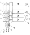
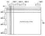
PDP700の駆動装置は複数のスキャンドライバIC(Integrated Circuit)800−1、800−2、800−3、…、800−kと、データ(アドレス)ドライバIC900−1、900−2、900−3、…、900−lなど(ここでk,lは任意の数である)から構成される。
For simplicity, an example of a two-electrode PDP is shown here.
The PDP 700 has a plurality of scan driver ICs (Integrated Circuits) 800-1, 800-2, 800-3,..., 800-k, and data (address) driver ICs 900-1, 900-2, 900-3, ..., 900-l, etc. (where k and l are arbitrary numbers).
スキャンドライバIC800−1〜800−kは、それぞれ複数本の走査・維持電極911を駆動し、データ(アドレス)ドライバIC900−1〜900−lは、それぞれ、R、G、Bの各色に対応する複数本のデータ電極912を駆動する。この走査・維持電極911と、データ電極912とは互いに垂直になるように格子状に配置され、その交点に放電セル(図示せず)が配置される。
Each of the scan driver ICs 800-1 to 800-k drives a plurality of scan / sustain
スキャンドライバIC800−1〜800−kの数は、例えば、それぞれ64本の走査・維持電極911を駆動可能とすると、XGA(eXtended video Graphics Array)の場合、PDP700の画素数は1024×768であるので、k=12個配置されることになる。
For example, if the number of scan driver ICs 800-1 to 800-k can drive 64 scan / sustain
画像の表示の際には、これらのスキャンドライバIC800−1〜800−k、データ(アドレス)ドライバIC900−1〜900−lによって、データ電極912からのデータを、放電セルに走査・維持電極911ごとにスキャンして書き込み(アドレス放電期間)、走査・維持電極911に放電維持パルスを数回出力して放電を維持(放電維持期間)し、画像の表示を行う。
In displaying an image, the scan driver ICs 800-1 to 800-k and the data (address) driver ICs 900-1 to 900-l use the scan driver ICs 9-1 to 900-1 to transfer data from the
図6は、従来の表示装置駆動用集積回路の構成図である。
なお、ここでは、スキャンドライバICの例を示している。
スキャンドライバIC800は、図5で示した走査・維持電極911を制御するシリアル信号を端子DATAより入力し、端子CLKに入力されるクロック信号に同期させてパラレル信号に変換するシフトレジスタ810−1、810−2、810−3、…、810−nと、シフトレジスタ810−1、810−2、810−3、…、810−nからビットごとに転送された信号を、出力段回路830−1、830−2、830−3、…、830−nに送出するデータセレクタ820−1、820−2、820−3、…、820−nを有する。nは任意の数であり、例えば、64ビットのスキャンドライバIC800の場合は、n=64となり、64本の走査・維持電極911を駆動する。
FIG. 6 is a block diagram of a conventional integrated circuit for driving a display device.
Here, an example of a scan driver IC is shown.
The
なお、データセレクタ820−1、820−2、820−3、…、820−nに接続される端子SH及び端子SLには、放電維持期間において、端子SHには、全ての走査・維持電極911を、H(High)レベルにする際の全出力Hレベル固定信号が入力され、端子SLには、全ての走査・維持電極911を、L(Low)レベルにする際の全出力Lレベル固定信号が入力される。
Note that the terminals SH and SL connected to the data selectors 820-1, 820-2, 820-3,..., 820-n are in the discharge sustain period, and all the scan / sustain
また、このほかにも、過熱防止のための温度検出回路を追加集積化したドライバICが、例えば、特許文献1に開示されている。
図7は、従来の表示装置駆動用集積回路の動作を説明するタイミング図である。
In addition, for example,
FIG. 7 is a timing chart for explaining the operation of a conventional display device driving integrated circuit.
この図では、アドレス放電期間において、端子CLKに入力されるクロック信号、出力段回路830−1、830−2、830−3、…、830−nの出力端子Do1〜Donの出力波形(Do1〜Don出力波形)を示している。 In this figure, during the address discharge period, the clock signal input to the terminal CLK, the output waveforms (Do1 to Do1) of the output terminals Do1 to Don of the output stage circuits 830-1, 830-2, 830-3,. Don output waveform).
アドレス放電期間には、端子DATAからの信号が、クロック信号の立ち上がりに同期して、シフトレジスタ810−1、810−2、810−3、…、810−nによりビットごとに取り込まれる。そして、データセレクタ820−1〜820−nを介して順に出力段回路830−1〜830−nに入力される。これにより、出力段回路830−1〜830−nの出力波形は図のように、クロック信号の立ち上がりに同期して順に立ち下がり、次のクロック信号の立ち上がりで再び立ち上がる波形となる。なお、ここでは、図示を省略しているが、実際には、出力段回路830−1〜830−nにおける伝播遅延によって、クロック信号の立ち上がりから、出力信号が出力されるまでには、所定の伝播遅延時間を有する。 In the address discharge period, the signal from the terminal DATA is taken in for each bit by the shift registers 810-1, 810-2, 810-3, ..., 810-n in synchronization with the rising edge of the clock signal. Then, the data are sequentially input to the output stage circuits 830-1 to 830-n via the data selectors 820-1 to 820-n. As a result, the output waveforms of the output stage circuits 830-1 to 830-n become waveforms that sequentially fall in synchronization with the rise of the clock signal and rise again at the rise of the next clock signal, as shown in the figure. Although illustration is omitted here, in practice, a predetermined delay occurs between the rising edge of the clock signal and the output of the output signal due to the propagation delay in the output stage circuits 830-1 to 830-n. Has propagation delay time.
図8は、従来の表示装置駆動用集積回路における出力段回路の回路図である。
出力段回路830は、レベルシフタ回路831と、インバータ832、833と、バッファ回路834と、走査・維持電極911を直接駆動する2つのIGBT(Insulated Gate Bipolar Transistor)835、836を有している。なお、インバータ832、833及びバッファ回路834は適当な遅延時間を有しており、スイッチング時の貫通電流防止を図っている。貫通電流を防止する技術は、更に例えば特許文献2に開示されている。
FIG. 8 is a circuit diagram of an output stage circuit in a conventional display device driving integrated circuit.
The
レベルシフタ回路831は、高耐圧のpチャンネル型MOSFET(Metal Oxide Semiconductor Field Effect Transistor)(以下PMOSと称する)831a、831bと、nチャンネル型MOSFET(以下NMOSと称する)831c、831dから構成される回路である。PMOS831aは、ソース端子を0〜100Vの高電圧を供給する高電圧電源端子VDHに、ドレイン端子をNMOS831cのドレイン端子、PMOS831bのゲート端子及びIGBT836のゲート端子に接続している。PMOS831aのゲート端子は、PMOS831bのドレイン端子及びNMOS831dのドレイン端子と接続されている。また、PMOS831bも同様に、ソース端子を高電圧電源端子VDHに接続しており、ドレイン端子はNMOS831dのドレイン端子及びPMOS831aのゲート端子に接続している。PMOS831bのゲート端子は、PMOS831aのドレイン端子と接続されている。また、NMOS831c、831dのソース端子はともに接地される。また、NMOS831cのゲート端子にはインバータ832を介して、NMOS831dのゲート端子にはインバータ832、833を介して、入力端子INからの信号(前述のデータセレクタ820−1〜820−nからの送出された信号)が入力される。
The
バッファ回路834は、インバータ832、833を介して入力端子INからの信号を入力し、信号のレベルを反転させてIGBT835のゲート端子に入力する。
IGBT836のコレクタ端子は、高電圧電源端子VDHと接続されており、エミッタは出力端子Do及びIGBT835のコレクタと接続されている。また、IGBT835のエミッタは接地されている。
The
The collector terminal of the IGBT 836 is connected to the high voltage power supply terminal VDH, and the emitter is connected to the output terminal Do and the collector of the
出力端子Doは、図5で示したような走査・維持電極911と接続され、さらには放電セル(容量とみなせる)と接続されている。
このような出力段回路830の動作をタイミング図を用いて説明する。
The output terminal Do is connected to the scan / sustain
The operation of the
図9は、従来の出力段回路の動作を説明するタイミング図であり、アドレス放電期間について示している。
この図では、入力端子INに入力される入力信号、IGBT835、836のゲート信号及び、出力端子Doの出力信号の電圧波形を示している。
FIG. 9 is a timing chart for explaining the operation of the conventional output stage circuit, and shows the address discharge period.
This figure shows voltage waveforms of the input signal input to the input terminal IN, the gate signals of the
いま、前述したクロック信号に同期して5V(VDL)の入力信号が入力端子INに入力され、入力端子INがHレベルになると、レベルシフタ回路831のNMOS831cのゲート端子にはLレベルの信号が入力されオフする。またNMOS831dのゲート端子にはHレベルの信号が入力されオンする。これによって、PMOS831aがオンし、IGBT836のゲート端子に入力されるゲート信号は100Vとなる。これによりIGBT836はオンして、出力端子Doに100Vの出力信号を出力する。このときインバータ832の遅延時間とレベルシフタ回路831の伝播遅延時間により、図9に示すtd1のタイミングだけ遅れて立ち上がる。また、IGBT835のゲート端子に入力されるゲート信号はLレベル(図ではGND(0V)としている(以下同様))であるので、IGBT835はオフとなる。
Now, an input signal of 5V (VDL) is input to the input terminal IN in synchronization with the clock signal described above, and when the input terminal IN becomes H level, an L level signal is input to the gate terminal of the
次に、クロック信号に同期して入力信号がLレベルになると、レベルシフタ回路831のNMOS831cのゲート端子にはHレベルの信号が入力されオンし、NMOS831dのゲート端子はLレベルの信号が入力されオフする。これによって、PMOS831aはオフし、PMOS831bがオンする。これによりIGBT836のゲート端子に入力されるゲート信号は、LレベルとなりIGBT836はオフする。また、IGBT835のゲート端子に入力されるゲート信号はHレベルとなるので、IGBT835はオンし、出力端子Doから出力される出力信号は0Vとなる。このときもインバータ833とバッファ回路834の伝播遅延時間で図9に示すtd2のタイミングだけ遅れて立ち下がる。
Next, when the input signal becomes L level in synchronization with the clock signal, an H level signal is inputted to the gate terminal of the
図10は、従来の出力段回路の動作を説明するタイミング図であり、放電維持期間について示している。
この図では、端子SHに入力される全出力Hレベル固定信号(SH信号)、端子SLに入力される全出力Lレベル固定信号(SL信号)、出力段回路830−1、830−2、830−3、…、830−nの出力端子Do1〜Donの出力波形(Do1〜Don出力波形)を示している。
FIG. 10 is a timing chart for explaining the operation of the conventional output stage circuit, and shows the discharge sustain period.
In this figure, the all output H level fixed signal (SH signal) input to the terminal SH, the all output L level fixed signal (SL signal) input to the terminal SL, and the output stage circuits 830-1, 830-2, 830. -3,..., 830-n shows output waveforms (Do1-Don output waveforms) of the output terminals Do1-Don.
いま、端子SHがHレベルになると、全ての出力段回路830−1〜830−nにHレベルの信号が入力され、入力端子INがHレベルになった場合と同様に出力端子Do1〜Donに100Vの出力信号を出力する。このときインバータ832の遅延時間とレベルシフタ回路831の伝播遅延時間により、図10に示すtd3のタイミングだけ遅れて立ち上がる。
Now, when the terminal SH becomes H level, H level signals are inputted to all the output stage circuits 830-1 to 830-n, and the output terminals Do1 to Don are inputted to the output terminals Do1 to Don in the same manner as when the input terminal IN becomes H level.
次に、端子SLがHレベルになると、全ての出力段回路830−1〜830−nにLレベルの信号が入力され、入力端子INがLレベルになった場合と同様に出力端子Do1〜Donに0Vの出力信号を出力する。このときもインバータ833とバッファ回路834の伝播遅延時間で図10に示すtd4のタイミングだけ遅れて立ち下がる。
しかし、図6に示したような従来の表示装置駆動用集積回路800は、同一チップ内の出力端子Do1、Do2、…、Donのスイッチング特性(伝播遅延時間)は比較的揃うが、チップ間のスイッチング特性は半導体の製造プロセス上ばらつく傾向にある。これは、加工線幅、温度、ガス流量などのばらつきに起因する。
However, in the conventional display device driving
このスイッチング特性がばらつくと、フラットパネルディスプレイの発光輝度のばらつきや、誤動作表示が生じる問題がある。また、ばらつきの規格を厳しくすると歩留まりが悪くなり、コストアップ及び安定して製品を供給できないという問題があった。 If this switching characteristic varies, there are problems in that the light emission luminance of the flat panel display varies and a malfunction display occurs. In addition, when the standard of variation is strict, the yield deteriorates, and there is a problem that the cost increases and the product cannot be supplied stably.
本発明はこのような点に鑑みてなされたものであり、チップ間のスイッチング特性のばらつきを簡単な構成で抑制可能な表示装置駆動用集積回路を提供することを目的とする。 The present invention has been made in view of these points, and an object of the present invention is to provide a display device driving integrated circuit capable of suppressing variations in switching characteristics between chips with a simple configuration.
本発明では上記問題を解決するために、フラットパネルディスプレイを駆動する表示装置駆動用集積回路において、入力信号に応じて出力される前記フラットパネルディスプレイを駆動する出力信号の伝播遅延時間を調整する遅延時間調整回路、を具備することを特徴とする表示装置駆動用集積回路が提供される。 In the present invention, in order to solve the above problem, in a display device driving integrated circuit for driving a flat panel display, a delay for adjusting a propagation delay time of an output signal for driving the flat panel display which is output according to an input signal. There is provided a display device driving integrated circuit comprising a time adjusting circuit.
上記の構成によれば、遅延時間調整回路において、入力信号に応じて出力されるフラットパネルディスプレイを駆動する出力信号の伝播遅延時間を調整する。 According to the above configuration, the delay time adjustment circuit adjusts the propagation delay time of the output signal that drives the flat panel display that is output in accordance with the input signal.
本発明の表示装置駆動用集積回路は、遅延時間調整回路において、入力信号に応じて出力されるフラットパネルディスプレイを駆動する出力信号の伝播遅延時間を調整するので、チップごとにばらつきが生じる伝播遅延時間の影響を抑制し、チップ間での伝播遅延時間を一定にすることが簡単な構成で可能になる。これにより、歩留まりを向上させることができる。 In the display device driving integrated circuit of the present invention, the delay time adjusting circuit adjusts the propagation delay time of the output signal that drives the flat panel display that is output in accordance with the input signal. It is possible to suppress the influence of time and make the propagation delay time between chips constant with a simple configuration. Thereby, a yield can be improved.
以下、本発明の実施の形態を図面を参照して詳細に説明する。
図1は、第1の実施の形態の表示装置駆動用集積回路の回路図である。
なお、以下では表示装置駆動用集積回路を、図5で示したような走査・維持電極911を駆動するスキャンドライバICとして説明する。
Hereinafter, embodiments of the present invention will be described in detail with reference to the drawings.
FIG. 1 is a circuit diagram of a display device driving integrated circuit according to the first embodiment.
Hereinafter, the display device driving integrated circuit will be described as a scan driver IC for driving the scan / sustain
第1の実施の形態のスキャンドライバIC1は、遅延時間調整回路10と、シフトレジスタ20−1、20−2、20−3、…、20−nと、データセレクタ30−1、30−2、30−3、…、30−nと、出力段回路40−1、40−2、40−3、…、40−nと、を有する。nは任意の数であり、例えば、64ビットのスキャンドライバIC1の場合は、n=64となり、64本の走査・維持電極911を駆動する。
The scan driver IC1 of the first embodiment includes a delay
遅延時間調整回路10は、入力信号を遅延させる複数の遅延素子11−1、11−2、…、11−mを有している。第1の実施の形態のスキャンドライバIC1では、この入力信号はクロック信号であり、これら遅延素子11−1〜11−mにより、クロック信号を遅延させる。また、これら遅延素子11−1〜11−mのうち少なくとも1つ以上をトリミングすることにより、入力信号に応じて出力されるフラットパネルディスプレイを駆動する出力信号の伝播遅延時間を調整する。
The delay
シフトレジスタ20−1〜20−nは、図5で示した走査・維持電極911を制御する信号(シリアル信号)を端子DATAより入力し、端子CLKに入力され遅延時間調整回路10で遅延されるクロック信号に同期させてビットごとに取り込みパラレル信号に変換する。
The shift registers 20-1 to 20-n receive a signal (serial signal) for controlling the scan / sustain
データセレクタ30−1〜30−nは、シフトレジスタ20−1〜20−nからビットごとに転送された信号を、出力段回路40−1〜40−nに送出する。なお、データセレクタ30−1〜30−nに接続される端子SHは、全ての走査・維持電極911を、Hレベルにする際の全出力Hレベル固定信号が入力され、端子SLは、全ての走査・維持電極911を、Lレベルにする際の全出力Lレベル固定信号が入力される。
The data selectors 30-1 to 30-n send the signals transferred bit by bit from the shift registers 20-1 to 20-n to the output stage circuits 40-1 to 40-n. The terminals SH connected to the data selectors 30-1 to 30-n receive all output H level fixed signals when all the scan / sustain
出力段回路40−1〜40−nは、図8で示した出力段回路830と同一の構成であり、入力された信号に応じてフラットパネルディスプレイを駆動する出力信号を出力する。また、前述したようにトランジスタ(図8ではIGBT835、836)のスイッチング時の貫通電流を防止するために、所定(例えば、50ns〜300ns)の伝播遅延時間を有する。
The output stage circuits 40-1 to 40-n have the same configuration as the
ここで、本実施の形態のスキャンドライバIC1の特徴部分である遅延時間調整回路10の詳細を説明する。遅延時間調整回路10は、例えば、以下の2つのような回路構成である。
Here, details of the delay
図2、図3は、遅延時間調整回路の一例の回路図である。
図2で示す遅延時間調整回路10aは、図1で示したような遅延素子11−1〜11−mとして複数のインバータ11a−1、11a−2、…、11a−mを有しており、クロック信号入力端子CLKとシフトレジスタ20−1間に直列に接続している。これらのうち少なくとも1つ以上をトリミングすることにより伝播遅延時間を調整する。そのために、ツェナーダイオード12−1、12−2、…、12−mを、各インバータ11a−1、〜11a−mに並列に接続させており、いくつかをショートさせることでインバータ11a−1〜11a−mのトリミングを行い、伝播遅延時間を調整する。各インバータ11a−1〜11a−mの伝播遅延時間は、インバータ11a−1〜11a−mを構成するCMOS(Complementary Metal-Oxide Semiconductor)のゲート幅とゲート長比(以下W/Lと称す)で決まり、数ns〜数十ns程度である。
2 and 3 are circuit diagrams of examples of the delay time adjustment circuit.
The delay
図3で示す遅延時間調整回路10bは、図1で示したような遅延素子11−1〜11−mとして直列に接続された抵抗11b−1、11b−2、…、11b−mと、一方の端子を最終段の抵抗11b−mと接続し、他方を接地したコンデンサ13を有する。さらに、最終段の抵抗11b−m及びコンデンサ13の一方の端子は、インバータ14の入力端子と接続しており、インバータ14の出力が、シフトレジスタ20−1に入力される。この抵抗11b−1〜11b−mと、コンデンサ13による時定数と、インバータ14の閾値電圧で伝播遅延時間は決定される。遅延時間調整回路10bでは、直列に接続された抵抗11b−1〜11b−mの少なくとも1以上をトリミングすることにより時定数を変え、伝播遅延時間を調整する。そのために、ツェナーダイオード15−1、15−2、…、15−mを、各抵抗11b−1〜11b−mに対して並列に接続しており、いくつかをショートさせることで抵抗11b−1〜11b−mのトリミングを行い、伝播遅延時間を調整する。
The delay
以下、第1の実施の形態のスキャンドライバIC1の動作を説明する。
なお、ここでは、端子SHまたは端子SLから全出力Hレベル固定信号または全出力Lレベル固定信号が入力されていない場合について説明する。
Hereinafter, the operation of the
Here, the case where the all output H level fixed signal or the all output L level fixed signal is not input from the terminal SH or the terminal SL will be described.
端子DATAより、シリアル信号が入力されると、シフトレジスタ20−1〜20−nにより、シリアル信号は、端子CLKに入力され遅延時間調整回路10で遅延されるクロック信号に同期させてパラレル信号に変換される。そしてデータセレクタ30−1〜30−nで転送された後、出力段回路40−1〜40−nは、図7で示したような出力信号(Do1〜Don出力波形)を出力する。なお、各出力信号には、図9で示したような伝播遅延時間が生じる。
When a serial signal is input from the terminal DATA, the serial signal is converted into a parallel signal by the shift registers 20-1 to 20-n in synchronization with the clock signal input to the terminal CLK and delayed by the delay
上記のような、スキャンドライバIC1は、例えば、それぞれ64本の走査・維持電極911を駆動可能とすると、XGAの場合、図5で示したようなPDP700の画素数は1024×768であるので、12個配置されることになる。伝播遅延時間は、出力段回路40−1〜40−nの伝播遅延時間により、チップごとにばらつくので、例えば、出荷特性試験時に、それぞれのスキャンドライバIC1が具備する遅延時間調整回路10により全体のばらつきが少なくなるように調整する。具体的には、試験時に、スイッチング特性の伝播遅延時間を測定し、図2、3で示した各ツェナーダイオードの両端に設けたテストパッドを一時的にショートしながら最適値(ばらつきが最小になる値)を見出して所望のツェナーダイオードに電流を流し遅延素子のトリミングを行う。一般的に、PDPのドライバICの場合、伝播遅延時間は50nsから、300nsであり、チップ間のばらつきは約10%程度である。したがって、トリミングにより調整する伝播遅延時間は、数ns〜数十nsで十分である。
For example, if the scan driver IC1 can drive 64 scan / sustain
このようにすることで、チップ間のスイッチング特性のばらつきを簡単な構成で抑制することができる。
次に第2の実施の形態の表示装置駆動用集積回路を説明する。
In this way, variation in switching characteristics between chips can be suppressed with a simple configuration.
Next, a display device driving integrated circuit according to a second embodiment will be described.
前述した第1の実施の形態のスキャンドライバIC1では、端子SHまたは端子SLから全出力Hレベル固定信号または全出力Lレベル固定信号が入力されていない場合(アドレス放電期間)であり、遅延時間調整回路10により入力信号としてクロック信号を遅延させた場合について説明した。
In the
図10で示したように、端子SHまたは端子SLから全出力Hレベル固定信号または全出力Lレベル固定信号が入力される場合(放電維持期間)では、クロック信号やシリアル信号に係わらず、出力信号が全出力HレベルまたはLレベルになる。このときにも伝播遅延時間が生じ、チップ間でもばらつきが生じる。放電維持期間で伝播遅延時間にばらつきが生じた場合は、出力間の誤放電や、輝度ムラに影響が出る。第2の実施の形態の表示装置駆動用集積回路はこの問題を防止するためのものである。 As shown in FIG. 10, when a full output H level fixed signal or a full output L level fixed signal is input from the terminal SH or terminal SL (discharge sustaining period), the output signal regardless of the clock signal or serial signal. Becomes full output H level or L level. Also at this time, a propagation delay time occurs, and variations occur between chips. If the propagation delay time varies in the discharge sustain period, erroneous discharge between outputs and luminance unevenness are affected. The display device driving integrated circuit according to the second embodiment is for preventing this problem.
図4は、第2の実施の形態の表示装置駆動用集積回路の回路図である。
なお、以下でも表示装置駆動用集積回路を、図5で示したような走査・維持電極911を駆動するスキャンドライバICとして説明する。また、第1の実施の形態のスキャンドライバIC1と同じ構成要素については同一符号とし、説明を省略する。
FIG. 4 is a circuit diagram of a display device driving integrated circuit according to the second embodiment.
Hereinafter, the display device driving integrated circuit will be described as a scan driver IC for driving the scan / sustain
第2の実施の形態のスキャンドライバIC2は、第1の実施の形態のスキャンドライバIC1と異なり、入力信号として端子SHからの全出力Hレベル固定信号を遅延させる遅延時間調整回路10cと、端子SLからの全出力Lレベル固定信号を遅延させる遅延時間調整回路10dを有している。なお、第1の実施の形態のスキャンドライバIC1のように遅延時間調整回路10を端子CLKと、シフトレジスタ20−1の間に更に配置してもよい。
Unlike the scan driver IC1 of the first embodiment, the scan driver IC2 of the second embodiment has a delay
遅延時間調整回路10c、10dの回路構成は、図2または図3と同じである。
遅延時間調整回路10c、10dによって遅延させられた全出力Hレベル固定信号または全出力Lレベル固定信号は、データセレクタ30−1〜30−nを介して出力段回路40−1〜40−nに入力され、出力端子Do1〜Donからは全てHレベルまたはLレベルの出力信号が出力される。このときの出力信号にも伝播遅延時間が生じ、この伝播遅延時間はチップ間でばらつく。そのため、前述したように、例えば、出荷特性試験時に、それぞれのスキャンドライバIC2が具備する遅延時間調整回路10c、10dにより全体のばらつきが少なくなるように調整する。具体的には、試験時に、スイッチング特性の遅延時間を測定し、図2、3で示した各ツェナーダイオードの両端に設けたテストパッドを一時的にショートしながら最適値(ばらつきが最小になる値)を見出して所望のツェナーダイオードに電流を流し遅延素子のトリミングを行う。
The circuit configurations of the delay
All output H level fixed signals or all output L level fixed signals delayed by the delay
このようにすることで、チップ間のスイッチング特性のばらつきを簡単な構成で抑制することができる。
なお、上記では、図2、3のようにツェナーダイオードを用いたトリミングを説明したが、ツェナーダイオードの代わりにポリシリコン抵抗を用いてもよい。
In this way, variation in switching characteristics between chips can be suppressed with a simple configuration.
In the above description, the trimming using the Zener diode as shown in FIGS. 2 and 3 has been described. However, a polysilicon resistor may be used instead of the Zener diode.
また、上記では、スキャンドライバICを例にして説明したがデータ(アドレス)ドライバICにも適用できることは言うまでもない。 In the above description, the scan driver IC is taken as an example, but it goes without saying that the present invention can also be applied to a data (address) driver IC.
1 表示装置駆動用集積回路(スキャンドライバIC)
10 遅延時間調整回路
11−1、11−2、…、11−m 遅延素子
20−1、20−2、20−3、…、20−n シフトレジスタ
30−1、30−2、30−3、…、30−n データセレクタ
40−1、40−2、40−3、…、40−n 出力段回路
1. Display device driving integrated circuit (scan driver IC)
DESCRIPTION OF
Claims (8)
入力信号に応じて出力される前記フラットパネルディスプレイを駆動する出力信号の伝播遅延時間を調整する遅延時間調整回路、を具備することを特徴とする表示装置駆動用集積回路。 In a display device driving integrated circuit for driving a flat panel display,
An integrated circuit for driving a display device, comprising: a delay time adjusting circuit for adjusting a propagation delay time of an output signal for driving the flat panel display output in accordance with an input signal.
Priority Applications (1)
| Application Number | Priority Date | Filing Date | Title |
|---|---|---|---|
| JP2004243102A JP2006058799A (en) | 2004-08-24 | 2004-08-24 | Integrated circuit for driving display device |
Applications Claiming Priority (1)
| Application Number | Priority Date | Filing Date | Title |
|---|---|---|---|
| JP2004243102A JP2006058799A (en) | 2004-08-24 | 2004-08-24 | Integrated circuit for driving display device |
Publications (1)
| Publication Number | Publication Date |
|---|---|
| JP2006058799A true JP2006058799A (en) | 2006-03-02 |
Family
ID=36106286
Family Applications (1)
| Application Number | Title | Priority Date | Filing Date |
|---|---|---|---|
| JP2004243102A Pending JP2006058799A (en) | 2004-08-24 | 2004-08-24 | Integrated circuit for driving display device |
Country Status (1)
| Country | Link |
|---|---|
| JP (1) | JP2006058799A (en) |
Cited By (4)
| Publication number | Priority date | Publication date | Assignee | Title |
|---|---|---|---|---|
| KR100857677B1 (en) | 2007-04-23 | 2008-09-08 | 삼성에스디아이 주식회사 | Pdp driving circuit, pdp driving method and plasma display device |
| JP2009075507A (en) * | 2007-09-25 | 2009-04-09 | Seiko Epson Corp | Inspection method and manufacturing method for electro-optical device |
| JP2013028168A (en) * | 2007-02-19 | 2013-02-07 | Oki Data Corp | Driver ic chip, drive device, print head, image forming apparatus and display device |
| JP2016224089A (en) * | 2015-05-27 | 2016-12-28 | キヤノン株式会社 | Circuit board and display device |
Citations (6)
| Publication number | Priority date | Publication date | Assignee | Title |
|---|---|---|---|---|
| JPS63309992A (en) * | 1987-06-10 | 1988-12-19 | セイコーエプソン株式会社 | Multi-output driver |
| JPH04181809A (en) * | 1990-07-23 | 1992-06-29 | Fuji Electric Co Ltd | Load drive circuit for integrated circuit device |
| JP2001282181A (en) * | 2000-03-29 | 2001-10-12 | Fujitsu Hitachi Plasma Display Ltd | Plasma display device and manufacturing method therefor |
| JP2003008424A (en) * | 2001-06-25 | 2003-01-10 | Matsushita Electric Ind Co Ltd | Noise reduction circuit for semiconductor device |
| JP2003015598A (en) * | 2001-07-02 | 2003-01-17 | Iwaki Electronics Corp | Module for drive of display panel |
| JP2006047953A (en) * | 2004-06-28 | 2006-02-16 | Fujitsu Hitachi Plasma Display Ltd | Semiconductor integrated circuit, drive circuit, and plasma display device |
-
2004
- 2004-08-24 JP JP2004243102A patent/JP2006058799A/en active Pending
Patent Citations (6)
| Publication number | Priority date | Publication date | Assignee | Title |
|---|---|---|---|---|
| JPS63309992A (en) * | 1987-06-10 | 1988-12-19 | セイコーエプソン株式会社 | Multi-output driver |
| JPH04181809A (en) * | 1990-07-23 | 1992-06-29 | Fuji Electric Co Ltd | Load drive circuit for integrated circuit device |
| JP2001282181A (en) * | 2000-03-29 | 2001-10-12 | Fujitsu Hitachi Plasma Display Ltd | Plasma display device and manufacturing method therefor |
| JP2003008424A (en) * | 2001-06-25 | 2003-01-10 | Matsushita Electric Ind Co Ltd | Noise reduction circuit for semiconductor device |
| JP2003015598A (en) * | 2001-07-02 | 2003-01-17 | Iwaki Electronics Corp | Module for drive of display panel |
| JP2006047953A (en) * | 2004-06-28 | 2006-02-16 | Fujitsu Hitachi Plasma Display Ltd | Semiconductor integrated circuit, drive circuit, and plasma display device |
Cited By (5)
| Publication number | Priority date | Publication date | Assignee | Title |
|---|---|---|---|---|
| JP2013028168A (en) * | 2007-02-19 | 2013-02-07 | Oki Data Corp | Driver ic chip, drive device, print head, image forming apparatus and display device |
| KR100857677B1 (en) | 2007-04-23 | 2008-09-08 | 삼성에스디아이 주식회사 | Pdp driving circuit, pdp driving method and plasma display device |
| US8410997B2 (en) | 2007-04-23 | 2013-04-02 | Samsung Sdi Co., Ltd | Driving circuit, driving method and plasma display panel having scan line groups receiving reset signals at different times |
| JP2009075507A (en) * | 2007-09-25 | 2009-04-09 | Seiko Epson Corp | Inspection method and manufacturing method for electro-optical device |
| JP2016224089A (en) * | 2015-05-27 | 2016-12-28 | キヤノン株式会社 | Circuit board and display device |
Similar Documents
| Publication | Publication Date | Title |
|---|---|---|
| KR100872923B1 (en) | Display device driver circuit | |
| US7078865B2 (en) | Capacitive-load driving circuit capable of properly handling temperature rise and plasma display apparatus using the same | |
| CN107545862B (en) | Display device | |
| JP6656898B2 (en) | Level shift circuit and display driver | |
| KR101848503B1 (en) | Shift register and display device using the same | |
| JP5167373B2 (en) | Display driving device, display module package, display panel module, and television set | |
| US7211963B2 (en) | Capacitive load driving circuit for driving capacitive loads such as pixels in plasma display panel, and plasma display apparatus | |
| JP2006058799A (en) | Integrated circuit for driving display device | |
| KR20050014672A (en) | Display apparatus driving circuitry | |
| JP2006350222A (en) | Driving circuit and display apparatus | |
| JP4569210B2 (en) | Display device drive circuit | |
| US7876291B2 (en) | Drive device | |
| JP5128805B2 (en) | Display drive device | |
| EP1708159A2 (en) | Scan drive circuit for plasma display panel driving circuit for plasma display panel and plasma display apparatus using same | |
| US7859528B2 (en) | Power module for energy recovery and discharge sustain of plasma display panel | |
| JP2008211721A (en) | Display device drive circuit | |
| US20100156861A1 (en) | Display driver and display apparatus | |
| WO2010058469A1 (en) | Flat-panel display driving circuit | |
| US20100164932A1 (en) | Address Driving Circuit and Plasma Display Device Having the Same | |
| KR20220095652A (en) | Gate driving circuit and display device comprising the same | |
| US8514214B2 (en) | Drive device and display device | |
| JP2014202992A (en) | Display drive circuit and display device | |
| JP2009258283A (en) | Semiconductor integrated circuit | |
| JP2009217070A (en) | Display drive device | |
| JP2010170147A (en) | Plasma display |
Legal Events
| Date | Code | Title | Description |
|---|---|---|---|
| A621 | Written request for application examination |
Effective date: 20070315 Free format text: JAPANESE INTERMEDIATE CODE: A621 |
|
| A977 | Report on retrieval |
Free format text: JAPANESE INTERMEDIATE CODE: A971007 Effective date: 20091013 |
|
| A131 | Notification of reasons for refusal |
Effective date: 20091020 Free format text: JAPANESE INTERMEDIATE CODE: A131 |
|
| A711 | Notification of change in applicant |
Free format text: JAPANESE INTERMEDIATE CODE: A712 Effective date: 20091112 |
|
| RD03 | Notification of appointment of power of attorney |
Free format text: JAPANESE INTERMEDIATE CODE: A7423 Effective date: 20091112 |
|
| RD04 | Notification of resignation of power of attorney |
Free format text: JAPANESE INTERMEDIATE CODE: A7424 Effective date: 20091112 |
|
| A02 | Decision of refusal |
Free format text: JAPANESE INTERMEDIATE CODE: A02 Effective date: 20100323 |