JP2006054125A - Heater, its manufacturing method, and wafer heating device using the same - Google Patents
Heater, its manufacturing method, and wafer heating device using the same Download PDFInfo
- Publication number
- JP2006054125A JP2006054125A JP2004235515A JP2004235515A JP2006054125A JP 2006054125 A JP2006054125 A JP 2006054125A JP 2004235515 A JP2004235515 A JP 2004235515A JP 2004235515 A JP2004235515 A JP 2004235515A JP 2006054125 A JP2006054125 A JP 2006054125A
- Authority
- JP
- Japan
- Prior art keywords
- heating element
- resistance heating
- groove
- resistance
- resistance value
- Prior art date
- Legal status (The legal status is an assumption and is not a legal conclusion. Google has not performed a legal analysis and makes no representation as to the accuracy of the status listed.)
- Pending
Links
Images


Abstract
Description
本発明は、主に半導体製造工程におけるウェハ処理プロセスに重要な半導体製造装置とこれに用いられるウェハ加熱装置、及びそのヒータに関するものであり、シリコンウェハ(以下、ウェハと略す)表面に絶縁膜やレジスト膜等の薄膜を形成したり、現像液をかけ薄膜表面を露出させ、パターンを形成する半導体製造プロセス装置等に関するものである。
BACKGROUND OF THE
半導体製造装置の製造工程における、半導体薄膜の成膜処理、エッチング処理、レジスト膜の焼き付け処理等においては、半導体ウェハ(以下、ウェハと略す)を加熱するためのセラミック製のヒータが用いられている。 Ceramic heaters for heating semiconductor wafers (hereinafter abbreviated as “wafers”) are used in semiconductor thin film deposition processing, etching processing, resist film baking processing, and the like in the manufacturing process of semiconductor manufacturing equipment. .
従来の半導体製造装置は、複数のウェハを一括して加熱するバッチ式と、1枚ずつ加熱する枚様式とがあり、枚葉式には、温度制御性に優れているので、半導体素子の配線の微細化とウェハ熱処理温度の精度向上が要求されるに伴い、セラミック製のヒータが広く使用されている。 The conventional semiconductor manufacturing apparatus has a batch type that heats a plurality of wafers at once and a sheet type that heats one wafer at a time. The single wafer type has excellent temperature controllability, so wiring of semiconductor elements is possible. Ceramic heaters are widely used in accordance with demands for miniaturization of wafers and improvement in accuracy of wafer heat treatment temperature.
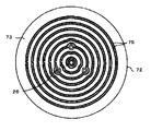
このようなセラミック製のヒータとして、例えば特許文献1や特許文献2には、図7に示すようなセラミック製のヒータが提案されている。
As such a ceramic heater, for example,
このセラミックヒータ71は、板状セラミックスからなる板状体72、金属ケース79、を主要な構成要素としたもので、アルミニウム等の金属からなる有底状の金属ケース79の開口部に、窒化物セラミックスや炭化物セラミックスからなる板状体72を樹脂製の断熱性の接続部材74を介してボルト80で固定され、その上面をウェハWを載せる載置面73とするとともに、板状体72の下面に、例えば図8に示すような同心円状の抵抗発熱体75を備えるようになっていた。
This
さらに、抵抗発熱体75の端子部には、給電端子77がロウ付けされており、この給電端子77が金属ケース79の底部79aに形成されたリード線引出用の孔76に挿通されたリード線78と電気的に接続されるようになっていた。
Furthermore, a
ところで、このようなセラミックヒータ71において、ウェハWの表面全体に均質な膜を形成したり、レジスト膜の加熱反応状態を均質にするためには、ウェハの温度分布を均一にすることが重要である。その為、これまでウェハの面内の温度差を小さくするため、抵抗発熱体75の抵抗分布を調整したり、抵抗発熱体75の温度を分割制御することが行われている。しかし、印刷法で作製した抵抗発熱体は膜厚がばらつき設計通りの抵抗値が得られないとの問題があり、そこで、前記抵抗分布を調整する方法として特許文献2や特許文献4に記載のようなレーザビームで溝を形成して抵抗調整する方法が開示されている。
By the way, in such a
特許文献4のように抵抗発熱体を波状にし、波状部をレーザにてトリミングする方法や、特許文献2に示すように抵抗発熱体の帯にレーザで複数の溝mを形成し、抵抗調整をしたセラミックヒータによりウェハWの温度分布を良くする方法が開示されている。
As described in Patent Document 4, the resistance heating element is corrugated and the corrugated portion is trimmed with a laser, or as shown in
しかし、ウェハ面内の温度差は小さくなるが、ウェハWの表面全体に均質な膜を形成するには未だ不十分であり、温度分布を更に均一に加熱できるようなヒータが求められていた。
ウェハ加熱装置に使用するヒータの抵抗値を調整するためには、レーザー光によるトリミングにより抵抗発熱体の帯の長手方向に溝を形成し、抵抗調整をしてきたが、抵抗調整範囲が大きいと調整しきれないことがあった。 In order to adjust the resistance value of the heater used in the wafer heating device, a groove was formed in the longitudinal direction of the strip of the resistance heating element by trimming with laser light, and the resistance was adjusted. There was something I couldn't do.
また、この抵抗発熱体は、微細に見るとクラックがあり、使用中にクラックが伸展し抵抗増加や断線となるという問題があった。 Further, this resistance heating element has cracks when viewed finely, and there is a problem that the cracks are extended during use, resulting in an increase in resistance and disconnection.
また、それぞれのトリミング加工による抵抗値バラツキが生じ、なかなか狙った抵抗値に加工できないことからウェハWの面内温度差が大きいという問題があった。 Further, there is a problem in that the in-plane temperature difference of the wafer W is large because the resistance value varies due to each trimming process and the resistance value cannot be processed easily.
本発明者は、上記課題について検討した結果、板状体の表面に帯状の抵抗発熱体を備え、該抵抗発熱体の上に、帯の長手方法に略並行で且つ上記帯に直角な方向に連続した複数の溝を有することを特徴とする。 As a result of studying the above problems, the present inventor has provided a strip-shaped resistance heating element on the surface of the plate-like body, and on the resistance heating element, in a direction substantially parallel to the strip longitudinal method and perpendicular to the strip. It has a plurality of continuous grooves.
また、上記抵抗発熱体の帯に直角な方向の断面において、上記複数の溝の表面が滑らかな凹凸面を形成していることを特徴とする。 Further, in the cross section in a direction perpendicular to the band of the resistance heating element, the surfaces of the plurality of grooves form smooth uneven surfaces.
また、上記複数の溝のうち、一部の溝の長さが他と異なることを特徴とする。 In addition, the length of some of the plurality of grooves is different from others.
また、上記複数の溝のうち、外側の溝の長さが他の溝の長さより小さいことを特徴とする。 Further, the length of the outer groove among the plurality of grooves is smaller than the length of the other grooves.
また、上記連続した複数の溝からなる群は、上記抵抗発熱体の帯の長手方向にそって複数に分割され、各群と群との間隔が上記抵抗発熱体の帯の幅よりも小さいことを特徴とする。 The group of the plurality of continuous grooves is divided into a plurality along the longitudinal direction of the band of the resistance heating element, and the distance between each group is smaller than the width of the band of the resistance heating element. It is characterized by.
また、上記溝がレーザー光により形成されたことを特徴とする。 Further, the groove is formed by laser light.
また、上記板状体が炭化物または窒化物を主成分とするセラミックスからなることを特徴とする。 Further, the plate-like body is made of ceramics whose main component is carbide or nitride.
また、レーザー光により溝を形成した後、該溝を形成した抵抗発熱体の抵抗値を測定して、所定の抵抗値と比較し、上記抵抗発熱体が所定の抵抗値となるようにレーザー光により上記溝に沿って新たな溝を形成することを特徴とする。 In addition, after forming the groove by laser light, the resistance value of the resistance heating element having the groove is measured and compared with a predetermined resistance value, so that the resistance heating element has a predetermined resistance value. Thus, a new groove is formed along the groove.
また、抵抗発熱体の両端の抵抗値を測定しながら、レーザー光により溝を形成して上記抵抗値を粗調整する工程と、レーザー光を上記抵抗発熱体に照射しない状態で上記抵抗値を測定する工程と、再度所定の抵抗値となるように上記溝に沿って上記溝より短い溝を形成する工程からなることを特徴とする。 In addition, while measuring the resistance value at both ends of the resistance heating element, a step of forming a groove with a laser beam to roughly adjust the resistance value, and measuring the resistance value without irradiating the resistance heating element with the laser beam And a step of forming a groove shorter than the groove along the groove so as to have a predetermined resistance value again.
また、板状体の一方の主面に複数の抵抗発熱体を備え、他方の主面にウェハを載せる載置面を備え、前記複数の抵抗発熱体に独立して電力を供給する給電部と、該給電部を囲む金属ケースとを備えたことを特徴とする。 A power supply unit that includes a plurality of resistance heating elements on one main surface of the plate-like body, a mounting surface on which the wafer is placed on the other main surface, and that supplies power independently to the plurality of resistance heating elements; And a metal case surrounding the power feeding portion.
本発明の効果として、以下の効果が挙げられる。 The effects of the present invention include the following effects.
基板上に形成された抵抗発熱体の抵抗値を調整するために、レーザー光によるトリミングを実施し、抵抗発熱体の帯の長手方向に略平行で、帯に直角方向に連続した複数の溝を形成することにより、均熱性に優れ、昇降温速度を短縮することが可能となる。 In order to adjust the resistance value of the resistance heating element formed on the substrate, trimming with a laser beam is performed, and a plurality of grooves that are substantially parallel to the longitudinal direction of the band of the resistance heating element and continuous in a direction perpendicular to the band are formed. By forming, it is excellent in soaking | uniform-heating property and it becomes possible to shorten a temperature raising / lowering speed.
また、溝を形成した後に、該溝を形成した抵抗発熱体の抵抗値を測定し、所定の抵抗値と比較するコンパレータを備え、再度所定の抵抗値となるようにレーザー光により上記溝に沿って、更に、断面が滑らかな凹凸面の溝を形成することにより、試料毎のばらつきによる抵抗増加や断線を防止することが可能となる。 In addition, after forming the groove, a resistance value of the resistance heating element having the groove is measured, and a comparator for comparing the resistance value with a predetermined resistance value is provided. Along the groove by laser light so that the predetermined resistance value is obtained again. In addition, by forming a groove with an uneven surface with a smooth cross section, it is possible to prevent an increase in resistance and disconnection due to variations among samples.
また、それぞれのトリミング加工による抵抗値バラツキを最小限に抑えることが可能となる。 In addition, it is possible to minimize the variation in resistance value due to each trimming process.
以下、本発明の実施の形態について説明する。 Hereinafter, embodiments of the present invention will be described.
図1は本発明に係るヒータ1を使ったウェハ加熱装置1の一例を示す断面図であり、炭化珪素、アルミナまたは窒化アルミニウムを主成分とするセラミックスの板状体2の一方の主面を、ウェハWを載せる載置面3とするとともに、他方の主面にガラス又は樹脂等からなる絶縁層4を介して抵抗発熱体5を形成し、該抵抗発熱体5に電気的に接続する給電部6、抵抗発熱体5を冷却するエアーを噴出する噴出口12を具備している。
抵抗発熱体5は、絶縁層4上にスクリーン印刷の手法を用いて形成される。抵抗発熱体5は、導通成分の金属と固着成分のガラスの粉末を適当なバインダー、有機溶剤、分散剤とともに混合、混練する事ことによりペーストが作製され、スクリーン印刷される。スクリーン印刷後、500℃以上で焼成すると安定した抵抗値の抵抗発熱体5を形成できる。
FIG. 1 is a cross-sectional view showing an example of a
The
また、抵抗発熱体5中に含まれる導通成分として、耐熱性および耐酸化性が良好なPt族金属、Au、もしくはこれらの合金を主成分とするものを使用することが好ましい。抵抗発熱体5は、絶縁層4との密着性および抵抗発熱体5自体の焼結性を向上させるために、30〜75重量%のガラス成分を含むことが好ましい。
Moreover, it is preferable to use as a conduction | electrical_connection component contained in the
抵抗発熱体5は、図4に示したような複数の抵抗発熱体に分割され、個々の抵抗発熱体は円弧状のパターンと直線状のパターンとからなる渦巻き状や折り返し形状とすることができる。そして、抵抗発熱体5を複数の抵抗発熱体は、それぞれの温度を独立に制御することにより、広い載置面3を均一に加熱することが好ましい。
The
しかし、スクリーン印刷で形成した抵抗発熱体5は、部分的に厚みや幅が微妙に異なりウェハWの表面温度差を0.4℃以内或いは0.2℃以内に制御するに際し、上記厚みや幅のバラツキにより設計した通りの発熱が得られずウェハW面内の温度差を小さくすることが困難であった。そこで、板状体2の表面に抵抗発熱体5を形成した後、該抵抗発熱体5の帯にレーザー光を照射して、調節する場合、レーザー光により抵抗発熱体5の一部を溝状に除去して抵抗発熱体5の断面積を小さくすることで抵抗発熱体5の帯の一部の抵抗を大きくしてウェハW面内の温度差を小さくすることができる。
However, the
このような方法を用いて抵抗発熱体5の帯の断面積を調整することで、例えば、抵抗発熱体5を形成した際、一部の帯に厚い部分ができたり、全体的に設計値よりも幅が広くなったりした場合等において、抵抗発熱体の断面積を小さくして帯の一部の抵抗値を増大させることにより発熱量を大きくすることができる。そして、抵抗発熱体5の発熱量の制御をより精密に行うことができるため、ウェハW面内の温度差が小さくなるように調製することができる。
By adjusting the cross-sectional area of the band of the
本発明のヒータ1は、板状体2の表面に帯状の抵抗発熱体5を備え、該抵抗発熱体5の上に帯の長手方向に略並行で且つ上記帯に直角な方向に連続した複数の溝14を有することを特徴としている。図2のように、抵抗発熱体5に複数の溝14を並列に形成する事により抵抗調整範囲を効率的に拡げる事ができる。抵抗発熱体5の帯に直角な方向に連続した複数の溝14が形成されていると、溝14同士が幅方向に繋がっていることから帯の幅に対し最大限の抵抗調整ができる。この様に形成されていると抵抗発熱体5の帯の抵抗値を大きく調整することができ、大型のウェハWの面内に対応して板状体2の載置面3に形成された抵抗発熱体5の全面において所定の抵抗値に調整できることから、ウェハWの面内温度差を±0.2℃或いは±0.l℃以内と極めて小さくすることができる。
A
抵抗発熱体5はスクリーン印刷法で形成するのでミクロに見ると厚みや幅のバラツキが存在し、またポーラスな組織となるので、抵抗調整できるレベルまでレーザー光で溝を加工すると、レーザー光で加工した溝14の底部にクラックが発生することがあり、このクラックが絶縁層4や板状体22にまで達し加熱冷却時の熱衝撃により絶縁層4や板状体22にまで達する事になる。特許文献3のようにレーザー加工開始時においてレーザー光照射後にレーザー光の移動を始めた場合やレーザー加工終了時において減速させながら停止させる場合は、溝加工の深さ方向でレーザー光の照射エネルギーが大きくなり、溝が重なる部分で深く形成され、絶縁層4までレーザー光が達し絶縁破壊を生じたり、抵抗発熱体5の溝14の底部から多数のクラック17が生じ、加熱冷却サイクルで大きく抵抗発熱体5の抵抗が変化し、異常発熱、断線へと発展するおそれがある。
Since the
そこで本発明のヒータ1の抵抗発熱体5は、図3に示すように、抵抗発熱体5を形成する帯の長手方向に直角な断面において、複数の溝14の表面が滑らかな凹凸面を形成していることが好ましい。複数の溝14の表面が滑らかな凹凸面を形成していると溝14から抵抗発熱体5へのクラックの伸展や発生を抑制することができて好ましい。しかも溝14の加工による加工歪みから生じる抵抗発熱体5内部の応力を緩和することができ、クラックの伸展や発生を防止することができる。さらに、クラックを防止できる事から、クラック部分で発生する異常発熱を抑制でき、均熱性が向上する。これは、本発明のようにレーザー光により溝14の加工を行う場合、前回の照射箇所と部分的に重なる位置に次の照射が行われるようにすると、溝14間の抵抗発熱体5は溶融し、前回のレーザー加工によって生じたクラックを除去する効果があると考えられる。このような溝14を形成するには、レーザー光の加工出力と加工速度を適正に合わせる必要がある。レーザー光発振器とレーザー光を移動させる可動ミラーを同調させて、レーザーが1回照射された後、前回の照射箇所と部分的に重なる位置に次の照射が行われるように可動ミラーが動き、次のレーザー光を照射するように制御して個々の溝14を形成するとともに複数の溝14が連続するように溝14を形成することが好ましい。
Therefore, as shown in FIG. 3, the
図6の(a)のように溝44と溝44が連続しないで離間していると溝と溝の間に連続した台形状の壁45が発生し、この台形状の壁45にクラックが発生し易くなり、抵抗発熱体5を急速に加熱したり冷却するとこの台形状の壁45が脱落しウェハW面内の温度差が大きくなる虞があり好ましくない。
As shown in FIG. 6A, if the
また、上記連複数の溝14のうち、一部の溝14の長さが他と異なることが好ましい。図4のような大型の板状体2の全面を加熱するような抵抗発熱体5を全面に渡って発熱量を調整するには、抵抗発熱体5を50〜200程の領域に分割し、その分割した領域の抵抗値を所定の値に入るように溝14を形成し、各分割領域の発熱量を調整することでウェハW全面の温度差を小さくするように調整できる。このような分割領域の抵抗値は予め決められた抵抗値になるように溝14を形成するのであるが、各分割領域の両端の抵抗を直接触針を当て測定しながら、溝14を形成するが、レーザ加工しながら抵抗値を測定していることから、レーザ加工している部分の温度が上昇した状態の抵抗値は、その抵抗発熱体5の温度係数にもよるが常温の抵抗値より大きくなることから、所定の抵抗値に調整しても、常温では抵抗値が微妙に異なる虞があった。そこで、抵抗発熱体5の抵抗値を測定しながら溝14を複数形成し、所定の抵抗値に近づいた状態で一旦レーザ光の照射を停止し抵抗発熱体5を常温に冷した後、抵抗発熱体5の抵抗値を測定し所定の抵抗値と比較し最後の溝14を形成することで、各領域の抵抗値を精度良く調整することができる。そして、各領域に形成する複数の溝14の最後に形成する溝14は他の溝14より長さを短くすることで、領域の抵抗値を更に微妙に調整することができることからウェハWの表面温度差をより小さくすることができて好ましい。更に、各領域の抵抗値を調整するには他より短い溝14を形成し抵抗調整した後再度レーザ光の照射を止めて、抵抗発熱体5の温度を常温に戻した状態で抵抗を測定し更に微細な抵抗調整するための所定の長さの溝14を形成することが好ましい。このように各領域の抵抗値を調整することで各領域の抵抗値を細かく調整することが可能となり、ウェハWの面内温度差を小さくすることができて好ましい。
Moreover, it is preferable that the length of some of the
また、連続した複数の溝14の外側の溝14の長さが他の溝14の長さより小さいことが好ましい。その理由は、溝14は帯の中心に形成することが抵抗発熱体5の全体の対称性が変化する虞が少なく好ましい。そしてこのような溝14は帯の中心に最初の溝14を形成しその外側に左右順番に形成されるが、最後の溝14は他の溝14より短くその外側に形成されることで、微細な抵抗調整を達成することができるからである。
Moreover, it is preferable that the length of the
また、上記連続した複数の溝14からなる群G1、G2・・・は、上記抵抗発熱体5の帯の長手方向に沿って複数に分割され、各郡Gと群Gとの間隔が上記抵抗発熱体の帯の幅よりも小さいことが好ましい。例えば、上記群G1と群G2との間隔が前記帯の幅より小さいことが好ましい。抵抗発熱体5を50〜200個に分割した各領域において、群G1と群G2との間隔が帯の幅より小さいと、群G1と群G2との間にクールスポットが発生する虞がなく好ましい。また、領域内で群G1と群G2に分割することで領域内の抵抗値を分散して調整することができ、領域内の温度バラツキを小さくすることができて好ましい。
The groups G1, G2,... Composed of the plurality of
また、本発明の板状体2は、炭化物または窒化物を主成分とするセラミックスからなることが好ましい。このような板状体2はヤング率が300GPa以上と大きく熱を加えても変形が小さく、板状体2の厚を2〜4mm以下と薄くできるため、所定の処理温度に加熱するまでの昇温時間及び所定の処理温度から室温付近に冷却するまでの冷却時間を短くすることができ、半導体製造装置としての生産性を高めることができる。また、板状体2としてより好ましくは炭化珪素室焼結体または窒化アルミニウム質焼結体、炭化ホウ素質焼結体、窒化珪素質焼結体を用いることが好ましく、板状体2の熱伝導率を150〜250W/(m/K)と大きくすることができることから、ウェハW表面の温度差を小さくすることが容易となり好ましい。
Moreover, it is preferable that the plate-
次に、本発明のヒータ1の製造方法について説明する。
Next, the manufacturing method of the
本発明のヒータ1は、レーザー光により溝14を形成した後、該溝14を形成した抵抗発熱体5の抵抗値を測定して、所定の抵抗値と比較し、上記抵抗発熱体が所定の抵抗値となるようにレーザー光により上記溝14に沿って新たな溝14を形成することが好ましい。レーザー光により溝14を形成した抵抗発熱体5の抵抗値を測定し、所定の抵抗値と比較するコンパレータを備え、所定の抵抗値となるようにレーザー光により上記溝14に沿って新たな溝14を形成することが好ましい。このようにレーザー光により溝14を形成した抵抗発熱体5の抵抗値を測定し、その抵抗値をコンパレータで比較し所定の抵抗値となっていなければ、再度所定の抵抗値となるようにレーザー光により上記溝14に沿って新たな溝14を形成することで各領域の抵抗値を所定の抵抗値に入れることができることから、ウェハW面内の温度差をより小さくすることができて好ましい。
In the
また、抵抗発熱体5の両端の抵抗値を測定しながら、レーザー光により溝を形成して上記抵抗値を粗調整する工程と、レーザー光を上記抵抗発熱体5に照射しない状態で上記抵抗値を測定する工程と、再度所定の抵抗値となるように上記溝14に沿って上記溝14より短い溝14を形成する工程からなることが好ましい。抵抗発熱体5の両端の抵抗値を測定しながら、所定の抵抗値となるように溝14を連続して形成すると短時間で溝14を加工することができて好ましい。しかし、レーザ光を照射しながら抵抗測定を行うと抵抗発熱体の一部が加熱されていることから抵抗発熱体5の抵抗が大きく測定される虞があり正確な精度で抵抗調整することができない。そこで、より微細に正確に抵抗調整するにはレーザ照射を止めて、溝14を形成した後に抵抗発熱体5の抵抗値を測定することが重要であり、しかもこの抵抗値は常温で測定することが重要である。先に述べたようにレーザ光を照射した状態では抵抗発熱体の温度が部分的に高くなっていることから測定抵抗値が大きくなる虞があり、正確な抵抗値を測定することが困難であるが、レーザ光の照射を止め、抵抗発熱体5の温度を常温にして抵抗を測定することでより正確な抵抗値を求めることができる。因みにこのレーザ光の照射を停止する時間は100m秒程度あれば抵抗発熱体5の温度は常温に戻ることができて、正確な抵抗値を測定することができる。そして、この正確な抵抗値に基づき溝14の長さを短く調整した溝14を形成することで微小な抵抗調整を実施することができる。
In addition, while measuring the resistance value at both ends of the
次に、本発明の抵抗発熱体のレーザ光によるトリミング工程についてより詳細に説明する。 Next, the trimming process by the laser beam of the resistance heating element of the present invention will be described in more detail.
レーザー光による加工量は出力と加工部分の照射時間の積で決まるものであり、加工速度を変えると総体的に加工量が変動する。ちなみに、この溝14の加工は、レーザー光波長が1.06μmのYAGレーザー光を用い、トリミング速度を5〜20mm/secに設定して実施したものである。出力は、約0.5W、スポット径は約60μmである。
レーザー光による加工において、絶縁層4上の抵抗発熱体5を加工する様な場合、レーザー光の出力を調整し、形成した溝14の深さは抵抗発熱体5の厚みの2/3程度とすることが望ましい。例えば、抵抗発熱体5を完全に貫通するようにレーザー出力を調整すると、抵抗発熱体5には厚みのばらつきがある為、抵抗発熱体5の厚みの薄い箇所では、絶縁層4までレーザー光が到達し絶縁層4が絶縁破壊を起こすおそれがある。また、抵抗発熱体5を厚み方向に浅く溝14を加工する様にレーザー出力を調整すると、レーザー加工で調整できる抵抗値の範囲が小さくなり、加工する溝14の本数が増し、レーザー加工工程にかかる時間が長くなり、作業効率が悪くなる。
The processing amount by the laser light is determined by the product of the output and the irradiation time of the processing portion. When the processing speed is changed, the processing amount generally varies. Incidentally, the processing of the
When processing the
本発明でのレーザートリミングは、予め、帯状の抵抗発熱体5を所定の長さ毎に4端子法で抵抗値を測定し、目標とする抵抗値との差を演算し求める。求められた差を部位毎にレーザートリミング装置へ入力する。図5に示す様に可動ミラー29を備えたレーザー光発振器25と、帯状の抵抗発熱体5を備えた板状体2を載せる為の可動テーブルを備え、レーザー光発振器から発したレーザー光を抵抗発熱体5の帯に目標とする抵抗値との差分照射し、上記溝14を形成する工程において、固定テーブルに可動ミラー29を介して、レーザー光を照射して帯状の溝14を形成することができる。レーザー光の波長が1.06μmのYAGレーザー光を用い、スポット径は約60μmである。本発明のレーザー加工においては、事前に、1ポイントに照射できる照射時間、つまり、パルスの回数を規定しておく。これは、前述したように抵抗発熱体5を貫通し、絶縁層2を破壊しないようなパワーにレーザー加工条件として設定する必要がある為である。ここで、レーザーの照射時間、出力、可動ミラー29のタイミングがずれると、長時間1箇所にレーザー光が照射され、溝14の底面の周辺に多数のクラックが生じたり、または、レーザー光を照射しながら移動するため溝加工底面が深く鋭角となる場合が生じる。また、抵抗発熱体5の構成成分が変われば、この加工条件も変更となる。ここで、レーザー光発振器25のパルスレーザー光と可動ミラー29の回転が同期しており、レーザー光が1回照射された後、前回加工場所と部分的に重なる場所に照射するように可動ミラー15が動き、次のレーザーを照射するように制御されていることが好ましい。
In the laser trimming according to the present invention, the resistance value of the belt-like
レーザーの加工位置と加工する長さは事前に、X、Y軸の座標データ、進行角度データ、距離データとして登録されており、板状体2を可動テーブル34の上に置き、不図の位置合わせ用ポイントの座標をカメラ26で読みとり、加工開始位置/停止位置を決定する。
The laser processing position and processing length are registered in advance as coordinate data for the X and Y axes, travel angle data, and distance data. The plate-
レーザー光発振器25から発振されたレーザー光は、加工位置に照射される様に制御された可動ミラー29を介して、板状体2上の抵抗発熱体5に溝14を加工する。可動ミラーを介して照射されるレーザー光の到達距離から、加工面積は制限されるため、可動テーブル34上で図4に示す板状体2を順次移動させ、板状体2上の抵抗発熱体5の帯の全体に溝14を加工し、抵抗値を調整することができる。つまり、目標とする抵抗値との差に基づき、抵抗値を測定しながら、レーザー光を照射し所定の長さ毎に、抵抗発熱体を切り上げ、複数の溝を形成し、所定の抵抗値となるまで再度、複数回抵抗値の調整が行われる為、本発明のヒータ1は、連続した複数の溝の一部の溝の長さが異なることを特徴としており、且つ、この連続した複数の溝の外側の溝の長さが他の溝の長さより短く小さいことを特徴としているように、加工と測定による確認を繰り返す為、抵抗値バラツキの積算を最小限に押さえることが可能となる。
The
抵抗調整された板状体2は洗浄後、他部品と合わせてヒータ1へと組み立てられる。板状体2全体の温度が、1分間で350℃となるような電圧を印加し、3分間保持した後、6kg/mm3、80L/minのエアーにて、2分で40℃以下に強制冷却する冷熱サイクルを5000サイクルかけて、その前後の溝14を施した帯の部分の抵抗値変化を調査した。そのときの抵抗変化が初期値と比較し、5%以内のものは実用に耐えるが、5%を越えるものは実用的でない。抵抗変化が5%を越えると、局所発熱が発生し、ヒータ1の均熱が崩れる。また、抵抗発熱体5の抵抗値の変化により、ヒータの出力のバランスが崩れるうえ、ウェハWが載置される場合、ウェハWの加熱にムラが生じることとなる。
The plate-
次に、本発明のその他の構成について詳細を説明する。 Next, details of other configurations of the present invention will be described.
板状体2を形成する炭化珪素質焼結体は、主成分の炭化珪素に対し、焼結助剤として硼素(B)と炭素(C)を添加したり、もしくはアルミナ(Al2O3)、イットリア(Y2O3)のような金属酸化物を添加して十分混合し、平板状に加工したのち、1900〜2100℃で焼成することにより得られる。炭化珪素はα型を主体とするものあるいはβ型を主体とするもののいずれであっても構わない。
In the silicon carbide sintered body forming the plate-
また、炭化硼素質焼結体としては、主成分の炭化硼素に対し、焼結助剤として炭素を3〜10重量%混合し、2000〜2200℃でホットプレス焼成することにより焼結体を得ることができる。 The boron carbide sintered body is obtained by mixing 3 to 10% by weight of carbon as a sintering aid with boron carbide as a main component, and performing hot press firing at 2000 to 2200 ° C. be able to.
そして、窒化硼素質焼結体としては、主成分の窒化硼素に対し、焼結助剤として30〜45重量%の窒化アルミニウムと5〜10重量%の希土類元素酸化物を混合し、1900〜2100℃でホットプレス焼成することにより焼結体を得ることができる。 In the boron nitride sintered body, 30 to 45% by weight of aluminum nitride and 5 to 10% by weight of rare earth element oxide are mixed as a sintering aid with respect to boron nitride as a main component, and 1900 to 2100. A sintered body can be obtained by hot-press firing at ° C.
また、炭化硼素質焼結体としては、主成分の炭化硼素に対し、焼結助剤として炭素を3〜10重量%混合し、2100〜2200℃でホットプレス焼成することにより焼結体を得ることができる。 The boron carbide sintered body is obtained by mixing 3 to 10% by weight of carbon as a sintering aid with boron carbide as a main component, and performing hot press firing at 2100 to 2200 ° C. be able to.
また、板状体2を形成する窒化アルミニウム質焼結体は、主成分の窒化アルミニウムに対し、焼結助剤としてY2O3やYb2O3等の希土類元素酸化物と必要に応じてCaO等のアルカリ土類金属酸化物を添加して十分混合し、平板状に加工した後、窒素ガス中1900〜2100℃で焼成することにより得られる。
Further, the aluminum nitride sintered body forming the plate-
また、板状体2を形成する窒化珪素質焼結体としては、主成分の窒化珪素に対し、焼結助剤として3〜12重量%の希土類元素酸化物と0.5〜3重量%のAl2O3、さらに焼結体に含まれるSiO2量として1.5〜5重量%となるようにSiO2を混合し、1650〜1750℃でホットプレス焼成することにより焼結体を得ることができる。ここで示すSiO2量とは、窒化珪素原料中に含まれる不純物酸素から生成するSiO2と、他の添加物に含まれる不純物としてのSiO2と、雰囲気からの影響を含め意図的に添加したSiO2の総和である。
The silicon nitride-based sintered body forming the plate-
一方、炭化珪素質焼結体を板状体2として使用する場合、半導電性を有する板状体2と抵抗発熱体5との間の絶縁を保つ絶縁層4としては、ガラス又は樹脂を用いることが可能である。ここで、ガラスを用いる場合、その厚みが100μm未満では耐電圧が1.5kVを下回り絶縁性が保てず、逆に厚みが600μmを越えると、板状体22を形成する炭化珪素質焼結体との熱膨張差が大きくなり過ぎるために、クラックが発生して絶縁層4として機能しなくなる。その為、絶縁層4としてガラスを用いる場合、絶縁層4の厚みは100μm〜600μmの範囲で形成することが好ましく、望ましくは200μm〜350μmの範囲で形成することが良い。
On the other hand, when a silicon carbide sintered body is used as the plate-
また、板状体2を窒化アルミニウムを主成分とするセラミック焼結体で形成する場合は、板状体22に対する抵抗発熱体5の密着性を向上させるために、ガラスからなる絶縁層4を形成する。ただし、抵抗発熱体5の中に十分なガラスを添加し、これにより十分な密着強度が得られる場合は、省略することが可能である。
When the plate-
この絶縁層4を形成するガラスの特性としては、結晶質又は非晶質のいずれでも良く、耐熱温度が300℃以上でかつ0℃〜300℃の温度域における熱膨張係数が板状体22を構成するセラミックスの熱膨張係数に対し−5〜+5×10⁷/℃の範囲にあるものを適宜選択して用いることが好ましい。即ち、熱膨張係数が前記範囲を外れたガラスを用いると、板状体22を形成するセラミックスとの熱膨張差が大きくなりすぎるため、ガラスの焼付け後の冷却時においてクラックや剥離等の欠陥が生じ易いからである。
The glass forming the insulating layer 4 may be crystalline or amorphous, and has a heat expansion coefficient of 300 ° C. or higher and a thermal expansion coefficient in the temperature range of 0 ° C. to 300 ° C. It is preferable to select and use one having a thermal expansion coefficient in the range of −5 to + 5 × 10 7 / ° C. as appropriate. That is, if a glass having a thermal expansion coefficient outside the above range is used, the difference in thermal expansion from the ceramic forming the plate-
絶縁層4をガラスで形成する場合、ガラス粉末を適当なバインダー、分散材、有機溶剤と混合、混練することでペーストを作成し、利用する事が望ましい。 When the insulating layer 4 is formed of glass, it is desirable to prepare and use a paste by mixing and kneading glass powder with an appropriate binder, dispersion material, and organic solvent.
次に、絶縁層4に樹脂を用いる場合、その厚みが30μm未満では、耐電圧が1.5kVを下回り、絶縁性が保てなくなるとともに、抵抗発熱体5にレーザー光で溝14を形成した際に絶縁層4を傷付けるおそれがあり、該傷により絶縁層4として機能しなくなる。逆に厚みが150μmを越えると、樹脂の焼付け時に発生する溶剤や水分の蒸発量が多くなり、板状体22との間にフクレと呼ばれる泡状の剥離部ができ、この剥離部の存在により熱伝達が悪くなるため、載置面3の均熱化が阻害される。その為、絶縁層4として樹脂を用いる場合、絶縁層4の厚みは30μm〜150μmの範囲で形成することが好ましく、望ましくは60μm〜150μmの範囲で形成することが良い。
Next, when a resin is used for the insulating layer 4, if the thickness is less than 30 μm, the withstand voltage is less than 1.5 kV and the insulation cannot be maintained, and the
また、絶縁層4を樹脂により形成する場合、300℃以上の耐熱性と抵抗発熱体5との密着性を考慮すると、ポリイミド樹脂、ポリイミドアミド樹脂、ポリアミド樹脂等を用いることが好ましい。
In addition, when the insulating layer 4 is formed of a resin, it is preferable to use a polyimide resin, a polyimide amide resin, a polyamide resin, or the like in consideration of heat resistance of 300 ° C. or more and adhesion between the
なお、ガラスや樹脂からなる絶縁層4を板状体22上に被着する手段としては、前記ガラスペースト又は樹脂ペーストを板状体22の中心部に適量落とし、スピンコーティング法にて伸ばして均一に塗布するか、あるいはスクリーン印刷法、ディッピング法、スプレーコーティング法等にて均一に塗布したあと、ガラスペーストの場合は800℃の温度で、樹脂ペーストの場合は400℃以上の温度で焼き付ければ良い。また、絶縁層4としてガラスを用いる場合、予め炭化珪素質焼結体又は窒化アルミニウム質焼結体からなる板状体22を1200℃程度の温度に加熱し、絶縁層4を被着する表面を酸化処理しておくことで、ガラスからなる絶縁層4との密着性を高めることができる。
In addition, as means for depositing the insulating layer 4 made of glass or resin on the plate-
また、図1に示すように、給電部6と導通端子7の接続手段を弾性体8による押圧としている為、板状体22と支持体11の温度差による両者の膨張の差を接触部分の滑りで緩和できるので、使用中の熱サイクルに対し良好なウェハ加熱装置1とすることができる。
Further, as shown in FIG. 1, since the connecting means between the power feeding unit 6 and the conduction terminal 7 is pressed by the elastic body 8, the difference in expansion between the plate-
この押圧手段である弾性体8としては、図1に示すようなコイル状のバネや、他に板バネ等を用いて押圧するようにしても構わない。これらの弾性体8の押圧力としては、0.3N以上の荷重を導通端子7に掛けるようにすればよい。弾性体8の押圧力を0.3N以上とする理由は、板状体2および支持体11の膨張収縮による寸法変化に対し、それに応じて導通端子7が移動しなければならないが、装置の構成上導通端子7を板状体2の下面から給電部6に押し当てるようにしているため、導通端子7の摺動部との摩擦により導通端子7が給電部6から離れることを防止する為である。
As the elastic body 8 as the pressing means, a coiled spring as shown in FIG. 1 or a plate spring or the like may be used for pressing. The pressing force of these elastic bodies 8 may be such that a load of 0.3 N or more is applied to the conduction terminal 7. The reason why the pressing force of the elastic body 8 is 0.3 N or more is that the conduction terminal 7 must move in response to the dimensional change caused by the expansion and contraction of the plate-
また、導通端子7の給電部6との当接面側の径は、1.5〜4mmとすることが好ましい。さらに、導通端子7を保持する絶縁材9は、その使用温度に応じて、200℃以下の温度では、ガラス繊維を分散させたPEEK(ポリエトキシエトキシケトン樹脂)材のものを用いることが可能であり、また、それ以上の温度で使用する場合は、アルミナ、ムライト等からなるセラミック製の絶縁材9を用いることが可能である。 Moreover, it is preferable that the diameter of the contact surface side with the electric power feeding part 6 of the conduction terminal 7 shall be 1.5-4 mm. Furthermore, as the insulating material 9 for holding the conductive terminal 7, a PEEK (polyethoxyethoxyketone resin) material in which glass fibers are dispersed can be used at a temperature of 200 ° C. or lower depending on the use temperature. In addition, when used at a temperature higher than that, it is possible to use a ceramic insulating material 9 made of alumina, mullite or the like.
このとき、導通端子7の少なくとも給電部6との当接部を、Ni、Cr、Ag、Au、ステンレスおよび白金族の金属のうち少なくとも1種以上からなる金属により形成することが好ましい。具体的には、導通端子7自体を上記金属で形成するか、または導通端子7の表面に該金属からなる被覆層を設けることもできる。また、導通端子7と給電部6の間に上記金属からなる金属箔を挿入することにより、導通端子7表面の酸化による接触不良を防止し、板状体22の耐久性を向上させることが可能である。具体的には、前記給電部6と導通端子7の間に、Ni、Cr、Ag、Au、ステンレスおよび白金族の金属うち少なくとも1種以上からなる金属箔16を挿入すると、電気的な接触の信頼性が増すと同時に、板状体22と支持体11の温度差に起因する寸法差を金属箔の面の滑りで緩和できる。
At this time, it is preferable that at least the contact portion of the conduction terminal 7 with the power feeding portion 6 is formed of a metal composed of at least one of Ni, Cr, Ag, Au, stainless steel, and platinum group metals. Specifically, the conductive terminal 7 itself can be formed of the above metal, or a coating layer made of the metal can be provided on the surface of the conductive terminal 7. Further, by inserting a metal foil made of the above metal between the conductive terminal 7 and the power feeding portion 6, it is possible to prevent contact failure due to oxidation of the surface of the conductive terminal 7 and improve the durability of the plate-
また、導通端子7の表面にブレーチング加工やサンドブラスト加工を施したりして、表面を荒らすことにより接点が点接触となることを防止すると、さらに接触の信頼性を向上させることができる。 Further, if the surface of the conductive terminal 7 is subjected to brazing or sandblasting to prevent the contact from becoming a point contact by roughening the surface, the contact reliability can be further improved.
なお、板状体2は金属製のケース11に、その開口部を覆うように設置してある。金属製のケース11は、側壁部と一層もしくは多層の板状構造部13を有している。また該板状構造部13には、板状体22の抵抗発熱体5に給電するための給電部6と導通するための導通端子7が絶縁材9を介して設置され、弾性体8により板状体22の表面の給電部6に押圧されている。また、熱電対10は、板状体2の載置面3の直近に設置され、熱電対10の温度を基に板状体22の温度を調整する。また、抵抗発熱体5が複数のブロックに別れており、個別に温度制御する場合は、それぞれの抵抗発熱体5のブロックに測温用の熱電対10を設置する。この抵抗発熱体5は、複数の溝を有し、溝がレーザー光により形成されたことを特徴としている為、抵抗調整されたヒータ複数により構成され、より均熱性の高いウェハ加熱装置といえる。
The plate-
また、板状体2には、冷却するためにエアー噴出口12、およびガスを排気するための不図示の開口部を形成することで、昇降温速度にも優れる。このように板状体2の冷却機構を設けることにより、ウェハWの表面に半導体薄膜やレジスト膜を形成したり、表面をエッチングしたりするウェハ加熱装置を構成することができる。
In addition, the plate-
また、支持体7内に昇降自在に設置された不図示のリフトピンにより、ウェハWを載置面3上に載せたり載置面3より持ち上げたりといった作業がなされる。そして、ウェハWは、不図示のウェハ支持ピンにより載置面3から浮かした状態で保持され、片当たり等による温度バラツキを防止するようにしている。 In addition, work such as placing the wafer W on the placement surface 3 or lifting it from the placement surface 3 is performed by lift pins (not shown) installed in the support 7 so as to be movable up and down. The wafer W is held in a state of being lifted from the mounting surface 3 by a wafer support pin (not shown) so as to prevent temperature variations due to contact with each other.
そして、このウェハ加熱装置1によりウェハWを加熱するには、不図示の搬送アームにて載置面3の上方まで運ばれたウェハWを不図示のリフトピンにて支持したあと、リフトピンを降下させてウェハWを載置面3上に載せる。
In order to heat the wafer W by the
また、板状体2の温度は、板状体2にその先端が埋め込まれた熱電対10により測定する。熱電対10としては、その応答性と保持の作業性の観点から、外径1.0mm以下のシース型の熱電対10を使用することが好ましい。また、板状体2に埋め込まれた先端部に力が掛からないように熱電対10の途中が支持部7の板状構造部13に保持されている。この熱電対10の先端部は、板状体2に孔が形成され、この中に設置された円筒状の金属体の内壁面にバネ材により押圧固定することが測温の信頼性を向上させるために好ましい。
Further, the temperature of the plate-
さらに、これらのウェハ加熱装置1をレジスト膜形成用として使用する場合は、板状体2として窒化物を主成分とする材料を使用すると、大気中の水分等と反応してアンモニアガスを発生させレジスト膜を劣化させるため、この場合板状体2として、炭化珪素や炭化硼素等の炭化物からなるものを使用することが好ましい。また、この際、焼結助剤に水と反応してアンモニアやアミンを形成する可能性のある窒化物を含まないようにすることが必要である。
Further, when these
炭化物または窒化物等のセラミックスを用い、抵抗発熱体を同心円状に分割形成した複数のパターンをレーザー光により溝を形成するトリミングにより抵抗調整し、これに通電することにより加熱するセラミックヒータを使用したウェハ加熱装置を搭載した半導体製造装置は、レジストの加熱・乾燥等の処理時間が短く、加熱温度精度の向上、ウェハ処理時間の短縮を達成し、装置のランニングコスト低減を実現し、ウェハW上に微細な配線を高密度に形成することが可能となる。 Using ceramics such as carbides or nitrides, a ceramic heater is used that adjusts the resistance by trimming the grooves formed by concentrically dividing the resistance heating element by laser light, and heats it by energizing it. Semiconductor manufacturing equipment equipped with a wafer heating device shortens the processing time for resist heating and drying, improves the heating temperature accuracy, shortens the wafer processing time, reduces the running cost of the device, and on the wafer W In addition, fine wiring can be formed with high density.
熱伝導率が80W/(m・K)の炭化珪素質焼結体に研削加工を施し、板厚3mm、外径300mmの円板状をした板状体を複数作製し、各板状体の一方の主面に絶縁層を被着するため、ガラス粉末に対してバインダーとしてのエチルセルロースと有機溶剤としてのテルピネオールを混練して作製したガラスペーストをスクリーン印刷法にて敷設し、150℃に加熱して有機溶剤を乾燥させた後、550℃で30分間脱脂処理を施し、さらに700〜900℃の温度で焼付けを行うことにより、ガラスからなる厚み200μmの絶縁層を形成した。次いで絶縁層上に抵抗発熱体を被着させるため、導電材として20重量%のAu粉末と10重量%のPt粉末と70重量%のガラスを所定量のパターン形状に印刷した後、150℃に加熱して有機溶剤を乾燥させ、さらに450℃で30分間脱脂処理を施した後、500〜700℃の温度で焼付けを行うことにより、厚みが50μmの抵抗発熱体を形成した。抵抗発熱体は、中心部と外周部を周方向に4分割した5パターン構成とした。 A silicon carbide sintered body having a thermal conductivity of 80 W / (m · K) is ground to produce a plurality of plate-like bodies each having a plate thickness of 3 mm and an outer diameter of 300 mm. In order to deposit an insulating layer on one main surface, a glass paste prepared by kneading ethyl cellulose as a binder and terpineol as an organic solvent into glass powder was laid by screen printing and heated to 150 ° C. After drying the organic solvent, degreasing treatment was performed at 550 ° C. for 30 minutes, and baking was performed at a temperature of 700 to 900 ° C. to form an insulating layer made of glass having a thickness of 200 μm. Next, in order to deposit a resistance heating element on the insulating layer, 20% by weight of Au powder, 10% by weight of Pt powder and 70% by weight of glass as a conductive material are printed in a predetermined pattern shape, and then heated to 150 ° C. The organic solvent was dried by heating, and after degreasing at 450 ° C. for 30 minutes, baking was performed at a temperature of 500 to 700 ° C. to form a resistance heating element having a thickness of 50 μm. The resistance heating element has a five-pattern configuration in which the central portion and the outer peripheral portion are divided into four in the circumferential direction.
こうして作製した抵抗発熱体の各パターンをそれぞれ帯の長手方向に50箇所前後に分割し、各箇所で設計した抵抗値と実測抵抗値とを4端子測定法で測定し、その差分をレーザビームを照射して溝を形成して抵抗調整した。前記溝の形成方法としては日本電気製のYAGレーザーを使用した。レーザー光は、波長が1.06μm、パルス周波数1KHz、レーザ出力値0.5W、加工速度8mm/sec.として照射した。 Each pattern of the resistance heating element thus produced is divided into about 50 locations in the longitudinal direction of the belt, and the resistance value and the measured resistance value designed at each location are measured by a four-terminal measurement method. Irradiation formed grooves to adjust the resistance. As a method for forming the groove, a YAG laser manufactured by NEC was used. The laser beam has a wavelength of 1.06 μm, a pulse frequency of 1 KHz, a laser output value of 0.5 W, a processing speed of 8 mm / sec. As irradiated.
尚、上記条件で作製された溝の幅は約60μmで深さは約20μmであった。そして、各群毎に形成された溝と溝との間隔であるピッチは約50μmで最大の溝の数は13個であった。 The width of the groove produced under the above conditions was about 60 μm and the depth was about 20 μm. And the pitch which is the space | interval of the groove | channel formed for every group was about 50 micrometers, and the number of the largest groove | channels was 13.
ここで、レーザー光の重なり状態を変え、複数溝を形成した後に、抵抗値を測定し、所定の抵抗値と比較し、再度所定の抵抗値となるように複数回、レーザー光により上記溝に沿って外側へ、他の溝より長さが小さく異なる試料を作製した。 Here, after changing the overlapping state of the laser light and forming a plurality of grooves, the resistance value is measured, compared with a predetermined resistance value, and again in the groove by laser light several times so as to become a predetermined resistance value again. A sample having a length smaller than that of the other grooves and different from the other grooves was produced.
抵抗発熱体の両端の抵抗値を測定しながら、所定の抵抗値となるようにレーザー光により溝を形成し、レーザー光により形成された溝がそれぞれ離れ、重ならない試料をNo.5、6とした。 While measuring the resistance values at both ends of the resistance heating element, grooves were formed by laser light so as to have a predetermined resistance value. 5 and 6.
また、抵抗発熱体の両端の抵抗値を測定しながら、所定の抵抗値となるようにレーザー光により溝を形成し、レーザー光により形成された溝が帯に直角な方向に連続した試料をNo.3、4とした。 In addition, while measuring the resistance value at both ends of the resistance heating element, a groove is formed by laser light so that a predetermined resistance value is obtained, and a sample in which the groove formed by laser light is continuous in a direction perpendicular to the belt is No. . 3 and 4.
更に、帯に直角な方向に連続した溝を形成した後、レーザー光を上記抵抗発熱体に照射しない状態で再度、上記抵抗値を測定し、所定の抵抗値となるようにレーザー光により再度上記溝に沿って上記溝より短い溝を形成した試料をNo.1、2とした。 Further, after forming a continuous groove in a direction perpendicular to the belt, the resistance value is measured again without irradiating the resistance heating element with laser light, and the above-mentioned resistance value is again measured with laser light so as to obtain a predetermined resistance value. A sample in which a groove shorter than the groove was formed along the groove. 1 and 2.
上記抵抗発熱体を形成した板状体を金属ケースに取り付け、測温素子や給電端子等を取り付け、半導体製造装置に用いられるウェハ加熱装置を完成した。 A plate-like body on which the resistance heating element was formed was attached to a metal case, a temperature measuring element, a power supply terminal, and the like were attached to complete a wafer heating apparatus used in a semiconductor manufacturing apparatus.
その後、測温素子付きのウェハを載置面に載せてセラミックヒータを加熱し、ウェハ全体の温度の平均が250℃になるようにして、前記の測温素子付きのウェハを用いてウェハ表面の温度ばらつきと設計した抵抗値との差を測定した。 After that, a wafer with a temperature measuring element is placed on the mounting surface, the ceramic heater is heated, and the average temperature of the entire wafer is 250 ° C. The difference between the temperature variation and the designed resistance value was measured.
さらに、板状体の全体の温度が1分間で350℃となるような電圧を印加し3分間保持した後、6kg/mm3、80L/minのエアーにて、2分で40℃以下に強制冷却する冷熱サイクルを5000サイクルかけて、その前後で溝を施した部分の抵抗値の変化を調査する耐久評価を行った。 抵抗値の測定は、4端子法により接触抵抗を考慮できるようにして測定した。また、評価基準として、上記の耐久テストにおいて、分割された抵抗発熱体5の全抵抗値の抵抗変化率の最大値が5%以内のものは実用的に使えると判断した。また、5%を越えるものは実用的に使えないと判断した。
Furthermore, after applying a voltage such that the entire temperature of the plate-like body becomes 350 ° C. in 1 minute and holding it for 3 minutes, it is forced to 40 ° C. or less in 2 minutes with air of 6 kg / mm 3 and 80 L / min. Endurance evaluation was conducted by investigating changes in resistance values of the grooved portions before and after the cooling cycle of cooling for 5000 cycles. The resistance value was measured by considering the contact resistance by a four-terminal method. In addition, as an evaluation standard, in the above-described durability test, it was determined that the maximum resistance change rate of all resistance values of the divided
それぞれの結果は表1に示すとおりである。

表1に示すように、レーザー光により作製したそれぞれの溝が略並行に離れて形成された試料No.5、6は、ウエハ面内温度差が±0.32℃、±0.36℃と大きく、しかも耐久試験後の抵抗変化率は8.3%、12.4%と大きく好ましくなかった。 As shown in Table 1, sample Nos. 5 and 6 in which the grooves formed by the laser beam are separated substantially in parallel have a difference in temperature in the wafer plane of ± 0.32 ° C. and ± 0.36 ° C. Further, the resistance change rate after the durability test was not preferable because it was 8.3% and 12.4%.
これに対し、本発明の板状体の表面に帯状の抵抗発熱体を備え、該抵抗発熱体の上に、帯の長手方法に略並行で且つ上記帯に直角な方向に連続した複数の溝を有する試料No.1〜4はウェハW面内の温度差が±0.18℃以内と小さく耐久試験後の抵抗変化率1.8%以下と小さく優れた特性を示すことが分った。 On the other hand, a strip-like resistance heating element is provided on the surface of the plate-like body of the present invention, and a plurality of grooves are provided on the resistance heating element in a direction substantially parallel to the band length method and perpendicular to the band. Sample No. having Nos. 1 to 4 show that the temperature difference within the wafer W surface is as small as ± 0.18 ° C. and the resistance change rate after the endurance test is 1.8% or less and exhibits excellent characteristics.
また、抵抗値を測定しながらレーザ光で溝を形成し抵抗値を調整した後、レーザ光の照射を止めてから抵抗値を測定し所定の抵抗値と比較し、再度所定の抵抗値となるようにレーザー光により上記溝に沿って、他の溝より長さが小さい溝を形成した本発明の試料No.1,2は、ウエハ面内温度差が±0.08℃、0.10℃で、耐久試験後の抵抗変化率は0.24%、0.42%となり、試料No.3、4と比較し、更に良好な特性を示した。 Also, after measuring the resistance value and adjusting the resistance value by forming a groove with laser light, the resistance value is measured after stopping the laser light irradiation, and compared with the predetermined resistance value, and again becomes the predetermined resistance value. As described above, the sample No. of the present invention in which a groove having a length shorter than the other grooves is formed along the groove by the laser beam. 1 and 2, the wafer surface temperature difference is ± 0.08 ° C and 0.10 ° C, and the resistance change rate after the durability test is 0.24% and 0.42%. In addition, even better characteristics were exhibited.
1.ヒータ、ウェハ加熱装置
2.板状体
3.載置面
4.絶縁層
5.抵抗発熱体
6.給電部
7.導通端子
8.弾性体
9.絶縁材
10.熱電対
11.支持体
12.エアー噴出口
13.板状構造部
14.溝加工凹部
15.溝加工端断面
16.保護層
20.入力部
21.演算部
22.記憶部
23.制御部
24.抵抗測定部
25.レーザー光発振器
26.カメラ
27.ガルバノメーター
28.レーザー光
29.可動ミラー
30.測定端子
31.板状体
32.ストッパー
33.載物台
34.可動テーブル
1. 1. Heater,
Claims (10)
Priority Applications (5)
| Application Number | Priority Date | Filing Date | Title |
|---|---|---|---|
| JP2004235515A JP2006054125A (en) | 2004-08-12 | 2004-08-12 | Heater, its manufacturing method, and wafer heating device using the same |
| US11/138,943 US7361865B2 (en) | 2003-08-27 | 2005-05-25 | Heater for heating a wafer and method for fabricating the same |
| CN 200510074602 CN1708190B (en) | 2004-05-26 | 2005-05-26 | Heater and device for heating a wafer and method for fabricating the same |
| KR1020050044514A KR101098798B1 (en) | 2004-05-26 | 2005-05-26 | Heater, wafer heating device and method for fabricating the heater |
| US11/852,162 US20080017632A1 (en) | 2004-05-26 | 2007-09-07 | Heater For Heating a Wafer and Method For Fabricating The Same |
Applications Claiming Priority (1)
| Application Number | Priority Date | Filing Date | Title |
|---|---|---|---|
| JP2004235515A JP2006054125A (en) | 2004-08-12 | 2004-08-12 | Heater, its manufacturing method, and wafer heating device using the same |
Publications (2)
| Publication Number | Publication Date |
|---|---|
| JP2006054125A true JP2006054125A (en) | 2006-02-23 |
| JP2006054125A5 JP2006054125A5 (en) | 2006-04-20 |
Family
ID=36031461
Family Applications (1)
| Application Number | Title | Priority Date | Filing Date |
|---|---|---|---|
| JP2004235515A Pending JP2006054125A (en) | 2003-08-27 | 2004-08-12 | Heater, its manufacturing method, and wafer heating device using the same |
Country Status (1)
| Country | Link |
|---|---|
| JP (1) | JP2006054125A (en) |
Cited By (7)
| Publication number | Priority date | Publication date | Assignee | Title |
|---|---|---|---|---|
| DE102009024608A1 (en) | 2008-06-11 | 2009-12-17 | Shin-Etsu Chemical Co., Ltd. | Ceramic heater and process for its production |
| JP2011507188A (en) * | 2007-12-17 | 2011-03-03 | モメンティブ パフォーマンス マテリアルズ インコーポレイテッド | Electrode tuning method and apparatus for laminated heater structure |
| JP2015029031A (en) * | 2013-07-02 | 2015-02-12 | 株式会社リコー | Wiring board and wiring board manufacturing method |
| WO2021172262A1 (en) * | 2020-02-26 | 2021-09-02 | 日本碍子株式会社 | Ceramic heater and production method for same |
| WO2021172261A1 (en) * | 2020-02-26 | 2021-09-02 | 日本碍子株式会社 | Ceramic heater and method for manufacturing same |
| KR20210148331A (en) * | 2019-04-08 | 2021-12-07 | 와틀로 일렉트릭 매뉴팩츄어링 컴파니 | How to compensate for unevenness in the thermal system |
| CN115178884A (en) * | 2022-09-13 | 2022-10-14 | 西北电子装备技术研究所(中国电子科技集团公司第二研究所) | Wafer thermal separation method |
-
2004
- 2004-08-12 JP JP2004235515A patent/JP2006054125A/en active Pending
Cited By (11)
| Publication number | Priority date | Publication date | Assignee | Title |
|---|---|---|---|---|
| JP2011507188A (en) * | 2007-12-17 | 2011-03-03 | モメンティブ パフォーマンス マテリアルズ インコーポレイテッド | Electrode tuning method and apparatus for laminated heater structure |
| DE102009024608A1 (en) | 2008-06-11 | 2009-12-17 | Shin-Etsu Chemical Co., Ltd. | Ceramic heater and process for its production |
| JP2015029031A (en) * | 2013-07-02 | 2015-02-12 | 株式会社リコー | Wiring board and wiring board manufacturing method |
| KR20210148331A (en) * | 2019-04-08 | 2021-12-07 | 와틀로 일렉트릭 매뉴팩츄어링 컴파니 | How to compensate for unevenness in the thermal system |
| JP2022522045A (en) * | 2019-04-08 | 2022-04-13 | ワットロー・エレクトリック・マニュファクチャリング・カンパニー | How to manufacture and adjust resistance heaters |
| JP7102629B2 (en) | 2019-04-08 | 2022-07-19 | ワットロー・エレクトリック・マニュファクチャリング・カンパニー | How to manufacture and adjust resistance heaters |
| KR102459206B1 (en) | 2019-04-08 | 2022-10-26 | 와틀로 일렉트릭 매뉴팩츄어링 컴파니 | How to compensate for unevenness in the thermal system |
| WO2021172262A1 (en) * | 2020-02-26 | 2021-09-02 | 日本碍子株式会社 | Ceramic heater and production method for same |
| WO2021172261A1 (en) * | 2020-02-26 | 2021-09-02 | 日本碍子株式会社 | Ceramic heater and method for manufacturing same |
| JP7349010B2 (en) | 2020-02-26 | 2023-09-21 | 日本碍子株式会社 | Ceramic heater and its manufacturing method |
| CN115178884A (en) * | 2022-09-13 | 2022-10-14 | 西北电子装备技术研究所(中国电子科技集团公司第二研究所) | Wafer thermal separation method |
Similar Documents
| Publication | Publication Date | Title |
|---|---|---|
| US7361865B2 (en) | Heater for heating a wafer and method for fabricating the same | |
| KR101098798B1 (en) | Heater, wafer heating device and method for fabricating the heater | |
| JP2006127883A (en) | Heater and wafer heating device | |
| JP4794140B2 (en) | Heater, wafer heating apparatus and manufacturing method thereof | |
| JP2001244059A (en) | Ceramic heating resistor and its applied wafer heating device | |
| JP2006054125A (en) | Heater, its manufacturing method, and wafer heating device using the same | |
| JP2003077779A (en) | Wafer heater | |
| JP3872256B2 (en) | Wafer heating device | |
| JP3559549B2 (en) | Wafer heating device | |
| JP3771795B2 (en) | Wafer heating device | |
| JP4146707B2 (en) | Wafer heating device | |
| JP4593770B2 (en) | Wafer heating device | |
| JP4325894B2 (en) | Wafer heating device | |
| JP4562460B2 (en) | Heater and wafer heating apparatus using the same | |
| JP4693429B2 (en) | Heater, wafer heating heater and wafer heating apparatus using the same | |
| JP3906026B2 (en) | Wafer heating device | |
| JP2004288933A (en) | Wafer heating device | |
| JP2005019477A (en) | Wafer heating equipment | |
| JP4332059B2 (en) | Wafer heating device | |
| JP2005071916A (en) | Ceramic heater | |
| JP3909266B2 (en) | Wafer support member | |
| JP2006013262A (en) | Heater and manufacturing method thereof, and wafer heating apparatus using it | |
| JP2002329566A (en) | Wafer heating device | |
| JP3924513B2 (en) | Wafer support member | |
| JP4189243B2 (en) | Wafer support member |
Legal Events
| Date | Code | Title | Description |
|---|---|---|---|
| A521 | Written amendment |
Free format text: JAPANESE INTERMEDIATE CODE: A523 Effective date: 20060303 |
|
| A621 | Written request for application examination |
Free format text: JAPANESE INTERMEDIATE CODE: A621 Effective date: 20060307 |
|
| A131 | Notification of reasons for refusal |
Free format text: JAPANESE INTERMEDIATE CODE: A131 Effective date: 20071109 |
|
| A521 | Written amendment |
Free format text: JAPANESE INTERMEDIATE CODE: A523 Effective date: 20080107 |
|
| A02 | Decision of refusal |
Free format text: JAPANESE INTERMEDIATE CODE: A02 Effective date: 20080318 |