JP7349010B2 - Ceramic heater and its manufacturing method - Google Patents
Ceramic heater and its manufacturing method Download PDFInfo
- Publication number
- JP7349010B2 JP7349010B2 JP2022503599A JP2022503599A JP7349010B2 JP 7349010 B2 JP7349010 B2 JP 7349010B2 JP 2022503599 A JP2022503599 A JP 2022503599A JP 2022503599 A JP2022503599 A JP 2022503599A JP 7349010 B2 JP7349010 B2 JP 7349010B2
- Authority
- JP
- Japan
- Prior art keywords
- heating element
- groove
- resistance heating
- ceramic
- precursor
- Prior art date
- Legal status (The legal status is an assumption and is not a legal conclusion. Google has not performed a legal analysis and makes no representation as to the accuracy of the status listed.)
- Active
Links
Images


Classifications
-
- H—ELECTRICITY
- H05—ELECTRIC TECHNIQUES NOT OTHERWISE PROVIDED FOR
- H05B—ELECTRIC HEATING; ELECTRIC LIGHT SOURCES NOT OTHERWISE PROVIDED FOR; CIRCUIT ARRANGEMENTS FOR ELECTRIC LIGHT SOURCES, IN GENERAL
- H05B3/00—Ohmic-resistance heating
- H05B3/10—Heater elements characterised by the composition or nature of the materials or by the arrangement of the conductor
- H05B3/12—Heater elements characterised by the composition or nature of the materials or by the arrangement of the conductor characterised by the composition or nature of the conductive material
- H05B3/14—Heater elements characterised by the composition or nature of the materials or by the arrangement of the conductor characterised by the composition or nature of the conductive material the material being non-metallic
- H05B3/141—Conductive ceramics, e.g. metal oxides, metal carbides, barium titanate, ferrites, zirconia, vitrous compounds
-
- H—ELECTRICITY
- H05—ELECTRIC TECHNIQUES NOT OTHERWISE PROVIDED FOR
- H05B—ELECTRIC HEATING; ELECTRIC LIGHT SOURCES NOT OTHERWISE PROVIDED FOR; CIRCUIT ARRANGEMENTS FOR ELECTRIC LIGHT SOURCES, IN GENERAL
- H05B3/00—Ohmic-resistance heating
- H05B3/20—Heating elements having extended surface area substantially in a two-dimensional plane, e.g. plate-heater
- H05B3/22—Heating elements having extended surface area substantially in a two-dimensional plane, e.g. plate-heater non-flexible
- H05B3/28—Heating elements having extended surface area substantially in a two-dimensional plane, e.g. plate-heater non-flexible heating conductor embedded in insulating material
- H05B3/283—Heating elements having extended surface area substantially in a two-dimensional plane, e.g. plate-heater non-flexible heating conductor embedded in insulating material the insulating material being an inorganic material, e.g. ceramic
-
- H—ELECTRICITY
- H05—ELECTRIC TECHNIQUES NOT OTHERWISE PROVIDED FOR
- H05B—ELECTRIC HEATING; ELECTRIC LIGHT SOURCES NOT OTHERWISE PROVIDED FOR; CIRCUIT ARRANGEMENTS FOR ELECTRIC LIGHT SOURCES, IN GENERAL
- H05B1/00—Details of electric heating devices
- H05B1/02—Automatic switching arrangements specially adapted to apparatus ; Control of heating devices
- H05B1/0227—Applications
- H05B1/023—Industrial applications
- H05B1/0233—Industrial applications for semiconductors manufacturing
-
- H—ELECTRICITY
- H05—ELECTRIC TECHNIQUES NOT OTHERWISE PROVIDED FOR
- H05B—ELECTRIC HEATING; ELECTRIC LIGHT SOURCES NOT OTHERWISE PROVIDED FOR; CIRCUIT ARRANGEMENTS FOR ELECTRIC LIGHT SOURCES, IN GENERAL
- H05B3/00—Ohmic-resistance heating
- H05B3/10—Heater elements characterised by the composition or nature of the materials or by the arrangement of the conductor
- H05B3/18—Heater elements characterised by the composition or nature of the materials or by the arrangement of the conductor the conductor being embedded in an insulating material
-
- H—ELECTRICITY
- H05—ELECTRIC TECHNIQUES NOT OTHERWISE PROVIDED FOR
- H05B—ELECTRIC HEATING; ELECTRIC LIGHT SOURCES NOT OTHERWISE PROVIDED FOR; CIRCUIT ARRANGEMENTS FOR ELECTRIC LIGHT SOURCES, IN GENERAL
- H05B3/00—Ohmic-resistance heating
- H05B3/20—Heating elements having extended surface area substantially in a two-dimensional plane, e.g. plate-heater
- H05B3/22—Heating elements having extended surface area substantially in a two-dimensional plane, e.g. plate-heater non-flexible
- H05B3/26—Heating elements having extended surface area substantially in a two-dimensional plane, e.g. plate-heater non-flexible heating conductor mounted on insulating base
- H05B3/265—Heating elements having extended surface area substantially in a two-dimensional plane, e.g. plate-heater non-flexible heating conductor mounted on insulating base the insulating base being an inorganic material, e.g. ceramic
-
- H—ELECTRICITY
- H05—ELECTRIC TECHNIQUES NOT OTHERWISE PROVIDED FOR
- H05B—ELECTRIC HEATING; ELECTRIC LIGHT SOURCES NOT OTHERWISE PROVIDED FOR; CIRCUIT ARRANGEMENTS FOR ELECTRIC LIGHT SOURCES, IN GENERAL
- H05B3/00—Ohmic-resistance heating
- H05B3/68—Heating arrangements specially adapted for cooking plates or analogous hot-plates
- H05B3/74—Non-metallic plates, e.g. vitroceramic, ceramic or glassceramic hobs, also including power or control circuits
- H05B3/748—Resistive heating elements, i.e. heating elements exposed to the air, e.g. coil wire heater
-
- H—ELECTRICITY
- H05—ELECTRIC TECHNIQUES NOT OTHERWISE PROVIDED FOR
- H05B—ELECTRIC HEATING; ELECTRIC LIGHT SOURCES NOT OTHERWISE PROVIDED FOR; CIRCUIT ARRANGEMENTS FOR ELECTRIC LIGHT SOURCES, IN GENERAL
- H05B2203/00—Aspects relating to Ohmic resistive heating covered by group H05B3/00
- H05B2203/002—Heaters using a particular layout for the resistive material or resistive elements
- H05B2203/003—Heaters using a particular layout for the resistive material or resistive elements using serpentine layout
-
- H—ELECTRICITY
- H05—ELECTRIC TECHNIQUES NOT OTHERWISE PROVIDED FOR
- H05B—ELECTRIC HEATING; ELECTRIC LIGHT SOURCES NOT OTHERWISE PROVIDED FOR; CIRCUIT ARRANGEMENTS FOR ELECTRIC LIGHT SOURCES, IN GENERAL
- H05B2203/00—Aspects relating to Ohmic resistive heating covered by group H05B3/00
- H05B2203/017—Manufacturing methods or apparatus for heaters
Description
本発明は、セラミックヒータ及びその製法に関する。 The present invention relates to a ceramic heater and a method for manufacturing the same.
従来、半導体製造装置に用いられるセラミックヒータが知られている。例えば、特許文献1には、セラミック基板の表面に抵抗発熱体が設けられたセラミックヒータとその製法が開示されている。特許文献1には、セラミック基板の表面に所定パターンの抵抗発熱体を形成した後、抵抗発熱体にレーザ光を照射して溝を形成することにより抵抗発熱体の抵抗値を調整することも開示されている。一方、特許文献2には、セラミックヒータとして用いられる電極内蔵焼結体が開示されている。特許文献2には、電極内蔵焼結体の製法として、アルミナ焼結体又はアルミナ仮焼体を形成し、その上に電極ペーストを印刷し、電極ペースト上にアルミナ粉体を充填して成形し、その成形体をホットプレス焼成することが開示されている。 Conventionally, ceramic heaters used in semiconductor manufacturing equipment are known. For example, Patent Document 1 discloses a ceramic heater in which a resistance heating element is provided on the surface of a ceramic substrate, and a method for manufacturing the same. Patent Document 1 also discloses that after forming a resistance heating element in a predetermined pattern on the surface of a ceramic substrate, the resistance value of the resistance heating element is adjusted by irradiating the resistance heating element with laser light to form grooves. has been done. On the other hand, Patent Document 2 discloses a sintered body with a built-in electrode used as a ceramic heater. Patent Document 2 describes a method for manufacturing a sintered body with a built-in electrode, in which an alumina sintered body or an alumina calcined body is formed, an electrode paste is printed on it, and alumina powder is filled on the electrode paste and shaped. , it is disclosed that the molded body is subjected to hot press firing.
ところで、特許文献2におけるアルミナ焼結体又はアルミナ仮焼体に印刷された電極ペーストの抵抗値を調整するために、特許文献1のように電極ペーストにレーザ光を照射して溝を形成することが考えられる。しかしながら、溝を形成したあとの電極ペースト上にアルミナ粉体を充填して成形し、その成形体をホットプレス焼成すると、アルミナセラミック基板のうち溝の側壁の近傍に空隙が発生することがあった。こうした空隙は、熱伝導の悪化や均熱性の低下の原因になるため好ましくない。 By the way, in order to adjust the resistance value of the electrode paste printed on the alumina sintered body or the alumina calcined body in Patent Document 2, grooves are formed by irradiating the electrode paste with laser light as in Patent Document 1. is possible. However, when alumina powder is filled and molded onto the electrode paste after grooves have been formed, and the molded body is hot press fired, voids may occur near the side walls of the grooves in the alumina ceramic substrate. . Such voids are undesirable because they cause deterioration of heat conduction and deterioration of thermal uniformity.
本発明はこのような課題を解決するためになされたものであり、凹溝を有する抵抗発熱体がセラミック基板に埋設されたセラミックヒータにおいて、熱伝導性や均熱性を良好にすることを主目的とする。 The present invention was made to solve these problems, and its main purpose is to improve thermal conductivity and thermal uniformity in a ceramic heater in which a resistance heating element having grooves is embedded in a ceramic substrate. shall be.
本発明のセラミックヒータの製法は、
(a)第1セラミック焼成層又は未焼成層の表面に所定パターンの抵抗発熱体又はその前駆体を形成する工程と、
(b)前記抵抗発熱体又はその前駆体にレーザ光を照射して前記抵抗発熱体又はその前駆体の長手方向に沿って凹溝を形成する工程と、
(c)前記第1セラミック焼成層又は未焼成層の表面に前記抵抗発熱体又はその前駆体を覆うように第2セラミック未焼成層を配置して積層体を得る工程と、
(d)前記積層体をホットプレス焼成することにより、セラミック基板の内部に前記抵抗発熱体が埋設されたセラミックヒータを得る工程と、
を含み、
前記工程(b)では、前記第1セラミック焼成層又は未焼成層の表面に対して前記凹溝の側壁面が傾斜するように前記凹溝を形成する、
ものである。The method for manufacturing the ceramic heater of the present invention is as follows:
(a) forming a predetermined pattern of a resistance heating element or its precursor on the surface of the first ceramic fired layer or unfired layer;
(b) irradiating the resistive heating element or its precursor with a laser beam to form a groove along the longitudinal direction of the resistive heating element or its precursor;
(c) obtaining a laminate by disposing a second ceramic unfired layer on the surface of the first ceramic fired layer or unfired layer so as to cover the resistance heating element or its precursor;
(d) obtaining a ceramic heater in which the resistance heating element is embedded inside a ceramic substrate by hot-press firing the laminate;
including;
In the step (b), the groove is formed so that the side wall surface of the groove is inclined with respect to the surface of the first fired ceramic layer or the unfired layer.
It is something.
このセラミックヒータの製法の工程(b)では、抵抗発熱体又はその前駆体に凹溝を形成することにより抵抗発熱体又はその前駆体の断面積(ひいては抵抗発熱体の抵抗)を調整する。このとき、第1セラミック焼成層又は未焼成層の表面に対して凹溝の側壁面が傾斜するように凹溝を形成する。工程(d)で積層成形体をホットプレス焼成する際、凹溝の側壁面が傾斜しているため、凹溝の側壁面と第2セラミック未焼成層に含まれるセラミック粉との間に圧力が加わり、両者が緊密に接触した状態で積層成形体が焼成される。これにより、凹溝の側壁面とセラミック基板との間に空隙が発生するのを防止すると共に、凹溝の側壁面とセラミック基板との接着強度を上げることができる。したがって、得られたセラミックヒータの熱伝導性や均熱性が良好になる。 In step (b) of this ceramic heater manufacturing method, the cross-sectional area of the resistance heating element or its precursor (and thus the resistance of the resistance heating element) is adjusted by forming grooves in the resistance heating element or its precursor. At this time, the groove is formed such that the side wall surface of the groove is inclined with respect to the surface of the first fired ceramic layer or the unfired layer. When hot press firing the laminated body in step (d), since the side wall surfaces of the grooves are inclined, pressure is generated between the side wall surfaces of the grooves and the ceramic powder contained in the second ceramic unfired layer. The laminated molded body is fired in a state where the two are in close contact with each other. Thereby, it is possible to prevent a gap from being generated between the side wall surface of the groove and the ceramic substrate, and to increase the adhesive strength between the side wall surface of the groove and the ceramic substrate. Therefore, the obtained ceramic heater has good thermal conductivity and thermal uniformity.
なお、「セラミック焼成層」とは、焼成されたセラミックの層であり、例えば、セラミック焼成体(焼結体)の層でもよいし、セラミック仮焼体の層でもよい。「セラミック未焼成層」とは、焼成されていないセラミックの層であり、例えば、セラミック粉体の層でもよいし、セラミック成形体(成形体を乾燥したものや成形体を乾燥、脱脂したものやセラミックグリーンシートなどを含む)の層でもよい。「抵抗発熱体の前駆体」とは、焼成することにより抵抗発熱体となるものをいい、例えば抵抗発熱体ペーストを印刷したものをいう。「積層体」は、第1セラミック焼成層又は未焼成層の表面に抵抗発熱体又はその前駆体を覆うように第2セラミック未焼成層を配置したものであってもよいし、第2セラミック未焼成層の上に更に別の層(例えば第2セラミック未焼成層側に電極又はその前駆体が設けられた第3セラミック焼成層又は未焼成層)が積層されたものであってもよい。 Note that the "ceramic fired layer" is a fired ceramic layer, and may be, for example, a layer of a ceramic fired body (sintered body) or a layer of a ceramic calcined body. "Ceramic unfired layer" is a layer of unfired ceramic, for example, it may be a layer of ceramic powder, or a ceramic molded body (a dried molded body or a dried and degreased molded body). (including ceramic green sheets, etc.) may also be used. The term "precursor of a resistance heating element" refers to a material that becomes a resistance heating element by firing, and refers to, for example, a material printed with a resistance heating element paste. The "laminate" may be one in which a second ceramic unfired layer is arranged on the surface of the first ceramic fired layer or unfired layer so as to cover the resistance heating element or its precursor, or Another layer (for example, a third ceramic fired layer or an unfired layer in which an electrode or its precursor is provided on the second ceramic unfired layer side) may be laminated on the fired layer.
本発明のセラミックヒータの製法において、前記工程(b)では、前記第1セラミック焼成層又は未焼成層の表面に対する前記凹溝の側壁面の傾斜角度βが45°以下になるように前記凹溝を形成してもよい。こうすれば、凹溝の側壁面とセラミック基板との間に空隙が発生するのを確実に防止することができる。凹溝の側壁面の傾斜角度βは、加工性を考慮すると18°以上であることが好ましい。 In the method for manufacturing a ceramic heater of the present invention, in the step (b), the grooves are formed so that the inclination angle β of the side wall surface of the grooves with respect to the surface of the first fired ceramic layer or the unfired layer is 45° or less. may be formed. In this way, it is possible to reliably prevent a gap from being generated between the side wall surface of the groove and the ceramic substrate. The inclination angle β of the side wall surface of the groove is preferably 18° or more in consideration of workability.
本発明のセラミックヒータの製法において、前記工程(b)では、前記抵抗発熱体又はその前駆体の長手方向に沿って定められた複数の測定点における断面積がそれぞれ予め定められた目標断面積になるように前記凹溝を形成してもよい。こうすれば、抵抗発熱体又はその前駆体の抵抗を測定することなく凹溝の形状を決定することができる。 In the method for manufacturing a ceramic heater of the present invention, in step (b), the cross-sectional area at a plurality of measurement points determined along the longitudinal direction of the resistance heating element or its precursor reaches a predetermined target cross-sectional area. The groove may be formed so that the groove is formed as follows. In this way, the shape of the groove can be determined without measuring the resistance of the resistance heating element or its precursor.
本発明のセラミックヒータの製法において、前記工程(b)では、前記凹溝の深さは、前記抵抗発熱体又はその前駆体の厚みの半分以下にしてもよい。こうすれば、凹溝の深さが深すぎる場合に比べて、凹溝の側壁面とセラミック基板との間に空隙が発生するのをより防止しやすくなる。 In the method for manufacturing a ceramic heater of the present invention, in the step (b), the depth of the groove may be less than half the thickness of the resistance heating element or its precursor. This makes it easier to prevent a gap from forming between the side wall surface of the groove and the ceramic substrate than when the depth of the groove is too deep.
本発明のセラミックヒータの製法において、前記工程(a)では、前記第1セラミック焼成層又は未焼成層の表面に対して前記抵抗発熱体又はその前駆体の長手方向に沿う端面が傾斜するように前記抵抗発熱体又はその前駆体を形成してもよい。こうすれば、抵抗発熱体の長手方向に沿った端面とセラミック基板との間に空隙が発生するのを防止すると共に、その端面とセラミック基板との接着強度を上げることができるため、得られたセラミックヒータの熱伝導性や均熱性がより良好になる。この場合、前記工程(a)では、前記第1セラミック焼成層又は未焼成層の表面に対する前記抵抗発熱体又はその前駆体の長手方向に沿う端面の傾斜角度が45°以下になるように前記抵抗発熱体又はその前駆体を形成することが好ましい。こうすれば、抵抗発熱体の長手方向に沿う端面とセラミック基板との間に空隙が発生するのを確実に防止することができる。 In the method for manufacturing a ceramic heater of the present invention, in the step (a), the end face of the resistance heating element or its precursor in the longitudinal direction is inclined with respect to the surface of the first ceramic fired layer or unfired layer. The resistive heating element or its precursor may be formed. By doing this, it is possible to prevent a gap from forming between the longitudinal end surface of the resistance heating element and the ceramic substrate, and to increase the adhesive strength between the end surface and the ceramic substrate. The thermal conductivity and heat uniformity of the ceramic heater are improved. In this case, in the step (a), the resistor is adjusted so that the inclination angle of the end face along the longitudinal direction of the resistance heating element or its precursor with respect to the surface of the first ceramic fired layer or unfired layer is 45° or less. Preferably, a heating element or a precursor thereof is formed. In this way, it is possible to reliably prevent a gap from being generated between the longitudinal end face of the resistance heating element and the ceramic substrate.
本発明のセラミックヒータの製法において、前記工程(b)では、前記凹溝の側壁面の傾斜角度の方が、前記抵抗発熱体又はその前駆体の長手方向に沿う端面の傾斜角度よりも大きくなるようにしてもよい。抵抗発熱体又はその前駆体の高さは、凹溝の深さよりも大きい。そのため、抵抗発熱体又はその前駆体の長手方向に沿う端面の傾斜の方がよりなだらかになるようにすることによって、セラミックヒータの抵抗発熱体の端面とセラミック基板との間に空隙が発生するのをより防止することができる。 In the method for manufacturing a ceramic heater of the present invention, in the step (b), the angle of inclination of the side wall surface of the groove is larger than the angle of inclination of the end face along the longitudinal direction of the resistance heating element or its precursor. You can do it like this. The height of the resistance heating element or its precursor is greater than the depth of the groove. Therefore, by making the slope of the end face along the longitudinal direction of the resistance heating element or its precursor more gentle, it is possible to prevent a gap from occurring between the end face of the resistance heating element of the ceramic heater and the ceramic substrate. can be better prevented.
本発明のセラミックヒータは、
セラミック基板の内部に抵抗発熱体が埋設されたセラミックヒータであって、
前記抵抗発熱体の表面に前記抵抗発熱体の長手方向に沿って設けられた凹溝と、
前記セラミック基板の表面に対して傾斜する前記凹溝の側壁面と、
を備え、
前記凹溝の側壁面と前記セラミック基板との間には空隙が存在しない、
ものである。The ceramic heater of the present invention is
A ceramic heater in which a resistance heating element is embedded inside a ceramic substrate,
a groove provided on the surface of the resistance heating element along the longitudinal direction of the resistance heating element;
a side wall surface of the groove that is inclined with respect to the surface of the ceramic substrate;
Equipped with
There is no gap between the side wall surface of the groove and the ceramic substrate.
It is something.
このセラミックヒータでは、凹溝の側壁面はセラミック基板の表面に対して傾斜しており、凹溝の側壁面とセラミック基板との間には空隙が存在しない。そのため、セラミックヒータの熱伝導性や均熱性が良好になる。こうしたセラミックヒータは、例えば上述したセラミックヒータの製法によって得ることができる。セラミック基板の表面に対する凹溝の側壁面の傾斜角度αは27°以下が好ましい。傾斜角度αは、加工性を考慮すると10°以上であることが好ましい。 In this ceramic heater, the side wall surface of the groove is inclined with respect to the surface of the ceramic substrate, and there is no gap between the side wall surface of the groove and the ceramic substrate. Therefore, the ceramic heater has good thermal conductivity and thermal uniformity. Such a ceramic heater can be obtained, for example, by the ceramic heater manufacturing method described above. The inclination angle α of the side wall surface of the groove with respect to the surface of the ceramic substrate is preferably 27° or less. The inclination angle α is preferably 10° or more in consideration of workability.
本発明のセラミックヒータにおいて、前記凹溝の開口縁は面取りされた形状としてもよい。こうすれば、凹溝の開口縁が角張っている場合に比べて、凹溝の開口縁を起点とするクラックが発生しにくくなる。 In the ceramic heater of the present invention, the opening edge of the groove may be chamfered. In this way, cracks starting from the opening edges of the grooves are less likely to occur than when the opening edges of the grooves are angular.
本発明のセラミックヒータにおいて、前記凹溝の深さは、前記抵抗発熱体の厚みの半分以下であることが好ましい。 In the ceramic heater of the present invention, it is preferable that the depth of the groove is less than half the thickness of the resistance heating element.
本発明のセラミックヒータにおいて、前記セラミック基板の表面に対して前記抵抗発熱体の長手方向に沿う端面が傾斜しており、前記端面と前記セラミック基板との間には空隙が存在しないものとしてもよい。こうすれば、セラミックヒータの熱伝導性や均熱性がより良好になる。セラミック基板の表面に対する抵抗発熱体の長手方向に沿う端面の傾斜角度γは27°以下であることが好ましい。 In the ceramic heater of the present invention, an end face along the longitudinal direction of the resistance heating element may be inclined with respect to the surface of the ceramic substrate, and there may be no gap between the end face and the ceramic substrate. . This will improve the thermal conductivity and thermal uniformity of the ceramic heater. The inclination angle γ of the longitudinal end face of the resistance heating element with respect to the surface of the ceramic substrate is preferably 27° or less.
本発明のセラミックヒータにおいて、前記抵抗発熱体の長手方向に沿う端面の傾斜角度は、前記凹溝の側壁面の傾斜角度よりも小さいことが好ましい。 In the ceramic heater of the present invention, it is preferable that the inclination angle of the end surface of the resistance heating element along the longitudinal direction is smaller than the inclination angle of the side wall surface of the groove.
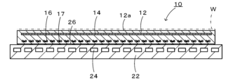
次に、本発明の実施の形態を図面に基づいて説明する。図1は本実施形態の静電チャックヒータ10の斜視図、図2は図1のA-A断面図、図3は抵抗発熱体16を平面視したときの説明図、図4は図3のB-B断面図である。
Next, embodiments of the present invention will be described based on the drawings. 1 is a perspective view of the
静電チャックヒータ10は、セラミック基板12の内部に静電電極14と抵抗発熱体16とが埋設されたものである。静電チャックヒータ10の裏面には、冷却板22が接着層26を介して接着されている。
The
セラミック基板12は、セラミックス製(例えばアルミナ製や窒化アルミニウム製)の円板である。セラミック基板12の表面には、ウエハWを載置可能なウエハ載置面12aが設けられている。
The
静電電極14は、ウエハ載置面12aに略平行な円形の導電性薄膜である。この静電電極14には、図示しない棒状端子が電気的に接続されている。棒状端子は、静電電極14の下面からセラミック基板12を経たあと冷却板22を通って下方に延び出している。棒状端子は、冷却板22と電気的に絶縁されている。セラミック基板12のうち静電電極14より上側の部分は、誘電体層として機能する。静電電極14の材料としては、例えば炭化タングステン、金属タングステン、炭化モリブデン、金属モリブデンなどが挙げられ、このうち、使用するセラミックと熱膨張係数の近いものを選ぶことが好ましい。
The
抵抗発熱体16は、ウエハ載置面12aに略平行な面に設けられた帯状の導電性ラインである。帯状の導電性ラインは、特に限定するものではないが、例えば幅0.1~10mm、厚み0.001~0.1mm、線間距離0.1~5mmに設定されていてもよい。抵抗発熱体16は、一方の端子部18から他方の端子部20まで一筆書きの要領でセラミック基板12の全体にわたって帯状の導電性ラインを交差しないように配線したものである。抵抗発熱体16の端子部18,20のそれぞれには、図示しない給電端子が個別に電気的に接続されている。これらの給電端子は、抵抗発熱体16の下面からセラミック基板12を通過したあと冷却板22を通って下方に延び出している。また、これらの給電端子は、冷却板22と電気的に絶縁されている。抵抗発熱体16の材料としては、例えば炭化タングステン、金属タングステン、炭化モリブデン、金属モリブデンなどが挙げられ、このうち、使用するセラミックと熱膨張係数の近いものを選ぶことが好ましい。
The
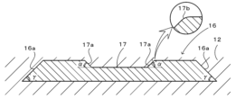
抵抗発熱体16の表面には、図4に示すように、抵抗発熱体16の長手方向(電流の流れる方向)に沿って凹溝17が設けられている。凹溝17の深さは、当然のことながら抵抗発熱体16の厚みよりも小さいが、抵抗発熱体16の厚みの半分以下であることが好ましい。凹溝17の側壁面17aは、セラミック基板12のウエハ載置面12aに対して傾斜している。凹溝17の側壁面17aとセラミック基板12との間には空隙が存在しない。なお、「空隙が存在しない」とは、倍率150倍のセラミック基板12のSEM断面を肉眼で見たときに空隙が確認されないことをいう(以下同じ)。ウエハ載置面12aに対する側壁面17aの傾斜角度αは27°以下であることが好ましい。また、この傾斜角度αは加工性を考慮すると10°以上であることが好ましい。凹溝17の幅は、凹溝17の深さ以上であることが好ましい。凹溝17の開口縁17bは、角張っておらず面取りされた形状である。面取りは、C面取りでもよいしR面取りでもよい。セラミック基板12のウエハ載置面12aに対して抵抗発熱体16の長手方向に沿う端面16aは、傾斜している。端面16aとセラミック基板12との間には空隙が存在しない。ウエハ載置面12aに対する端面16aの傾斜角度γは27°以下であることが好ましい。抵抗発熱体16の端面16aの傾斜角度γは、凹溝17の側壁面17aの傾斜角度αよりも小さいことが好ましい。
As shown in FIG. 4,
冷却板22は、金属製(例えばアルミニウム製)であり、冷媒(例えば水)が通過可能な冷媒通路24を内蔵している。この冷媒通路24は、セラミック基板12の全面にわたって冷媒が通過するように形成されている。なお、冷媒通路24には、冷媒の供給口と排出口(いずれも図示せず)が設けられている。
The cooling
次に、静電チャックヒータ10の使用例について説明する。この静電チャックヒータ10のウエハ載置面12aにウエハWを載置し、静電電極14とウエハWとの間に電圧を印加することによりウエハWを静電気的な力によってウエハ載置面12aに吸着する。この状態で、ウエハWにプラズマCVD成膜を施したりプラズマエッチングを施したりする。また、抵抗発熱体16に電圧を印加してウエハWを加熱したり、冷却板22の冷媒通路24に冷媒を循環してウエハWを冷却したりすることにより、ウエハWの温度を一定に制御する。抵抗発熱体16に電圧を印加する際には、抵抗発熱体16の一方の端子部18と他方の端子部20との間に電圧を印加する。すると、抵抗発熱体16に電流が流れ、それによって抵抗発熱体16が発熱してウエハWを加熱する。
Next, an example of use of the
本実施形態では、抵抗発熱体16の表面には凹溝17が形成されている。抵抗発熱体16は、一方の端子部18から他方の端子部20までを複数の区間に分割され、区間ごとに凹溝17(深さは略一定)の幅が決定されている。凹溝17の幅の広い区間は、抵抗発熱体16の断面積が小さくなるため抵抗が高くなり発熱量が大きくなる。凹溝17の幅の狭い区間は、抵抗発熱体16の断面積が大きくなるため抵抗が低くなり発熱量が小さくなる。そのため、各区間の凹溝17の幅を調整することにより、抵抗発熱体16の区間ごとの発熱量を目標発熱量に一致させている。
In this embodiment,
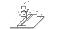
次に、静電チャックヒータ10の製造例について説明する。図5は静電チャックヒータ10の製造工程図、図6は抵抗発熱体前駆体66の幅方向を含む面で抵抗発熱体前駆体66を垂直に切断したときの抵抗発熱体前駆体66の断面図、図7は抵抗発熱体前駆体66に凹溝67を形成する工程の説明図、図8及び図9は抵抗発熱体前駆体66の幅方向を含む面で抵抗発熱体前駆体66を垂直に切断したときの線溝68及び凹溝67の断面図である。以下には、セラミック基板12としてアルミナ基板を製造する場合を例に挙げて説明する。
Next, a manufacturing example of the
[1]成形体の作製(図5(A)参照)
円盤状の下部及び上部の成形体51,53を作製する。各成形体51,53は、例えば、まず、成形型にアルミナ粉体(例えば平均粒径0.1~10μm)、溶媒、分散剤及びゲル化剤を含むスラリーを投入し、成形型内でゲル化剤を化学反応させてスラリーをゲル化させたあと離型することにより、作製する。このようにして得られる成形体51,53を、モールドキャスト成形体と称する。[1] Preparation of molded body (see Figure 5(A))
Disc-shaped lower and upper molded
溶媒としては、分散剤及びゲル化剤を溶解するものであれば、特に限定されないが、例えば、炭化水素系溶媒(トルエン、キシレン、ソルベントナフサ等)、エーテル系溶媒(エチレングリコールモノエチルエーテル、ブチルカルビトール、ブチルカルビトールアセテート等)、アルコール系溶媒(イソプロパノール、1-ブタノール、エタノール、2-エチルヘキサノール、テルピネオール、エチレングリコール、グリセリン等)、ケトン系溶媒(アセトン、メチルエチルケトン等)、エステル系溶媒(酢酸ブチル、グルタル酸ジメチル、トリアセチン等)、多塩基酸系溶媒(グルタル酸等)が挙げられる。特に、多塩基酸エステル(例えば、グルタル酸ジメチル等)、多価アルコールの酸エステル(例えば、トリアセチン等)等の、2以上のエステル結合を有する溶媒を使用することが好ましい。 The solvent is not particularly limited as long as it dissolves the dispersant and gelling agent, but examples include hydrocarbon solvents (toluene, xylene, solvent naphtha, etc.), ether solvents (ethylene glycol monoethyl ether, butyl Carbitol, butyl carbitol acetate, etc.), alcohol solvents (isopropanol, 1-butanol, ethanol, 2-ethylhexanol, terpineol, ethylene glycol, glycerin, etc.), ketone solvents (acetone, methyl ethyl ketone, etc.), ester solvents ( butyl acetate, dimethyl glutarate, triacetin, etc.), and polybasic acid solvents (glutaric acid, etc.). In particular, it is preferable to use a solvent having two or more ester bonds, such as a polybasic acid ester (for example, dimethyl glutarate, etc.) or an acid ester of a polyhydric alcohol (for example, triacetin, etc.).
分散剤としては、アルミナ粉体を溶媒中に均一に分散するものであれば、特に限定されない。例えば、ポリカルボン酸系共重合体、ポリカルボン酸塩、ソルビタン脂肪酸エステル、ポリグリセリン脂肪酸エステル、リン酸エステル塩系共重合体、スルホン酸塩系共重合体、3級アミンを有するポリウレタンポリエステル系共重合体等が挙げられる。特に、ポリカルボン酸系共重合体、ポリカルボン酸塩等を使用することが好ましい。この分散剤を添加することで、成形前のスラリーを、低粘度とし、且つ高い流動性を有するものとすることができる。 The dispersant is not particularly limited as long as it can uniformly disperse the alumina powder in the solvent. For example, polycarboxylic acid copolymers, polycarboxylate salts, sorbitan fatty acid esters, polyglycerin fatty acid esters, phosphate ester salt copolymers, sulfonate salt copolymers, polyurethane polyester copolymers containing tertiary amines, etc. Examples include polymers. In particular, it is preferable to use polycarboxylic acid copolymers, polycarboxylic acid salts, and the like. By adding this dispersant, the slurry before molding can be made to have low viscosity and high fluidity.
ゲル化剤としては、例えば、イソシアネート類、ポリオール類及び触媒を含むものとしてもよい。このうち、イソシアネート類としては、イソシアネート基を官能基として有する物質であれば特に限定されないが、例えば、トリレンジイソシアネート(TDI)、ジフェニルメタンジイソシアネート(MDI)又はこれらの変性体等が挙げられる。なお、分子内おいて、イソシアネート基以外の反応性官能基が含有されていてもよく、更には、ポリイソシアネートのように、反応性官能基が多数含有されていてもよい。ポリオール類としては、イソシアネート基と反応し得る水酸基を2以上有する物質であれば特に限定されないが、例えば、エチレングリコール(EG)、ポリエチレングリコール(PEG)、プロピレングリコール(PG)、ポリプロピレングリコール(PPG)、ポリテトラメチレングリコール(PTMG)、ポリヘキサメチレングリコール(PHMG)、ポリビニルアルコール(PVA)等が挙げられる。触媒としては、イソシアネート類とポリオール類とのウレタン反応を促進させる物質であれば特に限定されないが、例えば、トリエチレンジアミン、ヘキサンジアミン、6-ジメチルアミノ-1-ヘキサノール等が挙げられる。 The gelling agent may include, for example, isocyanates, polyols, and catalysts. Among these, isocyanates are not particularly limited as long as they have an isocyanate group as a functional group, and examples include tolylene diisocyanate (TDI), diphenylmethane diisocyanate (MDI), and modified products thereof. Note that the molecule may contain reactive functional groups other than isocyanate groups, and may further contain a large number of reactive functional groups like polyisocyanate. Polyols are not particularly limited as long as they have two or more hydroxyl groups that can react with isocyanate groups, but examples include ethylene glycol (EG), polyethylene glycol (PEG), propylene glycol (PG), and polypropylene glycol (PPG). , polytetramethylene glycol (PTMG), polyhexamethylene glycol (PHMG), polyvinyl alcohol (PVA), and the like. The catalyst is not particularly limited as long as it is a substance that promotes the urethane reaction between isocyanates and polyols, and examples thereof include triethylenediamine, hexanediamine, 6-dimethylamino-1-hexanol, and the like.
この工程では、まず、アルミナ粉体に溶媒及び分散剤を所定の割合で添加し、所定時間に亘ってこれらを混合することによりスラリー前駆体を調製し、その後、このスラリー前駆体に、ゲル化剤を添加して混合・真空脱泡してスラリーとするのが好ましい。スラリー前駆体やスラリーを調製するときの混合方法は、特に限定されるものではなく、例えばボールミル、自公転式撹拌、振動式撹拌、プロペラ式撹拌等を使用可能である。なお、スラリー前駆体にゲル化剤を添加したスラリーは、時間経過に伴いゲル化剤の化学反応(ウレタン反応)が進行し始めるため、速やかに成形型内に流し込むのが好ましい。成形型に流し込まれたスラリーは、スラリーに含まれるゲル化剤が化学反応することによりゲル化する。ゲル化剤の化学反応とは、イソシアネート類とポリオール類とがウレタン反応を起こしてウレタン樹脂(ポリウレタン)になる反応である。ゲル化剤の反応によりスラリーがゲル化し、ウレタン樹脂は有機バインダとして機能する。 In this process, a slurry precursor is first prepared by adding a solvent and a dispersant to alumina powder in a predetermined ratio and mixing them for a predetermined time. It is preferable to add an agent, mix and vacuum defoaming to form a slurry. The mixing method when preparing the slurry precursor or slurry is not particularly limited, and for example, a ball mill, rotational stirring, vibrational stirring, propeller stirring, etc. can be used. Note that it is preferable to quickly pour the slurry, which is a slurry precursor containing a gelling agent, into a mold because the chemical reaction (urethane reaction) of the gelling agent begins to proceed over time. The slurry poured into the mold is gelled by a chemical reaction of the gelling agent contained in the slurry. The chemical reaction of the gelling agent is a reaction in which isocyanates and polyols undergo a urethane reaction to form a urethane resin (polyurethane). The slurry gels due to the reaction of the gelling agent, and the urethane resin functions as an organic binder.
[2]仮焼体の作製(図5(B)参照)
下部及び上部の成形体51,53を乾燥したあと脱脂し、更に仮焼することにより、下部及び上部の仮焼体61,63を得る。成形体51,53の乾燥は、成形体51,53に含まれる溶媒を蒸発させるために行う。乾燥温度や乾燥時間は、使用する溶媒に応じて適宜設定すればよい。但し、乾燥温度は、乾燥中の成形体51,53にクラックが入らないように注意して設定する。また、雰囲気は大気雰囲気、不活性雰囲気、真空雰囲気のいずれであってもよい。乾燥後の成形体51,53の脱脂は、分散剤や触媒やバインダなどの有機物を分解・除去するために行う。脱脂温度は、含まれる有機物の種類に応じて適宜設定すればよいが、例えば400~600℃に設定してもよい。また、雰囲気は大気雰囲気、不活性雰囲気、真空雰囲気のいずれであってもよい。脱脂後の成形体51,53の仮焼は、強度を高くしハンドリングしやすくするために行う。仮焼温度は、特に限定するものではないが、例えば750~900℃に設定してもよい。また、雰囲気は大気雰囲気、不活性雰囲気、真空雰囲気のいずれであってもよい。[2] Preparation of calcined body (see Figure 5(B))
The lower and upper molded
[3]抵抗発熱体前駆体の形成(図5(C)及び図6参照)
下部の仮焼体61の片面に抵抗発熱体用ペーストを抵抗発熱体16と同じパターンとなるように印刷したあと乾燥することにより抵抗発熱体前駆体66を形成する。また、上部の仮焼体63の片面に静電電極用ペーストを静電電極14と同じ形状となるように印刷したあと乾燥することにより静電電極前駆体64を形成する。両ペーストは、いずれも、アルミナ粉体と導電性粉末とバインダと溶媒とを含むものである。アルミナ粉体としては、例えば成形体51,53の作製時に用いたものと同様のものを用いることができる。導電性粉末としては、例えば、炭化タングステン粉末が挙げられる。バインダとしては、例えば、セルロース系バインダ(エチルセルロースなど)やアクリル系バインダ(ポリメタクリル酸メチルなど)やビニル系バインダ(ポリビニルブチラールなど)が挙げられる。溶媒としては、例えば、テルピネオールなどが挙げられる。印刷方法は、例えば、スクリーン印刷法などが挙げられる。印刷は複数回実施する。そのため、各前駆体66,64は、多層構造となっている。また、抵抗発熱体前駆体66は、長手方向に沿う端面66aが階段状になるように印刷する(図6参照)。印刷されたペーストの端部は垂れるため最終的には端面66aは階段状ではなく傾斜面になる。端面66aは、下部の仮焼体61の表面に対して傾斜しており、その傾斜角度δは45°以下であることが好ましい。静電電極前駆体64も、図示しないがこれと同様に階段状になるように印刷する。この場合も、印刷されたペーストの端部は垂れるため最終的には端面は階段状ではなく傾斜面になる。[3] Formation of resistance heating element precursor (see FIG. 5(C) and FIG. 6)
A resistive
[4]凹溝の形成(図5(D)及び図7~9参照)
下部の仮焼体61の片面に設けた抵抗発熱体前駆体66に凹溝67を形成する。凹溝67の深さは、抵抗発熱体前駆体66の半分以下であることが好ましい。凹溝67の形成は、図7に示すピコ秒レーザ加工機30により行う。ピコ秒レーザ加工機30は、ガルバノミラーのモータとステージのモータを駆動させながらレーザ光32を抵抗発熱体前駆体66の長手方向に沿って照射することにより線溝68を形成する。線溝68の幅(1回のパスで形成される溝幅)は特に限定するものではないが、例えば10~100μmが好ましく、20~60μmがより好ましい。ピコ秒レーザ加工機30は、こうした線溝68を抵抗発熱体前駆体66の幅方向に重なるように複数本設けることにより、凹溝67を形成する。レーザ光32は、照射位置の中心で最もエネルギーが高く、中心よりも外側に行くほどエネルギーが低くなる。そのため、生成する線溝68の断面は、図8に示すようにサインカーブに近い形状になる。線溝68のピッチを線溝68の幅の半分になるように設定すると、現在の線溝68から次の線溝68を形成する際のレーザ光32の断面は図8の点線、その次の線溝68を形成する際のレーザ光32の断面は図8の1点鎖線、更にその次の線溝68を形成する際のレーザ光32の断面は図8の2点鎖線のようになる。そのため、これらすべての線溝68を形成し終えると、図9に示すように底面がほぼ平らに近い凹溝67が得られる。凹溝67は、線溝68の集合体である。凹溝67の側壁面67aは、下部の仮焼体61の表面に対して傾斜している。下部の仮焼体61の表面に対する凹溝67の側壁面67aの傾斜角度β(図9参照)は、45°以下であることが好ましい。また、レーザ光32の加工性を考慮すると、傾斜角度βは、18°以上であることが好ましい。傾斜角度βは、レーザ光32の出力やレーザ光32の加工回数(同じ箇所に照射するレーザ光32の回数)によって変化する。このとき、傾斜角度βの方が傾斜角度δよりも大きくなるようにする、換言すれば、傾斜角度δの方が傾斜角度βよりもなだらかになるようにすることが好ましい。[4] Formation of grooves (see Figure 5(D) and Figures 7 to 9)
A
凹溝67を形成するにあたっては、まず、凹溝67を形成する前の抵抗発熱体前駆体66の厚み分布をレーザ変位計を用いて測定する。この測定は、抵抗発熱体前駆体66の中心線に沿って予め定められた複数の測定点において実施する。各測定点において予め定められた厚みの目標値と厚みの測定値との差(厚みの差)を求める。厚みの目標値は、抵抗発熱体前駆体66を焼成して抵抗発熱体16としたときの抵抗の目標値に基づいて設定される。そして、ある測定点の厚みの差に基づいて、その測定点からその隣の測定点までの区間に形成する線溝68の本数を決定する。線溝68の深さは予め定められた値である。そのため、線溝68の本数を変化させることにより、凹溝67の幅が変化し、凹溝67の断面積ひいては抵抗発熱体前駆体66の断面積が変化する。つまり、凹溝67は、複数の測定点における抵抗発熱体前駆体66の断面積がそれぞれ予め定められた目標断面積になるように形成される。
In forming the
[5]積層体の作製(図5(E)参照)
下部の仮焼体61の抵抗発熱体前駆体66が設けられた面に、抵抗発熱体前駆体66を覆うようにアルミナ粉体を積層し、その上に上部の仮焼体63を、静電電極前駆体64が設けられた面がアルミナ粉体に接するように積層して成形し、積層体50を得る。積層体50は、上部及び下部の仮焼体61,63の間にアルミナ粉体層62が挟まれた構造である。アルミナ粉体としては、成形体51,53の作製時に用いたものと同様のものを用いることができる。[5] Fabrication of laminate (see Figure 5(E))
Alumina powder is layered on the surface of the lower
[6]ホットプレス焼成(図5(F)参照)
得られた積層体50を厚み方向に圧力を加えながらホットプレス焼成する。このとき、積層体50は、金型によって径方向に拡がらないようにせき止められているため厚さ方向に圧縮される。圧縮率は、プレス圧力によって異なるが、例えば30~70%である。これにより、抵抗発熱体前駆体66が焼成されて抵抗発熱体16となり、静電電極前駆体64が焼成されて静電電極14となり、仮焼体61、63及びアルミナ粉体層62が焼結して一体化してセラミック基板12となる。その結果、静電チャックヒータ10が得られる。ホットプレス焼成では、少なくとも最高温度(焼成温度)において、プレス圧力を30~300kgf/cm2とすることが好ましく、50~250kgf/cm2とすることがより好ましい。また、最高温度は、セラミック粉末の種類、粒径などにより適宜設定すればよいが、1000~2000℃の範囲に設定することが好ましい。雰囲気は、大気雰囲気、不活性雰囲気、真空雰囲気の中から、適宜選択すればよい。[6] Hot press firing (see Figure 5 (F))
The obtained
ここで、本実施形態の構成要素と本発明の構成要素との対応関係を明らかにする。本実施形態の静電チャックヒータ10が本発明のセラミックヒータに相当する。また、本実施形態の抵抗発熱体前駆体の形成(図5(C)及び図6参照)が本発明の工程(a)に相当し、凹溝の形成(図5(D)及び図7~9参照)が工程(b)に相当し、積層体の作製(図5(E)参照)が工程(c)に相当し、ホットプレス焼成(図5(F)参照)が工程(d)に相当し、仮焼体61が第1セラミック焼成層に相当し、アルミナ粉体層62が第2セラミック未焼成層に相当する。
Here, the correspondence between the constituent elements of this embodiment and the constituent elements of the present invention will be clarified. The
以上詳述した本実施形態では、抵抗発熱体前駆体66に凹溝67を形成することにより抵抗発熱体前駆体66の断面積(ひいては抵抗発熱体16の抵抗)を調整する。このとき、下部の仮焼体61の表面に対して凹溝67の側壁面67aが傾斜するように凹溝67を形成する。積層体50をホットプレス焼成する際、凹溝67の側壁面67aが傾斜しているため、凹溝67の側壁面67aとアルミナ粉体層62に含まれるアルミナ粉体との間に圧力が加わり、両者が緊密に接触した状態で積層体50が焼成される。これにより、静電チャックヒータ10において、凹溝17の側壁面17aとセラミック基板12との間に空隙が発生するのを防止すると共に、凹溝17の側壁面17aとセラミック基板12との接着強度を上げることができる。したがって、得られた静電チャックヒータ10の熱伝導性や均熱性が良好になる。
In the present embodiment described in detail above, the cross-sectional area of the resistance heating element precursor 66 (and thus the resistance of the resistance heating element 16) is adjusted by forming the
また、仮焼体61の表面に対する凹溝67の側壁面67aの傾斜角度βが45°以下であれば、静電チャックヒータ10の抵抗発熱体16の凹溝17の側壁面17aとセラミック基板12との間に空隙が発生するのを確実に防止することができる。傾斜角度βは、加工性(例えばレーザ光による加工回数など)を考慮すると18°以上であることが好ましい。傾斜角度βが小さすぎると、1回のレーザ光による加工で形成される凹溝17の深さが浅くなるため、凹溝17を所定の深さにするには加工回数が増えてしまい、加工時間が長くかかるからである。
Further, if the inclination angle β of the
更に、抵抗発熱体前駆体66の長手方向に沿って定められた複数の測定点における断面積がそれぞれ予め定められた目標断面積になるように凹溝67が形成される。そのため、抵抗発熱体前駆体66の抵抗を測定することなく凹溝67の形状を決定することができる。
Furthermore, the
凹溝67の深さは、抵抗発熱体前駆体66の厚みの半分以下にするのが好ましい。こうすれば、凹溝67の深さが深すぎる場合に比べて、静電チャックヒータ10の凹溝17の側壁面17aとセラミック基板12との間に空隙が発生するのをより防止しやすくなる。
The depth of the
更にまた、仮焼体61の表面に対して抵抗発熱体前駆体66の長手方向に沿う端面66aが傾斜している。そのため、静電チャックヒータ10の抵抗発熱体16の長手方向に沿った端面16aとセラミック基板12との間に空隙が発生するのを防止すると共に、その端面16aとセラミック基板12との接着強度を上げることができる。したがって、得られた静電チャックヒータ10の熱伝導性や均熱性がより良好になる。特に、仮焼体61の表面に対する抵抗発熱体前駆体66の長手方向に沿う端面の傾斜角度δが45°以下であれば、抵抗発熱体16の長手方向に沿う端面16aとセラミック基板12との間に空隙が発生するのを確実に防止することができる。
Furthermore, the end face 66a of the resistance
凹溝67を形成するにあたり、凹溝67の側壁67aの傾斜角度βの方が抵抗発熱体前駆体66の端面66aの傾斜角度δよりも大きくなるようにする、換言すれば傾斜角度δの方が傾斜角度βよりもなだらかになるようにするのが好ましい。抵抗発熱体前駆体66の高さは、凹溝67の深さよりも大きい。そのため、抵抗発熱体前駆体66の端面66aの傾斜の方がよりなだらかになるようにすることによって、静電チャックヒータ10の抵抗発熱体16の端面16aとセラミック基板12との間に空隙が発生するのをより防止することができる。
When forming the
そして、静電チャックヒータ10は、凹溝17の側壁面17aはセラミック基板12の表面に対して傾斜しており、凹溝17の側壁面17aとセラミック基板12との間には空隙が存在しない。そのため、静電チャックヒータ10の熱伝導性や均熱性が良好になる。セラミック基板12の表面に対する凹溝17の側壁面17aの傾斜角度αは27°以下が好ましい。また、傾斜角度αは10°以上が好ましい。凹溝17の側壁面17aとセラミック基板12との間に空隙が発生するのをより確実に防止するには、凹溝17の幅を凹溝17の深さ以上に設定することが好ましい。
In the
そしてまた、静電チャックヒータ10は、凹溝17の開口縁17bは面取りされた形状となっている。そのため、凹溝17の開口縁が角張っている場合に比べて、凹溝17の開口縁17bを起点とするクラックが発生しにくくなる。なお、ホットプレス焼成を行う前の凹溝67の開口縁が角張っていたとしても、ホットプレス焼成後の凹溝17の開口縁17bは面取りされた形状になる。凹溝17の深さは、抵抗発熱体16の厚みの半分以下であることが好ましい。
Further, in the
そして更に、静電チャックヒータ10は、セラミック基板12の表面に対して抵抗発熱体16の長手方向に沿う端面16aが傾斜しており、端面16aとセラミック基板12との間には空隙が存在しない。そのため、静電チャックヒータ10の熱伝導性や均熱性がより良好になる。セラミック基板12の表面に対する抵抗発熱体16の長手方向に沿う端面16aの傾斜角度γは27°以下であることが好ましい。傾斜角度γは、凹溝17の側壁面17aの傾斜角度αよりも小さいことが好ましい。
Further, in the
なお、本発明は上述した実施形態に何ら限定されることはなく、本発明の技術的範囲に属する限り種々の態様で実施し得ることはいうまでもない。 It goes without saying that the present invention is not limited to the embodiments described above, and can be implemented in various forms as long as they fall within the technical scope of the present invention.
例えば、上述した実施形態では、セラミックヒータとして静電チャックヒータ10を例示したが、静電電極14を有さないセラミックヒータであってもよい。この場合、静電電極前駆体64を有さない上部の仮焼体63を用いて積層体50を作製しその積層体50をホットプレス焼成してもよいし、上部の仮焼体63を省略して積層体50を作製しその積層体50をホットプレス焼成してもよい。
For example, in the embodiment described above, the
上述した実施形態では、第2セラミック未焼成層としてアルミナ粉体層62を例示したが、アルミナ粉体層62の代わりにアルミナ成形体層やアルミナグリーンシートを用いてもよい。アルミナ成形体層は、乾燥したものを用いてもよいし、乾燥後脱脂したものを用いてもよい。
In the embodiment described above, the
上述した実施形態では、第1セラミック焼成層として仮焼体61を例示したが、仮焼体61の代わりにアルミナ焼結体を用いてもよい。あるいは、第1セラミック焼成層の代わりにセラミック成形体層やセラミックグリーンシートを用いてもよい。セラミック成形体層は、乾燥したものを用いてもよいし、乾燥後脱脂したものを用いてもよい。
In the embodiment described above, the
上述した実施形態では、凹溝67を形成する抵抗発熱体前駆体66として、抵抗発熱体用ペーストを印刷したあと乾燥したものを用いたが、印刷し乾燥したあと脱脂したものや、印刷し乾燥し脱脂したあと仮焼(又は焼成)したものを用いてもよい。
In the embodiment described above, the resistive
上述した実施形態では、抵抗発熱体16としてセラミック基板12の全体に一筆書きの要領で帯状の導電性ラインを交差しないように配線したものを採用したが、特にこれに限定されるものではない。例えば、セラミック基板12を複数のゾーンに分け、ゾーンごとに一筆書きの要領で帯状の導電性ラインを交差しないように配線した抵抗発熱体を設けてもよい。この場合、各抵抗発熱体は、上述した抵抗発熱体16と同様の構造を採用すればよい。
In the embodiment described above, the
以下に、本発明の実施例について説明する。なお、以下の実施例は本発明を何ら限定するものではない。 Examples of the present invention will be described below. Note that the following examples do not limit the present invention in any way.
[実施例1]
上述した製造例にしたがって静電チャックヒータ10を作製した(図5参照)。
[1]成形体の作製
アルミナ粉末(平均粒径0.5μm,純度99.7%)100重量部、マグネシア0.04重量部、分散剤としてポリカルボン酸系共重合体3重量部、溶媒として多塩基酸エステル20重量部を秤量し、これらをボールミル(トロンメル)で14時間混合し、スラリー前駆体とした。このスラリー前駆体に対して、ゲル化剤、すなわちイソシアネート類として4,4’・ジフェニルメタンジイソシアネート3.3重量部、ポリオール類としてエチレングリコール0.3重量部、触媒として6・ジメチルアミノ・1・ヘキサノール0.1重量部を加え、自公転式撹拌機で12分間混合し、スラリーを得た。得られたスラリーを、成形型に流し込んだ。その後、22℃で2時間放置することにより、成形型内でゲル化剤を化学反応させてスラリーをゲル化させたあと離型した。これにより、上部及び下部の成形体51,53(図5(A)参照)を得た。[Example 1]
An
[1] Preparation of molded body 100 parts by weight of alumina powder (average particle size 0.5 μm, purity 99.7%), 0.04 parts by weight of magnesia, 3 parts by weight of polycarboxylic acid copolymer as a dispersant, as a solvent 20 parts by weight of the polybasic acid ester were weighed and mixed in a ball mill (trommel) for 14 hours to obtain a slurry precursor. To this slurry precursor, a gelling agent, that is, 3.3 parts by weight of 4,4'-diphenylmethane diisocyanate as an isocyanate, 0.3 part by weight of ethylene glycol as a polyol, and 6-dimethylamino-1-hexanol as a catalyst. 0.1 part by weight was added and mixed for 12 minutes using a rotation-revolution type stirrer to obtain a slurry. The obtained slurry was poured into a mold. Thereafter, the slurry was left to stand at 22° C. for 2 hours to chemically react the gelling agent in the mold to gel the slurry, and then the mold was released. As a result, upper and lower molded
[2]仮焼体の作製
上部及び下部の成形体51,53を100℃で10時間乾燥した後、最高温度500℃で1時間脱脂し、更に最高温度820℃、大気雰囲気で1時間仮焼することにより、上部及び下部の仮焼体61,63(図5(B)参照)を得た。[2] Preparation of calcined bodies After drying the upper and lower molded
[3]抵抗発熱体前駆体の形成
炭化タングステン粉末(平均粒径1.5μm)とアルミナ粉末(平均粒径0.5μm)をアルミナ含有量が10重量%となるように混合し、バインダーとしてポリメタクリル酸メチルと溶媒としてテルピネオールを加えて混合することによりペーストを調製した。このペーストは、抵抗発熱体用、静電電極用の両方に用いることとした。そして、下部の仮焼体61の片面に抵抗発熱体用ペーストを複数回スクリーン印刷し、その後乾燥することで厚さ100μmの抵抗発熱体前駆体66を形成した。また、上部の仮焼体63の片面に静電電極用ペーストを複数回スクリーン印刷し、その後乾燥することで静電電極前駆体64を形成した(図5(C)参照)。抵抗発熱体前駆体66の端面66aの傾斜角度δは10°であった。実際には印刷されたペーストの端部は垂れるため、端面66aは階段状ではなく傾斜面になった。静電電極前駆体64の端面の傾斜角度も同じ値であった。[3] Formation of resistance heating element precursor Tungsten carbide powder (average particle size 1.5 μm) and alumina powder (average particle size 0.5 μm) were mixed so that the alumina content was 10% by weight, and polyester was used as a binder. A paste was prepared by adding and mixing methyl methacrylate and terpineol as a solvent. This paste was used for both resistive heating elements and electrostatic electrodes. Then, a resistive heating element paste was screen printed multiple times on one side of the lower
[4]凹溝の形成
抵抗発熱体前駆体66の厚み分布をレーザ変位計を用いて測定し、測定結果に基づいてピコ秒レーザ加工機30を用いて抵抗発熱体前駆体66の表面に凹溝67を形成した。レーザ加工条件は、レーザ出力20W、加工速度2000mm/sec、加工回数2回とした。形成された凹溝67の形状測定を行った。その結果を図10に示す。図10から、凹溝67の深さは20μm、凹溝67の側壁面67aの傾斜角度βは34°であった。[4] Formation of grooves The thickness distribution of the resistance
ここで、傾斜角度βの求め方を説明する。まず、図11に示すように、傾斜面である側壁面67aを含むように幅方向に0.5mmの対象範囲を設定した。このとき、抵抗発熱体前駆体66の底面がほぼ水平になるように補正すると共に、対象範囲の中心と側壁面67aの真ん中とを概ね一致させた。この対象範囲の全域にわたって、幅方向に2.5μmピッチで抵抗発熱体前駆体66の高さを取得した。高さは、触針式測定器を用いて測定した。そして、横軸に抵抗発熱体前駆体66の高さ、縦軸に度数をとったグラフ(ヒストグラム)を作成した。高さのデータ間隔は1μmとした。ヒストグラムの一例を図12に示す。ヒストグラムには、高さの低い第1グループと高さの高い第2グループとが現れた。第1グループは、凹溝67の底面の高さのグループであり、第2グループは、抵抗発熱体前駆体66の頂面(凹溝67が設けられていない部分)の高さのグループである。ヒストグラムにおいて、第1グループ内で最も度数の高い値(最頻値)を凹溝67の底面高さHLとみなし、第2グループ内で最も度数の高い値(最頻値)を抵抗発熱体前駆体66の頂面高さHUとみなした。また、HUからHLを減算した値を凹溝67の深さDとした。そして、HLに0.1Dを加算した値を下限値、HUから0.1Dを減算した値を上限値とし、側壁面67aのうち下限値から上限値までの間で2.5μmピッチで測定した高さを用いて側壁面67aの回帰直線を求め、その回帰直線が水平線(図10の横軸)となす角度を傾斜角度βとした。なお、前出の抵抗発熱体前駆体66の端面66aの傾斜角度δもこれと同様にして求めた。但し、傾斜角度δを求める際には対象範囲を0.5mmではなく1.5mmに設定した。
Here, a method for determining the inclination angle β will be explained. First, as shown in FIG. 11, a target range of 0.5 mm in the width direction was set to include the
[5]積層体の作製
仮焼体61の抵抗発熱体前駆体66が設けられた面に、抵抗発熱体前駆体66を覆うようにアルミナ粉体を積層し、その上に仮焼体63を、静電電極前駆体64が設けられた面がアルミナ粉体に接するように積層して成形し、積層体50を得た。[5] Preparation of laminate Alumina powder is laminated on the surface of the
[6]ホットプレス焼成
得られた積層体50のホットプレス焼成を行った。これにより、抵抗発熱体前駆体66が焼成されて厚さ50μmの抵抗発熱体16となり、静電電極前駆体64が焼成されて静電電極14となり、仮焼体61、63及びアルミナ粉体層62が焼結して一体化してセラミック基板12となり、静電チャックヒータ10を得た。ホットプレス焼成は、真空雰囲気下、圧力250kgf/cm2、最高温度1600℃で2時間保持することにより行った。その後、セラミック焼結体表面をダイヤモンド砥石にて平面研削加工を行い、静電電極14からウエハ載置面12aまでの厚みを350μmとした。[6] Hot Press Firing The obtained
[評価]
得られた静電チャックヒータ10のセラミック基板(アルミナ基板)12の外観を観察したところ、色調に差がある箇所は見られなかった。また、得られた静電チャックヒータ10の断面のSEM写真(倍率150倍、画素数16.5万画素以上)から、凹溝17の深さは10μm、凹溝17の側壁面17aの傾斜角度αは18°であった。凹溝17の深さ及び傾斜角度αは、SEM写真を用いて前出の凹溝67の深さD及び傾斜角度βの求め方と同様にして求めた。また、SEM写真において、凹溝17の側壁面17aとセラミック基板(アルミナ基板)12との間には空隙は見られなかった。抵抗発熱体16の長手方向に沿った端面16aの傾斜角度γは5°であった。傾斜角度γは、SEM写真を用いて前出の傾斜角度δの求め方と同様にして求めた。静電電極14の端面の傾斜角度も同じく5°であった。各端面とセラミック基板12との間にも空隙は見られなかった。[evaluation]
When the appearance of the ceramic substrate (alumina substrate) 12 of the obtained
[実施例2]
上述した実施例1のレーザ加工条件の加工回数を1回とした以外は、実施例1と同様にして静電チャックヒータ10を作製した。抵抗発熱体前駆体66の凹溝67の深さは10μm、傾斜角度βは18°、抵抗発熱体前駆体66の端面66aの傾斜角度δや静電電極前駆体64の端面の傾斜角度は10°であった。実施例1と同様にして静電チャックヒータ10の断面のSEM写真を撮影し観察したところ、凹溝17の深さは5μm、凹溝17の側壁面17aの傾斜角度αは10°であった。凹溝67の側壁面67aとセラミック基板12との間には空隙は見られなかった。抵抗発熱体16の長手方向に沿った端面の傾斜角度γは5°であった。静電電極14の端面の傾斜角度も同じく5°であった。各端面とセラミック基板12との間にも空隙は見られなかった。なお、各傾斜角度は実施例1と同様にして求めた。[Example 2]
The
[実施例3]
上述した実施例1のレーザ加工条件の加工回数を3回とした以外は、実施例1と同様にして静電チャックヒータ10を作製した。抵抗発熱体前駆体66の凹溝67の深さは30μm、傾斜角度βは45°、抵抗発熱体前駆体66の端面66aの傾斜角度δや静電電極前駆体64の端面の傾斜角度は10°であった。実施例1と同様にして静電チャックヒータ10の断面のSEM写真を撮影し観察したところ、凹溝17の深さは15μm、凹溝17の側壁面17aの傾斜角度αは27°であった。凹溝17の側壁面17aとセラミック基板12との間には空隙は見られなかった。抵抗発熱体16の長手方向に沿った端面の傾斜角度γは5°であった。静電電極14の端面の傾斜角度も同じく5°であった。各端面とセラミック基板12との間にも空隙は見られなかった。なお、各傾斜角度は実施例1と同様にして求めた。[Example 3]
The
実施例1~3の主な結果を表1に示す。 The main results of Examples 1 to 3 are shown in Table 1.

[実施例4及び5]
実施例4では、端面66aの傾斜角度δを18°とした以外は、上述した実施例1と同様にして静電チャックヒータ10を作製した。得られた抵抗発熱体16の長手方向に沿った端面16aの傾斜角度γは10°であった。実施例5では、端面66aの傾斜角度δを45°とした以外は、上述した実施例1と同様にして静電チャックヒータ10を作製した。得られた抵抗発熱体16の長手方向に沿った端面16aの傾斜角度γは26°であった。実施例4,5では抵抗発熱体16の端面16a付近に空隙(それに伴う均熱性異常)は確認されなかった。[Example 4 and 5]
In Example 4, the
本出願は、2020年2月26日に出願された日本国特許出願第2020-030724号を優先権主張の基礎としており、引用によりその内容の全てが本明細書に含まれる。 This application claims priority from Japanese Patent Application No. 2020-030724 filed on February 26, 2020, the entire contents of which are incorporated herein by reference.
本発明のセラミックヒータは、例えば半導体製造装置用部材として利用可能である。 The ceramic heater of the present invention can be used, for example, as a member for semiconductor manufacturing equipment.
10 静電チャックヒータ、12 セラミック基板、12a ウエハ載置面、14 静電電極、16 抵抗発熱体、16a 端面、17 凹溝、17a 側壁面、17b 開口縁、18,20 端子部、22 冷却板、24 冷媒通路、26 接着層、30 ピコ秒レーザ加工機、32 レーザ光、50 積層体、51,53 成形体、61,63 仮焼体、62 アルミナ粉体層、64 静電電極前駆体、66 抵抗発熱体前駆体、66a 端面、67 凹溝、67a 側壁面、68 線溝。 10 electrostatic chuck heater, 12 ceramic substrate, 12a wafer placement surface, 14 electrostatic electrode, 16 resistance heating element, 16a end surface, 17 groove, 17a side wall surface, 17b opening edge, 18, 20 terminal section, 22 cooling plate , 24 coolant passage, 26 adhesive layer, 30 picosecond laser processing machine, 32 laser beam, 50 laminate, 51, 53 molded body, 61, 63 calcined body, 62 alumina powder layer, 64 electrostatic electrode precursor, 66 resistance heating element precursor, 66a end face, 67 groove, 67a side wall surface, 68 line groove.
Claims (12)
(b)前記抵抗発熱体又はその前駆体にレーザ光を照射して前記抵抗発熱体又はその前駆体の長手方向に沿って凹溝を形成する工程と、
(c)前記第1セラミック焼成層又は未焼成層の表面に前記抵抗発熱体又はその前駆体を覆うように第2セラミック未焼成層を配置して積層体を得る工程と、
(d)前記積層体をホットプレス焼成することにより、セラミック基板の内部に前記抵抗発熱体が埋設されたセラミックヒータを得る工程と、
を含み、
前記工程(b)では、前記第1セラミック焼成層又は未焼成層の表面に対して前記凹溝の側壁面が傾斜し、前記第1セラミック焼成層又は未焼成層の表面に対する前記凹溝の側壁面の傾斜角度が45°以下になるように前記凹溝を形成する、
セラミックヒータの製法。 (a) forming a predetermined pattern of a resistance heating element or its precursor on the surface of the first ceramic fired layer or unfired layer;
(b) irradiating the resistive heating element or its precursor with a laser beam to form a groove along the longitudinal direction of the resistive heating element or its precursor;
(c) obtaining a laminate by disposing a second ceramic unfired layer on the surface of the first ceramic fired layer or unfired layer so as to cover the resistance heating element or its precursor;
(d) obtaining a ceramic heater in which the resistance heating element is embedded inside a ceramic substrate by hot-press firing the laminate;
including;
In the step (b), the side wall surface of the groove is inclined with respect to the surface of the first ceramic fired layer or unfired layer , and the side wall surface of the groove is inclined with respect to the surface of the first ceramic fired layer or unfired layer. forming the groove so that the inclination angle of the wall surface is 45° or less ;
Manufacturing method of ceramic heater.
請求項1に記載のセラミックヒータの製法。 In the step (b), the groove is formed so that the cross-sectional area at a plurality of measurement points determined along the longitudinal direction of the resistance heating element or its precursor becomes a predetermined target cross-sectional area. ,
A method for manufacturing a ceramic heater according to claim 1 .
請求項1又は2に記載のセラミックヒータの製法。 In the step (b), the depth of the groove is less than half the thickness of the resistance heating element or its precursor.
A method for manufacturing a ceramic heater according to claim 1 or 2 .
請求項1~3のいずれか1項に記載のセラミックヒータの製法。 In the step (a), the resistive heating element or its precursor is arranged such that the end face along the longitudinal direction of the resistive heating element or its precursor is inclined with respect to the surface of the first ceramic fired layer or the unfired layer. Form,
A method for manufacturing a ceramic heater according to any one of claims 1 to 3 .
請求項4に記載のセラミックヒータの製法。 In the step (a), the resistive heating element or its precursor is heated such that the inclination angle of the end face along the longitudinal direction of the resistive heating element or its precursor with respect to the surface of the first fired ceramic layer or the unfired layer is 45° or less. forming its precursor,
A method for manufacturing a ceramic heater according to claim 4 .
請求項4又は5に記載のセラミックヒータの製法。 In the step (b), the inclination angle of the side wall surface of the groove is larger than the inclination angle of the end face along the longitudinal direction of the resistance heating element or its precursor.
A method for manufacturing a ceramic heater according to claim 4 or 5 .
前記抵抗発熱体の表面に前記抵抗発熱体の長手方向に沿って設けられた凹溝と、
前記セラミック基板の表面に対して傾斜する前記凹溝の側壁面と、
を備え、
前記セラミック基板の表面に対する前記凹溝の側壁面の傾斜角度は27°以下であり、
前記凹溝の側壁面と前記セラミック基板との間には空隙が存在しない、
セラミックヒータ。 A ceramic heater in which a resistance heating element is embedded inside a ceramic substrate,
a groove provided on the surface of the resistance heating element along the longitudinal direction of the resistance heating element;
a side wall surface of the groove that is inclined with respect to the surface of the ceramic substrate;
Equipped with
The angle of inclination of the side wall surface of the groove with respect to the surface of the ceramic substrate is 27° or less,
There is no gap between the side wall surface of the groove and the ceramic substrate.
ceramic heater.
請求項7に記載のセラミックヒータ。 The opening edge of the groove has a chamfered shape.
The ceramic heater according to claim 7 .
請求項7又は8に記載のセラミックヒータ。 The depth of the groove is less than half the thickness of the resistance heating element,
The ceramic heater according to claim 7 or 8 .
請求項7~9のいずれか1項に記載のセラミックヒータ。 The end face along the longitudinal direction of the resistance heating element is inclined with respect to the surface of the ceramic substrate, and there is no gap between the end face and the ceramic substrate.
The ceramic heater according to any one of claims 7 to 9 .
請求項10に記載のセラミックヒータ。 The angle of inclination of the end face of the resistance heating element along the longitudinal direction with respect to the surface of the ceramic substrate is 27° or less.
The ceramic heater according to claim 10 .
請求項10又は11に記載のセラミックヒータ。 The inclination angle of the end surface along the longitudinal direction of the resistance heating element is smaller than the inclination angle of the side wall surface of the groove.
The ceramic heater according to claim 10 or 11 .
Applications Claiming Priority (3)
| Application Number | Priority Date | Filing Date | Title |
|---|---|---|---|
| JP2020030724 | 2020-02-26 | ||
| JP2020030724 | 2020-02-26 | ||
| PCT/JP2021/006588 WO2021172261A1 (en) | 2020-02-26 | 2021-02-22 | Ceramic heater and method for manufacturing same |
Publications (3)
| Publication Number | Publication Date |
|---|---|
| JPWO2021172261A1 JPWO2021172261A1 (en) | 2021-09-02 |
| JPWO2021172261A5 JPWO2021172261A5 (en) | 2022-09-20 |
| JP7349010B2 true JP7349010B2 (en) | 2023-09-21 |
Family
ID=77491054
Family Applications (1)
| Application Number | Title | Priority Date | Filing Date |
|---|---|---|---|
| JP2022503599A Active JP7349010B2 (en) | 2020-02-26 | 2021-02-22 | Ceramic heater and its manufacturing method |
Country Status (6)
| Country | Link |
|---|---|
| US (1) | US20220369425A1 (en) |
| JP (1) | JP7349010B2 (en) |
| KR (1) | KR20220124779A (en) |
| CN (1) | CN115152321A (en) |
| TW (1) | TWI768726B (en) |
| WO (1) | WO2021172261A1 (en) |
Citations (3)
| Publication number | Priority date | Publication date | Assignee | Title |
|---|---|---|---|---|
| JP2002190373A (en) | 2000-12-19 | 2002-07-05 | Ibiden Co Ltd | Manufacturing method of ceramic heater |
| JP2006054125A (en) | 2004-08-12 | 2006-02-23 | Kyocera Corp | Heater, its manufacturing method, and wafer heating device using the same |
| JP2006228633A (en) | 2005-02-18 | 2006-08-31 | Ngk Insulators Ltd | Manufacturing method of substrate heater, and the substrate heater |
Family Cites Families (2)
| Publication number | Priority date | Publication date | Assignee | Title |
|---|---|---|---|---|
| JP4794140B2 (en) * | 2004-05-26 | 2011-10-19 | 京セラ株式会社 | Heater, wafer heating apparatus and manufacturing method thereof |
| JP4476701B2 (en) | 2004-06-02 | 2010-06-09 | 日本碍子株式会社 | Manufacturing method of sintered body with built-in electrode |
-
2021
- 2021-02-22 KR KR1020227027432A patent/KR20220124779A/en unknown
- 2021-02-22 WO PCT/JP2021/006588 patent/WO2021172261A1/en active Application Filing
- 2021-02-22 JP JP2022503599A patent/JP7349010B2/en active Active
- 2021-02-22 CN CN202180007497.8A patent/CN115152321A/en active Pending
- 2021-02-23 TW TW110106266A patent/TWI768726B/en active
-
2022
- 2022-07-29 US US17/816,022 patent/US20220369425A1/en active Pending
Patent Citations (3)
| Publication number | Priority date | Publication date | Assignee | Title |
|---|---|---|---|---|
| JP2002190373A (en) | 2000-12-19 | 2002-07-05 | Ibiden Co Ltd | Manufacturing method of ceramic heater |
| JP2006054125A (en) | 2004-08-12 | 2006-02-23 | Kyocera Corp | Heater, its manufacturing method, and wafer heating device using the same |
| JP2006228633A (en) | 2005-02-18 | 2006-08-31 | Ngk Insulators Ltd | Manufacturing method of substrate heater, and the substrate heater |
Also Published As
| Publication number | Publication date |
|---|---|
| US20220369425A1 (en) | 2022-11-17 |
| CN115152321A (en) | 2022-10-04 |
| KR20220124779A (en) | 2022-09-14 |
| TW202136172A (en) | 2021-10-01 |
| TWI768726B (en) | 2022-06-21 |
| WO2021172261A1 (en) | 2021-09-02 |
| JPWO2021172261A1 (en) | 2021-09-02 |
Similar Documents
| Publication | Publication Date | Title |
|---|---|---|
| KR101982446B1 (en) | Method for producing electrostatic chuck and electrostatic chuck | |
| KR101891930B1 (en) | Ceramic heater and method for producing the same | |
| JP6049509B2 (en) | Manufacturing method of ceramic heater, heater electrode and ceramic heater | |
| CN1163955C (en) | Susceptor for semiconductor manufacturing equipment and process for producing the same | |
| US9630380B2 (en) | Method for manufacturing alumina sintered body and alumina sintered body | |
| JP6496675B2 (en) | Electrostatic chuck heater | |
| JP7349010B2 (en) | Ceramic heater and its manufacturing method | |
| CN1613139A (en) | Ceramics heater for semiconductor production system | |
| WO2021172262A1 (en) | Ceramic heater and production method for same | |
| CN114180942A (en) | Composite sintered body, semiconductor manufacturing apparatus member, and method for manufacturing composite sintered body | |
| JP7296351B2 (en) | ceramic heater | |
| JP2001230306A (en) | Ceramic substrate |
Legal Events
| Date | Code | Title | Description |
|---|---|---|---|
| A521 | Request for written amendment filed |
Free format text: JAPANESE INTERMEDIATE CODE: A523 Effective date: 20220729 |
|
| A621 | Written request for application examination |
Free format text: JAPANESE INTERMEDIATE CODE: A621 Effective date: 20220729 |
|
| A131 | Notification of reasons for refusal |
Free format text: JAPANESE INTERMEDIATE CODE: A131 Effective date: 20230509 |
|
| A521 | Request for written amendment filed |
Free format text: JAPANESE INTERMEDIATE CODE: A523 Effective date: 20230628 |
|
| TRDD | Decision of grant or rejection written | ||
| A01 | Written decision to grant a patent or to grant a registration (utility model) |
Free format text: JAPANESE INTERMEDIATE CODE: A01 Effective date: 20230822 |
|
| A61 | First payment of annual fees (during grant procedure) |
Free format text: JAPANESE INTERMEDIATE CODE: A61 Effective date: 20230908 |
|
| R150 | Certificate of patent or registration of utility model |
Ref document number: 7349010 Country of ref document: JP Free format text: JAPANESE INTERMEDIATE CODE: R150 |