JP2006050580A - High-frequency oscillator,high-frequency send-receive apparatus and radar apparatus using it, radar apparatus mounting vehicle, and radar apparatus mounting small ship - Google Patents
High-frequency oscillator,high-frequency send-receive apparatus and radar apparatus using it, radar apparatus mounting vehicle, and radar apparatus mounting small ship Download PDFInfo
- Publication number
- JP2006050580A JP2006050580A JP2005188644A JP2005188644A JP2006050580A JP 2006050580 A JP2006050580 A JP 2006050580A JP 2005188644 A JP2005188644 A JP 2005188644A JP 2005188644 A JP2005188644 A JP 2005188644A JP 2006050580 A JP2006050580 A JP 2006050580A
- Authority
- JP
- Japan
- Prior art keywords
- frequency
- terminal
- output end
- output
- frequency signal
- Prior art date
- Legal status (The legal status is an assumption and is not a legal conclusion. Google has not performed a legal analysis and makes no representation as to the accuracy of the status listed.)
- Pending
Links
Images


Abstract
Description
本発明は、ミリ波集積回路やミリ波レーダモジュール等に用いられる高周波発振器に関するものであり、詳細には、高周波発振器の構成要素である可変容量素子のバイアス供給回路が半固定抵抗器を備えており、この半固定抵抗器により発振周波数や周波数変調幅等の発振特性を所望の状態にチューニングすることができる高周波発振器およびそれを用いた高周波送受信器に関するものである。 The present invention relates to a high-frequency oscillator used in a millimeter-wave integrated circuit, a millimeter-wave radar module, or the like. Specifically, a bias supply circuit for a variable capacitance element that is a component of a high-frequency oscillator includes a semi-fixed resistor. The present invention relates to a high-frequency oscillator that can tune oscillation characteristics such as an oscillation frequency and a frequency modulation width to a desired state by this semi-fixed resistor, and a high-frequency transceiver using the same.
また本発明は、上記高周波送受信器を具備するレーダ装置ならびにそれを搭載したレーダ装置搭載車両およびレーダ装置搭載小型船舶に関するものである。 The present invention also relates to a radar apparatus including the above-described high-frequency transmitter / receiver, a radar apparatus-equipped vehicle equipped with the radar apparatus, and a radar apparatus-equipped small ship.
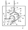
従来から、ミリ波集積回路やミリ波レーダモジュール等に組み込まれて使用される、例えば、図15に模式的な断面図で示すような高周波発振器が知られている。図15に示す高周波発振器は、一端が短絡端51aとして短絡され、他端が出力端51bとして開放された導波管51の中途に設けられた高周波信号を発生するガンダイオード52と、このガンダイオード52にバイアス電圧を印加するためのバイアス供給回路53と、導波管51の短絡端51aとガンダイオード52が設けられた部位との間で構成される共振器54に設けられた、可変容量素子としてのバラクタダイオード55と、このバラクタダイオード55にバイアス電圧を印加するためのバイアス供給回路56とを備えている
そして、従来は、このような高周波発振器に用いられるバイアス供給回路56には、例えば、チップ抵抗等の固定抵抗器が備えられ、その固定抵抗器の抵抗値によりバラクタダイオード55に印加されるバイアス電圧が設定されていた。
Conventionally, for example, a high-frequency oscillator as shown in a schematic cross-sectional view in FIG. 15 that is incorporated in a millimeter-wave integrated circuit, a millimeter-wave radar module, or the like is known. The high-frequency oscillator shown in FIG. 15 has a
このような従来の高周波発振器の例は、バイアス供給回路53によりバイアス電圧をガンダイオード52に印加することによりガンダイオード52からミリ波帯の高周波信号を発生させ、この高周波信号を共振器54で共振させて、例えば77GHzといった周波数の高周波信号を導波管51の出力端51bから出力させることができる。その際、その周波数は、共振器54に設けられたバラクタダイオード55の容量値を変化させることによって変化させることができ、この容量値は、バラクタダイオード55に印加されるバイアス電圧により変化させることができる。すなわち、バイアス供給回路56から出力されてバラクタダイオード55に印加されるバイアス電圧を制御することにより高周波発振器の発振周波数を制御することができ、例えば変調信号として三角波等の電圧信号を発生する変調信号源をバイアス供給回路56に備えることにより、周波数変調された高周波信号として出力させるようにすることができる。
An example of such a conventional high-frequency oscillator is that a bias voltage is applied to the
また、このような従来の高周波発振器の例は、高周波用伝送線路として導波管51の代わりに非放射性誘電体線路(NonRadiative Dielectric Waveguideで、以下、NRDガイドともいう。)を用いてもよく、そのような従来例は例えば特許文献1〜特許文献4に開示されている。
In addition, in the example of such a conventional high-frequency oscillator, a nonradiative dielectric line (hereinafter also referred to as an NRD guide) may be used as a high-frequency transmission line instead of the
この非放射性誘電体線路の基本的な構成は、図16に部分破断斜視図で示すように、所定の間隔aをもって平行配置された平行平板導体61,62の間に、断面形状が長方形等の矩形状の誘電体線路63を配置した構成であり、この間隔aが高周波信号の波長λに対してa≦λ/2であれば、外部から誘電体線路63へのノイズの侵入をなくし、かつ外部への高周波信号の放射をなくして、誘電体線路63中で高周波信号を効率良く伝搬させることができる。なお、高周波信号の波長λは使用周波数における空気中(自由空間)での波長である。
As shown in a partially broken perspective view in FIG. 16, the basic configuration of this non-radiative dielectric line is such that the cross-sectional shape is rectangular between
また、このような従来の高周波発振器は、例えば、特許文献5に開示されているように、高周波信号を送受信する高周波送受信器に組み込まれ、さらにこの高周波送受信器を組み込んだレーダ装置として用いられる。このような高周波送受信器あるいはレーダ装置において、高周波発振器は、例えばミリ波帯の高周波信号を発生させるとともに、この高周波信号に対して特定の周波数範囲で周波数の下限値から上限値まで周波数が上昇と下降とを繰り返すといった周波数変調がなされた高周波信号を出力するように動作する。そして、高周波発振器から出力された高周波信号は、変調器でさらにパルス変調されて送信用高周波信号として送受信アンテナまたは送信アンテナから出力されるように動作する。なお、高周波発振器から出力された高周波信号が送信用高周波信号としてそのまま出力される場合もある。
Such a conventional high-frequency oscillator is incorporated in a high-frequency transmitter / receiver that transmits / receives a high-frequency signal, as disclosed in
また、その他にも従来のレーダ装置およびそれを搭載したレーダ装置搭載車両の例が、例えば、特許文献6に開示されている。
しかしながら、上記従来の高周波発振器や特許文献1〜特許文献4に開示されているような高周波発振器では、高周波発振器の出力端に接続される高周波用伝送線路や他の高周波回路要素の接続状態や動作状態(これらを負荷条件という。)が微妙に異なることにより、発振周波数や周波数変調幅等の発振特性が変化してしまうといったことが起こりやすくて、所望の発振特性を安定して得にくいという問題点があった。
However, in the conventional high-frequency oscillator and high-frequency oscillators disclosed in
また、このような高周波発振器を用いた高周波送受信器では、量産する際に、高周波発振器に接続される高周波回路要素の負荷条件や高周波発振器自身の負荷特性が個々に異なることがあり、組み込まれている高周波発振器が所望の発振特性となりにくいため、良好な送受信性能を安定して得にくいという問題点があった。 In addition, in a high-frequency transmitter / receiver using such a high-frequency oscillator, the load conditions of the high-frequency circuit elements connected to the high-frequency oscillator and the load characteristics of the high-frequency oscillator itself may be different in mass production. The high-frequency oscillator that is used is difficult to achieve desired oscillation characteristics, and thus there is a problem that it is difficult to stably obtain good transmission / reception performance.
本発明は上記事情に鑑みて完成されたものであり、その目的は、高周波発振器の構成要素である可変容量素子のバイアス供給回路により発振周波数や周波数変調幅等の発振特性をチューニングすることができ、良好な発振特性を安定して得ることができる高周波発振器およびそれを用いた高性能な高周波送受信器を提供することにある。 The present invention has been completed in view of the above circumstances, and an object of the present invention is to tune oscillation characteristics such as an oscillation frequency and a frequency modulation width by a bias supply circuit of a variable capacitance element that is a component of a high-frequency oscillator. Another object of the present invention is to provide a high-frequency oscillator capable of stably obtaining good oscillation characteristics and a high-performance high-frequency transceiver using the same.
また、本発明の他の目的は、そのような高性能な高周波送受信器を具備するレーダ装置ならびにそのレーダ装置を備えたレーダ装置搭載車両およびレーダ装置搭載小型船舶を提供することにある。 Another object of the present invention is to provide a radar apparatus equipped with such a high-performance high-frequency transmitter / receiver, a radar apparatus-equipped vehicle equipped with the radar apparatus, and a radar apparatus-equipped small ship.
本発明の高周波発振器は、高周波信号を発生する高周波発振用素子と、この高周波発振用素子に接続された共振器と、この共振器に設けられた、共振周波数を変化させる可変容量素子と、この可変容量素子に接続された、容量を変化させるために印加するバイアス電圧を供給するバイアス供給回路とを具備しており、このバイアス供給回路は、前記バイアス電圧を調節する半固定抵抗器を具備することを特徴とするものである。 The high-frequency oscillator of the present invention includes a high-frequency oscillation element that generates a high-frequency signal, a resonator connected to the high-frequency oscillation element, a variable capacitance element that is provided in the resonator and changes a resonance frequency, A bias supply circuit connected to the variable capacitance element for supplying a bias voltage to be applied to change the capacitance, and the bias supply circuit includes a semi-fixed resistor for adjusting the bias voltage. It is characterized by this.
また、本発明の高周波発振器は、上記構成において、前記半固定抵抗器は、トリマブルチップ抵抗であることを特徴とするものである。 The high-frequency oscillator according to the present invention is characterized in that, in the above configuration, the semi-fixed resistor is a trimmable chip resistor.
また、本発明の高周波発振器は、上記各構成において、前記バイアス供給回路は、前記可変容量素子に試験用のバイアス電圧を印加するための試験用端子を具備することを特徴とするものである。 The high frequency oscillator according to the present invention is characterized in that, in each of the above configurations, the bias supply circuit includes a test terminal for applying a test bias voltage to the variable capacitance element.
本発明の請求項4に係る第1の高周波送受信器は、上記本発明の高周波発振器と、2つの出力端を有し、前記高周波発振器の出力端側に接続され、前記高周波信号を分岐して一方の出力端と他方の出力端とに出力する分岐器と、前記一方の出力端に接続された、この一方の出力端に分岐された高周波信号を変調して送信用高周波信号を出力する変調器と、第1の端子,第2の端子および第3の端子を有し、この順に一つの端子から入力された高周波信号を隣接する次の端子より出力するとともに、前記変調器の出力が前記第1の端子に入力される信号分離器と、この信号分離器の前記第2の端子に接続された送受信アンテナと、前記分岐器の前記他方の出力端と前記信号分離器の前記第3の端子との間に接続された、前記他方の出力端に分岐された高周波信号と前記送受信アンテナで受信した高周波信号とを混合して中間周波信号を出力するミキサーとを具備することを特徴とするものである。 A first high-frequency transmitter / receiver according to a fourth aspect of the present invention includes the high-frequency oscillator according to the present invention and two output ends, and is connected to an output end side of the high-frequency oscillator to branch the high-frequency signal. A branching device that outputs to one output end and the other output end, and a modulation that is connected to the one output end and modulates a high-frequency signal branched to the one output end and outputs a high-frequency signal for transmission And a first terminal, a second terminal, and a third terminal. In this order, a high-frequency signal input from one terminal is output from an adjacent next terminal, and the output of the modulator is A signal separator input to the first terminal; a transmitting / receiving antenna connected to the second terminal of the signal separator; the other output terminal of the branching unit; and the third terminal of the signal separator. Branched to the other output terminal connected between the terminals It is characterized in that it comprises a mixer for outputting the intermediate frequency signal by mixing the radio frequency signal received by the high-frequency signal and the reception antenna.
なお、信号分離器の第3の端子は分岐器の他方の出力端側に接続されているが、この他方の出力端に直接接続されているものではなく、間にミキサーを介して接続されているものである。 The third terminal of the signal separator is connected to the other output end of the branching device, but is not directly connected to the other output end, and is connected via a mixer. It is what.
本発明の請求項5に係る第2の高周波送受信器は、上記本発明の高周波発振器と、2つの出力端を有し、前記高周波発振器の出力端側に接続され、前記高周波信号を分岐して一方の出力端と他方の出力端とに出力する分岐器と、前記一方の出力端に接続された、この一方の出力端に分岐された高周波信号を変調して送信用高周波信号を出力する変調器と、入力端子と出力端子とを有し、前記変調器の出力端に前記入力端子が接続され、前記入力端子側から前記出力端子側へ前記送信用高周波信号を透過させるアイソレータと、このアイソレータの前記出力端子に接続された送信アンテナと、前記分岐器の前記他方の出力端側に接続された受信アンテナと、前記分岐器の前記他方の出力端と前記受信アンテナとの間に接続された、前記他方の出力端に分岐された高周波信号と前記受信アンテナで受信した高周波信号とを混合して中間周波信号を出力するミキサーとを具備することを特徴とするものである。 A second high-frequency transmitter / receiver according to a fifth aspect of the present invention includes the high-frequency oscillator according to the present invention and two output ends, and is connected to an output end side of the high-frequency oscillator to branch the high-frequency signal. A branching device that outputs to one output end and the other output end, and a modulation that is connected to the one output end and modulates a high-frequency signal branched to the one output end and outputs a high-frequency signal for transmission And an isolator having an input terminal and an output terminal, the input terminal being connected to an output end of the modulator, and transmitting the high-frequency signal for transmission from the input terminal side to the output terminal side, and the isolator A transmitting antenna connected to the output terminal, a receiving antenna connected to the other output end of the branching device, and a connection between the other output end of the branching device and the receiving antenna. , Said other out Is characterized in that it comprises a mixer by mixing an RF signal received branched high-frequency signals to an end and at the receiving antenna and outputs an intermediate frequency signal.
本発明の請求項6に係る第3の高周波送受信器は、上記本発明の高周波発振器と、2つの出力端を有し、前記高周波発振器の出力端側に接続され、前記高周波信号を一方の出力端および他方の出力端から選択的に出力する切替え器と、第1の端子,第2の端子および第3の端子を有し、この順に一つの端子から入力された高周波信号を隣接する次の端子より出力するとともに、前記一方の出力端から出力される高周波信号が前記第1の端子に入力される信号分離器と、前記第2の端子に接続された送受信アンテナと、前記他方の出力端と前記第3の端子とに接続され、前記他方の出力端から出力される高周波信号と前記アンテナで受信した高周波信号とを混合して中間周波信号を出力するミキサーとを含むことを特徴とするものである。
A third high-frequency transmitter / receiver according to
本発明の請求項7に係る第4の高周波送受信器は、上記本発明の高周波発振器と、2つの出力端を有し、前記高周波発振器の出力端側に接続され、前記高周波信号を一方の出力端および他方の出力端から選択的に出力する切替え器と、前記一方の出力端に接続された送信アンテナと、受信アンテナと、前記他方の出力端と前記受信アンテナとに接続され、前記他方の出力端から出力される高周波信号と前記受信アンテナで受信した高周波信号とを混合して中間周波信号を出力するミキサーとを含むことを特徴とするものである。 A fourth high-frequency transmitter / receiver according to claim 7 of the present invention has the above-described high-frequency oscillator of the present invention and two output ends, is connected to the output end side of the high-frequency oscillator, and outputs the high-frequency signal to one of the outputs. A switch that selectively outputs from one end and the other output end, a transmission antenna connected to the one output end, a reception antenna, the other output end and the reception antenna, and the other output end And a mixer that mixes the high-frequency signal output from the output terminal with the high-frequency signal received by the receiving antenna and outputs an intermediate frequency signal.
本発明の請求項8に係る第5の高周波送受信器は、上記本発明の高周波発振器と、2つの出力端を有し、前記高周波発振器の出力端側に接続され、前記高周波信号を分岐して一方の出力端と他方の出力端とに出力する分岐器と、第1の端子,第2の端子および第3の端子を有し、この順に一つの端子から入力された高周波信号を隣接する次の端子より出力するとともに、前記分岐器の前記一方の出力端からの出力が前記第1の端子に入力される信号分離器と、この信号分離器の前記第2の端子に接続された送受信アンテナと、前記分岐器の前記他方の出力端と前記信号分離器の前記第3の端子との間に接続され、前記他方の出力端に分岐された高周波信号と前記送受信アンテナで受信した高周波信号とを混合して中間周波信号を出力するミキサーとを具備することを特徴とするものである。
A fifth high-frequency transmitter / receiver according to
本発明の請求項9に係る第6の高周波送受信器は、上記本発明の高周波発振器と、2つの出力端を有し、前記高周波発振器の出力端側に接続され、前記高周波信号を分岐して一方の出力端と他方の出力端とに出力する分岐器と、前記分岐器の前記一方の出力端に接続された送信アンテナと、前記分岐器の前記他方の出力端側に接続された受信アンテナと、前記分岐器の前記他方の出力端と前記受信アンテナとの間に接続された、前記他方の出力端に分岐された高周波信号と前記受信アンテナで受信した高周波信号とを混合して中間周波信号を出力するミキサーとを具備することを特徴とするものである。 A sixth high-frequency transmitter / receiver according to claim 9 of the present invention has the above-described high-frequency oscillator of the present invention and two output ends, and is connected to the output end side of the high-frequency oscillator to branch the high-frequency signal. A branching device that outputs to one output terminal and the other output terminal, a transmission antenna that is connected to the one output terminal of the branching device, and a reception antenna that is connected to the other output terminal side of the branching device A high-frequency signal branched to the other output end connected between the other output end of the branching device and the receiving antenna and a high-frequency signal received by the receiving antenna are mixed to obtain an intermediate frequency And a mixer for outputting a signal.
本発明のレーダ装置は、上記各構成の本発明の第1乃至第6のいずれかの高周波送受信器と、この高周波送受信器から出力される前記中間周波信号を処理して探知対象物までの距離情報を検出する距離情報検出器とを具備することを特徴とするものである。 The radar apparatus according to the present invention includes a high-frequency transmitter / receiver according to any one of the first to sixth aspects of the present invention described above and a distance to a detection target by processing the intermediate frequency signal output from the high-frequency transmitter / receiver. And a distance information detector for detecting information.
本発明のレーダ装置搭載車両は、上記構成の本発明のレーダ装置を備え、このレーダ装置を探知対象物の検出に用いることを特徴とするものである。 The radar device-equipped vehicle of the present invention includes the radar device of the present invention having the above-described configuration, and is characterized in that this radar device is used for detection of an object to be detected.
本発明のレーダ装置搭載小型船舶は、上記構成の本発明のレーダ装置を備え、このレーダ装置を探知対象物の検出に用いることを特徴とするものである。 A small ship equipped with a radar apparatus according to the present invention includes the radar apparatus according to the present invention having the above-described configuration, and is characterized in that this radar apparatus is used for detection of a detection target.
本発明の高周波発振器によれば、高周波信号を発生する高周波発振用素子と、この高周波発振用素子に接続された共振器と、この共振器に設けられた、共振周波数を変化させる可変容量素子と、この可変容量素子に接続された、容量を変化させるために印加するバイアス電圧を供給するバイアス供給回路とを具備しており、このバイアス供給回路は、前記バイアス電圧を調節する半固定抵抗器を具備することから、半固定抵抗器が、発振特性の調整時にはバイアス電圧を適当な値に設定し、それ以外の時にはその一度設定したバイアス電圧の値が保たれるように動作するため、そのバイアス供給回路により適切な容量に調整された可変容量素子によって高周波発振用素子の発振特性が最適となるようにチューニングすることができ、しかもその良好な発振特性を安定に維持することができる高周波発振器となる。 According to the high-frequency oscillator of the present invention, a high-frequency oscillation element that generates a high-frequency signal, a resonator connected to the high-frequency oscillation element, and a variable capacitance element that is provided in the resonator and changes a resonance frequency; And a bias supply circuit connected to the variable capacitance element for supplying a bias voltage to be applied to change the capacitance. The bias supply circuit includes a semi-fixed resistor for adjusting the bias voltage. Therefore, the semi-fixed resistor operates so that the bias voltage is set to an appropriate value when adjusting the oscillation characteristics, and the bias voltage value once set is maintained at other times. The variable capacitance element adjusted to an appropriate capacity by the supply circuit can be tuned to optimize the oscillation characteristics of the high-frequency oscillation element. A high-frequency oscillator that can maintain a good oscillation characteristics stable.
また、本発明の高周波発振器は、上記構成において、前記半固定抵抗器は、トリマブルチップ抵抗であるときには、トリマブルチップ抵抗には可動部分がないため、調整後に外部から振動等の外力が加わっても設定した抵抗値を安定に保つので、良好な発振特性を安定して確実に維持することができる高周波発振器となる。 In the high frequency oscillator of the present invention, in the above configuration, when the semi-fixed resistor is a trimmable chip resistor, since the trimmable chip resistor has no movable part, external force such as vibration is applied from the outside after adjustment. However, since the set resistance value is kept stable, the high-frequency oscillator can stably and reliably maintain good oscillation characteristics.
また、本発明の高周波発振器は、上記各構成において、前記バイアス供給回路は、前記可変容量素子に試験用のバイアス電圧を印加するための試験用端子を具備するときには、試験用端子に試験用の電圧が入力されることにより、高周波送受信器に組み込まれた場合の高周波発振器の可変容量素子に印加すべきバイアス電圧を予め正確に知ることができるため、調整に手間取ることなく半固定抵抗器に設定すべき抵抗値を正確かつ確実に設定することができる高周波発振器となる。また、半固定抵抗器が可逆的に抵抗値を変化させることができないものであっても、設定すべきバイアス電圧の値から半固定抵抗器を設定すべき抵抗値が得られるので、半固定抵抗器を設定すべき抵抗値に確実に設定することができる高周波発振器となる。 The high-frequency oscillator according to the present invention may be configured such that, in each of the above configurations, the bias supply circuit includes a test terminal for applying a test bias voltage to the variable capacitance element. By inputting the voltage, the bias voltage to be applied to the variable capacitor of the high-frequency oscillator when incorporated in the high-frequency transmitter / receiver can be known in advance accurately, so it is set to a semi-fixed resistor without taking the trouble of adjustment. A high-frequency oscillator that can accurately and reliably set the resistance value to be obtained. Even if the semi-fixed resistor cannot change the resistance value reversibly, the resistance value to set the semi-fixed resistor can be obtained from the bias voltage value to be set. It becomes a high frequency oscillator which can set reliably the resistance value which should set a device.
本発明の第1の高周波送受信器によれば、上記本発明の高周波発振器と、2つの出力端を有し、前記高周波発振器の出力端側に接続され、前記高周波信号を分岐して一方の出力端と他方の出力端とに出力する分岐器と、前記一方の出力端に接続された、この一方の出力端に分岐された高周波信号を変調して送信用高周波信号を出力する変調器と、第1の端子,第2の端子および第3の端子を有し、この順に一つの端子から入力された高周波信号を隣接する次の端子より出力するとともに、前記変調器の出力が前記第1の端子に入力される信号分離器と、この信号分離器の前記第2の端子に接続された送受信アンテナと、前記分岐器の前記他方の出力端と前記信号分離器の前記第3の端子との間に接続された、前記他方の出力端に分岐された高周波信号と前記送受信アンテナで受信した高周波信号とを混合して中間周波信号を出力するミキサーとを具備することから、高周波発振器が、高周波送受信器に組み込まれた状態で最適な発振特性にチューニングされて、その良好な発振特性が保たれるように動作するため、良好な送受信性能を安定して得ることができる高周波送受信器となる。また、発振特性が最適に調整されるため、環境条件が変わって発振特性が変化することにより良好な送受信特性が得られなくなるまでのマージンを広くすることができるので、環境条件が変化しても安定な送受信性能を得ることができる高周波送受信器となる。 According to the first high frequency transmitter / receiver of the present invention, the high frequency oscillator of the present invention and two output ends are connected to the output end side of the high frequency oscillator, and the high frequency signal is branched to one output. A branching device that outputs to one end and the other output end; a modulator that is connected to the one output end and that modulates a high-frequency signal branched to the one output end and outputs a high-frequency signal for transmission; A first terminal, a second terminal, and a third terminal; a high-frequency signal input from one terminal in this order is output from an adjacent next terminal; and an output of the modulator is the first terminal A signal separator input to the terminal, a transmission / reception antenna connected to the second terminal of the signal separator, the other output terminal of the branching unit, and the third terminal of the signal separator. High connected to the other output branch Since it has a mixer that mixes the wave signal and the high frequency signal received by the transmission / reception antenna and outputs an intermediate frequency signal, the high frequency oscillator is tuned to the optimum oscillation characteristics in a state of being incorporated in the high frequency transmitter / receiver. Thus, the high-frequency transmitter / receiver can stably obtain a good transmission / reception performance because it operates so as to maintain its good oscillation characteristics. In addition, since the oscillation characteristics are optimally adjusted, it is possible to widen the margin until the favorable transmission / reception characteristics cannot be obtained due to the change in the oscillation characteristics due to the change in the environmental conditions. A high-frequency transmitter / receiver capable of obtaining stable transmission / reception performance is obtained.
本発明の第2の高周波送受信器によれば、上記本発明の高周波発振器と、2つの出力端を有し、前記高周波発振器の出力端側に接続され、前記高周波信号を分岐して一方の出力端と他方の出力端とに出力する分岐器と、前記一方の出力端に接続された、この一方の出力端に分岐された高周波信号を変調して送信用高周波信号を出力する変調器と、入力端子と出力端子とを有し、前記変調器の出力端に前記入力端子が接続され、前記入力端子側から前記出力端子側へ前記送信用高周波信号を透過させるアイソレータと、このアイソレータの前記出力端子に接続された送信アンテナと、前記分岐器の前記他方の出力端側に接続された受信アンテナと、前記分岐器の前記他方の出力端と前記受信アンテナとの間に接続された、前記他方の出力端に分岐された高周波信号と前記受信アンテナで受信した高周波信号とを混合して中間周波信号を出力するミキサーとを具備することから、送受別体のアンテナを用いた高周波送受信器においても、高周波発振器が、高周波送受信器に組み込まれた状態で最適な発振特性にチューニングされて、その良好な発振特性が保たれるように動作するため、良好な送受信性能を安定して得ることができる高周波送受信器となる。また、発振特性が最適に調整されるため、環境条件が変わって発振特性が変化することにより良好な送受信特性が得られなくなるまでのマージンを広くすることができるので、環境条件が変化しても安定な送受信性能を得ることができる高周波送受信器となる。 According to the second high-frequency transmitter / receiver of the present invention, the high-frequency oscillator of the present invention and the two output ends are connected to the output end side of the high-frequency oscillator, and the high-frequency signal is branched to one output. A branching device that outputs to one end and the other output end; a modulator that is connected to the one output end and that modulates a high-frequency signal branched to the one output end and outputs a high-frequency signal for transmission; An isolator having an input terminal and an output terminal, the input terminal being connected to an output end of the modulator, and transmitting the high-frequency signal for transmission from the input terminal side to the output terminal side; and the output of the isolator A transmitting antenna connected to a terminal, a receiving antenna connected to the other output end of the branching device, and the other connected between the other output end of the branching device and the receiving antenna. Minutes at the output end of A mixer that mixes the high-frequency signal received and the high-frequency signal received by the receiving antenna and outputs an intermediate-frequency signal. Since it is tuned to the optimum oscillation characteristics in a state where it is incorporated in the high frequency transmitter / receiver and operates so as to maintain the good oscillation characteristics, it becomes a high frequency transmitter / receiver that can stably obtain good transmission / reception performance. . In addition, since the oscillation characteristics are optimally adjusted, it is possible to widen the margin until the favorable transmission / reception characteristics cannot be obtained due to the change in the oscillation characteristics due to the change in the environmental conditions. A high-frequency transmitter / receiver capable of obtaining stable transmission / reception performance is obtained.
本発明の第3の高周波送受信器によれば、上記本発明の高周波発振器と、2つの出力端を有し、前記高周波発振器の出力端側に接続され、前記高周波信号を一方の出力端および他方の出力端から選択的に出力する切替え器と、第1の端子,第2の端子および第3の端子を有し、この順に一つの端子から入力された高周波信号を隣接する次の端子より出力するとともに、前記一方の出力端から出力される高周波信号が前記第1の端子に入力される信号分離器と、前記第2の端子に接続された送受信アンテナと、前記他方の出力端と前記第3の端子とに接続され、前記他方の出力端から出力される高周波信号と前記アンテナで受信した高周波信号とを混合して中間周波信号を出力するミキサーとを含むことから、高周波発振器が、高周波送受信器に組み込まれた状態で最適な発振特性にチューニングされて、その良好な発振特性が保たれるように動作するため、良好な送受信性能を安定して得ることができる高周波送受信器となる。また、発振特性が最適に調整されるため、環境条件が変わって発振特性が変化することにより良好な送受信特性が得られなくなるまでのマージンを広くすることができるので、環境条件が変化しても安定な送受信性能を得ることができる高周波送受信器となる。 According to the third high-frequency transmitter / receiver of the present invention, the high-frequency oscillator of the present invention and two output ends are connected to the output end side of the high-frequency oscillator, and the high-frequency signal is connected to one output end and the other. A switch that selectively outputs from the output terminal of the first, second, and third terminals, and in this order, a high-frequency signal input from one terminal is output from the next adjacent terminal. And a signal separator for inputting a high-frequency signal output from the one output terminal to the first terminal, a transmission / reception antenna connected to the second terminal, the other output terminal, and the first output terminal. 3 and a mixer that mixes the high-frequency signal output from the other output terminal and the high-frequency signal received by the antenna and outputs an intermediate frequency signal. Transceiver Is tuned to the optimum oscillation characteristic in the installed state, to operate as their good oscillation characteristics is maintained, the high frequency transceiver can be stably obtained with good reception performance. In addition, since the oscillation characteristics are optimally adjusted, it is possible to widen the margin until the favorable transmission / reception characteristics cannot be obtained due to the change in the oscillation characteristics due to the change in the environmental conditions. A high-frequency transmitter / receiver capable of obtaining stable transmission / reception performance is obtained.
本発明の第4の高周波送受信器によれば、上記本発明の高周波発振器と、2つの出力端を有し、前記高周波発振器の出力端側に接続され、前記高周波信号を一方の出力端および他方の出力端から選択的に出力する切替え器と、前記一方の出力端に接続された送信アンテナと、受信アンテナと、前記他方の出力端と前記受信アンテナとに接続され、前記他方の出力端から出力される高周波信号と前記受信アンテナで受信した高周波信号とを混合して中間周波信号を出力するミキサーとを含むことから、送受別体のアンテナを用いた高周波送受信器においても、高周波発振器が、高周波送受信器に組み込まれた状態で最適な発振特性にチューニングされて、その良好な発振特性が保たれるように動作するため、良好な送受信性能を安定して得ることができる高周波送受信器となる。また、発振特性が最適に調整されるため、環境条件が変わって発振特性が変化することにより良好な送受信特性が得られなくなるまでのマージンを広くすることができるので、環境条件が変化しても安定な送受信性能を得ることができる高周波送受信器となる。 According to a fourth high-frequency transmitter / receiver of the present invention, the high-frequency oscillator of the present invention and two output ends are connected to the output end side of the high-frequency oscillator, and the high-frequency signal is sent to one output end and the other. A switch that selectively outputs from the output end of the output terminal, a transmission antenna connected to the one output end, a reception antenna, the other output end and the reception antenna, and from the other output end Since it includes a mixer that mixes a high-frequency signal to be output and a high-frequency signal received by the receiving antenna and outputs an intermediate frequency signal, a high-frequency oscillator using a separate antenna for transmission and reception also includes a high-frequency oscillator, Since it is tuned to the optimum oscillation characteristics when incorporated in a high-frequency transceiver, and operates to maintain its good oscillation characteristics, it is possible to stably obtain good transmission / reception performance. The RF transceiver can. In addition, since the oscillation characteristics are optimally adjusted, it is possible to widen the margin until the favorable transmission / reception characteristics cannot be obtained due to the change in the oscillation characteristics due to the change in the environmental conditions. A high-frequency transmitter / receiver capable of obtaining stable transmission / reception performance is obtained.
本発明の第5の高周波送受信器によれば、上記本発明の高周波発振器と、2つの出力端を有し、前記高周波発振器の出力端側に接続され、前記高周波信号を分岐して一方の出力端と他方の出力端とに出力する分岐器と、第1の端子,第2の端子および第3の端子を有し、この順に一つの端子から入力された高周波信号を隣接する次の端子より出力するとともに、前記分岐器の前記一方の出力端からの出力が前記第1の端子に入力される信号分離器と、この信号分離器の前記第2の端子に接続された送受信アンテナと、前記分岐器の前記他方の出力端と前記信号分離器の前記第3の端子との間に接続された、前記他方の出力端に分岐された高周波信号と前記送受信アンテナで受信した高周波信号とを混合して中間周波信号を出力するミキサーとを具備することから、高周波発振器が、高周波送受信器に組み込まれた状態で最適な発振特性にチューニングされて、その良好な発振特性が保たれるように動作するため、良好な送受信性能を安定して得ることができる高周波送受信器となる。また、発振特性が最適に調整されるため、環境条件が変わって発振特性が変化することにより良好な送受信特性が得られなくなるまでのマージンを広くすることができるので、環境条件が変化しても安定な送受信性能を得ることができる高周波送受信器となる。 According to the fifth high-frequency transmitter / receiver of the present invention, the high-frequency oscillator of the present invention has two output ends, and is connected to the output end side of the high-frequency oscillator to branch the high-frequency signal and output one of them. A branching device that outputs to one end and the other output end, a first terminal, a second terminal, and a third terminal, and a high-frequency signal input from one terminal in this order from an adjacent next terminal And a signal separator in which an output from the one output terminal of the branching device is input to the first terminal, a transmission / reception antenna connected to the second terminal of the signal separator, A high-frequency signal branched to the other output end connected between the other output end of the branching device and the third terminal of the signal separator is mixed with a high-frequency signal received by the transmitting / receiving antenna. And a mixer that outputs an intermediate frequency signal As a result, the high-frequency oscillator is tuned to the optimum oscillation characteristics when incorporated in the high-frequency transceiver, and operates so that the good oscillation characteristics are maintained. It becomes a high frequency transceiver which can be obtained. In addition, since the oscillation characteristics are optimally adjusted, it is possible to widen the margin until the favorable transmission / reception characteristics cannot be obtained due to the change in the oscillation characteristics due to the change in the environmental conditions. A high-frequency transmitter / receiver capable of obtaining stable transmission / reception performance is obtained.
本発明の第6の高周波送受信器によれば、上記本発明の高周波発振器と、2つの出力端を有し、前記高周波発振器の出力端側に接続され、前記高周波信号を分岐して一方の出力端と他方の出力端とに出力する分岐器と、前記分岐器の前記一方の出力端に接続された送信アンテナと、前記分岐器の前記他方の出力端側に接続された受信アンテナと、前記分岐器の前記他方の出力端と前記受信アンテナとの間に接続され、前記他方の出力端に分岐された高周波信号と前記受信アンテナで受信した高周波信号とを混合して中間周波信号を出力するミキサーとを具備することから、送受別体のアンテナを用いた高周波送受信器においても、高周波発振器が、高周波送受信器に組み込まれた状態で最適な発振特性にチューニングされて、その良好な発振特性が保たれるように動作するため、良好な送受信性能を安定して得ることができる高周波送受信器となる。また、発振特性が最適に調整されるため、環境条件が変わって発振特性が変化することにより良好な送受信特性が得られなくなるまでのマージンを広くすることができるので、環境条件が変化しても安定な送受信性能を得ることができる高周波送受信器となる。 According to the sixth high-frequency transmitter / receiver of the present invention, the high-frequency oscillator of the present invention and the two output ends are connected to the output end side of the high-frequency oscillator, and the high-frequency signal is branched to one output. A branching device that outputs to one end and the other output end, a transmission antenna connected to the one output end of the branching device, a receiving antenna connected to the other output end side of the branching device, and The intermediate frequency signal is output by mixing the high frequency signal branched to the other output end and the high frequency signal received by the reception antenna, connected between the other output end of the branching device and the receiving antenna. Because it is equipped with a mixer, even in a high-frequency transmitter / receiver that uses a separate antenna, the high-frequency oscillator is tuned to the optimal oscillation characteristics when incorporated in the high-frequency transmitter / receiver, and its good oscillation To operate as sex is maintained, the high frequency transceiver can be stably obtained with good reception performance. In addition, since the oscillation characteristics are optimally adjusted, it is possible to widen the margin until the favorable transmission / reception characteristics cannot be obtained due to the change in the oscillation characteristics due to the change in the environmental conditions. A high-frequency transmitter / receiver capable of obtaining stable transmission / reception performance is obtained.
本発明のレーダ装置によれば、上記各構成の本発明の第1乃至第6のいずれかの高周波送受信器と、この高周波送受信器から出力される前記中間周波信号を処理して探知対象物までの距離情報を検出する距離情報検出器とを具備することから、高周波送受信器の送受信性能が良好であり、また安定しているため、速く確実に探知対象物を探知することができるとともに至近距離や遠方の探知対象物をも確実に探知することができるレーダ装置となる。 According to the radar apparatus of the present invention, any one of the first to sixth high-frequency transmitter / receivers of the present invention having the above-described configuration and the intermediate frequency signal output from the high-frequency transmitter / receiver are processed to reach a detection target. Because it has a distance information detector for detecting the distance information of the high frequency transmitter / receiver, the transmission / reception performance of the high frequency transmitter / receiver is good and stable, so that the object to be detected can be detected quickly and surely, In other words, the radar apparatus can reliably detect an object to be detected at a long distance.
本発明のレーダ装置搭載車両によれば、上記構成の本発明のレーダ装置を備え、このレーダ装置を探知対象物の検出に用いることから、レーダ装置が速く確実に探知対象物である他の車両や障害物等を探知することができるため、例えばそれらを回避するための急激な挙動を車両に起こさせることなく、車両の適切な制御や運転者への適切な警告をすることができるレーダ装置搭載車両となる。 According to the vehicle equipped with the radar apparatus of the present invention, since the radar apparatus of the present invention having the above-described configuration is provided and this radar apparatus is used for detection of the detection target object, the other radar vehicle is a detection target object quickly and reliably. Radar device that can detect a vehicle and an obstacle, for example, without causing the vehicle to take a sudden action to avoid them, for example, to perform appropriate control of the vehicle and appropriate warning to the driver It becomes an on-board vehicle.
本発明のレーダ装置搭載小型船舶によれば、上記構成の本発明のレーダ装置を備え、このレーダ装置を探知対象物の検出に用いることから、レーダ装置が速く確実に探知対象物である他の小型船舶障害物等を探知することができるため、例えばそれらを回避するための急激な挙動を小型船舶に起こさせることなく、小型船舶の適切な制御や操縦者への適切な警告をすることができるレーダ装置搭載小型船舶となる。 According to the small ship equipped with the radar apparatus of the present invention, the radar apparatus of the present invention having the above-described configuration is provided, and this radar apparatus is used for detection of the detection object. Because small boat obstacles can be detected, for example, appropriate control of small boats and appropriate warnings to pilots can be made without causing the small boats to take a sudden action to avoid them. A small ship equipped with a radar device.
初めに、本発明の高周波発振器およびそれを用いた高周波送受信器について、図面を参照しつつ以下に詳細に説明する。 First, a high-frequency oscillator of the present invention and a high-frequency transceiver using the same will be described in detail below with reference to the drawings.
図1は本発明の高周波発振器の実施の形態の一例における可変容量素子とそのバイアス供給回路を示す模式的なブロック回路図である。また、図2(a)および(b)は、それぞれ図1に示すバイアス供給回路の構成要素であるトリマブルチップ抵抗およびそのトリミング方法の例を示す模式的な平面図および側面図である。また、図3(a)〜(e)は、それぞれ図2に示すトリマブルチップ抵抗における他のトリミング方法の例を示す模式的な平面図である。また、図4および図5は、それぞれ本発明の第1および第2の高周波送受信器の実施の形態の一例を示す模式的なブロック回路図である。また、図6および図7は、それぞれ図4および図5にブロック回路図で示す高周波送受信器の模式的な平面図である。また、図8は図4〜図7に示す高周波送受信器の変調器における高周波変調部の例を示す模式的な斜視図である。また、図9および図10は、それぞれ本発明の第3および第4の高周波送受信器の実施の形態の一例を示す模式的なブロック回路図である。また、図11および図12は、それぞれ本発明の第5および第6の高周波送受信器の実施の形態の一例を示す模式的なブロック回路図である。また、図13は本発明の高周波発振器の実施例におけるトリマブルチップ抵抗のトリミング処理回数とその抵抗値との関係を示す線図である。また、図14は本発明の高周波発振器の実施例におけるトリマブルチップ抵抗の抵抗値と発振周波数との関係を示す線図である。また、図15は高周波発振器の例を示す模式的な断面図である。また、図16は非放射性誘電体線路の基本的な構成を示す部分破断斜視図である。 FIG. 1 is a schematic block circuit diagram showing a variable capacitance element and its bias supply circuit in an example of an embodiment of a high-frequency oscillator according to the present invention. FIGS. 2A and 2B are a schematic plan view and a side view, respectively, showing an example of a trimmable chip resistor that is a component of the bias supply circuit shown in FIG. 1 and a trimming method thereof. 3A to 3E are schematic plan views showing examples of other trimming methods in the trimmable chip resistor shown in FIG. 4 and 5 are schematic block circuit diagrams showing examples of the first and second high-frequency transceivers according to the present invention, respectively. FIGS. 6 and 7 are schematic plan views of the high-frequency transmitter / receiver shown in the block circuit diagrams of FIGS. 4 and 5, respectively. FIG. 8 is a schematic perspective view showing an example of a high-frequency modulation unit in the modulator of the high-frequency transceiver shown in FIGS. 9 and 10 are schematic block circuit diagrams showing examples of the third and fourth high-frequency transceivers according to the present invention, respectively. 11 and 12 are schematic block circuit diagrams showing examples of embodiments of the fifth and sixth high-frequency transceivers of the present invention, respectively. FIG. 13 is a diagram showing the relationship between the number of trimming processings of the trimmable chip resistor and its resistance value in the embodiment of the high frequency oscillator of the present invention. FIG. 14 is a diagram showing the relationship between the resistance value of the trimmable chip resistor and the oscillation frequency in the embodiment of the high frequency oscillator of the present invention. FIG. 15 is a schematic cross-sectional view showing an example of a high-frequency oscillator. FIG. 16 is a partially broken perspective view showing the basic configuration of the non-radiative dielectric line.
図1〜図3において、1は可変容量素子としてのバラクタダイオード、2は半固定抵抗器としてのトリマブルチップ抵抗、3はチョークインダクタ、4は変調信号源、5は試験用端子、2aはトリマブルチップ抵抗2の誘電体基体、2bはトリマブルチップ抵抗2の抵抗体層、2c1,2c2はトリマブルチップ抵抗2の電極、2d,2d1〜2d4は抵抗体層2bのトリミング部である。
1 to 3, 1 is a varactor diode as a variable capacitance element, 2 is a trimmable chip resistor as a semi-fixed resistor, 3 is a choke inductor, 4 is a modulation signal source, 5 is a test terminal, and 2a is a trimmer. The dielectric substrate of the
また、図4〜図12において、11は高周波発振器、12は分岐器(例えば、方向性結合器である。)、13は変調器、14は信号分離器としてのサーキュレータ、15は送受信アンテナ、16はミキサー、17はスイッチ、18はアイソレータ、19は送信アンテナ、20は受信アンテナ、21,31は下側の平板導体、22,32は第1の誘電体線路、23,33は第2の誘電体線路、24,34は磁性体としてのフェライト板、25,35は第3の誘電体線路、26,36は第4の誘電体線路、27,37は第5の誘電体線路、28,38a,38bは無反射終端器、39は第6の誘電体線路、40,44は基板、41はチョーク型バイアス供給線路、42は端子、43は高周波変調用素子、45は高周波検波用素子、12a,71a,73aは入力端、12b,71b,73bは一方の出力端、12c,71c,73cは他方の出力端、13aは入力端、13bは出力端、18aは入力端子、18bは出力端子、14a,24a,34a,72b,75bは第1の端子、14b,24b,34b,72a,75aは第2の端子、14c,24c,34c,72c,75cは第3の端子である。また、71は切替え器としての切替えRFスイッチ、72は信号分離器としての第2の切替えスイッチである。また、73,74はそれぞれ分岐器の構成要素としてのラットレース型ハイブリッド結合器,終端抵抗、75,76はそれぞれ信号分離器の構成要素としての第2のラットレース型ハイブリッド結合器,終端抵抗である。なお、図6および図7において、上側の平板導体は図示していない。
4 to 12, 11 is a high-frequency oscillator, 12 is a branching unit (for example, a directional coupler), 13 is a modulator, 14 is a circulator as a signal separator, 15 is a transmitting / receiving antenna, 16 Is a mixer, 17 is a switch, 18 is an isolator, 19 is a transmission antenna, 20 is a reception antenna, 21 and 31 are lower flat conductors, 22 and 32 are first dielectric lines, and 23 and 33 are second dielectrics. 24, 34 are ferrite plates as magnetic materials, 25, 35 are third dielectric lines, 26, 36 are fourth dielectric lines, 27, 37 are fifth dielectric lines, 28, 38a , 38b are reflection-free terminators, 39 is a sixth dielectric line, 40 and 44 are substrates, 41 is a choke-type bias supply line, 42 is a terminal, 43 is a high-frequency modulation element, 45 is a high-frequency detection element,
また、図15において、51は導波管、52は高周波発振用素子としてのガンダイオード、53,56はバイアス供給回路、54は共振器、55は可変容量素子としてのバラクタダイオード、51aは短絡端、51bは出力端である。また、図16において、61,62は平板導体、63は誘電体線路である。 In FIG. 15, 51 is a waveguide, 52 is a Gunn diode as a high-frequency oscillation element, 53 and 56 are bias supply circuits, 54 is a resonator, 55 is a varactor diode as a variable capacitance element, and 51a is a short-circuited end. , 51b are output terminals. In FIG. 16, 61 and 62 are flat conductors, and 63 is a dielectric line.
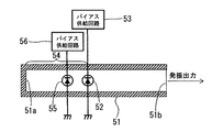
本発明の高周波発振器の実施の形態の一例は、図15および図1に示すように、高周波信号を発生する高周波発振用素子としてのガンダイオード52と、ガンダイオード52に接続された共振器54と、共振器54に設けられた、共振周波数を変化させる可変容量素子としてのバラクタダイオード55(1)と、バラクタダイオード55(1)に接続された、容量を変化させるために印加するバイアス電圧を供給するバイアス供給回路56とを備えており、このバイアス供給回路56は、バイアス電圧を調節する半固定抵抗器としてのトリマブルチップ抵抗2を備えている構成である。
As shown in FIGS. 15 and 1, an example of an embodiment of the high-frequency oscillator of the present invention includes a
また、バイアス供給回路56は、さらにチョークインダクタ3および変調信号源4を備えており、バラクタダイオード1,トリマブルチップ抵抗2,チョークインダクタ3および変調信号源4が直列に接続されている。変調信号源4は、トリマブルチップ抵抗2およびチョークインダクタ3を介してバラクタダイオード1にバイアス電圧を供給する。変調信号源4が供給するバイアス電圧は、一定の直流電圧である。バラクタダイオード1のアノードは接地され、カソードはトリマブルチップ抵抗2に接続される。さらに詳細には、トリマブルチップ抵抗2と変調信号源4との間にチョークインダクタ3が接続される。本実施の形態では、バイアス供給回路10は、正の電圧をバラクタダイオード1に逆バイアスとなるように印加するが、バイアス供給回路10が負の電圧をバラクタダイオード1に逆バイアスとなるように印加する場合には、前記バラクタダイオード1のカソードが接地され、アノードがトリマブルチップ抵抗2に接続される。
The
また、バラクタダイオード1へのバイアス供給回路には、バラクタダイオード1とバイアス供給回路との間に、必ずしも必要ではないが、バラクタダイオード1に並列に試験用のバイアス電圧を印加する電圧源を接続するための試験用端子5が設けられている。さらに詳細には、バラクタダイオード1とトリマブルチップ抵抗2との接続部位に試験用端子5が接続される。試験用端子5に電位を与えることによって、バラクタダイオード1のみに電圧を印加することができる。
Further, in the bias supply circuit to the
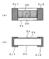
上記構成において、トリマブルチップ抵抗2は、図2に示すように、例えば、アルミナセラミックス等の誘電体から成る誘電体基体2a上にNi−Cr合金等の抵抗体から成る抵抗体層2bが形成されており、この抵抗体層2bの両端に接続されるとともに誘電体基体2aの両端を覆うように電極2c1,2c2が形成されているようなものであり、このトリマブルチップ抵抗2の抵抗体層2bにYAG(イットリウム・アルミニウム・ガーネット)レーザ等からのレーザ光を照射して抵抗体層2bの一部分を適当な面積だけ蒸発させたり、酸化させたりすることでトリミング部2dを形成することにより電極2c1,2c2間の抵抗値を変化させることができるといったものである。例えば、抵抗体層2bの上に抵抗体層2bを保護するとともに、YAGレーザを90%以上通すような絶縁膜を設け、絶縁膜の上から抵抗体層2bの一部を酸化させてトリミング部2dを形成して抵抗値を変化させれば、抵抗体層2bを保護するための工程を別途設ける必要がなくなるため生産性が良好になるとともに、抵抗体層2bが保護されているため、この後の製造工程や周囲の環境等により抵抗値が変化することを防ぐことができるので安定した特性の高周波発振器を得ることができる。
In the above configuration, as shown in FIG. 2, the
そして、高周波発振器において、トリマブルチップ抵抗2は、従来のバイアス供給回路56においてチップ抵抗等の固定抵抗器を用いていた場合と同様に、その抵抗値によりバラクタダイオード1(55)に印加される電圧を適当な値に設定し、バラクタダイオード1(55)に適当な容量値を設定することにより適当な発振周波数や周波数変調幅等の発振特性が得られるといった働きをする。ただし、トリマブルチップ抵抗2は、チップ抵抗等の固定抵抗器とは異なり、高周波発振器を高周波送受信器に組み込む際に既にそれが一括リフロー工程等によって高周波発振器の構成要素として接続されていたとしても、トリマブルチップ抵抗2の抵抗値をトリミング等の方法によって調整することにより負荷条件に適応させて発振特性のチューニングを実施することができる。なお、通常は、負荷条件である高周波発振器の出力端51bから出力端51bに接続される高周波回路要素側を見たインピーダンスが様々であったり、ガンダイオード51の負荷特性が様々であったりするので、トリマブルチップ抵抗2の抵抗値を調整することにより負荷条件に適応させて発振特性のチューニングを実施することによって、大量に生産される高周波発振器11における発振特性を揃えることができるとともに、所望の発振特性を得ることができるようになるので歩留まりを向上させることができる。
In the high-frequency oscillator, the
なお、上記のようなトリマブルチップ抵抗2の働きは、トリマブルチップ抵抗2の他にも、回転方式や接点方式等の機械式のトリマ抵抗やポテンショメータ等の半固定抵抗器を用いても同様に得ることができるが、トリマブルチップ抵抗2は、振動が加わっても抵抗値がずれない点や、温度や湿度に対する信頼性が高い点で好ましい。
The function of the
このトリマブルチップ抵抗2は、具体的には次のように使用すればよい。すなわち、図2に示すように、抵抗体層2bの電極2c1,2c2が接続されていない周辺部の外側から内側に向かって例えばYAGレーザ光を照射して、直線状の切り込み(直線状カット)を入れてトリミング部2dを形成すればよい。この直線状カット等のトリミング部2dの面積によりトリマブルチップ抵抗2の抵抗値が変わり、この面積を大きくするに従って抵抗体層2bの断面において電流が流れる断面積が小さくなるため、その抵抗値を大きくすることができる。通常は、所望の調整範囲で抵抗値の初期値が小さめのものを選定し、その抵抗値を大きくする方向で調整するようにすればよい。また、直線状カットによってトリミング部2dの面積を広げる際には、幅はYAGレーザ光のスポットサイズで決まる一定の大きさとしておいて、そのYAGレーザ光を一軸方向に走査するようにしてその走査する方向にその面積を広げるようにすればよい。また、その際、次の走査をする前に同じ部位で複数回、パルス状のYAGレーザ光を照射すればよい。このようにすれば抵抗値の調整(トリミング)を高精度で行なうことができる。
Specifically, the
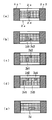
また、図2に示すような直線状カットの他にも、図3(a)に平面図で示すように、上記のような直線状カットを抵抗体層2bの中央部にいわゆる島状に設けたトリミング部2dとしてもよい。また、図3(b)に同様に示すように、上記のような直線状カットを第1カット2d1として設けた後、同様の直線状カットを第2カット2d2として第1カット2d1から少し離れた位置に第1カット2d1よりも短い長さで設けてもよい(ダブルカット)。また、図3(c)に同様に示すように、そのようなダブルカットに対して、第1カット2d1を設けた辺に対向する辺に第2カット2d2を設けるようにしたダブルカットとしてもよい。また、図3(d)に同様に示すように、図3(c)に示すようなダブルカット2d1,2d2と、これと同様のダブルカット2d3,2d4とを櫛歯状に設けてもよい(サーペンタインカット)。図3(b)〜(d)に示すようにトリミング部2d,2d1〜2d4を形成すれば、第2カット2d2,2d4によってより緻密に抵抗値を設定することができるため、より高精度なトリミングによる調整を行なうことができる。特に、図3(d)に示すように、櫛歯状にカット部2d1〜2d4を設けるときには、抵抗体層2bの線路長を長くすることができるので抵抗値を広い範囲で調整することができるので好ましい。
In addition to the linear cut as shown in FIG. 2, as shown in the plan view of FIG. 3A, the linear cut as described above is provided in the so-called island shape at the center of the resistor layer 2b. The trimming
また、図3(e)に同様に示すように、直線状カットに対して走査する方向を途中でほぼ直角に曲げたL字状の切り込み(Lカット)を設けてもよい。この場合には、抵抗体層2bにかかる応力が緩和されて抵抗体層2bにマイクロクラックが入りにくくなり、マイクロクラックの影響による抵抗値のドリフトを小さくすることができる。 Further, as similarly shown in FIG. 3E, an L-shaped cut (L cut) may be provided in which the scanning direction with respect to the linear cut is bent at a substantially right angle in the middle. In this case, the stress applied to the resistor layer 2b is relaxed, and microcracks are less likely to enter the resistor layer 2b, and the drift of the resistance value due to the influence of the microcracks can be reduced.
なお、このようなトリマブルチップ抵抗2は、1つでも十分な調整幅のトリミングが可能なものであるが、これを複数個直列や並列に接続する等したものを用いても構わない。
Although such a
このようなトリマブルチップ抵抗2は、高周波発振器11を高周波送受信器に組み付けたときに、外部に露出するように設けられる。これによって高周波送受信器に高周波発振器11を組み付けた状態で、トリマブルチップ抵抗2の抵抗値を変化させることができる。
Such a
本発明の高周波発振器の実施の形態の一例によれば、上記構成とすることから、半固定抵抗器としてのトリマブルチップ抵抗2が、発振特性の調整時にはバイアス電圧を適当な値に設定し、それ以外の時、例えば、高周波発振器を高周波送受信器などの製品に組み込んだ時にはその一度設定したバイアス電圧の値が保たれるように動作するため、このトリマブルチップ抵抗2を具備するバイアス供給回路により適切な容量に調整された可変容量素子によって高周波発振用素子の発振特性が最適となるようにチューニングすることができ、しかもその良好な発振特性を安定に維持することができる。また、トリマブルチップ抵抗2には可動部分がないため、調整後に外部から振動等の外力が加わっても設定した抵抗値を安定に保つので、良好な発振特性を安定して確実に維持することができる。
According to an example of the embodiment of the high-frequency oscillator of the present invention, because of the above configuration, the
なお、本発明でいう半固定抵抗器とは、抵抗値を可変に設定することができて、かつ設定した抵抗値が不用意に変動しない特性を持ち合わせたものということであって、特に抵抗値の調整回数の仕様については、例えば少なくとも数十回程度の調整に耐えられるようなものであれば、それ以上は如何様であっても構わない。 The semi-fixed resistor in the present invention means that the resistance value can be variably set and the set resistance value has characteristics that do not fluctuate carelessly. As for the specification of the number of adjustments, for example, any number may be used as long as it can withstand at least several tens of adjustments.
また、本発明の高周波発振器の実施の形態の一例によれば、バラクタダイオード1とバイアス供給回路との間に、バラクタダイオード1に並列に試験用のバイアス電圧を印加する電圧源を接続するための試験用端子5が設けられているときには、試験用端子5に試験用のバイアス電圧が印加されることにより、バラクタダイオード1に印加すべきバイアス電圧を予め正確に知ることができるため、それに基づいて、調整に手間取ることなくトリマブルチップ抵抗2に設定すべき抵抗値を正確かつ確実に設定することができる。また、半固定抵抗器がトリマブルチップ抵抗2のように可逆的に抵抗値を変化させることができないものであっても、設定すべきバイアス電圧の値からトリマブルチップ抵抗2に設定すべき抵抗値が前もって得られるので、トリマブルチップ抵抗2に設定すべき抵抗値を確実に設定することができる。なお、このような試験をしなくても過去のデータ等から設定すべき抵抗値が得られるような場合には、必ずしも試験用端子5を設ける必要はない。
According to an example of the embodiment of the high-frequency oscillator of the present invention, a voltage source for applying a test bias voltage in parallel to the
なお、通常、バラクタダイオード1の容量値は印加されるバイアス電圧の電圧値に対して非線形に変化するが、周波数変調において周波数を変化させる幅(周波数変調幅)を一定としたいようなときには、変調信号源の振幅を調整するようにトリマブルチップ抵抗2を用いてもよい。具体的には、変調信号を出力する例えば差動増幅器を構成する演算増幅器(オペアンプ)の帰還回路である反転入力端子もしくは非反転入力端子と出力端子との間に接続される抵抗に、上記のようなトリマブルチップ抵抗2を用いればよい。このようにすれば、周波数変調の中心周波数を調整した上で周波数変調幅をも調整することができるものとなる。
Normally, the capacitance value of the
なお、本発明の高周波発振器においては、高周波用伝送線路として、導波管51の他にも、ストリップ線路,マイクロストリップ線路,コプレーナ線路,グランド付きコプレーナ線路,スロット線路,誘電体導波管,非放射性誘電体線路等を用いてもよい。
In the high-frequency oscillator of the present invention, in addition to the
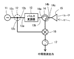
次に、図4に示す本発明の第1の高周波送受信器の実施の形態の一例は、上記本発明の高周波発振器である高周波発振器11と、2つの出力端12b,12cを有し、高周波発振器11の出力端側に接続され、高周波信号を分岐して一方の出力端12bと他方の出力端12cとに出力する分岐器12と、一方の出力端12bに接続された、この一方の出力端12bに分岐された高周波信号を変調して送信用高周波信号を出力する変調器13と、磁性体の周囲に第1の端子14a,第2の端子14bおよび第3の端子14cを有し、この順に一つの端子から入力された高周波信号を隣接する次の端子より出力するとともに、変調器13の出力が第1の端子14aに入力される信号分離器としてのサーキュレータ14と、このサーキュレータ14の第2の端子14bに接続された送受信アンテナ15と、分岐器12の他方の出力端12cとサーキュレータ14の第3の端子14cとの間に接続された、他方の出力端12cに分岐された高周波信号と送受信アンテナ15で受信した高周波信号とを混合して中間周波信号を出力するミキサー16とを備えている構成である。
Next, an example of an embodiment of the first high-frequency transmitter / receiver of the present invention shown in FIG. 4 has a high-
また、図5に示す本発明の第2の高周波送受信器の実施の形態の一例は、上記本発明の高周波発振器である高周波発振器11と、2つの出力端12b,12cを有し、高周波発振器11の出力端側に接続され、高周波信号を分岐して一方の出力端12bと他方の出力端12cとに出力する分岐器12と、一方の出力端12bに接続された、この一方の出力端12bに分岐された高周波信号を変調して送信用高周波信号を出力する変調器13と、入力端子18aと出力端子18bとを有し、変調器13の出力端13bに入力端子18aが接続された、入力端子18a側から出力端子18b側へ送信用高周波信号を透過させるアイソレータ18と、このアイソレータ18に接続された送信アンテナ19と、分岐器12の他方の出力端12c側に接続された受信アンテナ20と、分岐器12の他方の出力端12cと受信アンテナ20との間に接続された、他方の出力端12cに分岐された高周波信号と受信アンテナ20で受信した高周波信号とを混合して中間周波信号を出力するミキサー16とを備えている構成である。
An example of the second high-frequency transceiver according to the present invention shown in FIG. 5 includes the high-
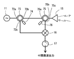
また、図9に示す本発明の第3の高周波送受信器の実施の形態の一例は、上記本発明の高周波発振器である高周波発振器11と、2つの出力端71b,71cを有し、高周波発振器11の出力端側に接続され、高周波信号を一方の出力端71bに送信用高周波信号RFtを、他方の出力端71cからローカル信号LOを切替えて選択的に出力する切替え器としてのRFスイッチ71と、第1の端子としての入力端72b、第3の端子としての出力端72cおよび第2の端子としての入出力端72aを有し、一方の出力端71bに入力端72bが接続され、入出力端72aを入力端72bまたは出力端72cに切り替えて接続する信号分離器としての第2の切替えRFスイッチ72と、入出力端(第2の端子)72aに接続された送受信アンテナ15と、他方の出力端71cと出力端(第3の端子)72cとに接続され、他方の出力端71cから出力される高周波信号(ローカル信号)LOとアンテナ15で受信した高周波信号RFrとを混合して中間周波信号を出力するミキサー16とを備えている構成である。
An example of the embodiment of the third high-frequency transmitter / receiver of the present invention shown in FIG. 9 has a high-
言い換えると、信号分離器である第2の切替えRFスイッチ72は、第1の端子72b、第2の端子72aおよび第3の端子72cを有し、第1の端子72b、第2の端子72aおよび第3の端子72c間の接続状態を切替えることによって、第1の端子72bに切替RFスイッチ71から送信用高周波信号が与えられ、第1の端子72bから入力される高周波信号を第2の端子72aから出力し、第2の端子72aから入力される高周波信号を第3の端子72cから出力する。
In other words, the second switching RF switch 72, which is a signal separator, has a
また、図10に示す本発明の第4の高周波送受信器の実施の形態の一例は、上記本発明の高周波発振器である高周波発振器11と、2つの出力端71b,71cを有し、高周波発振器11の出力端側に接続され、高周波信号を分岐して一方の出力端71bに送信用高周波信号RFtを、他方の出力端71cからローカル信号LOを切替えて選択的に出力する切替え器としてのRFスイッチ71と、一方の出力端71bに接続された送信アンテナ19と、受信アンテナ20と、切替えRFスイッチ71の他方の出力端71cと受信アンテナ20との間に接続され、他方の出力端71cに出力された高周波信号(ローカル信号)LOと受信アンテナ20で受信した高周波信号RFrとを混合して中間周波信号を出力するミキサー16とを備えている構成である。
An example of the embodiment of the fourth high-frequency transmitter / receiver of the present invention shown in FIG. 10 includes the high-
また、図11に示す本発明の第5の高周波送受信器の実施の形態の一例は、上記本発明の高周波発振器である高周波発信器11と、2つの出力端73b,73cを有し、高周波発振器11の出力端側に接続され、高周波信号を分岐して一方の出力端73bと他方の出力端73cとに出力する分岐器としてのラットレース型ハイブリッド結合器73および一方の出力端73bと他方の出力端73cとの間に接続された終端抵抗74(ラットレース型ハイブリッド結合器73と終端抵抗74とで分岐器を構成する。)と、第1の端子75a,第2の端子75bおよび第3の端子75cを有し、この順に一つの端子から入力された高周波信号を隣接する次の端子より出力するとともに、第1の端子75aが一方の出力端73bに接続されてラットレース型ハイブリッド結合器73で分岐された高周波信号が第1の端子75aに入力される第2のラットレース型ハイブリッド結合器75および第1の端子75aと第3の端子75cとの間に接続された終端抵抗76(第2のラットレース型ハイブリッド結合器75と終端抵抗とで信号分離器を構成する。)と、この第2のラットレース型ハイブリッド結合器75の第2の端子75bに接続された送受信アンテナ15と、ラットレース型ハイブリッド結合器73の他方の出力端73cと第2のラットレース型ハイブリッド結合器75の第3の端子75cとの間に接続され、他方の出力端73cに分岐された高周波信号と送受信アンテナ15で受信した高周波信号とを混合して中間周波信号を出力するミキサー16とを備えている構成である。
Further, an example of the fifth high-frequency transmitter / receiver according to the present invention shown in FIG. 11 includes the high-
また、図12に示す本発明の第6の高周波送受信器の実施の形態の一例は、上記本発明の高周波発振器である高周波発信器11と、2つの出力端73b,73cを有し、高周波発振器11の出力端側に接続され、高周波信号を分岐して一方の出力端73bと他方の出力端73cとに出力する分岐器としてのラットレース型ハイブリッド結合器73および一方の出力端73bと他方の出力端73cとの間に接続された終端抵抗74(ラットレース型ハイブリッド結合器73と終端抵抗74とで分岐器を構成する。)と、ラットレース型ハイブリッド結合器73の一方の出力端73bに接続された送信アンテナ19と、ラットレース型ハイブリッド結合器73の他方の出力端73c側に接続された受信アンテナ20と、ラットレース型ハイブリッド結合器73の他方の出力端73cと受信アンテナ20との間に接続された、他方の出力端73cに分岐された高周波信号と受信アンテナ20で受信した高周波信号とを混合して中間周波信号を出力するミキサー16とを備えている構成である。
An example of the sixth high-frequency transmitter / receiver according to the present invention shown in FIG. 12 includes the high-
また、上記各構成に対して、好ましくは、ミキサー16の出力端には、外部からの開閉制御信号に応じて中間周波信号を開閉(スイッチング)するスイッチ17を設けるとよい。
In addition, for each of the above-described configurations, a
このような図4,図5,図9,図10,図11,図12に示す高周波送受信器は、従来の高周波送受信器と同様に動作するが、所望の発振特性を得るところの負荷条件が個別に変動しても、高周波発振器がそれら個々の負荷条件に応じて発振特性をチューニングする働きをするため、所定の周波数および出力の送信用高周波信号を安定に出力することができる。 4, 5, 9, 10, 11, and 12 operate in the same manner as a conventional high frequency transmitter / receiver. However, the load condition for obtaining a desired oscillation characteristic is as follows. Even if it fluctuates individually, the high-frequency oscillator functions to tune the oscillation characteristics in accordance with the individual load conditions, so that it is possible to stably output a transmission high-frequency signal having a predetermined frequency and output.
また、ミキサー16の出力端に、外部からの開閉制御信号に応じて中間周波信号を開閉(スイッチング)するスイッチ17を設けたときには、信号分離器としてのサーキュレータ14の第1の端子14aと第3の端子14cとの間,信号分離器としての第2のRFスイッチ72の第1の端子72bと第3の端子72cとの間,信号分離器としての第2のラットレース型ハイブリッド結合器75の第1の端子75aと第3の端子75cとの間または送信アンテナ19と受信アンテナ20との間のアイソレーションの不足等で、サーキュレータ14の第3の端子14c,第2のRFスイッチ72の第3の端子72c,第2のラットレース型ハイブリッド結合器75の第3の端子75cまたは受信アンテナ20に送信用高周波信号の一部が漏洩したとしても、この漏洩した高周波信号に対する中間周波信号を出力させないように、スイッチ17がそのような中間周波信号を遮断するように動作させることができるので、受信すべき高周波信号を受信側で識別しやすくすることができる。
Further, when a
また、さらに具体的には、図4および図5のそれぞれに示す本発明の第1および第2の高周波送受信器は、上記各構成要素間を接続して高周波信号を伝送するための高周波用伝送線路として、非放射性誘電体線路を用いている。この非放射性誘電体線路の基本的な構成は、図16に部分破断斜視図で示すものと同様である。 More specifically, the first and second high-frequency transmitter / receivers of the present invention shown in FIGS. 4 and 5 respectively transmit high-frequency signals by connecting the above constituent elements to transmit high-frequency signals. A non-radiative dielectric line is used as the line. The basic configuration of this nonradiative dielectric line is the same as that shown in the partially broken perspective view of FIG.
すなわち、図4にブロック回路図で示す本発明の第1の高周波送受信器は、図6に平面図で示すように、高周波信号の波長の2分の1以下の間隔で平行に配置された平板導体21(他方の平板導体は図示していない。)間に、第1の誘電体線路22の一端が接続された、高周波ダイオードから出力された高周波信号を周波数変調するとともに第1の誘電体線路22を伝搬させて出力する上記本発明の高周波発振器11と、第1の誘電体線路22の他端に接続された、その高周波信号をパルス信号に応じて入力端13a側に反射するかまたは出力端13b側に透過させる変調器13と、変調器13の出力端13bに一端が接続された第2の誘電体線路23と、平板導体21に平行に配設されたフェライト板24の周縁部に、それぞれ高周波信号の入出力端子とされた第1の端子24a,第2の端子24bおよび第3の端子24cを有し、この順に、一つの端子から入力された高周波信号を隣接する次の端子より出力する、第1の端子24aが第2の誘電体線路23の他端に接続されたサーキュレータ14と、サーキュレータ14のフェライト板24の周縁部に放射状に配置され、かつ第2の端子24bおよび第3の端子24cにそれぞれの一端が接続された第3の誘電体線路25および第4の誘電体線路26と、第3の誘電体線路25の他端に接続された送受信アンテナ15と、中途を第1の誘電体線路22の中途に近接もしくは接合させた、第1の誘電体線路22を伝搬する高周波信号の一部を分岐して伝搬させる第5の誘電体線路27と、第5の誘電体線路27の高周波発振器11側の一端に接続された無反射終端器28と、第4の誘電体線路26の他端と第5の誘電体線路27の他端との間に接続された、第5の誘電体線路27から入力される高周波信号と送受信アンテナ15で受信してサーキュレータ14から入力される高周波信号とを混合して中間周波信号を出力するミキサー16とを備えている。なお、第1の誘電体線路22および第5の誘電体線路27は、それらの近接部もしくは接合部において分岐器12を構成している。
That is, the first high-frequency transmitter / receiver of the present invention shown in the block circuit diagram of FIG. 4 is a flat plate arranged in parallel at intervals of 1/2 or less of the wavelength of the high-frequency signal as shown in the plan view of FIG. One end of the first
また、図5にブロック回路図で示す本発明の第2の高周波送受信器は、図7に平面図で示すように、高周波信号の波長の2分の1以下の間隔で平行に配置された平板導体31(他方の平板導体は図示していない。)間に、第1の誘電体線路32の一端が接続された、高周波ダイオードから出力された高周波信号を周波数変調するとともに第1の誘電体線路32を伝搬させて出力する上記本発明の高周波発振器11と、第1の誘電体線路32の他端に接続された、その高周波信号をパルス信号に応じて入力端13a側に反射するかまたは出力端13b側に透過させる変調器13と、変調器13の出力端13bに一端が接続された第2の誘電体線路33と、平板導体31に平行に配設されたフェライト板34の周縁部に、それぞれ高周波信号の入出力端子とされた第1の端子34a,第2の端子34bおよび第3の端子34cを有し、この順に、一つの端子から入力された高周波信号を隣接する次の端子より出力する、第1の端子34aが第2の誘電体線路33の他端に接続されたサーキュレータ14と、サーキュレータ14のフェライト板34の周縁部に放射状に配置され、かつ第2の端子34bおよび第3の端子34cにそれぞれの一端が接続された第3の誘電体線路35および第4の誘電体線路36と、第3の誘電体線路35の他端に接続された送信アンテナ19と、中途を第1の誘電体線路32の中途に近接もしくは接合させた、第1の誘電体線路32を伝搬する高周波信号の一部を分岐して伝搬させる第5の誘電体線路37と、第4の誘電体線路36の他端に接続された無反射終端器38aと、第5の誘電体線路37の高周波発振器11側の一端に接続された無反射終端器38bと、一端が受信アンテナ20に接続された第6の誘電体線路39と、第5の誘電体線路37の他端と第6の誘電体線路39の他端との間に接続された、第5の誘電体線路37から入力される高周波信号と受信アンテナ20で受信して第6の誘電体線路39から入力される高周波信号とを混合して中間周波信号を出力するミキサー16とを備えている。なお、第1の誘電体線路32および第5の誘電体線路37は、それらの近接部もしくは接合部において分岐器12を構成している。
Further, the second high-frequency transmitter / receiver of the present invention shown in the block circuit diagram of FIG. 5 is a flat plate arranged in parallel at an interval of 1/2 or less of the wavelength of the high-frequency signal as shown in the plan view of FIG. One end of the first
なお、図6において、第1の端子24a,第2の端子24b,第3の端子24cは、それぞれ図4における第1の端子14a,第2の端子14b,第3の端子14cに対応している。また、図7において、第1の端子34a,第2の端子34b,第3の端子34cは、それぞれ図5における第1の端子14a,第2の端子14b,第3の端子14cに対応している。
In FIG. 6, the
これらの構成において、変調器13は、図8に斜視図で示すように、基板40の表面に形成されたチョーク型バイアス供給線路41の途中の途切れた部位に形成された接続端子42に高周波変調用素子としてのダイオード43を接続した高周波変調部を、第1の誘電体線路22,32と第2の誘電体線路23,33との間に、第1の誘電体線路22,32から出力される高周波信号がダイオード43に入射するように挿入している。この構成において、高周波変調用素子としてのダイオード43には、PINダイオードを用いればよい。また、ダイオード43の代わりにトランジスタやマイクロ波モノリシック集積回路(MMIC)を用いても構わない。
In these configurations, as shown in a perspective view in FIG. 8, the
本発明の高周波送受信器における変調器13には、このような透過形の変調器が好適である。また、透過型の変調器の代わりに、高周波信号を透過させたり反射したりすることができる半導体スイッチやMEMS(Micro Electro Mechanical System:微小電気機械システム)スイッチ等のスイッチを用いてもよい。
Such a transmission type modulator is suitable for the
また、本発明の高周波発振器は、このような変調器13を用いた高周波送受信器の他に、そのような変調器13を用いないものに対しても有効である。この場合には、上記本発明の第1および第2の高周波送受信器に対して、変調器13を取り除き、第1の誘電体線路22,32の入力端13a側の端部と第2の誘電体線路23,33の出力端13b側の端部とを接続するようにすればよい。
Further, the high frequency oscillator of the present invention is effective not only for a high frequency transmitter / receiver using such a
また、ミキサー16は、図8に示すものと同様の2つの基板44のそれぞれに高周波検波用素子としてのダイオード45を設けた高周波検波部を、第4の誘電体線路26(第5の誘電体線路37)および第5の誘電体線路27(第6の誘電体線路39)のそれぞれに、第4の誘電体線路26(第5の誘電体線路37)および第5の誘電体線路27(第6の誘電体線路39)のそれぞれから出力された高周波信号が各ダイオード45に入射するように接続し、かつ第4の誘電体線路26と第5の誘電体線路27と(第5の誘電体線路37と第6の誘電体線路39と)が電磁結合するように、第4の誘電体線路26の中途と第5の誘電体線路27の中途と(第5の誘電体線路37の中途と第6の誘電体線路39の中途と)を近接させるかまたは接合させている。この構成において、高周波検波用素子としてのダイオード45には、ショットキーバリアダイオードを用いればよい。また、ダイオード45の代わりにトランジスタやマイクロ波モノリシック集積回路(MMIC)を用いても構わない。
Further, the
また、第1および第2の高周波送受信器においては、信号分離器としてサーキュレータ14を用いた例について説明したが、サーキュレータ14の代わりのものとして、デュプレクサ,スイッチまたはハイブリッド回路等を用いても構わない。なお、ハイブリッド回路には、上記第2のラットレース型ハイブリッド結合器75の他、ブランチライン型ハイブリッド回路等も含まれる。
In the first and second high-frequency transmitter / receivers, the example in which the
このように、高周波用伝送線路として非放射性誘電体線路を用いて高周波送受信器を構成すれば、高周波送受信器の内部において高周波信号を低損失に伝送することができるため、安定した送受信性能を得ることができる。また、送信用高周波信号の出力を大きくすることができるため、受信側に複雑な増幅回路を必要としないという利点がある。 Thus, if a high frequency transmitter / receiver is configured using a non-radiative dielectric line as a high frequency transmission line, a high frequency signal can be transmitted with low loss inside the high frequency transmitter / receiver, so that stable transmission / reception performance is obtained. be able to. Further, since the output of the high-frequency signal for transmission can be increased, there is an advantage that a complicated amplifier circuit is not required on the receiving side.
図4〜図7にブロック回路図および平面図で示す本発明の第1および第2の高周波送受信器の実施の形態の例は、高周波発振器11が、高周波送受信器に組み込まれた状態で最適な発振特性にチューニングされて、その良好な発振特性が保たれるように動作するため、良好な送受信性能を安定して得ることができるものとなる。また、発振特性が最適に調整されるため、環境条件が変わって発振特性が変化することにより良好な送受信特性が得られなくなるまでのマージンを広くすることができるので、環境条件が変化しても安定な送受信性能を得ることができるものとなる。
The first and second embodiments of the first and second high-frequency transceivers according to the present invention shown in the block circuit diagrams and plan views in FIGS. 4 to 7 are optimal when the high-
次に、本発明の第1および第2の高周波送受信器の構成要素について詳細に説明する。 Next, the components of the first and second high-frequency transceivers of the present invention will be described in detail.
本発明の第1および第2の高周波送受信器において、第1〜第6の誘電体線路22,23,25,26,27,32,33,35,36,37,39の材質には、四フッ化エチレン,ポリスチレン等の樹脂、または低比誘電率のコーディエライト(2MgO・2Al2O3・5SiO2)セラミックス,アルミナ(Al2O3)セラミックス,ガラスセラミックス等のセラミックスが好ましく、これらはミリ波帯域において低損失である。
In the first and second high-frequency transmitter / receivers of the present invention, the first to sixth
また、第1〜第6の誘電体線路22,23,25,26,27,32,33,35,36,37,39の断面形状は基本的には矩形状であるが、矩形の角部を丸めた形状であってもよく、高周波信号の伝送に使用される種々の断面形状のものを使用することができる。
The first to sixth
また、フェライト板24,34の材質には、フェライトの中でも、例えばミリ波信号に対しては、亜鉛・ニッケル・鉄酸化物(ZnaNibFecOx)が好適である。
As the material of the
また、フェライト板24,34の形状は、通常は円板状とされるが、その他、平面形状が正多角形状であってもよい。その場合は、接続される誘電体線路の本数をn本(nは3以上の整数)とすると、その平面形状は正m角形(mは3以上のnより大きい整数)とするのがよい。
In addition, the shape of the
また、無反射終端器28,38a,38bは、それら無反射終端器28,38a,38bが接続される第5の誘電体線路27,第4および第5の誘電体線路36,37の端部に対して、両側の側面(平板導体21,31および図示していない他方の平板導体の内面と対向しない面)の上下端部に、膜状の抵抗体または電波吸収体を付着させて構成すればよい。その際、抵抗体の材質としては、ニッケルクロム合金またはカーボンが好適である。また、電波吸収体の材質としては、パーマロイまたはセンダストが好適である。これらの材質を用いれば、効率良く高周波信号を減衰させることができる。また、これら以外の材質で、高周波信号を減衰させることができるものを用いても構わない。
The
また、平板導体21,31および図示していない他方の平板導体の材質には、高い電気伝導度および良好な加工性等の点で、Cu,Al,Fe,Ag,Au,Pt,SUS(ステンレススチール),真鍮(Cu−Zn合金)等の導体板が好適である。あるいは、セラミックス,樹脂等から成る絶縁板の表面にこれらの導体層を形成したものでもよい。
Further, the materials of the
なお、本発明の第3〜第6の高周波送受信器においても、図4〜図8に示す高周波送受信器の例と同様に、高周波用伝送線路としては非放射性誘電体線路,誘電体導波管線路,導波管,誘電体導波管,ストリップ線路,マイクロストリップ線路,コプレーナ線路およびスロット線路等を用いればよい。 In the third to sixth high-frequency transmitter / receivers of the present invention, as in the example of the high-frequency transmitter / receiver shown in FIGS. 4 to 8, as the high-frequency transmission line, a non-radiative dielectric line and a dielectric waveguide are used. A line, a waveguide, a dielectric waveguide, a strip line, a microstrip line, a coplanar line, a slot line, or the like may be used.
また、切替えRFスイッチ71および第2の切替えRFスイッチ72としては上記変調器13の例と同様のものを用いればよい。具体的には、上記第1および第2の高周波送受信器における変調器13は、透過特性を変えることでオン/オフを切替えてパルス変調させていたが、第3および第4の高周波送受信器においては、上記変調器13を、オン/オフの切替えをさせていたものから、入力端71aから出力端71bまたは出力端71cへの接続状態の切替え,第2の端子72aから第1の端子72bまたは第3の端子72cへの接続状態の切替えをさせるものとする。このようなRFスイッチ71は、第1および第2の高周波送受信器における分岐器12と変調器13との働きを兼ねるものとなるので、高周波送受信器を構成する部品数を少なくすることができるので好ましい。
Further, the switching
また、切替えRFスイッチ71は、好ましくは、入力された高周波信号を分岐して一方の出力端と他方の出力端とに出力する分岐器と、それら一方の出力端および他方の出力端のそれぞれに接続された第1および第2のPINダイオードとを備えており、それら第1および第2のPINダイオードの少なくとも一方に順方向バイアス電圧を印加するバイアス回路が接続されているものとするとよい。その理由は、第1および第2のPINダイオードの少なくとも一方が低インピーダンスとなるため、第1および第2のPINダイオードをスイッチングしても高周波信号の入力側(高周波発振器11側)から見たインピーダンスを常に低くかつ安定にすることができるのでアイソレータ等を用いなくても高周波発振器11の負荷変動を抑制し、高周波信号の発振周波数を安定にすることができるからである。
The switching
また、切替えRFスイッチ71のスイッチングと第2の切替えRFスイッチ72のスイッチングとを、ローカル信号LOと受信高周波信号RFrとが同時にミキサー16に入力されるように同調させると、所望の中間周波信号を効率よく出力させることができるので好ましい。
Further, when the switching of the switching
また、第3および第4の高周波送受信器においては、信号分離器として第2の切替えRFスイッチ72を用いた例について説明したが、第2の切替えRFスイッチ72の代わりのものとして、デュプレクサ,サーキュレータまたはハイブリッド回路等を用いても構わない。 In the third and fourth high-frequency transceivers, the example using the second switching RF switch 72 as the signal separator has been described. However, as an alternative to the second switching RF switch 72, a duplexer, a circulator is used. Alternatively, a hybrid circuit or the like may be used.
また、第5および第6の高周波送受信器においては、信号分離器として第2のラットレース型ハイブリッド結合器75を用いた例について説明したが、第2のラットレース型ハイブリッド結合器75および終端抵抗76の代わりのものとして、デュプレクサ,サーキュレータまたは切替えRFスイッチ等を用いても構わない。また、ラットレース型ハイブリッド結合器73および終端抵抗74の代わりのものとして、方向性結合器を用いても構わない。
In the fifth and sixth high-frequency transceivers, the example using the second rat
なお、本発明においては、高周波信号として使用する周波数帯域は、ミリ波帯の他にも、マイクロ波帯またはそれ以下の周波数帯にも有効である。 In the present invention, the frequency band used as the high-frequency signal is effective not only in the millimeter wave band but also in the microwave band or lower frequency band.
次に、本発明のレーダ装置ならびにそれを搭載したレーダ装置搭載車両およびレーダ装置搭載小型船舶について説明する。 Next, a radar apparatus according to the present invention, a vehicle equipped with the radar apparatus and a small ship equipped with the radar apparatus will be described.
本発明のレーダ装置は、上記本発明の第1乃至第6のいずれかの高周波送受信器と、この高周波送受信器から出力される中間周波信号を処理して探知対象物までの距離情報を検出する距離情報検出器とを具備している構成である。 A radar apparatus according to the present invention processes any one of the first to sixth high-frequency transceivers according to the present invention and an intermediate frequency signal output from the high-frequency transceiver to detect distance information to the detection target. A distance information detector.
本発明のレーダ装置によれば、上記構成としたことから、高周波送受信器の送受信性能が良好であり、また安定しているため、速く確実に探知対象物を探知することができるとともに至近距離や遠方の探知対象物をも確実に探知することができるレーダ装置を提供することができる。 According to the radar apparatus of the present invention, because of the above configuration, the transmission / reception performance of the high-frequency transmitter / receiver is good and stable, so that the detection target can be detected quickly and surely, It is possible to provide a radar apparatus that can reliably detect a far object to be detected.
また、本発明のレーダ装置搭載車両は、上記本発明のレーダ装置を備え、このレーダ装置を探知対象物の検出に用いる構成である。 A vehicle equipped with a radar device according to the present invention includes the radar device according to the present invention, and the radar device is used to detect a detection target.
本発明のレーダ装置搭載車両によれば、このような構成としたことから、従来のレーダ装置搭載車両と同様に、レーダ装置で検出された距離情報に基づいて車両の挙動を制御したり、運転者に例えば路上の障害物や他の車両等を探知したことを音,光もしくは振動で警告したりすることができるが、本発明のレーダ装置搭載車両においては、探知対象物である路上の障害物や他の車両等をレーダ装置が早く確実に探知するため、急激な挙動を車両に起こさせることなく、車両の適切な制御や運転者への適切な警告をすることができる。また車両が振動しても、前述したトリマブルチップ抵抗2の抵抗値が変化せず、また車両においてレーダ装置が車外に設けられても、温度や湿度に対して抵抗値が変化しにくいので、設定された発振特性を良好に維持することができるので、安定したレーダ装置によって安定した検出動作を実現することができる。
According to the radar device-equipped vehicle of the present invention, since it has such a configuration, the behavior of the vehicle is controlled based on the distance information detected by the radar device, and the vehicle is operated as in the conventional radar device-equipped vehicle. For example, it is possible to warn the person who has detected an obstacle or other vehicle on the road by sound, light, or vibration. However, in the vehicle equipped with the radar device of the present invention, the obstacle on the road that is the detection target object. Since the radar device quickly and reliably detects objects and other vehicles, it is possible to perform appropriate control of the vehicle and appropriate warning to the driver without causing the vehicle to take a sudden action. Further, even if the vehicle vibrates, the resistance value of the
なお、本発明のレーダ装置搭載車両は、具体的には、汽車,電車,自動車等旅客や貨物を輸送するための車はもちろんのこと、自転車,原動機付き自転車,遊園地の乗り物,ゴルフ場のカート等にも用いることができる。 The radar device-equipped vehicle of the present invention is not limited to a vehicle for transporting passengers and cargo such as trains, trains, and automobiles, but also bicycles, motorbikes, amusement park vehicles, golf courses, etc. It can also be used for carts and the like.
また、本発明のレーダ装置搭載小型船舶は、上記本発明のレーダ装置を備え、このレーダ装置を探知対象物の検出に用いる構成である。 A small ship equipped with a radar apparatus according to the present invention includes the radar apparatus according to the present invention, and the radar apparatus is used to detect a detection target.
本発明のレーダ装置搭載小型船舶によれば、このような構成としたことから、従来のレーダ装置搭載車両と同様に、小型船舶において、レーダ装置で検出された距離情報に基づいて小型船舶の挙動を制御したり、操縦者に例えば暗礁等の障害物,他の船舶もしくは他の小型船舶等を探知したことを音,光もしくは振動で警告したりするように動作するが、本発明のレーダ装置搭載小型船舶においては、探知対象物である暗礁等の障害物,他の船舶もしくは他の小型船舶等をレーダ装置が早く確実に探知するため、急激な挙動を小型船舶に起こさせることなく、小型船舶の適切な制御や操縦者への適切な警告をすることができる。また船舶が振動しても、前述したトリマブルチップ抵抗2の抵抗値が変化せず、また車両においてレーダ装置が車外に設けられても、温度や湿度に対して抵抗値が変化しにくいので、設定された発振特性を良好に維持することができるので、安定したレーダ装置によって安定した検出動作を実現することができる。
According to the radar device-equipped small ship of the present invention, the behavior of the small ship is based on the distance information detected by the radar device in the small ship, similarly to the conventional radar device-equipped vehicle. The radar apparatus according to the present invention operates to control the vehicle, and warn the operator of sound, light, or vibration that an obstacle such as a reef, another ship or other small ship has been detected. In the onboard small vessel, the radar device detects obstacles such as reefs, other vessels or other small vessels, which are detection objects, quickly and reliably, so that the small vessel does not cause a sudden behavior and is small. Appropriate control of the ship and appropriate warning to the operator can be provided. Further, even if the ship vibrates, the resistance value of the
なお、本発明のレーダ装置搭載小型船舶は、具体的には、小型船舶の免許もしくは免許なしで操縦することができる船舶であって、総トン数20トン未満の船舶である手漕ぎボート,ディンギー,水上オートバイ,船外機搭載の小型バスボート,船外機搭載のインフレータブルボート(ゴムボート),漁船,遊漁船,作業船,屋形船,トーイングボート,スポーツボート,フィッシングボート,ヨット,外洋ヨット,クルーザーまたは総トン数20トン以上のプレジャーボートに用いることができる。
The small-sized ship equipped with the radar device of the present invention is specifically a ship that can be operated without a license for a small ship or a license, and is a boat with a total tonnage of less than 20 tons. Motorcycles, small bass boats with outboard motors, inflatable boats with inboard motors (rubber boats), fishing boats, recreational fishing boats, work boats, houseboats, towing boats, sports boats, fishing boats, yachts, open-sea yachts, cruisers or
かくして、本発明によれば、高周波発振器の構成要素である可変容量素子のバイアス供給回路が、半固定抵抗器を具備しており、この半固定抵抗器により発振周波数や周波数変調幅等の発振特性を所望の状態にチューニングすることができ、良好な発振特性を安定して得ることができる高周波発振器およびそれを用いた高性能な高周波送受信器を提供することができる。 Thus, according to the present invention, the bias supply circuit of the variable capacitance element, which is a component of the high-frequency oscillator, includes a semi-fixed resistor, and oscillation characteristics such as an oscillation frequency and a frequency modulation width are provided by the semi-fixed resistor. Can be tuned to a desired state, and a high-frequency oscillator capable of stably obtaining good oscillation characteristics and a high-performance high-frequency transceiver using the same can be provided.
また、本発明によれば、そのような高性能な高周波送受信器を具備するレーダ装置ならびにそのレーダ装置を搭載したレーダ装置搭載車両およびレーダ装置搭載小型船舶を提供することができる。 Further, according to the present invention, it is possible to provide a radar apparatus equipped with such a high-performance high-frequency transceiver, a radar apparatus-equipped vehicle equipped with the radar apparatus, and a radar apparatus-equipped small ship.
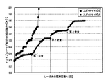
図1に回路図で示すバラクタダイオード1を内蔵したピル型のガンダイオードに、図1に回路図で示すようにバイアス供給回路を接続して高周波発振器を構成した。まず、トリマブルチップ抵抗2として、その抵抗値の調整範囲として所望の周波数の可変範囲を得ることができる1〜10kΩ(この場合は初期値が1kΩであり、調整可能な最大値が10kΩである。)のものを選定し、複数のトリマブルチップ抵抗2について図3(a)に示すようなトリミングを行なって、その抵抗値の制御性について確認した。図13にその一例を線図で示す。
A high frequency oscillator is configured by connecting a bias supply circuit to a pill type Gunn diode having a built-in
図13は、本発明の高周波発振器の実施例におけるトリマブルチップ抵抗2のトリミング処理回数とその抵抗値との関係を示す線図であり、横軸はトリミング処理回数としてのパルス状のレーザ光の照射回数N(単位:回)を、縦軸はトリマブルチップ抵抗2の電極2c1,2c2間の抵抗値Rt(単位:kΩ)を示しており、黒四角および黒丸の点はそれぞれ比較的スポットサイズの大きいレーザ光および比較的スポットサイズの小さいレーザ光を抵抗体層2bに照射したときのレーザ光の照射回数Nに対する抵抗値Rtの実測値を示している。
FIG. 13 is a diagram showing the relationship between the number of trimming processes of the
図13に示す結果から、トリマブルチップ抵抗2の抵抗値はレーザ光の照射回数Nにほぼ比例して増加し、その増加の割合は照射するレーザ光のスポットサイズにより異なっており、これらレーザ光のスポットサイズおよび照射回数Nによりトリマブルチップ抵抗2の抵抗値を適切に調整することができることがわかった。また、レーザ光を照射する際に、抵抗体層2bの同じ位置に複数回の照射を行なってから次の位置にレーザ光の照射点を走査するといった方法でレーザ光の照射を行なったが、比較的スポットサイズの小さいレーザ光を用いてトリミングを行なったときに顕著にわかる通り、同じ照射点での照射回数Nが増えるに従って抵抗値Rtが飽和する傾向にあることがわかり、この方法によれば所望の抵抗値に再現性よく確実にトリミングすることができることがわかった。また、このような走査を複数回繰り返すことにより抵抗値Rtが階段状に除々に増加していっており、この方法によれば緻密にトリミングすることができることがわかった。また、以上のことから、さらに緻密にトリミングするには、走査のピッチを少なくしたりレーザ光のスポットサイズをさらに小さくしたりして、階段状に増加する抵抗値Rtの増加の幅を狭くすればよいことが推察された。
From the results shown in FIG. 13, the resistance value of the
なお、この実施例では、一回の照射当たりにトリミングされる面積は、レーザ光のスポットサイズをレーザ光を透過させるスリットの幅を変えて一回の照射当たりの照射面積を変えることにより制御したが、レーザ光の強度や一回の照射当たりの照射時間により制御するようにしても構わない。 In this example, the area trimmed per one irradiation was controlled by changing the irradiation area per one irradiation by changing the width of the slit through which the laser beam spot size was transmitted. However, it may be controlled by the intensity of the laser beam or the irradiation time per irradiation.
次に、このトリマブルチップ抵抗2を用いて、レーザ光の強度を適宜変えながら上記のようなトリミングを複数回行なって、発振特性の中でも特性の変化が顕著である発振周波数の制御性について確認した。その一例を図14に線図で示す。
Next, using this
図14は、本発明の高周波発振器の実施例におけるトリマブルチップ抵抗2の抵抗値と発振周波数との関係を示す線図であり、横軸はトリマブルチップ抵抗2の抵抗値Rt(単位:kΩ)を、縦軸は高周波発振器の発振周波数ft(単位:GHz)を示しており、実線は抵抗値Rtの設定値に対する発振周波数ftの実測値を示している。なお、高周波発振器の負荷条件は一定とした。
FIG. 14 is a diagram showing the relationship between the resistance value of the
図14に示す結果から、抵抗値Rtの設定値を1〜10kΩ程度の範囲で変化させるとそれに比例して発振周波数が直線的に変化しており、この例では周波数を76.5GHzを中心に±0.2GHz程度変化させることができていることから、トリマブルチップ抵抗2により発振周波数ftを十分に調整することができることが確認できた。
From the results shown in FIG. 14, when the set value of the resistance value Rt is changed in the range of about 1 to 10 kΩ, the oscillation frequency changes linearly in proportion to this, and in this example, the frequency is ± 66.5 GHz. Since it can be changed by about 0.2 GHz, it was confirmed that the oscillation frequency ft can be sufficiently adjusted by the
次に、このような高周波発振器を用いて図4および図6に示す高周波送受信器を30台試作して、それぞれに上記のような方法で発振周波数fを調整してから、第3の誘電体線路25の端部に接続された送受信アンテナ15を取り外してその端部にスペクトラムアナライザの試験端子(テストポート)を接続して、その接続部から出力される周波数変調がかかった送信用高周波信号を30台全てについて測定したところ、30台とも周波数変調がかかった送信用高周波信号の発振周波数(周波数変調の中心周波数)および周波数変調幅が均一であり、良好な発振特性を有していることが確認された。なお、この実施例においては、バラクタダイオードの特性が比較的均一であったため、周波数変調幅を調整する必要はなかった。
Next, 30 high-frequency transceivers shown in FIGS. 4 and 6 were prototyped using such a high-frequency oscillator, and after adjusting the oscillation frequency f by the above method, the third dielectric Remove the transmit / receive
そして、最後に、この高周波送受信器を備えたレーダ装置を構成し、レーダ装置に近づいてくる探知対象物を探知するレーダ探知テストを行なったところ、高周波発振器が適切に動作するように上記のようなチューニングをしたレーダ装置は、速く確実に安定して距離情報を出力することを確認した。 Finally, when the radar apparatus including the high-frequency transmitter / receiver is configured and a radar detection test for detecting a detection object approaching the radar apparatus is performed, the high-frequency oscillator is operated as described above. It was confirmed that the radar device that was tuned properly outputs distance information quickly and reliably.
かくして、本発明によれば、高周波発振器の構成要素である可変容量素子のバイアス供給回路が、半固定抵抗器を具備しており、この半固定抵抗器により発振周波数や周波数変調幅等の発振特性を所望の状態にチューニングすることができ、良好な発振特性を安定して得ることができる高周波発振器となった。また、それを用いた高周波送受信器は高性能なものとなった。 Thus, according to the present invention, the bias supply circuit of the variable capacitance element, which is a component of the high-frequency oscillator, includes a semi-fixed resistor, and oscillation characteristics such as an oscillation frequency and a frequency modulation width are provided by the semi-fixed resistor. Can be tuned to a desired state, and a high-frequency oscillator can be obtained which can stably obtain good oscillation characteristics. Moreover, the high frequency transmitter / receiver using it became a high performance thing.
なお、本発明は以上の実施の形態の例および実施例に限定されるものではなく、本発明の要旨を逸脱しない範囲内で種々の変更を施すことは何等差し支えない。例えば、ガンダイオード52のバイアス供給回路53を、ガンダイオード52に印加するバイアス電圧を調節する半固定抵抗器を具備するものとしてもよい。この場合には、発振出力や負荷特性をも調整することができる高周波発振器となる。また、半固定抵抗器として、複数の固定抵抗が接続された固定抵抗ネットワークの接点をリレーで切り替えるようにしたものを用いてもよい。この場合には、固定抵抗ネットワークの抵抗値を動的に設定することができ、例えば、環境条件の変化に応じて高周波発振器11の動作が適切になるように動的に高周波発振器11のバイアス電圧を変更したり、変調器13の動作に同期させて高周波発振器11のバイアス電圧を変更したりするといったようなことができるものとなる。
Note that the present invention is not limited to the above-described embodiments and examples, and various modifications may be made without departing from the scope of the present invention. For example, the
1:バラクタダイオード
2:トリマブルチップ抵抗
2a:誘電体基体
2b:抵抗体層
2c1:電極
2c2:電極
2d:トリミング部
2d1,2d3:第1カット
2d2,2d4:第2カット
3:チョークインダクタ
4:変調信号源
5:試験用端子
11:高周波発振器
12:分岐器
12a:入力端
12b:一方の出力端
12c:他方の出力端
13:変調器
13a:入力端
13b:出力端
14:信号分離器としてのサーキュレータ
14a:第1の端子
14b:第2の端子
14c:第3の端子
15:送受信アンテナ
16:ミキサー
17:スイッチ
18:アイソレータ
18a:入力端子
18b:出力端子
19:送信アンテナ
20:受信アンテナ
21,31:平板導体
22,32:第1の誘電体線路
23,33:第2の誘電体線路
24,34:フェライト板
24a,34a:第1の端子
24b,34b:第2の端子
24c,34c:第3の端子
25,35:第3の誘電体線路
26,36:第4の誘電体線路
27,37:第5の誘電体線路
28,38a,38b:無反射終端器
39:第6の誘電体線路
40,44:基板
41:チョーク型バイアス供給線路
42:端子
43:高周波変調用素子
45:高周波検波用素子
51:導波管
52:ガンダイオード
53,56:バイアス供給回路
54:共振器
55:バラクタダイオード
51a:短絡端
51b:出力端
61,62:平板導体
63:誘電体線路
71:切替え器としての切替えRFスイッチ
71a:入力端
71b:一方の出力端
71c:他方の出力端
72:信号分離器としての第2の切替えRFスイッチ
72a:第2の端子
72b:第1の端子
72c:第3の端子
73:分岐器としてのラットレース型ハイブリッド結合器
73a:入力端
73b:一方の出力端
73c:他方の出力端
74:終端抵抗
75:信号分離器としての第2のラットレース型ハイブリッド結合器
75a:第1の端子
75b:第2の端子
75c:第3の端子
76:終端抵抗
1: Varactor diode 2: Trimmable chip resistor 2a: Dielectric substrate 2b: Resistor layer 2c1: Electrode 2c2:
11: High frequency oscillator
12: Turnout
12a: Input terminal
12b: One output terminal
12c: The other output terminal
13: Modulator
13a: Input terminal
13b: Output terminal
14: Circulator as signal separator
14a: First terminal
14b: Second terminal
14c: Third terminal
15: Transmit / receive antenna
16: Mixer
17: Switch
18: Isolator
18a: Input terminal
18b: Output terminal
19: Transmitting antenna
20: Receive antenna
21, 31: Flat conductor
22, 32: First dielectric line
23, 33: Second dielectric line
24, 34: Ferrite plate
24a, 34a: first terminal
24b, 34b: second terminal
24c, 34c: Third terminal
25, 35: Third dielectric line
26, 36: Fourth dielectric line
27, 37: Fifth dielectric line
28, 38a, 38b: Non-reflective terminator
39: Sixth dielectric line
40, 44: Board
41: Choke-type bias supply line
42: Terminal
43: High-frequency modulation element
45: High-frequency detection element
51: Waveguide
52: Gunn diode
53, 56: Bias supply circuit
54: Resonator
55: Varactor diode
51a: Short circuit end
51b: Output terminal
61, 62: Flat conductor
63: Dielectric line
71: Switching RF switch as a switch
71a: Input terminal
71b: One output terminal
71c: the other output terminal
72: Second switching RF switch as signal separator
72a: Second terminal
72b: first terminal
72c: Third terminal
73: Rat race type hybrid coupler as branching device
73a: Input terminal
73b: One output terminal
73c: The other output terminal
74: Termination resistor
75: Second rat race hybrid coupler as signal separator
75a: First terminal
75b: Second terminal
75c: Third terminal
76: Terminating resistor
Claims (12)
該高周波発振用素子に接続された共振器と、
該共振器に設けられた、共振周波数を変化させる可変容量素子と、
該可変容量素子に接続された、容量を変化させるために印加するバイアス電圧を供給するバイアス供給回路とを具備しており、
該バイアス供給回路は、前記バイアス電圧を調節する半固定抵抗器を具備することを特徴とする高周波発振器。 A high-frequency oscillation element for generating a high-frequency signal;
A resonator connected to the high-frequency oscillation element;
A variable capacitance element provided in the resonator for changing a resonance frequency;
A bias supply circuit connected to the variable capacitance element for supplying a bias voltage to be applied to change the capacitance;
The bias supply circuit includes a semi-fixed resistor for adjusting the bias voltage.
2つの出力端を有し、前記高周波発振器の出力端側に接続され、前記高周波信号を分岐して一方の出力端と他方の出力端とに出力する分岐器と、
前記一方の出力端に接続された、この一方の出力端に分岐された高周波信号を変調して送信用高周波信号を出力する変調器と、
第1の端子,第2の端子および第3の端子を有し、この順に一つの端子から入力された高周波信号を隣接する次の端子より出力するとともに、前記変調器の出力が前記第1の端子に入力される信号分離器と、
この信号分離器の前記第2の端子に接続された送受信アンテナと、
前記分岐器の前記他方の出力端と前記信号分離器の前記第3の端子との間に接続された、前記他方の出力端に分岐された高周波信号と前記送受信アンテナで受信した高周波信号とを混合して中間周波信号を出力するミキサーとを具備することを特徴とする高周波送受信器。 A high-frequency oscillator according to any one of claims 1 to 3,
A branching device having two output ends, connected to the output end side of the high-frequency oscillator, branching the high-frequency signal and outputting the branched signal to one output end and the other output end;
A modulator connected to the one output end and modulating a high-frequency signal branched to the one output end to output a transmission high-frequency signal;
A first terminal, a second terminal, and a third terminal; a high-frequency signal input from one terminal in this order is output from an adjacent next terminal; and an output of the modulator is the first terminal A signal separator input to the terminal;
A transmitting and receiving antenna connected to the second terminal of the signal separator;
A high-frequency signal branched to the other output end connected between the other output end of the branching device and the third terminal of the signal separator and a high-frequency signal received by the transmitting / receiving antenna A high-frequency transmitter / receiver comprising a mixer that mixes and outputs an intermediate frequency signal.
2つの出力端を有し、前記高周波発振器の出力端側に接続され、前記高周波信号を分岐して一方の出力端と他方の出力端とに出力する分岐器と、
前記一方の出力端に接続された、この一方の出力端に分岐された高周波信号を変調して送信用高周波信号を出力する変調器と、
入力端子と出力端子とを有し、前記変調器の出力端に前記入力端子が接続され、前記入力端子側から前記出力端子側へ前記送信用高周波信号を透過させるアイソレータと、
このアイソレータの前記出力端子に接続された送信アンテナと、
前記分岐器の前記他方の出力端側に接続された受信アンテナと、
前記分岐器の前記他方の出力端と前記受信アンテナとの間に接続された、前記他方の出力端に分岐された高周波信号と前記受信アンテナで受信した高周波信号とを混合して中間周波信号を出力するミキサーとを具備することを特徴とする高周波送受信器。 A high-frequency oscillator according to any one of claims 1 to 3,
A branching device having two output ends, connected to the output end side of the high-frequency oscillator, branching the high-frequency signal and outputting the branched signal to one output end and the other output end;
A modulator connected to the one output end and modulating a high-frequency signal branched to the one output end to output a transmission high-frequency signal;
An isolator having an input terminal and an output terminal, the input terminal being connected to an output end of the modulator, and transmitting the high-frequency signal for transmission from the input terminal side to the output terminal side;
A transmitting antenna connected to the output terminal of the isolator;
A receiving antenna connected to the other output end of the splitter;
The intermediate frequency signal is obtained by mixing the high-frequency signal branched between the other output end and the high-frequency signal received by the receiving antenna, connected between the other output end of the branching device and the receiving antenna. A high-frequency transmitter / receiver comprising a mixer for output.
2つの出力端を有し、前記高周波発振器の出力端側に接続され、前記高周波信号を一方の出力端および他方の出力端から選択的に出力する切替え器と、
第1の端子,第2の端子および第3の端子を有し、この順に一つの端子から入力された高周波信号を隣接する次の端子より出力するとともに、前記一方の出力端から出力される高周波信号が前記第1の端子に入力される信号分離器と、
前記第2の端子に接続された送受信アンテナと、
前記他方の出力端と前記第3の端子とに接続され、前記他方の出力端から出力される高周波信号と前記アンテナで受信した高周波信号とを混合して中間周波信号を出力するミキサーとを含むことを特徴とする高周波送受信器。 A high-frequency oscillator according to any one of claims 1 to 3,
A switch that has two output ends, is connected to the output end side of the high-frequency oscillator, and selectively outputs the high-frequency signal from one output end and the other output end;
A first terminal, a second terminal, and a third terminal are provided. A high-frequency signal input from one terminal in this order is output from an adjacent next terminal, and a high-frequency signal output from the one output terminal. A signal separator in which a signal is input to the first terminal;
A transmitting and receiving antenna connected to the second terminal;
A mixer that is connected to the other output end and the third terminal and that mixes a high-frequency signal output from the other output end and a high-frequency signal received by the antenna to output an intermediate frequency signal; A high frequency transceiver characterized by that.
2つの出力端を有し、前記高周波発振器の出力端側に接続され、前記高周波信号を一方の出力端および他方の出力端から選択的に出力する切替え器と、
前記一方の出力端に接続された送信アンテナと、
受信アンテナと、
前記他方の出力端と前記受信アンテナとに接続され、前記他方の出力端から出力される高周波信号と前記受信アンテナで受信した高周波信号とを混合して中間周波信号を出力するミキサーとを含むことを特徴とする高周波送受信器。 A high-frequency oscillator according to any one of claims 1 to 3,
A switch that has two output ends, is connected to the output end side of the high-frequency oscillator, and selectively outputs the high-frequency signal from one output end and the other output end;
A transmitting antenna connected to the one output end;
A receiving antenna;
A mixer that is connected to the other output end and the receiving antenna, and that mixes a high-frequency signal output from the other output end and a high-frequency signal received by the receiving antenna to output an intermediate frequency signal; A high frequency transceiver characterized by.
2つの出力端を有し、前記高周波発振器の出力端側に接続され、前記高周波信号を分岐して一方の出力端と他方の出力端とに出力する分岐器と、
第1の端子,第2の端子および第3の端子を有し、この順に一つの端子から入力された高周波信号を隣接する次の端子より出力するとともに、前記分岐器の前記一方の出力端からの出力が前記第1の端子に入力される信号分離器と、
この信号分離器の前記第2の端子に接続された送受信アンテナと、
前記分岐器の前記他方の出力端と前記信号分離器の前記第3の端子との間に接続され、前記他方の出力端に分岐された高周波信号と前記送受信アンテナで受信した高周波信号とを混合して中間周波信号を出力するミキサーとを具備することを特徴とする高周波送受信器。 A high-frequency oscillator according to any one of claims 1 to 3,
A branching device having two output ends, connected to the output end side of the high-frequency oscillator, branching the high-frequency signal and outputting the branched signal to one output end and the other output end;
A first terminal, a second terminal, and a third terminal are provided, and a high-frequency signal input from one terminal in this order is output from the next adjacent terminal, and from the one output terminal of the branching device A signal separator that is input to the first terminal;
A transmitting and receiving antenna connected to the second terminal of the signal separator;
A high-frequency signal that is connected between the other output end of the branching device and the third terminal of the signal separator and that is branched to the other output end and a high-frequency signal received by the transmitting / receiving antenna are mixed. And a mixer for outputting an intermediate frequency signal.
2つの出力端を有し、前記高周波発振器の出力端側に接続され、前記高周波信号を分岐して一方の出力端と他方の出力端とに出力する分岐器と、
前記分岐器の前記一方の出力端に接続された送信アンテナと、
前記分岐器の前記他方の出力端側に接続された受信アンテナと、
前記分岐器の前記他方の出力端と前記受信アンテナとの間に接続された、前記他方の出力端に分岐された高周波信号と前記受信アンテナで受信した高周波信号とを混合して中間周波信号を出力するミキサーとを具備することを特徴とする高周波送受信器。 A high-frequency oscillator according to any one of claims 1 to 3,
A branching device having two output ends, connected to the output end side of the high-frequency oscillator, branching the high-frequency signal and outputting the branched signal to one output end and the other output end;
A transmission antenna connected to the one output terminal of the branching device;
A receiving antenna connected to the other output end of the splitter;
The intermediate frequency signal is obtained by mixing the high-frequency signal branched between the other output end and the high-frequency signal received by the receiving antenna, connected between the other output end of the branching device and the receiving antenna. A high-frequency transmitter / receiver comprising a mixer for output.
Priority Applications (1)
| Application Number | Priority Date | Filing Date | Title |
|---|---|---|---|
| JP2005188644A JP2006050580A (en) | 2004-06-29 | 2005-06-28 | High-frequency oscillator,high-frequency send-receive apparatus and radar apparatus using it, radar apparatus mounting vehicle, and radar apparatus mounting small ship |
Applications Claiming Priority (2)
| Application Number | Priority Date | Filing Date | Title |
|---|---|---|---|
| JP2004191732 | 2004-06-29 | ||
| JP2005188644A JP2006050580A (en) | 2004-06-29 | 2005-06-28 | High-frequency oscillator,high-frequency send-receive apparatus and radar apparatus using it, radar apparatus mounting vehicle, and radar apparatus mounting small ship |
Publications (2)
| Publication Number | Publication Date |
|---|---|
| JP2006050580A true JP2006050580A (en) | 2006-02-16 |
| JP2006050580A5 JP2006050580A5 (en) | 2007-11-01 |
Family
ID=36028540
Family Applications (1)
| Application Number | Title | Priority Date | Filing Date |
|---|---|---|---|
| JP2005188644A Pending JP2006050580A (en) | 2004-06-29 | 2005-06-28 | High-frequency oscillator,high-frequency send-receive apparatus and radar apparatus using it, radar apparatus mounting vehicle, and radar apparatus mounting small ship |
Country Status (1)
| Country | Link |
|---|---|
| JP (1) | JP2006050580A (en) |
Cited By (5)
| Publication number | Priority date | Publication date | Assignee | Title |
|---|---|---|---|---|
| US7265711B2 (en) * | 2004-06-29 | 2007-09-04 | Kyocera Corporation | High-frequency oscillator, high-frequency transmission-reception apparatus using the same, radar apparatus, and radar-apparatus-equipped vehicle and small boat equipped with the same |
| JP2008035187A (en) * | 2006-07-28 | 2008-02-14 | Kyocera Corp | Directional coupler, high frequency transmitter-receiver using it, radar apparatus, vehicle loaded with radar apparatus, and small-sized ship loaded with radar apparatus |
| JP2013167524A (en) * | 2012-02-15 | 2013-08-29 | Nippon Telegr & Teleph Corp <Ntt> | Electromagnetic wave imaging device and electromagnetic wave imaging method |
| JP2017198474A (en) * | 2016-04-25 | 2017-11-02 | 株式会社ヨコオ | Pulse radar device and component of the same |
| JP2020020876A (en) * | 2018-07-30 | 2020-02-06 | 住友大阪セメント株式会社 | Optical modulator and optical transmission device |
Citations (9)
| Publication number | Priority date | Publication date | Assignee | Title |
|---|---|---|---|---|
| JPS6154704A (en) * | 1984-08-24 | 1986-03-19 | Tokyo Keiki Co Ltd | Microwave oscillator |
| JPH0540169A (en) * | 1991-08-08 | 1993-02-19 | Fujitsu Ltd | Fm-cw radar device |
| JPH08340214A (en) * | 1995-06-14 | 1996-12-24 | Meidensha Corp | Crystal oscillator circuit |
| JPH11298245A (en) * | 1998-04-16 | 1999-10-29 | Hokuriku Electric Ind Co Ltd | Temperature compensated crystal oscillator |
| JPH11352219A (en) * | 1998-06-05 | 1999-12-24 | Mitsubishi Electric Corp | Vehicle-mounted radar system |
| JP2000338233A (en) * | 1999-05-28 | 2000-12-08 | Mitsubishi Electric Corp | Pulse doppler radar device |
| JP2001264426A (en) * | 2000-03-17 | 2001-09-26 | Mitsubishi Electric Corp | Fm pulse doppler radar |
| JP2003198421A (en) * | 2001-12-25 | 2003-07-11 | Kyocera Corp | Millimeter wave receiver |
| JP2004120728A (en) * | 2002-09-25 | 2004-04-15 | Renesas Technology Corp | Oscillation circuit and semiconductor integrated circuit for communication |
-
2005
- 2005-06-28 JP JP2005188644A patent/JP2006050580A/en active Pending
Patent Citations (9)
| Publication number | Priority date | Publication date | Assignee | Title |
|---|---|---|---|---|
| JPS6154704A (en) * | 1984-08-24 | 1986-03-19 | Tokyo Keiki Co Ltd | Microwave oscillator |
| JPH0540169A (en) * | 1991-08-08 | 1993-02-19 | Fujitsu Ltd | Fm-cw radar device |
| JPH08340214A (en) * | 1995-06-14 | 1996-12-24 | Meidensha Corp | Crystal oscillator circuit |
| JPH11298245A (en) * | 1998-04-16 | 1999-10-29 | Hokuriku Electric Ind Co Ltd | Temperature compensated crystal oscillator |
| JPH11352219A (en) * | 1998-06-05 | 1999-12-24 | Mitsubishi Electric Corp | Vehicle-mounted radar system |
| JP2000338233A (en) * | 1999-05-28 | 2000-12-08 | Mitsubishi Electric Corp | Pulse doppler radar device |
| JP2001264426A (en) * | 2000-03-17 | 2001-09-26 | Mitsubishi Electric Corp | Fm pulse doppler radar |
| JP2003198421A (en) * | 2001-12-25 | 2003-07-11 | Kyocera Corp | Millimeter wave receiver |
| JP2004120728A (en) * | 2002-09-25 | 2004-04-15 | Renesas Technology Corp | Oscillation circuit and semiconductor integrated circuit for communication |
Cited By (8)
| Publication number | Priority date | Publication date | Assignee | Title |
|---|---|---|---|---|
| US7265711B2 (en) * | 2004-06-29 | 2007-09-04 | Kyocera Corporation | High-frequency oscillator, high-frequency transmission-reception apparatus using the same, radar apparatus, and radar-apparatus-equipped vehicle and small boat equipped with the same |
| JP2008035187A (en) * | 2006-07-28 | 2008-02-14 | Kyocera Corp | Directional coupler, high frequency transmitter-receiver using it, radar apparatus, vehicle loaded with radar apparatus, and small-sized ship loaded with radar apparatus |
| JP4624319B2 (en) * | 2006-07-28 | 2011-02-02 | 京セラ株式会社 | Manufacturing method of directional coupler, high-frequency transceiver and radar device using the same, vehicle mounted with radar device, and small ship equipped with radar device |
| JP2013167524A (en) * | 2012-02-15 | 2013-08-29 | Nippon Telegr & Teleph Corp <Ntt> | Electromagnetic wave imaging device and electromagnetic wave imaging method |
| JP2017198474A (en) * | 2016-04-25 | 2017-11-02 | 株式会社ヨコオ | Pulse radar device and component of the same |
| JP2020020876A (en) * | 2018-07-30 | 2020-02-06 | 住友大阪セメント株式会社 | Optical modulator and optical transmission device |
| JP7187871B2 (en) | 2018-07-30 | 2022-12-13 | 住友大阪セメント株式会社 | Optical modulator and optical transmitter |
| JP7187871B6 (en) | 2018-07-30 | 2023-01-05 | 住友大阪セメント株式会社 | Optical modulator and optical transmitter |
Similar Documents
| Publication | Publication Date | Title |
|---|---|---|
| US20060017607A1 (en) | Amplitude modulator, selector switch, high frequency transmitting/receiving apparatus including the same, and radar apparatus, and radar apparatus-mounting vehicle and radar apparatus-mounting small ship | |
| US7265711B2 (en) | High-frequency oscillator, high-frequency transmission-reception apparatus using the same, radar apparatus, and radar-apparatus-equipped vehicle and small boat equipped with the same | |
| JP4446785B2 (en) | High-frequency transceiver, radar device including the same, radar device-equipped vehicle equipped with the same, and radar device-equipped small vessel | |
| US20060214842A1 (en) | Mixer, High-Frequency transmitting/receiving apparatus having the same, radarapparatus having the high-frequency transmitting/receiving apparatus, and vehicle equipped with radar apparatus | |
| EP0513287A1 (en) | Motion detector unit. | |
| JP2006050580A (en) | High-frequency oscillator,high-frequency send-receive apparatus and radar apparatus using it, radar apparatus mounting vehicle, and radar apparatus mounting small ship | |
| JP4624195B2 (en) | High frequency transceiver and radar device | |
| JP4498065B2 (en) | Directional coupler type branching device, high-frequency transmitter / receiver including the same, and radar apparatus | |
| JP4446939B2 (en) | Amplitude modulator, changeover switch, high-frequency transmitter / receiver including the same, and radar apparatus | |
| JP4712083B2 (en) | High frequency transceiver and radar device | |
| JP4707731B2 (en) | Isolator, high-frequency oscillator, high-frequency transmitter / receiver, and radar apparatus using the same | |
| JP4206358B2 (en) | Isolator, high-frequency oscillator, high-frequency transmitter / receiver, and radar apparatus using the same | |
| JP4883922B2 (en) | High frequency transmitter / receiver and radar apparatus including the same | |
| JP4377739B2 (en) | High frequency transmitter / receiver, radar apparatus including the same, vehicle mounted with radar apparatus, and small ship mounted with radar apparatus | |
| JP4416562B2 (en) | MODULATOR, AMPLITUDE MODULATOR, HIGH FREQUENCY TRANSMITTER / RECEIVER USING THE SAME, RADAR DEVICE, RADAR DEVICE MOUNTED VEHICLE, AND RADAR DEVICE MOUNTED SHIP | |
| JP4446798B2 (en) | High-frequency transceiver, radar device including the same, radar device-equipped vehicle equipped with the same, and radar device-equipped small vessel | |
| JP2006157289A (en) | Attenuator and high frequency transmitter-receiver using same, radar apparatus, vehicle with radar apparatus mounted thereon, and small craft with radar apparatus mounted therein | |
| JP2005274331A (en) | High frequency transceiver, radar system provided therewith, vehicle mounted with radar system, and small vessel mounted with radar system | |
| JP4423151B2 (en) | High frequency transmitter / receiver and radar apparatus including the same | |
| JP2006041789A (en) | Non-radiative dielectric line, high frequency transmitter-receiver and radar employing the same, radar mounted vehicle and radar mounted small ship | |
| JP4268507B2 (en) | Amplitude modulator for non-radiative dielectric lines and millimeter wave transceiver using the same | |
| JP2006128929A (en) | Attenuator and high frequency transmitter-receiver using the same, radar apparatus, radar apparatus mounter vehicle, and radar apparatus mounter small ship | |
| JP2006064401A (en) | Modulator, high-frequency transmitter/receiver using it, radar apparatus, vehicle equipped with radar apparatus, and small vessel equipped with radar apparatus | |
| JP2006014202A (en) | Nonradioactive dielectric line, and high-frequency transmitter/receiver, radar device, radar device mounting vehicle, and radar device mounting small-sized ship using same | |
| JP2006128928A (en) | Attenuator and high frequency transmitter-receiver using the same, radar apparatus, radar apparatus mounter vehicle, and radar apparatus mounter small ship |
Legal Events
| Date | Code | Title | Description |
|---|---|---|---|
| A521 | Written amendment |
Free format text: JAPANESE INTERMEDIATE CODE: A523 Effective date: 20070913 |
|
| A621 | Written request for application examination |
Free format text: JAPANESE INTERMEDIATE CODE: A621 Effective date: 20080118 |
|
| A131 | Notification of reasons for refusal |
Free format text: JAPANESE INTERMEDIATE CODE: A131 Effective date: 20100525 |
|
| A521 | Written amendment |
Free format text: JAPANESE INTERMEDIATE CODE: A523 Effective date: 20100723 |
|
| A131 | Notification of reasons for refusal |
Free format text: JAPANESE INTERMEDIATE CODE: A131 Effective date: 20101026 |
|
| A521 | Written amendment |
Free format text: JAPANESE INTERMEDIATE CODE: A523 Effective date: 20101215 |
|
| A02 | Decision of refusal |
Free format text: JAPANESE INTERMEDIATE CODE: A02 Effective date: 20110224 |