JP2006024703A - Nitride semiconductor laser device - Google Patents
Nitride semiconductor laser device Download PDFInfo
- Publication number
- JP2006024703A JP2006024703A JP2004200887A JP2004200887A JP2006024703A JP 2006024703 A JP2006024703 A JP 2006024703A JP 2004200887 A JP2004200887 A JP 2004200887A JP 2004200887 A JP2004200887 A JP 2004200887A JP 2006024703 A JP2006024703 A JP 2006024703A
- Authority
- JP
- Japan
- Prior art keywords
- layer
- film
- nitride semiconductor
- semiconductor layer
- electrode
- Prior art date
- Legal status (The legal status is an assumption and is not a legal conclusion. Google has not performed a legal analysis and makes no representation as to the accuracy of the status listed.)
- Pending
Links
Images

Abstract
Description
今日、窒化物半導体を用いた半導体レーザは、紫外域から赤色に至るまで、幅広い波長域での発振が可能と考えられ、その応用範囲は、DVDなど、大容量・高密度の情報記録・再生録画が可能な光ディスクシステムへの利用にとどまらず、レーザプリンタ、光ネットワークなどの光源等として期待されている。
窒化物半導体レーザ素子は、例えば、基板上に、n型窒化物半導体層、活性層、p型窒化物半導体層がこの順に積層され、n型及びp型窒化物半導体層に、それぞれ電極が形成されて構成されている。
Today, semiconductor lasers using nitride semiconductors are considered capable of oscillating in a wide wavelength range from the ultraviolet to the red, and their application range is large-capacity and high-density information recording / reproduction such as DVD. It is expected not only for use in an optical disc system capable of recording, but also as a light source for laser printers, optical networks, and the like.
In a nitride semiconductor laser element, for example, an n-type nitride semiconductor layer, an active layer, and a p-type nitride semiconductor layer are stacked in this order on a substrate, and electrodes are formed on the n-type and p-type nitride semiconductor layers, respectively. Has been configured.
また、このような積層構造のレーザ素子では、p型窒化物半導体層表面にストライプ状のリッジが形成されており、さらに、リッジの両側のp型窒化物半導体層の露出面に、埋め込み膜が形成されている。これによって実効屈折率型の導波路構造とすることができる。
このように、リッジを形成することにより、さらにその両側に埋め込み膜を形成することにより、リッジ直下の導波路領域と、このリッジ両側直下の領域とにおける実効的な屈折率分布を確保し、光の閉じ込めを最適化し、横モードの制御を行うとともに、閾値の制御をも行っている。
また、ストライプ状の導波路構造を有するものとしては、上記のようなリッジを設けずに、平坦なp型窒化物半導体層表面にストライプ状の電極を設けたり、あるいはストライプ状の開口部を有する絶縁膜(埋込膜)を形成してその上に電極を設けることとで、電流注入領域をストライプ状に制御するもの、さらには半導体層中に電流狭窄層を設けるもの等があげられる。これらは表面にリッジを設けていないことでチップ化時の歩留まり等が優れており、また、リッジ形成工程がないので工程数も少ない等のメリットがある。
Further, in the laser element having such a laminated structure, a striped ridge is formed on the surface of the p-type nitride semiconductor layer, and a buried film is formed on the exposed surface of the p-type nitride semiconductor layer on both sides of the ridge. Is formed. Thus, an effective refractive index type waveguide structure can be obtained.
In this way, by forming a ridge and further forming a buried film on both sides of the ridge, an effective refractive index distribution is ensured in the waveguide region directly below the ridge and the region immediately below both sides of the ridge. The confinement is optimized, the transverse mode is controlled, and the threshold is also controlled.
In addition, the one having a striped waveguide structure is provided with a striped electrode on the flat p-type nitride semiconductor layer surface or having a striped opening without providing the ridge as described above. By forming an insulating film (embedded film) and providing an electrode on the insulating film (embedded film), the current injection region is controlled in a stripe shape, and further, the current confining layer is provided in the semiconductor layer. These have no ridges on the surface, so that the yield at the time of chip formation is excellent, and there is no ridge formation step, and there are advantages such as a small number of steps.
なお、埋め込み膜としては、TiO2、ZrO2、HfO2、CeO2、In2O3、Nd2O3、Sb2O3、SnO2、Ta2O5、ZnO等の誘電体膜が用いられている(例えば、特許文献1)。
特許文献1に示すような誘電体膜は、通常、各物質に固有の屈折率を有している。そのため、埋め込み膜として所望の屈折率を得るために、適切な材料を組み合わせて用いることなどが行われている。しかし、屈折率を満足させる材料を選択したとしても、その成膜方法や物理的な性質により、レーザ素子の埋め込み膜として十分に機能させることができないことがある。 A dielectric film as shown in Patent Document 1 usually has a refractive index specific to each substance. For this reason, in order to obtain a desired refractive index as a buried film, an appropriate material is used in combination. However, even if a material that satisfies the refractive index is selected, the material may not function sufficiently as a buried film of the laser element due to its film formation method and physical properties.
つまり、上述した誘電体膜は、通常スパッタ法等で形成され、ターゲット表面で酸素と反応させながら酸化物として成膜される。しかし、ターゲット面内に酸素と反応しやすい部分と反応しにくい部分が存在するため、成膜された埋め込み膜においては、面内方向又は膜厚方向で、均一な酸化物が形成されない場合がある。これにより、埋め込み膜として適当な屈折率を得ることができず、光閉じ込め等の制御ができなくなる。 That is, the above-described dielectric film is usually formed by sputtering or the like, and is formed as an oxide while reacting with oxygen on the target surface. However, there are portions in the target plane that are likely to react with oxygen and portions that are difficult to react, so in the formed buried film, a uniform oxide may not be formed in the in-plane direction or in the film thickness direction. . As a result, an appropriate refractive index cannot be obtained as a buried film, and light confinement or the like cannot be controlled.
また、レーザ素子にリッジが形成されている場合のみならず、リッジが形成されていない場合、すなわち、絶縁膜(埋込膜)にストライプ状の開口部を設けて半導体層から埋込膜上に渡って電極を形成する場合においても、材料によっては、その上に形成されるp電極との密着性が悪く、電極の剥がれを生じさせ、製品の歩留まりが低下するという問題もある。 Further, not only when the ridge is formed in the laser element but also when the ridge is not formed, that is, by providing a stripe-shaped opening in the insulating film (embedded film) from the semiconductor layer to the buried film. Even in the case of forming electrodes across the substrate, depending on the material, there is a problem in that the adhesion with the p-electrode formed thereon is poor, the electrodes are peeled off, and the product yield is lowered.
本発明は上記課題に鑑みなされたものであり、埋め込み膜としての屈折率を満足させながら、面内及び膜厚方向において所望の機能を有する膜を得ることができるとともに、p電極との剥がれを防止して、高品質の窒化物半導体レーザ素子を得ることを目的とする。 The present invention has been made in view of the above problems, and while satisfying the refractive index as a buried film, it is possible to obtain a film having a desired function in the plane and in the film thickness direction, and to remove the p electrode. An object is to obtain a high-quality nitride semiconductor laser device.
本発明の窒化物半導体レーザ素子は、第1窒化物半導体層、活性層及び第2窒化物半導体層がこの順に積層され、該第2窒化物半導体層上に埋め込み膜を介して電極が形成されて構成される窒化物半導体レーザ素子であって、前記埋め込み膜が、前記第2窒化物半導体層側から表面側にかけて(1)屈折率が、(2)酸素比率が及び/又は(3)密度が変化してなることを特徴とする。あるいは、埋め込み膜が、少なくとも2層で形成され、前記第2窒化物半導体層側の層と表面側の層との表面粗さが異なることを特徴とする。 In the nitride semiconductor laser device of the present invention, a first nitride semiconductor layer, an active layer, and a second nitride semiconductor layer are stacked in this order, and an electrode is formed on the second nitride semiconductor layer via a buried film. In the nitride semiconductor laser device configured as described above, the embedded film has (1) a refractive index, (2) an oxygen ratio and / or (3) density from the second nitride semiconductor layer side to the surface side. Is characterized by changing. Alternatively, the buried film is formed of at least two layers, and the surface roughness is different between the layer on the second nitride semiconductor layer side and the layer on the surface side.
上記窒化物半導体レーザ素子においては、埋め込み膜の屈折率が第2窒化物半導体層側に対して表面側が大きいか、埋め込み膜の酸素比率が第2窒化物半導体層側に対して表面側が小さいか、埋め込み膜の密度が第2窒化物半導体層側に対して表面側が大きいか、及び/又は、(埋め込み膜が2層以上の積層膜の場合)埋め込み膜の最表面側の層の表面が、埋め込み層の中で最も平坦、言い換えると、表面粗さが小さいことが好ましい。 In the nitride semiconductor laser device, whether the refractive index of the buried film is larger on the surface side than the second nitride semiconductor layer side, or is the oxygen ratio of the buried film smaller on the surface side than the second nitride semiconductor layer side? The density of the buried film is larger on the surface side than the second nitride semiconductor layer side, and / or the surface of the outermost layer side of the buried film (when the buried film is a laminated film of two or more layers) It is preferable that the buried layer is the flattest, in other words, the surface roughness is small.
特に、第2窒化物半導体層側の埋め込み膜の屈折率が2.20以下、表面側の埋め込み膜の屈折率が2.20より大きいことがより好ましい。
また、埋め込み膜は、単層で構成されていてもよいし、2層以上の積層構造の膜で構成されていてもよい。
さらに、埋め込み膜は、少なくとも第2窒化物半導体層側において酸素を含むか、酸化物から構成されており、特に、酸素とジルコニウムとからなることが好ましい。
また、上記窒化物半導体レーザ素子においては、第2窒化物半導体層の表面にリッジが形成されていることが好ましい。
In particular, the refractive index of the buried film on the second nitride semiconductor layer side is more preferably 2.20 or less, and the refractive index of the buried film on the surface side is more preferably 2.20.
The embedded film may be composed of a single layer or a film having a laminated structure of two or more layers.
Further, the buried film contains oxygen or is composed of an oxide at least on the second nitride semiconductor layer side, and is preferably composed of oxygen and zirconium.
In the nitride semiconductor laser element, it is preferable that a ridge is formed on the surface of the second nitride semiconductor layer.
本発明の窒化物半導体レーザ素子によれば、屈折率、酸素比率、密度又は表面粗さが膜厚方向において変化することにより、埋め込み膜の表面側、つまり、電極と接触する側において、非常に質の良好な膜を配置することができるために、電極との密着性をより強固にすることができる。これにより、電極の剥がれを防止することができ、歩留まりのよい製品を、高品質で提供することが可能となる。
また、埋め込み膜が2層以上の積層構造で形成される場合には、所望の屈折率を得るなど、所望の膜質を確保しながら、埋め込み膜自体の膜厚を制御することが可能となり、窒化物半導体レーザ素子の設計が容易となる。
特に、埋め込み膜が、酸素及びジルコニウムという同じ構成元素で形成されている場合には、異なる材料が接触する界面がないために、積層膜内部における密着性が良好となり、屈折率及び電極との密着性の双方を満足させることができる。
According to the nitride semiconductor laser device of the present invention, the refractive index, oxygen ratio, density, or surface roughness changes in the film thickness direction, so that the surface side of the buried film, that is, the side in contact with the electrode is very Since a film having a good quality can be disposed, the adhesion with the electrode can be further strengthened. As a result, peeling of the electrodes can be prevented, and a product with a high yield can be provided with high quality.
Further, when the buried film is formed in a laminated structure of two or more layers, it becomes possible to control the film thickness of the buried film itself while ensuring a desired film quality, such as obtaining a desired refractive index. It becomes easy to design a semiconductor laser device.
In particular, when the buried film is formed of the same constituent elements such as oxygen and zirconium, there is no interface between different materials, so the adhesion within the laminated film is good, and the refractive index and adhesion to the electrode are good. Both sexes can be satisfied.
本発明の窒化物半導体レーザ素子は、典型的には、第1窒化物半導体層、活性層及び第2窒化物半導体層がこの順に積層され、第2窒化物半導体層上に埋め込み膜を一部に介して電極が形成されて構成される窒化物半導体レーザ素子である。
ここで埋め込み膜としては、得ようとする特性に応じて適宜その材料を選択することができる。例えば、少なくとも酸素を含有する膜であってもよいし、Zr、Hf、Ce、In、Sb、Sn、Ta、Zn、Si、Al、Hf等の金属を含有する膜であってもよい。さらに、酸素とこれら金属とを含有する膜であってもよい。具体的には、これら金属等の酸化物膜が好適に用いられる。なかでも、膜厚方向において、構成元素が同じ又は同一のものを含み、その組成比などが異なるものであることが好ましい。例えば、酸素とジルコニウムとを有する膜(以下「酸化ジルコニウム」と称する)がその一部に含まれているものが好ましく、埋め込み膜全体が、酸素とジルコニウムとから構成されているものがより好ましい。
In the nitride semiconductor laser device of the present invention, typically, a first nitride semiconductor layer, an active layer, and a second nitride semiconductor layer are stacked in this order, and a part of the embedded film is formed on the second nitride semiconductor layer. The nitride semiconductor laser device is configured by forming an electrode through the electrode.
Here, the material for the buried film can be appropriately selected according to the characteristics to be obtained. For example, it may be a film containing at least oxygen, or a film containing a metal such as Zr, Hf, Ce, In, Sb, Sn, Ta, Zn, Si, Al, and Hf. Further, it may be a film containing oxygen and these metals. Specifically, oxide films of these metals are preferably used. Especially, it is preferable that the constituent elements include the same or the same constituent elements in the film thickness direction, and the composition ratios thereof are different. For example, a film containing oxygen and zirconium (hereinafter referred to as “zirconium oxide”) is preferably included in a part thereof, and the entire embedded film is more preferably composed of oxygen and zirconium.
本発明の埋め込み膜は、第2窒化物半導体層側から表面側(つまり電極側)にかけて、言い換えると膜厚方向において、(1)屈折率が、(2)酸素比率が、(3)密度が及び/又は(4)表面粗さが変化している膜である。なお、これらの1つのみが変化しているものであってもよいし、2つ以上が変化しているものであってもよいし、全てが変化しているものであってもよい。さらに、埋め込み膜を構成する材料において粒子の大きさが変化している膜であってもよい。 The buried film of the present invention has (1) the refractive index, (2) the oxygen ratio, and (3) the density from the second nitride semiconductor layer side to the surface side (that is, the electrode side), in other words, in the film thickness direction. And / or (4) a film with varying surface roughness. Only one of these may be changed, two or more may be changed, or all may be changed. Furthermore, a film in which the particle size of the material constituting the embedded film is changed may be used.
本発明において「第2窒化物半導体層側から表面側にかけて変化する」とは、徐々に変化してもよいし、段階的に変化してもよいし、大きくなるように変化してもよいし、小さくなるように変化してもよいし、大小がランダムに変化してもよい。また、徐々の変化であろうが、段階的な変化であろうが、いずれの場合においても、埋め込み膜自体は、単一の層で形成されていてもよいし、2層以上の膜が積層されて形成されていてもよい。なかでも、構成元素の異なる又は同じ2層以上の積層膜によって形成されることが好ましい。 In the present invention, “changes from the second nitride semiconductor layer side to the surface side” may change gradually, may change stepwise, or may change so as to increase. , It may change so as to become smaller, or may change randomly. Further, in any case, whether it is a gradual change or a gradual change, the embedded film itself may be formed of a single layer, or two or more layers are laminated. May be formed. Especially, it is preferable to form with the laminated film from which two or more layers differ in a structural element.
この変化によって、埋め込み膜としての機能を種々の機能を損なうことなく、十分に発揮させながら、電極との密着性を確保し、より向上させることを意図する。
例えば、最表面の膜(単層膜の最表面領域及び積層膜の最表面側の膜の双方を含む、以下同じ)は、その直下に位置する膜よりも大きい屈折率を有する膜が配置されてなる。言い換えると、最上層の直下には、最上層よりも小さい屈折率を有する膜が配置されていることが好ましい。例えば、最上層の膜の屈折率は、2.20よりも大きい、2.21以上、2.22以上、2.23以上の膜であることが適当である。また、第2窒化物半導体側の膜が2.20以下の屈折率であることが適当である。
By this change, it is intended to secure and improve the adhesion with the electrode while fully exerting the function as the buried film without impairing various functions.
For example, the outermost film (including both the outermost surface region of the single-layer film and the outermost film side of the laminated film, the same shall apply hereinafter) is provided with a film having a higher refractive index than the film located immediately below it. It becomes. In other words, it is preferable that a film having a refractive index smaller than that of the uppermost layer is disposed immediately below the uppermost layer. For example, the refractive index of the uppermost film is suitably a film of 2.21 or more, 2.22 or more, or 2.23 or more, which is larger than 2.20. Further, it is appropriate that the film on the second nitride semiconductor side has a refractive index of 2.20 or less.
なお、屈折率は、エリプソメトリーを利用した分光エリプソメータにより測定することができる。具体的には、J.A.WOOLLAM社製のHS−190等を用いることができる。
例えば、少なくとも2層の積層膜からなる場合は、少なくとも2層の膜の屈折率が異なることが適当である。下層膜が上層膜よりも屈折率が小さく設定されてなることが好ましく、さらに、下層膜の屈折率が2.20以下、2.15以下、2.10以下、2.05以下、2.00以下、上層膜の屈折率2.20より大きい、2.21以上、2.22以上、2.23以上であることがより好ましい。なお、この上下層膜の屈折率は、上下膜を積層させた状態で各膜の屈折率を別々に測定した値である。
The refractive index can be measured by a spectroscopic ellipsometer using ellipsometry. Specifically, J. et al. A. For example, HS-190 manufactured by WOOLLAM can be used.
For example, in the case where the laminated film is composed of at least two layers, it is appropriate that the refractive indexes of the at least two layers are different. The lower layer film is preferably set to have a refractive index smaller than that of the upper layer film. Further, the lower layer film has a refractive index of 2.20 or less, 2.15 or less, 2.10 or less, 2.05 or less, 2.00. Hereinafter, it is more preferable that the refractive index of the upper layer film is greater than 2.20, 2.21 or more, 2.22 or more, or 2.23 or more. The refractive index of the upper and lower layer films is a value obtained by separately measuring the refractive index of each film in a state where the upper and lower films are laminated.
あるいは、最表面の膜は、その直下に位置する膜と異なる酸素比率を有する膜が配置されてなる。
例えば、埋め込み膜が少なくとも2層の膜で形成されている場合には、少なくとも2層の膜の酸素の比率が異なることが適当であり、さらに、下層膜が上層膜よりも酸素の比率が大きく設定されてなることが好ましい。ここで酸素の比率が異なるとは、各膜における全元素数に対する酸素元素数の比が若干であっても異なることを意味する。各元素数は、オージェ電子分光法等を利用して測定することができる。
Alternatively, the outermost film is a film having an oxygen ratio different from that of the film located immediately below the outermost film.
For example, when the buried film is formed of at least two layers, it is appropriate that the oxygen ratio of the at least two layers is different, and the lower layer film has a larger oxygen ratio than the upper layer film. It is preferable to be set. Here, the ratio of oxygen is different means that the ratio of the number of oxygen elements to the total number of elements in each film is different even if it is slight. The number of each element can be measured using Auger electron spectroscopy or the like.
また、別の観点から、特に、埋め込み膜が2層以上の積層構造の場合、最表面の膜は、その直下に位置する膜と異なる表面粗さを有する膜が配置されてなる。
例えば、下層膜が上層膜(最表面側の層)よりも表面粗さが粗く設定されてなる、言い換えると、最表面側の層の表面が、埋め込み層の中で最も平坦であることが好ましい。なお、表面粗さは、分光エリプソメータを利用したラフネスとして、あるいは原子間力顕微鏡(AFM)等を利用して測定することができる。
From another point of view, in particular, when the buried film has a laminated structure of two or more layers, the film on the outermost surface is arranged with a film having a surface roughness different from that of the film located immediately below.
For example, the surface roughness of the lower layer film is set to be rougher than that of the upper layer film (the outermost layer), in other words, the surface of the outermost layer is preferably the flattest among the buried layers. . The surface roughness can be measured as roughness using a spectroscopic ellipsometer, or using an atomic force microscope (AFM) or the like.
さらに、別の観点から、最表面の膜は、その直下に位置する膜と異なる密度を有する膜が配置されてなる。
例えば、埋め込み膜が少なくとも2層の膜で形成されている場合には、密度が異なることが適当であり、下層膜が上層膜よりも密度が小さく形成されてなることが好ましい。
また、最表面の膜は、その直下に位置する膜と異なる結晶構造又は結晶粒の大きさを有する膜が配置されてなる。
Furthermore, from another point of view, the outermost film is a film having a density different from that of the film located immediately below the outermost film.
For example, when the buried film is formed of at least two layers, it is appropriate that the densities are different, and it is preferable that the lower layer film is formed to have a lower density than the upper layer film.
In addition, the outermost film is a film having a crystal structure or crystal grain size different from that of the film located immediately below.
例えば、埋め込み膜が少なくとも2層の膜で形成されている場合には、結晶構造又は結晶粒の大きさが異なることが適当であり、下層膜が上層膜よりも結晶粒が小さく形成されてなるか、緻密でない(粗である)結晶構造で形成されてなることが好ましい。
密度、結晶構造又は結晶粒の大きさは、例えば、断面を透過電子顕微鏡法(TEM)により観察する方法、走査型電子顕微鏡法(SEM)により観察する方法、電子回折パターン又はX線回折パターン等を測定する方法、超薄膜評価装置で観察する方法等によって測定することができる。
For example, when the buried film is formed of at least two layers, it is appropriate that the crystal structure or the crystal grain size is different, and the lower layer film is formed with smaller crystal grains than the upper layer film. Alternatively, it is preferably formed of a crystal structure that is not dense (rough).
The density, crystal structure, or crystal grain size is, for example, a method of observing a cross section by transmission electron microscopy (TEM), a method of observing by scanning electron microscopy (SEM), an electron diffraction pattern, an X-ray diffraction pattern, or the like It can measure by the method of measuring, the method of observing with an ultra-thin film evaluation apparatus, etc.
埋め込み膜は、当該分野で公知の方法によって形成することができる。例えば、蒸着法、スパッタ法、反応性スパッタ法、イオンビームアシスト蒸着法、イオンプレーティング法、レーザアブレーション法、CVD法、スプレー法、スピンコート法、ディップ法又はこれらの方法の2種以上を組み合わせる方法、あるいはこれらの方法と酸化処理(熱処理)とを組み合わせる方法等、種々の方法を利用することができる。また、埋め込み膜を単一層とする場合には、1つの成膜方法で、その成膜条件を異ならせるなどして、屈折率等を変化させることができる。 The buried film can be formed by a method known in the art. For example, vapor deposition method, sputtering method, reactive sputtering method, ion beam assisted vapor deposition method, ion plating method, laser ablation method, CVD method, spray method, spin coating method, dipping method or a combination of two or more of these methods Various methods such as a method or a combination of these methods and an oxidation treatment (heat treatment) can be used. In the case where the embedded film is a single layer, the refractive index and the like can be changed by changing the film forming conditions by one film forming method.
具体的には、埋め込み膜(例えば、酸化ジルコニウム)を成膜する際に、下層膜をスパッタ法で、上層膜を蒸着法で形成するなど、上下膜において異なる成膜方法を採用する方法が挙げられる。この際、まず、酸化ジルコニウムからなるターゲットを用いたスパッタ法で成膜し、その後、ジルコニウム膜を蒸着法により成膜し、その途中又は後に熱処理を行ってもよいし、ジルコニウム膜を各方法で形成した後に、熱処理を行って酸化ジルコニウム膜としてもよい。また、各方法での成膜時に徐々に又は急激に真空度を変えてもよいし(例えば、0.01〜2.0pa程度の範囲内で)、徐々に又は急激に基板温度を変えてもよいし(例えば、400〜1200℃程度の範囲内で)。 Specifically, when forming a buried film (for example, zirconium oxide), a method of adopting different film forming methods for the upper and lower films, such as forming the lower film by sputtering and the upper film by vapor deposition, can be mentioned. It is done. At this time, first, a film may be formed by sputtering using a target made of zirconium oxide, and then a zirconium film may be formed by vapor deposition, and heat treatment may be performed during or after the film formation. After the formation, heat treatment may be performed to form a zirconium oxide film. Further, the degree of vacuum may be changed gradually or suddenly during film formation by each method (for example, within a range of about 0.01 to 2.0 pa), or the substrate temperature may be changed gradually or suddenly. Good (for example, within a range of about 400 to 1200 ° C.).
スパッタ法で埋め込み膜を形成する際、ターゲットとして酸化ジルコニウム又はジルコニウムを用い、スパッタガスとして酸素分圧の大きいガス(1×10⁻³〜1×10⁻²Pa程度)から、徐々に又は急激に酸素分圧の小さい(1×10⁻⁵〜1×10⁻³Pa程度)又はゼロのガスに切り替える方法、ターゲットとして酸化ジルコニウム又はジルコニウムを用い、成膜レートを徐々に又は急激に低下させか、RFパワーを徐々に又は急激に低下(低下させる範囲が50〜500W程度)させるか、あるいはターゲットと基板との距離を徐々に又は急激に変化させる(変化させる範囲が元の距離の0.2〜3倍程度)方法、ターゲットとして酸化ジルコニウム又はジルコニウムを用いて成膜する際に圧力を徐々に又は急激に低下させる(低下させる圧力範囲が0.1〜2.0pa程度)方法等が挙げられる。さらに、スパッタ法で埋め込み膜を形成する際、基板の温度を徐々に又は急激に上昇または低下させる(変化させる温度範囲が50〜500℃程度)方法が挙げられる。なお、この後、任意に熱処理を行ってもよい。 When forming a buried film by sputtering, zirconium oxide or zirconium is used as a target, and from a gas having a high oxygen partial pressure (about 1 × 10 −3 to 1 × 10 −2 Pa) as a sputtering gas, gradually or rapidly. A method of switching to a gas having a small oxygen partial pressure (about 1 × 10 −5 to 1 × 10 −3 Pa) or zero, using zirconium oxide or zirconium as a target, and gradually or rapidly lowering the film formation rate, The RF power is gradually or suddenly reduced (the range to be reduced is about 50 to 500 W), or the distance between the target and the substrate is gradually or suddenly changed (the range to be changed is 0.2 to the original distance). The pressure is gradually or rapidly decreased when forming a film using zirconium oxide or zirconium as a method and target. (The pressure range to be reduced is about 0.1 to 2.0 pa) and the like. Furthermore, when forming the buried film by the sputtering method, there is a method in which the temperature of the substrate is gradually or rapidly increased or decreased (the temperature range to be changed is about 50 to 500 ° C.). Thereafter, heat treatment may be optionally performed.
また、イオンプレーティング法により酸化ジルコニウムを成膜する際に、成膜途中から、酸素ガスをプラズマ化させてこの酸素プラズマをジルコニウム膜中に取り込ませて成膜する方法、CVD法により成膜する際に、酸素ガス又は原料酸素含有ガスの流量を制御する方法が挙げられる。
加えて、ジルコニウム膜を途中まで形成した後、熱処理し、引き続き成膜して熱処理するなどの多段階での熱処理を利用してもよい。
In addition, when zirconium oxide is formed by ion plating, oxygen gas is turned into plasma from the middle of the film formation, and this oxygen plasma is taken into the zirconium film, and film formation is performed by CVD. In this case, a method of controlling the flow rate of the oxygen gas or the raw material oxygen-containing gas can be mentioned.
In addition, heat treatment in multiple stages, such as forming a zirconium film halfway, then heat-treating, and subsequently forming and heat-treating, may be used.
なお、熱処理の方法としては、例えばランプアニール処理、加熱炉によるアニール処理、水蒸気酸化などがある。また、ジルコニウム膜を成膜した後の酸化処理として、電子線照射、イオン銃を用いて酸素イオンを照射する方法、レーザアブレーションを利用してもよい。熱処理及び酸化処理の程度は、得ようとする材料、膜厚等によって適宜調整することができる。 Examples of the heat treatment method include lamp annealing, annealing with a heating furnace, and steam oxidation. Further, as the oxidation treatment after the zirconium film is formed, electron beam irradiation, a method of irradiating oxygen ions using an ion gun, or laser ablation may be used. The degree of heat treatment and oxidation treatment can be appropriately adjusted depending on the material to be obtained, the film thickness, and the like.
さらに、これらの方法を任意に組み合わせてもよい。
なかでも、ジルコニウム膜を形成した後、成膜されたジルコニウム膜に酸素を含有させる方法(具体的には、熱酸化)が好ましい。これにより、得られた酸化ジルコニウムの面内方向での酸素(酸化)のばらつきを防止することができ、面内方向において均一な組成の膜を形成することができる。
Furthermore, these methods may be arbitrarily combined.
Among them, a method (specifically, thermal oxidation) in which oxygen is contained in the formed zirconium film after forming the zirconium film is preferable. Thereby, variation in oxygen (oxidation) in the in-plane direction of the obtained zirconium oxide can be prevented, and a film having a uniform composition in the in-plane direction can be formed.
なお、埋め込み膜の成膜初期における第2窒化物半導体層表面のダメージを最小限に止めるために、埋め込み膜の種類にかかわらず、成膜初期は、緩和な条件で成膜することが好ましい。例えば、スパッタ法を用いる場合には、成膜レートを小さく設定するか、RFパワーを小さく設定するなどが例示される。この成膜初期の緩和な条件での成膜は、例えば、100Å程度以下の膜厚で行うことが適当である。 In order to minimize damage to the surface of the second nitride semiconductor layer at the initial stage of the buried film formation, it is preferable to form the film at a mild condition at the initial stage of film formation regardless of the type of the buried film. For example, when the sputtering method is used, the film forming rate is set low or the RF power is set low. It is appropriate to perform the film formation under mild conditions at the initial stage of the film formation, for example, with a film thickness of about 100 mm or less.
埋め込み膜の膜厚は、用いる材料及び成膜方法などによって適宜調整することができ、例えば、酸化ジルコニウム膜のみで形成される場合には0.01〜1μm程度、最上層に配置される場合には、0.01〜1μm程度(少なくとも2層で形成される最上層の場合も含む)、少なくとも2層で形成される場合の総膜厚0.01〜1μm程度が挙げられる。また、別の観点から、リッジが形成されている場合には、リッジの高さよりも低い膜厚とすることができる。なお、リッジが形成されている場合、埋め込み膜はリッジ側面にも形成されており、リッジ両脇のp型半導体層露出面上に形成される埋め込み膜とは膜厚が異なっている。上記の膜厚は、p型半導体層露出面上に形成された埋め込み膜の膜厚を指しており、リッジ側面はそれよりもやや薄い膜厚となる。 The film thickness of the buried film can be adjusted as appropriate depending on the material used and the film forming method. For example, when the film is formed of only a zirconium oxide film, the film thickness is about 0.01 to 1 μm. Is about 0.01 to 1 μm (including the case of the uppermost layer formed of at least two layers) and the total film thickness of about 0.01 to 1 μm when formed of at least two layers. From another viewpoint, when a ridge is formed, the film thickness can be lower than the height of the ridge. When the ridge is formed, the buried film is also formed on the side surface of the ridge, and the film thickness is different from the buried film formed on the exposed surface of the p-type semiconductor layer on both sides of the ridge. The above film thickness refers to the film thickness of the buried film formed on the exposed surface of the p-type semiconductor layer, and the ridge side surface is slightly thinner than that.
埋め込み膜は、後述する第2窒化物半導体層上であって、第2窒化物半導体層と、後述する電極とが直接接触して、電気的な接続をとる領域以外の領域に形成される。第2窒化物半導体層と電極との接続領域としては、特にその位置、大きさ、形状等は限定されず、第2窒化物半導体層の表面の一部、例えば、第2窒化物半導体層の表面に形成されるストライプ状のリッジ上面のほぼ全面が例示される。 The buried film is formed on a second nitride semiconductor layer, which will be described later, in a region other than a region where the second nitride semiconductor layer and an electrode, which will be described later, are in direct contact and are electrically connected. The position, size, shape, and the like of the connection region between the second nitride semiconductor layer and the electrode are not particularly limited, and a part of the surface of the second nitride semiconductor layer, for example, the second nitride semiconductor layer Illustrated is almost the entire upper surface of the striped ridge formed on the surface.
埋め込み膜と接触して、電気的な接続を得る電極としては、通常、電極として用いることができる材料、膜厚、形状のものの全てを例示することができる。例えば、亜鉛(Zn)、ニッケル(Ni)、白金(Pt)パラジウム(Pd)、ロジウム(Rh)、ルテニウム(Ru)、オスミウム(Os)、イリジウム(Ir)、チタン(Ti)、ジルコニウム(Zr)、ハフニウム(Hf)、バナジウム(V)、ニオブ(Nb)、タンタル(Ta)、コバルト(Co)、鉄(Fe)、マンガン(Mn)、モリブデン(Mo)、クロム(Cr)、タングステン(W)、ランタン(La)、銅(Cu)、銀(Ag)、イットリウム(Y)等の金属、合金;ITO、ZnO、SnO2等の導電性酸化物等の単層膜又は積層膜等が挙げられる。なかでも、抵抗が低いものが好ましく、具体的には、Ni−Au系、Ni−Au−Pt系、Pd−Pt系、Ni−Pt系の電極材料、また、上述の電極とは異なる電極として、Ti−Al系、V−Pt、V−Pt−Au系、Ti−Al−Ti−Pt系、W−Al−W系、Ti−Mo−Ti−Pt系の電極材料等が挙げられる。これら電極は、例えば、100nm〜10μm程度の膜厚で形成することができる。 Examples of the electrode that is in contact with the embedded film to obtain an electrical connection can be exemplified by all materials, film thickness, and shape that can be used as an electrode. For example, zinc (Zn), nickel (Ni), platinum (Pt) palladium (Pd), rhodium (Rh), ruthenium (Ru), osmium (Os), iridium (Ir), titanium (Ti), zirconium (Zr) , Hafnium (Hf), vanadium (V), niobium (Nb), tantalum (Ta), cobalt (Co), iron (Fe), manganese (Mn), molybdenum (Mo), chromium (Cr), tungsten (W) Metals such as lanthanum (La), copper (Cu), silver (Ag), and yttrium (Y), alloys; single layer films or laminated films such as conductive oxides such as ITO, ZnO, and SnO 2 . Among them, those having low resistance are preferable. Specifically, Ni—Au, Ni—Au—Pt, Pd—Pt, and Ni—Pt based electrode materials, and electrodes different from the above-mentioned electrodes are preferable. Ti-Al-based, V-Pt, V-Pt-Au-based, Ti-Al-Ti-Pt-based, W-Al-W-based, Ti-Mo-Ti-Pt-based electrode materials, and the like. These electrodes can be formed with a film thickness of about 100 nm to 10 μm, for example.
なお、電極材料としては、埋め込み膜上のほぼ全面に渡って形成する場合には、特に光の吸収膜として機能するものを選択してもよい。これにより、埋め込み膜だけでは完全に閉じ込めることができない、いわゆるしみだし光を吸収膜で吸収させることができる。これにより、良好なFFPを有するレーザ光を得ることができる。
本発明の窒化物半導体レーザ素子は、通常、基板の上に、第1窒化物半導体層、活性層及び第2窒化物半導体層がこの順に積層されて形成される。
As the electrode material, when it is formed over almost the entire surface of the buried film, an electrode material that functions as a light absorbing film may be selected. As a result, so-called oozing light that cannot be completely confined by the buried film alone can be absorbed by the absorbing film. Thereby, a laser beam having a good FFP can be obtained.
The nitride semiconductor laser device of the present invention is usually formed by laminating a first nitride semiconductor layer, an active layer, and a second nitride semiconductor layer in this order on a substrate.
ここで用いることができる基板としては、窒化物半導体と異なる異種基板を用いてもよいし、窒化物半導体基板を用いてもよい。異種基板としては、例えば、C面、R面及びA面のいずれかを主面とするサファイア、スピネル(MgA12O4)のような絶縁性基板、SiC(6H、4H、3Cを含む)、ZnS、ZnO、GaAs、Si及び窒化物半導体と格子整合する酸化物基板等、窒化物半導体を成長させることが可能で、従来から知られている基板材料を用いることができる。なかでも、サファイア、スピネルが挙げられる。 As the substrate that can be used here, a different kind of substrate from the nitride semiconductor may be used, or a nitride semiconductor substrate may be used. Examples of the heterogeneous substrate include, for example, an insulating substrate such as sapphire, spinel (MgA1 2 O 4 ) having any one of the C-plane, R-plane, and A-plane, SiC (including 6H, 4H, and 3C), A nitride semiconductor such as an oxide substrate lattice-matched with ZnS, ZnO, GaAs, Si, and a nitride semiconductor can be grown, and a conventionally known substrate material can be used. Among them, sapphire and spinel are mentioned.
異種基板を用いる場合には、(1)窒化物半導体(例えば、AlN、GaN、AlGaN、InGaN等、好ましくはGaN)からなるバッファ層(低温成長層)及び下地層、(2)ELOG(Epitaxially Laterally Overgrowth)成長させた窒化物半導体層、(3)開口部が形成された窒化物半導体層の開口部側面から横方向へ成長させた窒化物半導体層、(4)光照射等を利用して選択成長させた窒化物半導体層等の1種又は2種以上が組み合わせられて形成された積層構造を形成させることが好ましい。つまり、窒化物半導体のラテラル成長又は選択成長を利用した窒化物半導体層が形成されていることが好ましい。これにより、その上に形成される窒化物半導体層の結晶性が良好となる。 In the case of using a heterogeneous substrate, (1) a buffer layer (low temperature growth layer) and a base layer made of a nitride semiconductor (for example, AlN, GaN, AlGaN, InGaN, etc., preferably GaN), and (2) ELOG (Epitaxially Laterally). Overgrowth) Nitride semiconductor layer grown, (3) Nitride semiconductor layer grown laterally from the side of the opening of the nitride semiconductor layer in which the opening is formed, (4) Selection using light irradiation, etc. It is preferable to form a laminated structure formed by combining one or more of the grown nitride semiconductor layers and the like. In other words, it is preferable that a nitride semiconductor layer using lateral growth or selective growth of a nitride semiconductor is formed. Thereby, the crystallinity of the nitride semiconductor layer formed thereon is improved.
ELOG成長させた窒化物半導体層としては、例えば、異種基板上に、窒化物半導体層を成長させ、その表面に窒化物半導体の成長が困難な保護膜によるマスク領域と非マスク領域とを、ストライプ状、島状、格子状等で設け、その非マスク領域から窒化物半導体を成長させることで、膜厚方向への成長に加えて、横方向へも成長し、マスク領域上に窒化物半導体が成長した層等が挙げられる。この場合に用いる保護膜としては、例えば、酸化ケイ素(SiOX)、酸化チタン(TiOX)、酸化ジルコニウム(ZrOX)等の酸化物、窒化ケイ素(SiXNY)、窒化チタン等の窒化物、窒化酸化ケイ素、またはこれらの多層膜の他、タングステン、チタン、タンタル等の1200℃以上の融点を有する高融点金属等が挙げられる。 As the nitride semiconductor layer grown by ELOG, for example, a nitride semiconductor layer is grown on a heterogeneous substrate, and a mask region and a non-mask region made of a protective film on which the growth of the nitride semiconductor is difficult are striped. In addition to growth in the film thickness direction, the nitride semiconductor grows in the lateral direction by growing the nitride semiconductor from the non-mask region, and the nitride semiconductor is formed on the mask region. Examples include grown layers. Examples of the protective film used in this case include oxides such as silicon oxide (SiO x ), titanium oxide (TiO x ), and zirconium oxide (ZrO x ), and nitrides such as silicon nitride (Si x N y ) and titanium nitride. In addition to materials, silicon nitride oxide, and multilayer films thereof, there are refractory metals having a melting point of 1200 ° C. or higher, such as tungsten, titanium, and tantalum.
なお、異種基板を用いる場合には、異種基板上に素子構造形成前の下地となる窒化物半導体層を成長させた後、異種基板を研磨などの方法により除去して、窒化物半導体の単体基板としてもよく、素子構造形成中又は後に、異種基板を除去してもよい。
窒化物半導体基板としては、上述した窒化物半導体からなる基板が挙げられる。
また、GaN基板は、少なくともその表面部分において、結晶欠陥が、例えば、1×107cm-2程度以下、好ましくは1×106cm-2程度と少ないか、部分的に少ない領域を有しているものが適当である。さらに、0.01〜0.3°程度のオフアングル角、さらにステップ状のオフアングル角を有しているものであってもよい。これにより、素子を構成するn型及びp型窒化物半導体層、活性層の内部において、微細なクラックの発生を防止することができる。さらに、基板又はその上に形成されるバッファ層等の窒化物半導体層は、例えば、1×10¹⁶〜5×1021cm−3程度の範囲でn型不純物(例えば、Si、Sn、Ge、Se、C、Ti等)が含有されていてもよい。
In the case where a heterogeneous substrate is used, a nitride semiconductor layer as a base before forming an element structure is grown on the heterogeneous substrate, and then the heterogeneous substrate is removed by a method such as polishing to obtain a single substrate of nitride semiconductor Alternatively, the heterogeneous substrate may be removed during or after the element structure is formed.
An example of the nitride semiconductor substrate is a substrate made of the nitride semiconductor described above.
In addition, the GaN substrate has a region where the crystal defect is small or partially, for example, about 1 × 10 7 cm −2 or less, preferably about 1 × 10 6 cm −2 at least on the surface portion. What you have is appropriate. Furthermore, it may have an off-angle angle of about 0.01 to 0.3 °, and further a step-like off-angle angle. Thereby, the generation of fine cracks can be prevented inside the n-type and p-type nitride semiconductor layers and the active layer constituting the device. Furthermore, the nitride semiconductor layer such as a buffer layer formed on the substrate or the substrate is an n-type impurity (for example, Si, Sn, Ge, etc.) in a range of about 1 × 10 16 to 5 × 10 21 cm −3, for example. Se, C, Ti, etc.) may be contained.
基板上に形成される第1窒化物半導体層、活性層及び第2窒化物半導体層のうち、第1及び第2窒化物半導体層は、例えば、AlN、GaN、AlGaN、AlInGaN、InN等のIII−V族窒化物半導体層が挙げられる。なかでも、Alを含む窒化物半導体層が適当である。具体的にはInyAlzGa1−y−zN(0≦y、0≦z、y+z≦1)、特に、AlxGa1−xN(0<x<1)等が好ましい。これらの半導体層は、単層、積層又は超格子構造のいずれでもよい。例えば、Alを含む窒化物半導体層と、Alを含む窒化物半導体層とは組成の異なる窒化物半導体層との超格子構造、具体的には、AlaGa1−aN(0<a≦1)とAlbGa1−bN(0≦b<1)との超格子構造が挙げられる。超格子構造を構成する場合には、例えば2種類の組成の異なる層が交互に積層される構造でもよいが、一方の層又は両方の層においてその組成及び/又は膜厚を変化させながら交互に積層される構造でもよい。 Of the first nitride semiconductor layer, the active layer, and the second nitride semiconductor layer formed on the substrate, the first and second nitride semiconductor layers include, for example, AlN, GaN, AlGaN, AlInGaN, InN, and the like III -V group nitride semiconductor layer is mentioned. Among these, a nitride semiconductor layer containing Al is suitable. Specifically In y Al z Ga 1-y -z N (0 ≦ y, 0 ≦ z, y + z ≦ 1), in particular, Al x Ga 1-x N (0 <x <1) and the like are preferable. These semiconductor layers may be any of a single layer, a stacked layer, or a superlattice structure. For example, a superlattice structure of a nitride semiconductor layer containing Al and a nitride semiconductor layer having a composition different from that of the nitride semiconductor layer containing Al, specifically, Al a Ga 1-a N (0 <a ≦ 1) and a superlattice structure of Al b Ga 1-b N (0 ≦ b <1). When forming a superlattice structure, for example, a structure in which two layers having different compositions are alternately stacked may be used, but one layer or both layers are alternately changed while changing the composition and / or film thickness. A laminated structure may also be used.
第1窒化物半導体層は、通常、クラッド層、このクラッド層と後述する活性層との間あるいはクラッド層の活性層とは反対側に、光ガイド層、クラック防止層、コンタクト層、キャップ層等が、第2窒化物半導体層は、クラッド層、後述する活性層とクラッド層との間あるいはクラッド層の活性層とは反対側に、電子閉込め層、光ガイド層、キャップ層、コンタクト層等が、1種又は2種以上組み合わせられて構成されていてもよい。 The first nitride semiconductor layer is usually a clad layer, a light guide layer, a crack prevention layer, a contact layer, a cap layer, etc. between the clad layer and an active layer described later or on the opposite side of the clad layer from the active layer. However, the second nitride semiconductor layer is a clad layer, an electron confinement layer, a light guide layer, a cap layer, a contact layer, etc. between the active layer and the clad layer described later or on the opposite side of the clad layer from the active layer. However, you may be comprised by combining 1 type (s) or 2 or more types.
第1及び第2窒化物半導体層は、MOVPE、MOCVD(有機金属化学気相成長法)、HVPE(ハライド気相成長法)、MBE(分子線気相成長法)等、当該分野で公知の方法のいずれによっても形成することができる。窒化物半導体層は、p型不純物(例えば、Mg、Zn、Cd、Be、Ca、Ba等)又は上述したn型不純物がドーピングされることにより、n型又はp型の導電性を有していてもよいし、アンドープであってもよい。ドーピング濃度は、例えば、1×10¹⁶〜5×1020cm−3程度が挙げられる。 The first and second nitride semiconductor layers may be formed by methods known in the art such as MOVPE, MOCVD (metal organic chemical vapor deposition), HVPE (halide vapor deposition), MBE (molecular beam vapor deposition). It can form by either. The nitride semiconductor layer has n-type or p-type conductivity by being doped with p-type impurities (for example, Mg, Zn, Cd, Be, Ca, Ba, etc.) or the above-described n-type impurities. It may be undoped. An example of the doping concentration is about 1 × 10 16 to 5 × 10 20 cm −3 .
活性層は、Inを含有する窒化物半導体層により形成されるものが適当であり、特に、InsAltGa1-s-tN(0<s≦1、0≦t<1、0<s+t≦1)で表される窒化物半導体からなるものが好ましい。Alを含有することにより、紫外域で発光させることができ、また長波長側においても発光させることができ、360〜580nm程度までの広い範囲での発光が可能となる。窒化物半導体は、ノンドープ、n型不純物ドープ、p型不純物ドープのいずれでもよいが、ノンドープ又はn型不純物ドープであることが好ましい。これにより、窒化物半導体素子において高出力化を図ることができる。 The active layer is suitably those formed by a nitride semiconductor layer containing In, in particular, In s Al t Ga 1- s-t N (0 <s ≦ 1,0 ≦ t <1,0 < It is preferable to use a nitride semiconductor represented by s + t ≦ 1). By containing Al, light can be emitted in the ultraviolet region, and light can be emitted on the long wavelength side, and light emission in a wide range up to about 360 to 580 nm becomes possible. The nitride semiconductor may be non-doped, n-type impurity doped, or p-type impurity doped, but is preferably non-doped or n-type impurity doped. Thereby, high output can be achieved in the nitride semiconductor device.
活性層は、単層、多層又は量子井戸(多重量子、単一量子井戸)構造のいずれで形成されていてもよい。量子井戸構造の場合には、Inを含む窒化物半導体が少なくとも井戸層に用いられる。多重量子井戸構造とすることで、出力の向上、発振閾値の低下などを図ることが可能となる。活性層の量子井戸構造としては、井戸層、障壁層を交互に積層したものを用いることができる。また、井戸層に挟まれた障壁層は、特に1層であるもの(井戸層/障壁層/井戸層)に限られず、2層又はそれ以上の層の障壁層を、「井戸層/障壁層(1)/障壁層(2)/障壁層(3)/・・・/井戸層」と、組成及び/又は不純物量等の異なる層として複数設けてもよい。また、活性層は、井戸層及び障壁層のいずれが最外層に配置されてもよい。 The active layer may be formed of any of a single layer, a multilayer, or a quantum well (multi-quantum, single quantum well) structure. In the case of the quantum well structure, a nitride semiconductor containing In is used for at least the well layer. By using a multiple quantum well structure, it is possible to improve the output and lower the oscillation threshold. As the quantum well structure of the active layer, a structure in which well layers and barrier layers are alternately stacked can be used. Further, the barrier layer sandwiched between the well layers is not limited to one layer (well layer / barrier layer / well layer), and two or more barrier layers may be referred to as “well layer / barrier layer”. A plurality of layers may be provided as (1) / barrier layer (2) / barrier layer (3) /. In addition, as for the active layer, either the well layer or the barrier layer may be disposed in the outermost layer.
活性層の膜厚は、例えば、100〜3000Å程度が適当である。特に、量子井戸構造とする場合には、井戸層の膜厚及び井戸層の数は特に限定されないが、例えば、膜厚としては、10〜300Å程度の範囲とすることで、Vf、閾値電流密度を低減させることができる。井戸層数は1以上であることが適当であり、2とすることにより、閾値電流密度の低下、寿命特性の向上が認められる。障壁層の膜厚及び組成等は特に限定されないが、井戸層との間にバンドギャップエネルギー差が設けられ、井戸層よりもバンドギャップエネルギーが大きくなるように、井戸層よりIn混晶比の低いInを含む窒化物半導体又はGaN、Alを含む窒化物半導体などを用いることが好ましい。障壁層の膜厚としては、例えば、500Å以下、好ましくは、10〜300Å程度の範囲が挙げられる。 An appropriate thickness of the active layer is, for example, about 100 to 3000 mm. In particular, in the case of a quantum well structure, the film thickness of the well layer and the number of well layers are not particularly limited. For example, the film thickness is in the range of about 10 to 300 mm, so that V f , threshold current Density can be reduced. It is appropriate that the number of well layers is 1 or more. By setting the number of well layers to 2, a decrease in threshold current density and an improvement in life characteristics are recognized. The thickness and composition of the barrier layer are not particularly limited, but the In mixed crystal ratio is lower than the well layer so that a band gap energy difference is provided between the well layer and the band gap energy is larger than that of the well layer. It is preferable to use a nitride semiconductor containing In or a nitride semiconductor containing GaN or Al. The thickness of the barrier layer is, for example, 500 mm or less, preferably in the range of about 10 to 300 mm.
第2窒化物半導体層は、その表面にリッジが形成されていなくてもよいが、リッジが形成されていることが好ましい。リッジは、活性層の内部において電流を狭窄するための領域、いわゆる導波路を規定するために設けられるものである。リッジの大きさ等は、特に限定されず、その底面側の幅が広く上面に近づくにつれてストライプ幅が小さくなる順メサ形状、逆にリッジの底面に近づくにつれてストライプの幅が小さくなる逆メサ形状、積層面に垂直な側面を有する形状であってもよいし、これらが組み合わされた形状でもよい。リッジの高さは、第2窒化物半導体層の膜厚によって適宜調整することができ、例えば、0.1〜2μm程度、さらに0.2〜1μm程度が挙げられる。リッジの幅は、例えば、0.1〜10μm程度、さらに1〜7μm程度が適当であるが、長手方向(共振器方向)においてすべて同じでなくてもよい。 The second nitride semiconductor layer may not have a ridge formed on the surface thereof, but preferably has a ridge formed thereon. The ridge is provided to define a region for confining current inside the active layer, a so-called waveguide. The size of the ridge is not particularly limited, and the width on the bottom side is wide and the forward mesa shape that the stripe width decreases as it approaches the top surface, conversely, the reverse mesa shape that the width of the stripe decreases as it approaches the bottom surface of the ridge, The shape may have a side surface perpendicular to the laminated surface, or may be a shape in which these are combined. The height of the ridge can be appropriately adjusted depending on the film thickness of the second nitride semiconductor layer, and examples thereof include about 0.1 to 2 μm, and further about 0.2 to 1 μm. The width of the ridge is, for example, about 0.1 to 10 μm, more preferably about 1 to 7 μm, but may not be all the same in the longitudinal direction (resonator direction).
また、本発明の窒化物半導体レーザ素子は、第1窒化物半導体層にも電気的に接続される電極が形成されている。この電極としては、上述した電極材料と同様の材料により形成することができる。形成位置は、基板に対して第2窒化物半導体層上に形成された電極と同じ側(上側)であってもよいし、異なる側(下側)であってもよい。
さらに、レーザ素子は、ウェハから単位チップごとに分割されて用いられるが、基板裏面にスクライブ溝を形成し、窒化物半導体層側からブレーキングして、劈開することでバー状のレーザとすることができる。あるいは、RIE等のエッチングによりバー状のレーザとしてもよい。窒化物半導体層の劈開面は、窒化物半導体のM面、A面、R面等であることが適当であり、特にM面、(1−100面)等であることが好ましく、この面が共振器面となる。また、窒化物半導体層のエッチング面は、M面等に限らず、どのような面であってもよい。なお、共振器面には、保護膜として機能する及び/又は反射率制御膜として機能する膜が形成されていることが好ましい。
In the nitride semiconductor laser element of the present invention, an electrode that is also electrically connected to the first nitride semiconductor layer is formed. This electrode can be formed of the same material as the electrode material described above. The formation position may be on the same side (upper side) as the electrode formed on the second nitride semiconductor layer with respect to the substrate, or may be on a different side (lower side).
Furthermore, the laser element is used by being divided into unit chips from the wafer, but a bar-shaped laser is formed by forming a scribe groove on the back side of the substrate, breaking from the nitride semiconductor layer side, and cleaving. Can do. Alternatively, a bar-shaped laser may be formed by etching such as RIE. The cleavage plane of the nitride semiconductor layer is suitably the M-plane, A-plane, R-plane, etc. of the nitride semiconductor, and particularly preferably the M-plane, (1-100 plane), etc. It becomes the resonator surface. Further, the etching surface of the nitride semiconductor layer is not limited to the M surface or the like, and may be any surface. Note that a film that functions as a protective film and / or functions as a reflectance control film is preferably formed on the resonator surface.
例えば、高屈折率の材料としてTiO2、ZrO2、HfO2、Sc2O3、Y2O3、MgO、Al2O3、Si3N4又はThO2の1種又は2種以上、低屈折率の材料としてSiO2、ThF4、LaF3、MgF2、LiF、NaF又はNa3AlF6の1種又は2種以上が挙げられ、これら高屈折率の材料と、低屈折率の材料とを適宜組み合わせて用いることが好ましい。この膜は、発振する波長に応じて数十Å〜数μmの厚さで1層〜数十層積層することにより形成することができる。 For example, one or more of TiO 2 , ZrO 2 , HfO 2 , Sc 2 O 3 , Y 2 O 3 , MgO, Al 2 O 3 , Si 3 N 4 or ThO 2 as a high refractive index material, low Examples of the refractive index material include one or more of SiO 2 , ThF 4 , LaF 3 , MgF 2 , LiF, NaF or Na 3 AlF 6. These high refractive index materials, low refractive index materials, Are preferably used in appropriate combination. This film can be formed by laminating one to several tens of layers with a thickness of several tens to several μm depending on the oscillation wavelength.
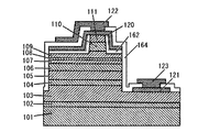
以下、実施例として、図1に示すようなレーザ素子構造について説明する。
実施例1
まず、異種基板として、オフアングル角θ=0.02°、ステップ段差約20オングストローム、テラス幅Wおよそ800オングストロームであり、オリフラ面をA面とし、ステップがA面に垂直であるC面を主面としたサファイア基板101を用意する。
Hereinafter, a laser element structure as shown in FIG. 1 will be described as an example.
Example 1
First, as a dissimilar substrate, an off-angle angle θ = 0.02 °, a step difference of about 20 angstroms, a terrace width W of about 800 angstroms, an orientation flat surface as an A surface, and a step C perpendicular to the A surface are mainly used. A
このサファイア基板101を反応容器内にセットし、温度を510℃にして、キャリアガスに水素、原料ガスにアンモニアとTMG(トリメチルガリウム)とを用い、サファイア基板101上にGaNよりなる低温成長のバッファ層を200オングストロームの膜厚で成長させる。
その後、TMGのみ止めて、温度を1050℃まで上昇させ、1050℃になったら、原料ガスにTMG、アンモニアを用い、アンドープのGaNからなるGaN層を2.5μmの膜厚で成長させる。得られたGaN層を、ストライプ幅4μm、窓部の幅16μmに加工する。その後、ストライプ形状に加工されたGaN層上に、アンドープのGaNを20μm程度成長させ、平坦化して、下地層102を形成する。
The
Thereafter, only TMG is stopped, the temperature is raised to 1050 ° C., and when it reaches 1050 ° C., TMG and ammonia are used as source gases, and a GaN layer made of undoped GaN is grown to a thickness of 2.5 μm. The obtained GaN layer is processed to have a stripe width of 4 μm and a window width of 16 μm. Thereafter, on the GaN layer processed into a stripe shape, undoped GaN is grown to a thickness of about 20 μm and planarized to form the
次に、下地層102の上に、温度を1100℃にして、TMG、TMA(トリメチルアルミニウム)、アンモニアを用い、Al0.02Ga0.98Nからなるバッファ層(図示せず)を0.5μmの膜厚で成長させる。
得られたバッファ層の上に1100℃でSiドープしたAl0.02Ga0.98Nよりなるn型コンタクト層103を4μmの膜厚で成長させる。
Next, a buffer layer (not shown) made of Al 0.02 Ga 0.98 N is formed on the
On the obtained buffer layer, an n-
次に、TMG、TMI(トリメチルインジウム)、アンモニアを用い、温度を920℃にしてSiを5×10¹⁸/cm3ドープしたIn0.10Ga0.90Nよりなるクラック防止層104を0.15μmの膜厚で成長させる。
温度を1000℃にして、アンドープのAl0.07Ga0.93NよりなるA層を25Åの膜厚で成長させ、続いて、不純物ガスとしてシランガスを用い、Siを5×10¹⁸/cm3ドープしたGaNよりなるB層を25Åの膜厚で成長させる。そして、A層、B層を交互に積層する操作をそれぞれ400回繰り返してA層とB層を積層し、総膜厚2μmの多層膜(超格子構造)よりなるn型クラッド層105を成長させる。
Next, the
At a temperature of 1000 ° C., an A layer made of undoped Al 0.07 Ga 0.93 N is grown to a thickness of 25 mm, and then Si is used at 5 × 10 18 / cm 3 using silane gas as an impurity gas. A B layer made of doped GaN is grown to a thickness of 25 mm. Then, the operation of alternately laminating the A layer and the B layer is repeated 400 times to laminate the A layer and the B layer, and the n-type clad
なお、n型クラッド層は超格子構造でなくてもよく、例えば、SiドープのAl0.035Ga0.965N(膜厚2μm)で形成されていてもよい。
クラッド層105の上に、同様の温度で、GaNからなる膜厚0.15μmのn型光ガイド層106を成長させる。
次に、温度を970℃にして、SiドープのIn0.02Ga0.98Nよりなる障壁層(140Å)、アンドープのIn0.1Ga0.9Nよりなる井戸層(70Å)、アンドープのIn0.02Ga0.98Nよりなる障壁層(140Å)をこの順に積層し、さらにこの上に、井戸層と障壁層とを1層ずつ積層し、量子井戸構造の活性層107を形成する。
The n-type cladding layer may not have a superlattice structure, and may be formed of, for example, Si-doped Al 0.035 Ga 0.965 N (film thickness: 2 μm).
On the
Next, at a temperature of 970 ° C., a barrier layer (140Å) made of Si-doped In 0.02 Ga 0.98 N, a well layer (70Å) made of undoped In 0.1 Ga 0.9 N, and undoped Of In 0.02 Ga 0.98 N are stacked in this order, and a well layer and a barrier layer are stacked on top of each other to form an
活性層107の上に、同様の温度で、不純物ガスとしてCp2Mg(シクロペンタジエニルマグネシウム)を用い、Mgを1×10¹⁹/cm3ドープしたAl0.25Ga0.75Nよりなるp型電子閉込め層108を10nmの膜厚で成長させる。
温度を1000℃にして、GaNからなる膜厚0.15μmのp型光ガイド層109を成長させる。このp型光ガイド層109は、p型電子閉込め層108、後述するp型クラッド層110等の隣接層からのMgの拡散により、Mgがドープされるため、アンドープで形成しても、Mgドープ層とできる。
The
The p-type
続いて、1000℃でアンドープAl0.1Ga0.9NよりなるA層を25Åの膜厚で成長させ、MgドープGaNよりなるB層を25Åの膜厚で成長させ、A層、B層を交互に積層する操作を90回繰り返して総膜厚0.45μmの超格子層よりなるp型クラッド層110を成長させる。
なお、p型クラッド層は超格子構造でなくてもよく、例えば、MgドープのAl0.05Ga0.95N(膜厚0.45μm)で形成されていてもよい。
Subsequently, an A layer made of undoped Al 0.1 Ga 0.9 N is grown to a thickness of 25 mm at 1000 ° C., and a B layer made of Mg-doped GaN is grown to a thickness of 25 mm to form an A layer and a B layer. The p-
Note that the p-type cladding layer may not have a superlattice structure, and may be formed of Mg-doped Al 0.05 Ga 0.95 N (film thickness 0.45 μm), for example.
最後に、1000℃で、p型クラッド層110の上に、Mgを1×10²⁰/cm3ドープしたp型GaNよりなるp型コンタクト層111を150Åの膜厚で成長させる。p型コンタクト層111は1×1017/cm3以上の高キャリア濃度とすることが望ましい。
反応容器内で、ウェハを窒素雰囲気中、700℃でアニーリングを行い、p型層をさらに低抵抗化する。
Finally, a p-
In the reaction vessel, the wafer is annealed at 700 ° C. in a nitrogen atmosphere to further reduce the resistance of the p-type layer.
このようにして窒化物半導体を成長させて積層構造体を形成した後、ウェハを反応容器から取り出し、最上層のp型コンタクト層111から、p型半導体層、活性層、n型半導体層の一部を順次エッチングし、n電極を形成するn型コンタクト層の表面を露出させる。また、この際、n電極を形成する領域のみならず、ストライプ状の導波路領域に垂直な端面が露出するようにエッチングすることで、この面を共振器面とすることができる。この共振器面形成工程は、n型コンタクト層露出時と同時に行ってもよく、あるいは別工程で行ってもよい。
After the nitride semiconductor is grown in this way to form a laminated structure, the wafer is taken out of the reaction vessel, and one of the p-type semiconductor layer, the active layer, and the n-type semiconductor layer is removed from the uppermost p-
次に、最上層のp型コンタクト層(上部コンタクト層)111のほぼ全面に、Si酸化物(主として、SiO2)よりなる第1の保護膜を0.5μmの膜厚で形成し、この第1の保護膜をストライプ幅1.6μmに加工する。続いて、第1の保護膜をマスクとして用いて、p型コンタクト層111およびp型クラッド層110、p型光ガイド層109の一部をエッチングして、p型光ガイド層109の膜厚が0.1μmとなる深さまでエッチングすることにより、リッジストライプを形成する。
Next, a first protective film made of Si oxide (mainly SiO 2 ) is formed to a thickness of 0.5 μm on almost the entire surface of the uppermost p-type contact layer (upper contact layer) 111. 1 protective film is processed to a stripe width of 1.6 μm. Subsequently, using the first protective film as a mask, the p-
第1の保護膜の上に、スパッタ装置を利用して、ジルコニウムからなるターゲットと、スパッタガスとしてアルゴンとを用い、RFパワー170Wにて、700Åの下層膜と、RFパワーを100Wにて、300Åの上層膜とを形成し、得られた上下膜を酸素雰囲気下で、600℃にて20分間熱酸化した。
次に、ウェハをフッ酸に浸漬し、第1の保護膜をリフトオフ法により除去する。これにより、p型コンタクト層111の上に設けられていた第1の保護膜が除去されて、p型コンタクト層が露出され、リッジの両側及びp型光ガイド層109の上面に、酸化ジルコニウム2層の積層膜からなる埋め込み膜162を形成した。
On the first protective film, using a sputtering apparatus, a target made of zirconium and argon as a sputtering gas, an RF power of 170 W, an underlayer film of 700 RF, and an RF power of 100 W, 300 Å The upper and lower films obtained were thermally oxidized at 600 ° C. for 20 minutes in an oxygen atmosphere.
Next, the wafer is immersed in hydrofluoric acid, and the first protective film is removed by a lift-off method. As a result, the first protective film provided on the p-
得られた埋め込み膜162を分光エリプソメータ(J.A.WOOLLAM社製のHS−190)で評価したところ、下層膜の屈折率は400nmの光に対して約1.98、上層膜の屈折率は約2.23であった。また、分光エリプソメータでのラフネス(表面粗さ)は、下層膜ではプラスの値が測定され、上層膜ではゼロが測定され、下層膜が上層膜よりも表面粗さが粗いことが確認された。さらに、ウェハ面内での酸素の分布が、酸化ジルコニウムのターゲットを用いて成膜した埋め込み膜に比較して、均一であり、かつ抑えられていることが確認された。
When the obtained embedded
加えて、埋め込み膜162の断面をSEM及びTEMで観察したところ、下層膜と上層膜との界面が鮮明に観察され、さらに、下層膜は粒が細かく、上層膜は粒が粗く角が認められた。
続いて、リッジ上面の露出したp型コンタクト層111の表面及び埋め込み膜162の上に、Ni/Au(100Å/1500Å)よりなるp電極120を形成する。p電極120はストライプ幅を30μmとして、図1に示すように、第2の保護膜162の上に渡って形成する。
In addition, when the cross section of the buried
Subsequently, a p-
このp電極120の形成の前又は後に、既に露出させたn型コンタクト層103の表面に、Ti/Al(100Å/5000Å)よりなるストライプ状のn電極121をストライプと平行な方向で形成する。
次に、p電極120及びn電極121上に、所望の形状のマスクを形成し、SiO2単層からなる膜164を設ける。
Before or after the formation of the p-
Next, a mask having a desired shape is formed on the p-
その後、p電極120上にNi−Ti−Au(1000Å−1000Å−8000Å)よりなるパッド電極122を設け、n電極121上にNi−Ti−Au(1000Å−1000Å−8000Å)よりなるパッド電極123を設ける。
以上のようにして、n電極121とp電極120とを形成した後、上述したn型コンタクト層の露出面の一部をさらにエッチングしてサファイアを露出させる。次いで、、SiO2からなる膜164を除去し、ウェハのサファイア基板101を研磨して200μmとする。
Thereafter, a
After forming the
続いて、ウェハをバー状に分割し、さらに、少なくとも、主レーザ光の出射面側に、活性層で発光する光を効率よく共振させ、特に反対面側の共振器面が、光出射面側の共振器面と屈折率差を有するように、スパッタ装置を用いて、Al2O3からなる保護膜を形成する。次いで、反対面側の共振器面には、Al2O3の上に(SiO2/ZrO2)を3回繰り返し積層した合計7層からなる誘電体多層膜(図示せず)を形成した。 Subsequently, the wafer is divided into bars, and at least the light emitted from the active layer is efficiently resonated at least on the light emitting surface side of the main laser light. A protective film made of Al 2 O 3 is formed using a sputtering apparatus so as to have a refractive index difference from the resonator surface. Next, a dielectric multilayer film (not shown) composed of a total of seven layers in which (SiO 2 / ZrO 2 ) was repeatedly layered three times on Al 2 O 3 was formed on the opposite resonator surface.
最後に、p電極に平行な方向で、ウェハをチップ状に分割してレーザ素子(共振器長は650μm)を得た。
得られたレーザ素子について、埋め込み膜とp電極との密着性を評価した。まず、得られた半導体装置を、超音波での30分間の処理に2回付した後、超音波で30分間処理し、180℃で30分間熱処理し、さらに冷水に浸漬し、この処理を3回行った。その後、超音波で60分間処理し、220〜300℃で30分間熱処理し、さらに冷水に浸漬し、この処理を8回行い、最後に超音波で60分間処理した。
このような一連の超音波処理及び熱衝撃試験によっても、p型電極の剥がれは見られず、その後の製造プロセスにも十分に耐えることができることが確認された。
Finally, the wafer was divided into chips in the direction parallel to the p-electrode to obtain a laser element (resonator length 650 μm).
About the obtained laser element, the adhesiveness of a buried film and a p electrode was evaluated. First, the obtained semiconductor device was subjected to ultrasonic treatment for 30 minutes twice, then treated with ultrasonic waves for 30 minutes, heat-treated at 180 ° C. for 30 minutes, and further immersed in cold water. I went twice. Then, it processed for 60 minutes with ultrasonic waves, heat-processed for 30 minutes at 220-300 degreeC, and also immersed in cold water, this process was performed 8 times, and finally, it processed with ultrasonic waves for 60 minutes.
Even by such a series of ultrasonic treatment and thermal shock test, it was confirmed that the p-type electrode was not peeled off and could sufficiently withstand the subsequent manufacturing process.
一方、比較のため、下層膜を1000Åとし、上層膜を形成しない単層の埋め込み膜を形成する以外、上述した実施例と同様にレーザ素子を形成し、同様に超音波処置及び熱衝撃試験を行った。
その結果、最初の30分間の超音波処理及び熱衝撃試験で、p型電極が剥がれることが確認された。
On the other hand, for comparison, except that the lower layer film is set to 1000 mm and a single-layer buried film not forming the upper layer film is formed, a laser element is formed in the same manner as in the above-described embodiment, and ultrasonic treatment and thermal shock test are similarly performed. went.
As a result, it was confirmed that the p-type electrode was peeled off in the first 30 minutes of ultrasonic treatment and thermal shock test.
また、得られたレーザ素子においては、埋め込み膜が、異なる2層の屈折率を有するように構成されており、つまり、導波路に近い側から低屈折率、高屈折率の埋め込み膜が形成されているため、発せられる光の基本モードのみを閉じ込めて、高次モードを導波路の外に逃がして電極に吸収させることができる。その結果、所望のFFPを得ることが可能となる。
さらに、得られたレーザ素子における埋め込み膜は、p型窒化物半導体層側において、密度が低く構成されているため、それに起因してp型窒化物半導体層側においてのみ誘電率を低下させることができる。これにより、より高速での応答に寄与することが可能となる。
Further, in the obtained laser element, the buried film is configured to have two different refractive indexes, that is, a buried film having a low refractive index and a high refractive index is formed from the side close to the waveguide. Therefore, only the fundamental mode of emitted light can be confined, and higher-order modes can escape from the waveguide and be absorbed by the electrode. As a result, a desired FFP can be obtained.
Furthermore, since the buried film in the obtained laser element is configured to have a low density on the p-type nitride semiconductor layer side, the dielectric constant can be lowered only on the p-type nitride semiconductor layer side. it can. Thereby, it becomes possible to contribute to the response at higher speed.
実施例2
まず、実施例1と同様のサファイア基板101を用意する。
Example 2
First, a
このサファイア基板101を反応容器内にセットし、温度を510℃にして、キャリアガスに水素、原料ガスにアンモニアとTMG(トリメチルガリウム)とを用い、サファイア基板101上にGaNよりなる低温成長のバッファ層を200オングストロームの膜厚で成長させる。
その後、TMGのみ止めて、温度を1050℃まで上昇させ、1050℃になったら、原料ガスにTMG、アンモニアを用い、アンドープのGaNからなるGaN層を2.5μmの膜厚で成長させる。得られたGaN層を、ストライプ幅4μm、窓部の幅16μmに加工する。その後、ストライプ形状に加工されたGaN層上に、アンドープのGaNを20μm程度成長させ、平坦化して、下地層102を形成する。
The
Thereafter, only TMG is stopped, the temperature is raised to 1050 ° C., and when it reaches 1050 ° C., TMG and ammonia are used as source gases, and a GaN layer made of undoped GaN is grown to a thickness of 2.5 μm. The obtained GaN layer is processed to have a stripe width of 4 μm and a window width of 16 μm. Thereafter, on the GaN layer processed into a stripe shape, undoped GaN is grown to a thickness of about 20 μm and planarized to form the
次に、下地層102の上に、温度を1100℃にして、TMG、TMA(トリメチルアルミニウム)、アンモニアを用い、Al0.02Ga0.98Nからなるバッファ層(図示せず)を0.5μmの膜厚で成長させる。
得られたバッファ層の上に1100℃でSiドープしたAl0.02Ga0.98Nよりなるn型コンタクト層103を4μmの膜厚で成長させる。
Next, a buffer layer (not shown) made of Al 0.02 Ga 0.98 N is formed on the
On the obtained buffer layer, an n-
次に、TMG、TMI(トリメチルインジウム)、アンモニアを用い、温度を920℃にしてSiを5×10¹⁸/cm3ドープしたIn0.10Ga0.90Nよりなるクラック防止層104を0.15μmの膜厚で成長させる。
温度を1000℃にして、アンドープのAl0.13Ga0.87NよりなるA層を25Åの膜厚で成長させ、続いて、不純物ガスとしてシランガスを用い、Siを5×10¹⁸/cm3ドープしたAl0.09Ga0.91NよりなるB層を25Åの膜厚で成長させる。そして、A層、B層を交互に積層する操作をそれぞれ120回繰り返してA層とB層を積層し、総膜厚0.6μmの多層膜(超格子構造)よりなるn型クラッド層105を成長させる。
Next, the
At a temperature of 1000 ° C., an A layer made of undoped Al 0.13 Ga 0.87 N is grown to a thickness of 25 mm, and subsequently, Si is used as an impurity gas and Si is 5 × 10 18 / cm 3. A B layer made of doped Al 0.09 Ga 0.91 N is grown to a thickness of 25 mm. Then, the operation of alternately laminating the A layer and the B layer is repeated 120 times to laminate the A layer and the B layer, and the n-
クラッド層105の上に、同様の温度で、Al0.065Ga0.935Nからなる膜厚0.15μmのn型光ガイド層106を成長させる。
次に、温度を970℃にして、SiドープのAl0.15Ga0.85Nよりなる障壁層(70Å)、アンドープのIn0.02Al0.03Ga0.95Nよりなる井戸層(100Å)、アンドープのAl0.15Ga0.85Nよりなる障壁層(50Å)をこの順に積層し、量子井戸構造の活性層107を形成する。
On the
Next, at a temperature of 970 ° C., a barrier layer (70 cm) made of Si-doped Al 0.15 Ga 0.85 N and a well layer made of undoped In 0.02 Al 0.03 Ga 0.95 N ( 100Å) and a barrier layer (50Å) made of undoped Al 0.15 Ga 0.85 N are stacked in this order to form an
活性層107の上に、同様の温度で、不純物ガスとしてCp2Mg(シクロペンタジエニルマグネシウム)を用い、Mgを1×10¹⁹/cm3ドープしたAl0.3Ga0.7Nよりなるp型電子閉込め層108を13nmの膜厚で成長させる。
温度を1000℃にして、Al0.065Ga0.935Nからなる膜厚0.15μmのp型光ガイド層109を成長させる。このp型光ガイド層109は、p型電子閉込め層108、後述するp型クラッド層110等の隣接層からのMgの拡散により、Mgがドープされるため、アンドープで形成しても、Mgドープ層とできる。
The
The p-type
続いて、1000℃でアンドープAl0.13Ga0.87NよりなるA層を25Åの膜厚で成長させ、MgドープAl0.09Ga0.91NよりなるB層を25Åの膜厚で成長させ、A層、B層を交互に積層する操作を90回繰り返して総膜厚0.45μmの超格子層よりなるp型クラッド層110を成長させる。
最後に、1000℃で、p型クラッド層110の上に、Mgを1×10²⁰/cm3ドープしたp型GaNよりなるp型コンタクト層111を150Åの膜厚で成長させる。p型コンタクト層111は1×1017/cm3以上の高キャリア濃度とすることが望ましい。
Subsequently, an A layer made of undoped Al 0.13 Ga 0.87 N is grown to a thickness of 25 mm at 1000 ° C., and a B layer made of Mg doped Al 0.09 Ga 0.91 N is grown to a thickness of 25 mm. The p-
Finally, a p-
反応容器内で、ウェハを窒素雰囲気中、700℃でアニーリングを行い、p型層をさらに低抵抗化する。
このようにして窒化物半導体を成長させて積層構造体を形成した後、ウェハを反応容器から取り出し、最上層のp型コンタクト層111から、p型半導体層、活性層、n型半導体層の一部を順次エッチングし、n電極を形成するn型コンタクト層の表面を露出させる。また、この際、n電極を形成する領域のみならず、共振面も同時に形成する。このように、後工程において窒化物半導体素子に劈開又は分割する位置及び/又はその周辺を含む領域においても、n型コンタクト層の表面を露出させることで、応力を緩和する等の効果を得られる場合がある。
In the reaction vessel, the wafer is annealed at 700 ° C. in a nitrogen atmosphere to further reduce the resistance of the p-type layer.
After the nitride semiconductor is grown in this way to form a laminated structure, the wafer is taken out of the reaction vessel, and one of the p-type semiconductor layer, the active layer, and the n-type semiconductor layer is removed from the uppermost p-
次に、最上層のp型コンタクト層(上部コンタクト層)111のほぼ全面に、Si酸化物(主として、SiO2)よりなる第1の保護膜を0.5μmの膜厚で形成し、この第1の保護膜をストライプ幅1.6μmに加工する。続いて、第1の保護膜をマスクとして用いて、p型コンタクト層111およびp型クラッド層110、p型光ガイド層109の一部をエッチングして、p型光ガイド層109の膜厚が0.1μmとなる深さまでエッチングすることにより、リッジストライプを形成する。
第1の保護膜の上に、スパッタ装置を利用して、ジルコニウムからなるターゲットと、スパッタガスとしてアルゴンとを用い、RFパワー170Wにて、1700Åの下層膜と、RFパワーを100Wにて、300Åの上層膜とを形成し、得られた上下膜を酸素雰囲気下で、600℃にて20分間熱酸化した。
Next, a first protective film made of Si oxide (mainly SiO 2 ) is formed to a thickness of 0.5 μm on almost the entire surface of the uppermost p-type contact layer (upper contact layer) 111. 1 protective film is processed to a stripe width of 1.6 μm. Subsequently, using the first protective film as a mask, the p-
On the first protective film, using a sputtering apparatus, a target made of zirconium and argon as a sputtering gas, an RF power of 170 W, an underlayer film of 1700 mm, and an RF power of 100 W, 300 mm The upper and lower films obtained were thermally oxidized at 600 ° C. for 20 minutes in an oxygen atmosphere.
次に、ウェハをフッ酸に浸漬し、第1の保護膜をリフトオフ法により除去する。これにより、p型コンタクト層111の上に設けられていた第1の保護膜が除去されて、p型コンタクト層が露出され、リッジの両側及びp型光ガイド層109の上面に、酸化ジルコニウム2層の積層膜からなる埋め込み膜162を形成した。
得られた埋め込み膜162を分光エリプソメータ(J.A.WOOLLAM社製のHS−190)で評価したところ、下層膜の屈折率は400nmの光に対して約1.98、上層膜の屈折率は約2.23であった。また、分光エリプソメータでのラフネス(表面粗さ)は、下層膜ではプラスの値が測定され、上層膜ではゼロが測定され、下層膜が上層膜よりも表面粗さが粗いことが確認された。さらに、ウェハ面内での酸素の分布が、酸化ジルコニウムのターゲットを用いて成膜した埋め込み膜に比較して、均一であり、かつ抑えられていることが確認された。
Next, the wafer is immersed in hydrofluoric acid, and the first protective film is removed by a lift-off method. As a result, the first protective film provided on the p-
When the obtained embedded
加えて、埋め込み膜162の断面をSEM及びTEMで観察したところ、下層膜と上層膜との界面が鮮明に観察され、さらに、下層膜は粒が細かく、上層膜は粒が粗く角が認められた。
続いて、リッジ上面の露出したp型コンタクト層111の表面及び埋め込み膜162の上に、Ni/Au/Pt(100Å/1500Å/1500Å)よりなるp電極120を形成する。p電極120はストライプ幅を30μmとして、図1に示すように、第2の保護膜162の上に渡って形成する。
In addition, when the cross section of the buried
Subsequently, a p-
このp電極120の形成の前又は後に、既に露出させたn型コンタクト層103の表面に、Ti/Al(100Å/5000Å)よりなるストライプ状のn電極121をストライプと平行な方向で形成する。
次に、p電極120及びn電極121上に、所望の形状のマスクを形成し、SiO2よりなる単層膜164を設ける。
続いて、Ti/Pt(100Å/500Å)よりなる密着層を形成する。
Before or after the formation of the p-
Next, a mask having a desired shape is formed on the p-
Subsequently, an adhesion layer made of Ti / Pt (100/500) is formed.
その後、p電極120上にPt/Au(3000Å/6000Å)よりなるパッド電極122を設け、n電極121上にNi−Ti−Au(1000Å−1000Å−8000Å)よりなるパッド電極123を設ける。
以上のようにして、n電極121とp電極120とを形成した後、ウェハのサファイア基板101を研磨して200μmとした後、上述したn型コンタクト層の一部をさらにエッチングして基板を露出させる。次いで、SiO2からなる膜を除去し、ウエハのサファイア基板を研磨して200μmの厚さとする。
続いて、少なくとも、主レーザ光の出射面側に、活性層で発光する光を効率よく共振させ、特に反対面側の共振器面が、光出射面側の共振器面と屈折率差を有するように、スパッタ装置を用いて、Nb2O5またはAl2O3からなる保護膜を形成し、次いで、光反射側の共振器面には、ZrO2またはAl2O3の上に、(SiO2/ZrO2)を4回繰り返し積層した合計9層からなる誘電体多層膜(図示せず)を形成した。 最後に、p電極に平行な方向で、ウェハをチップ状に切断してレーザ素子(共振器長は650μm)を得た。
Thereafter, a
After forming the n-
Subsequently, the light emitted from the active layer is efficiently resonated at least on the emission surface side of the main laser beam, and in particular, the resonator surface on the opposite surface side has a refractive index difference from the resonator surface on the light emission surface side. Thus, using a sputtering apparatus, a protective film made of Nb 2 O 5 or Al 2 O 3 is formed, and then on the resonator surface on the light reflection side, on ZrO 2 or Al 2 O 3 , ( A dielectric multilayer film (not shown) composed of a total of nine layers in which SiO 2 / ZrO 2 ) was repeatedly laminated four times was formed. Finally, the wafer was cut into chips in a direction parallel to the p-electrode to obtain a laser element (resonator length: 650 μm).
得られたレーザ素子について、埋め込み膜とp電極との密着性を実施例1と同様に評価した。その結果、p型電極の剥がれは見られず、その後の製造プロセスにも十分に耐えることができることが確認された。
一方、比較のため、下層膜を1000Åとし、上層膜を形成しない単層の埋め込み膜を形成する以外、上述した実施例と同様にレーザ素子を形成し、同様に超音波処置及び熱衝撃試験を行った。
For the obtained laser element, the adhesion between the buried film and the p-electrode was evaluated in the same manner as in Example 1. As a result, it was confirmed that the p-type electrode was not peeled off and could sufficiently withstand the subsequent manufacturing process.
On the other hand, for comparison, except that the lower layer film is set to 1000 mm and a single-layer buried film not forming the upper layer film is formed, a laser element is formed in the same manner as in the above-described embodiment, and ultrasonic treatment and thermal shock test are similarly performed. went.
その結果、最初の30分間の超音波処理及び熱衝撃試験で、p型電極が剥がれることが確認された。
また、得られたレーザ素子においては、埋め込み膜が、異なる2層の屈折率を有するように構成されており、つまり、導波路に近い側から低屈折率、高屈折率の埋め込み膜が形成されているため、発せられる光の基本モードのみを閉じ込めて、高次モードを導波路の外に逃がして電極に吸収させることができる。その結果、所望のFFPを得ることが可能となる。
さらに、得られたレーザ素子における埋め込み膜は、p型窒化物半導体層側において、密度が低く構成されているため、それに起因してp型窒化物半導体層側においてのみ誘電率を低下させることができる。これにより、より高速での応答に寄与することが可能となる。
As a result, it was confirmed that the p-type electrode was peeled off in the first 30 minutes of ultrasonic treatment and thermal shock test.
Further, in the obtained laser element, the buried film is configured to have two different refractive indexes, that is, a buried film having a low refractive index and a high refractive index is formed from the side close to the waveguide. Therefore, only the fundamental mode of emitted light can be confined, and higher-order modes can escape from the waveguide and be absorbed by the electrode. As a result, a desired FFP can be obtained.
Furthermore, since the buried film in the obtained laser element is configured to have a low density on the p-type nitride semiconductor layer side, the dielectric constant can be lowered only on the p-type nitride semiconductor layer side. it can. Thereby, it becomes possible to contribute to the response at higher speed.
実施例3
この実施例のレーザ素子は、埋め込み膜162を、まず、下層膜として、ジルコニウムからなるターゲットと、アルゴンガスのスパッタガスとを用いて成膜し、上層膜として、アルゴンガスと酸素ガスとの混合ガスをスパッタガスとして用いて、酸化ジルコニウムの2層積層膜を形成し、その後、同様に熱処理を行うことにより形成した以外は、実質的に実施例1と同様の方法により、同様の構成のレーザ素子を得た。
なお、下層膜の成膜時のスパッタガスの圧力は0.1〜2.0Pa程度であり、上層膜の成膜時の酸素ガスの分圧は、1×10⁻³〜1×10⁻¹Pa程度とした。
得られたレーザ素子は、実施例1と同様に、酸素の面内分布が均一で電極との密着性が良好であることが確認された。
Example 3
In the laser element of this embodiment, the buried
Note that the pressure of the sputtering gas when forming the lower layer film is about 0.1 to 2.0 Pa, and the partial pressure of the oxygen gas when forming the upper layer film is 1 × 10 −3 to 1 × 10 −1. About Pa.
As in Example 1, the obtained laser element was confirmed to have a uniform in-plane oxygen distribution and good adhesion to the electrode.
実施例4
この実施例のレーザ素子は、埋め込み膜162を、スパッタ法にて、まず、下層膜として、ジルコニウムからなるターゲットと、アルゴンガスのスパッタガスとを用い、圧力を1.5pa程度で610Åの膜厚で成膜し、次いで、上層膜として、同じターゲット及びスパッタガスを用いて、圧力0.1pa程度で320Åの膜厚で成膜して、酸化ジルコニウムの2層積層膜を形成した以外は、実質的に実施例1と同様の方法により、同様の構成のレーザ素子を得た。
Example 4
In the laser element of this embodiment, the buried
得られた上層膜及び下層膜について、X線解折により密度を測定したところ、上層膜では約5.7g/cm、下層膜では4.19g/cmであり、上層膜は下層膜よりも緻密な構造を有していることが確認された。
また、得られたレーザ素子は、実施例1と同様に、酸素の面内分布が均一で電極との密着性が良好であることが確認された。
When the density of the obtained upper layer film and lower layer film was measured by X-ray diffraction, it was about 5.7 g / cm for the upper layer film and 4.19 g / cm for the lower layer film, and the upper layer film was denser than the lower layer film. It was confirmed that it has a simple structure.
In addition, it was confirmed that the obtained laser element had a uniform oxygen in-plane distribution and good adhesion to the electrode, as in Example 1.
実施例5
この実施例のレーザ素子は、埋め込み膜162を、スパッタ法にて、まず、ジルコニウムからなるターゲットと、アルゴンガスのスパッタガスとを用いて、圧力を1.5pa程度で成膜し、徐々に圧力を0.1pa程度まで低下させ、総膜厚を1000Åとなるように成膜して、酸化ジルコニウムの2層積層膜を形成した以外は、実質的に実施例1と同様の方法により、同様の構成のレーザ素子を得た。
Example 5
In the laser element of this embodiment, the buried
得られた埋め込み膜について、X線解折により密度を測定したところ、表面側の極薄い膜厚の部分では約5.7g/cm、p型窒化物半導体層側の極薄い部分では4.19g/cmであり、p型窒化物半導体層側から、表面側にかけて緻密さが増す構造を有していることが確認された。
また、得られたレーザ素子は、実施例1と同様に、酸素の面内分布が均一で電極との密着性が良好であることが確認された。
When the density of the buried film thus obtained was measured by X-ray diffraction, it was about 5.7 g / cm at the extremely thin part on the surface side and 4.19 g at the extremely thin part on the p-type nitride semiconductor layer side. / Cm, and it was confirmed to have a structure in which the density increases from the p-type nitride semiconductor layer side to the surface side.
In addition, it was confirmed that the obtained laser element had a uniform oxygen in-plane distribution and good adhesion to the electrode, as in Example 1.
実施例6
この実施例のレーザ素子は、埋め込み膜162を、まず、下層膜として、スパッタ法に代えて、真空蒸着法を利用する以外は、実質的に実施例1と同様の方法により、同様の構成のレーザ素子を得た。
得られたレーザ素子は、実施例1と同様に、酸素の面内分布が均一で電極との密着性が良好であることが確認された。
Example 6
The laser device of this example has the same configuration as that of Example 1 except that the buried
As in Example 1, the obtained laser element was confirmed to have a uniform in-plane oxygen distribution and good adhesion to the electrode.
実施例7
この実施例のレーザ素子は、埋め込み膜162を、まず、下層膜を成膜する際に、イオン銃を利用して、ウェハ表面(p型半導体層)に酸素イオンを1012個/cm2程度で照射する以外は、実質的に実施例5と同様の方法により、同様の構成のレーザ素子を得た。
得られたレーザ素子は、実施例1と同様に、酸素の面内分布が均一で電極との密着性が良好であることが確認された。
Example 7
In the laser element of this embodiment, when the buried
As in Example 1, the obtained laser element was confirmed to have a uniform in-plane oxygen distribution and good adhesion to the electrode.
実施例8
この実施例のレーザ素子は、埋め込み膜162を、まず、下層膜を成膜する際に、真空蒸着法により成膜レートを50Å/秒とし、上層膜を成膜する際に、真空蒸着法により成膜レートを5Å/秒に減少させて、酸化ジルコニウムの2層積層膜を形成する以外は、実質的に実施例1と同様の方法により、同様の構成のレーザ素子を得た。
得られたレーザ素子は、実施例1と同様に、酸素の面内分布が均一で電極との密着性が良好であることが確認された。
Example 8
In the laser element of this embodiment, the buried
As in Example 1, the obtained laser element was confirmed to have a uniform in-plane oxygen distribution and good adhesion to the electrode.
実施例9
この実施例のレーザ素子は、図2に示すように、埋め込み膜62を、まず、下層膜aを成膜する際に、真空蒸着法により成膜レートを5Å/秒として酸化ジルコニウムを100Åの膜厚で、中層膜bは、スパッタ法により、Al2O3、HfO2又はSiO2を700Åの膜厚で、上層膜cは、真空蒸着法により成膜レートを5Å/秒として200Åの膜厚で酸化ジルコニウムを形成する以外は、実質的に実施例1と同様の方法により、同様の構成のレーザ素子を得た。
得られたレーザ素子は、実施例1の効果に加えて、埋め込み膜62の絶縁耐性をより確保することができ、さらに信頼性の高いレーザ素子を得ることができる。
Example 9
As shown in FIG. 2, in the laser element of this embodiment, when the buried
In addition to the effects of the first embodiment, the obtained laser element can further ensure the insulation resistance of the buried
実施例10
まず、実施例1と同様のサファイア基板を用意する。
このサファイア基板を反応容器内にセットし、温度を510℃にして、キャリアガスに水素、原料ガスにアンモニアとTMG(トリメチルガリウム)とを用い、サファイア基板上にGaNよりなる低温成長のバッファ層を200オングストロームの膜厚で成長させる。その後、TMGのみ止めて、温度を1050℃まで上昇させ、1050℃になったら、原料ガスにTMG、アンモニアを用い、アンドープのGaNからなるGaN層を2.5μmの膜厚で成長させる。
得られたGaN層を、ストライプ幅4μm、窓部の幅16μmに加工する。その後、ストライプ形状に加工されたGaN層上に、アンドープのGaNを20μm程度成長させ、平坦化して、下地層を形成する。下地層を成長した後、ウェハを反応容器から取り出し、この下地層の表面に、ストライプ状のフォトマスクを形成し、CVD装置によりストライプ幅10〜300μm、ストライプ間隔(窓部)5〜300μmのSiO2よりなる保護膜を形成する。
保護膜を形成した後、ウェハをHVPE(ハイドライド気相成長法)装置に移送し、原料にGaメタル、HClガス及びアンモニアを用い、GaNよりなる窒化物半導体を100μmの膜厚で成長させる。
このとき、裏面にn電極を形成する場合には、酸素又はSiドープでGaNを成長させる。また、表面にn電極を形成する場合にはノンドープでもよい。
Example 10
First, the same sapphire substrate as in Example 1 is prepared.
This sapphire substrate is set in a reaction vessel, the temperature is set to 510 ° C., hydrogen is used as a carrier gas, ammonia and TMG (trimethyl gallium) are used as a source gas, and a low-temperature growth buffer layer made of GaN is formed on the sapphire substrate. Grow with a film thickness of 200 Å. Thereafter, only TMG is stopped, the temperature is raised to 1050 ° C., and when it reaches 1050 ° C., TMG and ammonia are used as source gases, and a GaN layer made of undoped GaN is grown to a thickness of 2.5 μm.
The obtained GaN layer is processed to have a stripe width of 4 μm and a window width of 16 μm. Thereafter, undoped GaN is grown on the GaN layer processed into a stripe shape by about 20 μm, and is flattened to form an underlayer. After the underlayer is grown, the wafer is taken out of the reaction vessel, a striped photomask is formed on the surface of the underlayer, and a SiO 2 having a stripe width of 10 to 300 μm and a stripe interval (window) of 5 to 300 μm is formed by a CVD apparatus. 2 is formed.
After forming the protective film, the wafer is transferred to an HVPE (hydride vapor phase epitaxy) apparatus, and a nitride semiconductor made of GaN is grown to a thickness of 100 μm using Ga metal, HCl gas and ammonia as raw materials.
At this time, when an n-electrode is formed on the back surface, GaN is grown by oxygen or Si doping. Further, when an n-electrode is formed on the surface, it may be non-doped.
次に、成長させたGaN層の上に、温度を1100℃にして、TMG、TMA(トリメチルアルミニウム)、アンモニアを用い、Al0.02Ga0.98Nからなるバッファ層(図示せず)を0.5μmの膜厚で成長させる。
表面にn電極を形成する場合には、得られたバッファ層の上に1100℃でSiドープしたAl0.02Ga0.98Nよりなるn型コンタクト層103を4μmの膜厚で成長させる。
Next, a buffer layer (not shown) made of Al 0.02 Ga 0.98 N is used on the grown GaN layer at a temperature of 1100 ° C. using TMG, TMA (trimethylaluminum), and ammonia. Growing with a film thickness of 0.5 μm.
When forming an n-electrode on the surface, an n-
温度を1000℃にして、アンドープのAl0.07Ga0.93NよりなるA層を25Åの膜厚で成長させ、続いて、不純物ガスとしてシランガスを用い、Siを5×10¹⁸/cm3ドープしたGaNよりなるB層を25Åの膜厚で成長させる。そして、A層、B層を交互に積層する操作をそれぞれ400回繰り返してA層とB層を積層し、総膜厚2μmの多層膜(超格子構造)よりなるn型クラッド層を成長させる。 At a temperature of 1000 ° C., an A layer made of undoped Al 0.07 Ga 0.93 N is grown to a thickness of 25 mm, and then Si is used at 5 × 10 18 / cm 3 using silane gas as an impurity gas. A B layer made of doped GaN is grown to a thickness of 25 mm. Then, the operation of alternately laminating the A layer and the B layer is repeated 400 times to laminate the A layer and the B layer, and an n-type cladding layer made of a multilayer film (superlattice structure) having a total film thickness of 2 μm is grown.
なお、n型クラッド層は超格子構造でなくてもよく、例えば、SiドープのAl0.035Ga0.965N(膜厚2μm)で形成されていてもよい。
クラッド層の上に、同様の温度で、GaNからなる膜厚0.15μmのn型光ガイド層を成長させる。
次に、温度を970℃にして、SiドープのIn0.02Ga0.98Nよりなる障壁層(140Å)、アンドープのIn0.1Ga0.9Nよりなる井戸層(70Å)、アンドープのIn0.02Ga0.98Nよりなる障壁層(140Å)をこの順に積層し、さらにこの上に、井戸層と障壁層とを1層ずつ積層し、量子井戸構造の活性層を形成する。
The n-type cladding layer may not have a superlattice structure, and may be formed of, for example, Si-doped Al 0.035 Ga 0.965 N (film thickness: 2 μm).
On the clad layer, an n-type light guide layer made of GaN having a thickness of 0.15 μm is grown at the same temperature.
Next, at a temperature of 970 ° C., a barrier layer (140Å) made of Si-doped In 0.02 Ga 0.98 N, a well layer (70Å) made of undoped In 0.1 Ga 0.9 N, and undoped Of In 0.02 Ga 0.98 N are stacked in this order, and a well layer and a barrier layer are stacked one by one to form an active layer having a quantum well structure. .
活性層の上に、同様の温度で、不純物ガスとしてCp2Mg(シクロペンタジエニルマグネシウム)を用い、Mgを1×10¹⁹/cm3ドープしたAl0.25Ga0.75Nよりなるp型電子閉込め層を10nmの膜厚で成長させる。
温度を1000℃にして、GaNからなる膜厚0.15μmのp型光ガイド層109を成長させる。このp型光ガイド層は、p型電子閉込め層、後述するp型クラッド層等の隣接層からのMgの拡散により、Mgがドープされるため、アンドープで形成しても、Mgドープ層とできる。
On the active layer, p is made of Al 0.25 Ga 0.75 N doped with 1 × 10 19 / cm 3 of Mg using Cp 2 Mg (cyclopentadienyl magnesium) as an impurity gas at the same temperature. A type electron confinement layer is grown to a thickness of 10 nm.
The p-type
続いて、1000℃でアンドープAl0.1Ga0.9NよりなるA層を25Åの膜厚で成長させ、MgドープGaNよりなるB層を25Åの膜厚で成長させ、A層、B層を交互に積層する操作を90回繰り返して総膜厚0.45μmの超格子層よりなるp型クラッド層を成長させる。
なお、p型クラッド層は超格子構造でなくてもよく、例えば、MgドープのAl0.05Ga0.95N(膜厚0.45μm)で形成されていてもよい。
Subsequently, an A layer made of undoped Al 0.1 Ga 0.9 N is grown to a thickness of 25 mm at 1000 ° C., and a B layer made of Mg-doped GaN is grown to a thickness of 25 mm to form an A layer and a B layer. The p-type cladding layer made of a superlattice layer having a total film thickness of 0.45 μm is grown by repeating the operation of alternately stacking 90 times.
Note that the p-type cladding layer may not have a superlattice structure, and may be formed of Mg-doped Al 0.05 Ga 0.95 N (film thickness 0.45 μm), for example.
最後に、1000℃で、p型クラッド層の上に、Mgを1×10²⁰/cm3ドープしたp型GaNよりなるp型コンタクト層を150Åの膜厚で成長させる。p型コンタクト層は1×1017/cm3以上の高キャリア濃度とすることが望ましい。
反応容器内で、ウェハを窒素雰囲気中、700℃でアニーリングを行い、p型層をさらに低抵抗化する。
このようにして窒化物半導体を成長させて積層構造体を形成した後、ウェハを反応容器から取り出し、最上層のp型コンタクト層111から、p型半導体層、活性層、n型半導体層の一部を順次エッチングし、n電極を形成するn型コンタクト層の表面を露出させる。なお、裏面側にn電極を設ける場合は、この工程は省略することもできる。
Finally, a p-type contact layer made of p-type GaN doped with Mg at 1 × 10 20 / cm 3 is grown on the p-type cladding layer at a temperature of 1000 ° C. to a thickness of 150 mm. The p-type contact layer preferably has a high carrier concentration of 1 × 10 17 / cm 3 or more.
In the reaction vessel, the wafer is annealed at 700 ° C. in a nitrogen atmosphere to further reduce the resistance of the p-type layer.
After the nitride semiconductor is grown in this way to form a laminated structure, the wafer is taken out of the reaction vessel, and one of the p-type semiconductor layer, the active layer, and the n-type semiconductor layer is removed from the uppermost p-
次に、最上層のp型コンタクト層(上部コンタクト層)のほぼ全面に、Si酸化物(主として、SiO2)よりなる第1の保護膜を0.5μmの膜厚で形成し、この第1の保護膜をストライプ幅1.6μmに加工する。続いて、第1の保護膜をマスクとして用いて、p型コンタクト層およびp型クラッド層、p型光ガイド層の一部をエッチングして、p型光ガイド層の膜厚が0.1μmとなる深さまでエッチングすることにより、リッジストライプを形成する。 Next, a first protective film made of Si oxide (mainly SiO 2 ) is formed to a thickness of 0.5 μm on almost the entire surface of the uppermost p-type contact layer (upper contact layer). This protective film is processed to a stripe width of 1.6 μm. Subsequently, using the first protective film as a mask, the p-type contact layer, the p-type cladding layer, and a part of the p-type light guide layer are etched, and the film thickness of the p-type light guide layer becomes 0.1 μm. A ridge stripe is formed by etching to a certain depth.
第1の保護膜の上に、スパッタ装置を利用して、ジルコニウムからなるターゲットと、スパッタガスとしてアルゴンとを用い、RFパワー170Wにて、700Åの下層膜と、RFパワーを100Wにて、300Åの上層膜とを形成し、得られた上下膜を酸素雰囲気下で、600℃にて20分間熱酸化した。
次に、ウェハをフッ酸に浸漬し、第1の保護膜をリフトオフ法により除去する。これにより、p型コンタクト層の上に設けられていた第1の保護膜が除去されて、p型コンタクト層が露出され、リッジの両側及びp型光ガイド層の上面に、酸化ジルコニウム2層の積層膜からなる埋め込み膜が形成された。
On the first protective film, using a sputtering apparatus, a target made of zirconium and argon as a sputtering gas, an RF power of 170 W, an underlayer film of 700 RF, and an RF power of 100 W, 300 Å The upper and lower films obtained were thermally oxidized at 600 ° C. for 20 minutes in an oxygen atmosphere.
Next, the wafer is immersed in hydrofluoric acid, and the first protective film is removed by a lift-off method. As a result, the first protective film provided on the p-type contact layer is removed, and the p-type contact layer is exposed, and two zirconium oxide layers are formed on both sides of the ridge and on the upper surface of the p-type light guide layer. A buried film made of a laminated film was formed.
得られた埋め込み膜を分光エリプソメータ(J.A.WOOLLAM社製のHS−190)で評価したところ、下層膜の屈折率は400nmの光に対して約1.98、上層膜の屈折率は約2.23であった。また、分光エリプソメータでのラフネス(表面粗さ)は、下層膜ではプラスの値が測定され、上層膜ではゼロが測定され、下層膜が上層膜よりも表面粗さが粗いことが確認された。さらに、ウェハ面内での酸素の分布が、酸化ジルコニウムのターゲットを用いて成膜した埋め込み膜に比較して、均一であり、かつ抑えられていることが確認された。 When the obtained embedded film was evaluated with a spectroscopic ellipsometer (HS-190 manufactured by JA WOOLLAM), the refractive index of the lower layer film was about 1.98 with respect to 400 nm light, and the refractive index of the upper layer film was about It was 2.23. Further, the roughness (surface roughness) of the spectroscopic ellipsometer was measured as a positive value for the lower layer film, measured as zero for the upper layer film, and it was confirmed that the surface roughness of the lower layer film was rougher than that of the upper layer film. Further, it was confirmed that the distribution of oxygen in the wafer surface was uniform and suppressed as compared with the buried film formed using a zirconium oxide target.
加えて、埋め込み膜の断面をSEM及びTEMで観察したところ、下層膜と上層膜との界面が鮮明に観察され、さらに、下層膜は粒が細かく、上層膜は粒が粗く角が認められた。
続いて、リッジ上面の露出したp型コンタクト層の表面及び埋め込み膜の上に、Ni/Au(100Å/1500Å)よりなるp電極を形成する。p電極はストライプ幅を15μmとして、第2の保護膜の上に渡って形成する。また、n型コンタクト層上にTi/Pt/Au(100Å/1500Å/3000Å)よりなるn電極を形成する。なお、n電極を裏面に形成するときはこの工程を省く。
In addition, when the cross-section of the buried film was observed by SEM and TEM, the interface between the lower layer film and the upper layer film was clearly observed, and the lower layer film was finer and the upper layer film was coarser and the corner was observed. .
Subsequently, a p-electrode made of Ni / Au (100Å / 1500Å) is formed on the exposed surface of the p-type contact layer on the upper surface of the ridge and on the buried film. The p-electrode is formed over the second protective film with a stripe width of 15 μm. Further, an n-electrode made of Ti / Pt / Au (100 Å / 1500 Å / 3000 Å) is formed on the n-type contact layer. Note that this step is omitted when the n-electrode is formed on the back surface.
次に、p電極上に、所望の形状のマスクを形成し、SiO2単層からなる膜を設ける。
その後、p電極上にNi−Ti−Au(1000Å−1000Å−8000Å)よりなるパッド電極を設ける。
以上のようにして、p電極を形成した後、ウェハのサファイア基板を研磨して総膜厚が100μmとする。その後、エキシマレーザ光をウエハ全面に照射することでサファイア基板と窒化物半導体層とを分離させる。
Next, a mask having a desired shape is formed on the p-electrode, and a film composed of a single layer of SiO 2 is provided.
Thereafter, a pad electrode made of Ni—Ti—Au (1000 Å−1000 Å−8000 Å) is provided on the p electrode.
After forming the p-electrode as described above, the sapphire substrate of the wafer is polished to a total film thickness of 100 μm. After that, the entire surface of the wafer is irradiated with excimer laser light to separate the sapphire substrate and the nitride semiconductor layer.
得られたウェハの裏面側は、GaN層となり、その裏面側に、共晶材料としてAu/Snを形成する。n電極を裏面に形成する場合は、Ti/Pt/Au(100Å/1500Å/3000Å)よりなるn電極を形成する。 The back side of the obtained wafer becomes a GaN layer, and Au / Sn is formed as a eutectic material on the back side. When forming the n electrode on the back surface, the n electrode made of Ti / Pt / Au (100 Å / 1500 Å / 3000 Å) is formed.
続いて、ウェハをリッジに垂直な方向に、劈開により分割して共振器面を形成することにより、ウェハをバー状にし、さらに、少なくとも、主レーザ光の出射面側に、活性層で発光する光を効率よく共振させ、特に反対面側の共振器面が、光出射面側の共振器面と屈折率差を有するように、スパッタ装置を用いて、Al2O3からなる保護膜を形成する。次いで、光反射側の共振器面には、Al2O3の上に(SiO2/ZrO2)を3回繰り返し積層した合計7層からなる誘電体多層膜(図示せず)を形成した。 Subsequently, by dividing the wafer in a direction perpendicular to the ridge by cleavage to form a resonator surface, the wafer is formed into a bar shape, and further, the active layer emits light at least on the main laser beam emission surface side. A protective film made of Al 2 O 3 is formed using a sputtering apparatus so that light is efficiently resonated, and in particular, the resonator surface on the opposite surface side has a refractive index difference from the resonator surface on the light output surface side. To do. Next, a dielectric multilayer film (not shown) composed of a total of seven layers in which (SiO 2 / ZrO 2 ) was repeatedly laminated three times on Al 2 O 3 was formed on the light reflecting side resonator surface.
最後に、p電極に平行な方向で、ウェハをチップ状に分割してレーザ素子(共振器長は600μm)を得た。
得られたレーザ素子について、埋め込み膜とp電極との密着性を評価したところ、実施例1と同様の結果が得られた。
また、得られた上層膜及び下層膜について、それぞれ成膜直後の平均表面粗さをAFMを用いて測定したところ、上層膜では約4.5×10⁻¹nmであり、下層膜では約1.6nmであり、上層膜のほうが、表面粗さが小さい、つまりより平坦であることが確認された。
Finally, the wafer was divided into chips in a direction parallel to the p-electrode to obtain a laser element (resonator length is 600 μm).
When the adhesion between the buried film and the p-electrode was evaluated for the obtained laser element, the same result as in Example 1 was obtained.
Further, when the average surface roughness of the obtained upper layer film and lower layer film was measured by using AFM, the upper layer film was about 4.5 × 10 −1 nm, and the lower layer film was about 1 It was confirmed that the upper layer film had a smaller surface roughness, that is, a flatter surface.
さらに、レーザ素子は、実施例1の効果に加えて、さらに高寿命が得られることが確認された。
なお、本実施例10において、最終的には異種基板(サファイア)を除去することで窒化物半導体層のみの構造としているが、サファイア、GaAs、SiC等の異種基板上に窒化物半導体層を厚膜で成長させて異種基板を除去し、その後に活性層等を含む機能層を積層させてもよい。さらには、市販されている窒化物半導体基板を用いてもよい。いずれにせよ、裏面側に窒化物半導体が露出される場合で、導電性が良好、且つ、電極材料とのオーミック性、密着性等が優れている場合は裏面に電極を設けることが可能となるので、レーザ素子自体の小型化が実現でき好ましい。
Further, it was confirmed that the laser element can have a longer life in addition to the effects of the first embodiment.
In Example 10, the heterogeneous substrate (sapphire) is finally removed to form the structure of only the nitride semiconductor layer. However, the nitride semiconductor layer is formed on the heterogeneous substrate of sapphire, GaAs, SiC, or the like. The heterogeneous substrate may be removed by growing the film, and then a functional layer including an active layer or the like may be stacked. Further, a commercially available nitride semiconductor substrate may be used. In any case, it is possible to provide an electrode on the back surface when the nitride semiconductor is exposed on the back surface side and when the conductivity is good and the ohmic property and adhesion with the electrode material are excellent. Therefore, it is preferable that the laser element itself can be downsized.
実施例11
少なくとも活性層までを実施例1と同様に形成し(好ましくはp型ガイド層まで、さらに好ましくはp型ガイド層の半分の膜厚までを形成し)、その上に、チッ化アルミニウムからなる電流狭窄層(膜厚300Å)を形成する。なお、電流狭窄層は、導波路領域の上方の両側に配置されるように形成する。なお、電流狭窄層は、活性層より上であればよいので、p型ガイド層とp型クラッド層の間でもよく、又はp型クラッド層中に形成されていてもよい。また、単層に限らず、複数の組成の異なる層を積層した多層構造でもよい。膜厚については、少なくとも電流が全く流れないか、あるいは高抵抗となる膜厚が好ましく、電流経路をストライプ状に制御可能なような膜厚とする必要がある。さらに、材料や形成する位置(活性層からの距離)等に応じて、所望の光閉込め効率を実現できる値に調整することができる。
Example 11
At least up to the active layer is formed in the same manner as in Example 1 (preferably up to the p-type guide layer, more preferably up to half the thickness of the p-type guide layer), and an electric current made of aluminum nitride is formed thereon A constriction layer (film thickness of 300 mm) is formed. The current confinement layer is formed so as to be disposed on both sides above the waveguide region. Since the current confinement layer only needs to be above the active layer, it may be between the p-type guide layer and the p-type cladding layer, or may be formed in the p-type cladding layer. Moreover, not only a single layer but a multilayer structure in which a plurality of layers having different compositions is laminated may be used. The film thickness is preferably such that at least no current flows or has a high resistance, and the current path needs to be controllable in a stripe shape. Furthermore, it can be adjusted to a value that can realize a desired light confinement efficiency, depending on the material, the position to be formed (distance from the active layer), and the like.
続いて、電流狭窄層上に、p型ガイド層等のp型窒化物半導体層を、実施例1と同様に積層する。
その後、p型コンタクト層の上であって、電流狭窄層の上方に対応する領域に実施例1と同様の埋め込み膜を形成し、さらにその上に、埋め込み膜の一部を覆うように、p電極を形成する。
Subsequently, a p-type nitride semiconductor layer such as a p-type guide layer is stacked on the current confinement layer in the same manner as in the first embodiment.
Thereafter, a buried film similar to that of the first embodiment is formed on the p-type contact layer and in a region corresponding to the current confinement layer, and the p-type contact layer is further covered with a p-type layer so as to cover a part of the buried film. An electrode is formed.
なお、n電極等の態様は実施例10と同様に形成する。
得られレーザ素子は、リッジの形成に代えて電流狭窄層を設けているため、導通経路をストライプ状に制御することができ、且つ、AlNのような屈折率の小さい材料とすることで、リッジが形成されたレーザ素子と同様に、効率よく光の閉じ込めを実現することもできる。
Note that the n electrode and the like are formed in the same manner as in Example 10.
Since the obtained laser element is provided with a current confinement layer instead of the formation of the ridge, the conduction path can be controlled in a stripe shape and a material having a low refractive index such as AlN can be used. As in the case of the laser element in which is formed, it is possible to efficiently confine light.
また、実施例1と同様に、埋め込み膜とp電極との密着性が良好であることが確認された。 In addition, as in Example 1, it was confirmed that the adhesion between the buried film and the p-electrode was good.
本発明は、レーザダイオード素子(LD)のみならず、発光ダイオード素子(LED)、スーパーフォトルミネセンスダイオード等の発光素子、太陽電池、光センサ等の受光素子、あるいはトランジスタ、パワーデバイス等の電子デバイスに用いられるような、埋め込み膜と同じ材料の膜と、電極材料との密着性を確保する必要がある窒化物半導体素子に広く適用することができる。 The present invention provides not only a laser diode element (LD) but also a light emitting diode element (LED), a light emitting element such as a super photoluminescence diode, a light receiving element such as a solar cell or a photosensor, or an electronic device such as a transistor or a power device. The present invention can be widely applied to nitride semiconductor elements that need to ensure adhesion between a film made of the same material as the buried film and the electrode material, as used in the above.
101 基板
102 バッファ層
103 n型コンタクト層
104 クラック防止層
105 n型クラッド層
106 n型光ガイド層
107 活性層
108 p型電子閉込め層
109 p型光ガイド層
110 p型クラッド層
111 p型コンタクト層
120 p電極
121 n電極
122 pパッド電極
123 nパッド電極
62、162 埋め込み膜
164 膜
a 下層膜
b 中層膜
c 上層膜
DESCRIPTION OF
Claims (15)
前記埋め込み膜が、前記第2窒化物半導体層側から表面側にかけて屈折率が変化してなることを特徴とする窒化物半導体レーザ素子。 A nitride semiconductor in which a first nitride semiconductor layer, an active layer, and a second nitride semiconductor layer are stacked in this order, and an electrode is formed on the second nitride semiconductor layer through a part of a buried film. A laser element,
The nitride semiconductor laser device, wherein the buried film has a refractive index varying from the second nitride semiconductor layer side to the surface side.
前記埋め込み膜が、前記第2窒化物半導体層側から表面側にかけて酸素比率が変化してなることを特徴とする窒化物半導体レーザ素子。 A nitride semiconductor in which a first nitride semiconductor layer, an active layer, and a second nitride semiconductor layer are stacked in this order, and an electrode is formed on the second nitride semiconductor layer through a part of a buried film. A laser element,
The nitride semiconductor laser device, wherein the buried film has an oxygen ratio that changes from the second nitride semiconductor layer side to the surface side.
前記埋め込み膜が、前記第2窒化物半導体層側から表面側にかけて密度が変化してなることを特徴とする窒化物半導体レーザ素子。 A nitride semiconductor in which a first nitride semiconductor layer, an active layer, and a second nitride semiconductor layer are stacked in this order, and an electrode is formed on the second nitride semiconductor layer through a part of a buried film. A laser element,
The nitride semiconductor laser element, wherein the buried film has a density that varies from the second nitride semiconductor layer side to the surface side.
前記埋め込み膜が、少なくとも2層で形成され、前記第2窒化物半導体層側の層と表面側の層との表面粗さが異なることを特徴とする窒化物半導体レーザ素子。 A nitride semiconductor in which a first nitride semiconductor layer, an active layer, and a second nitride semiconductor layer are stacked in this order, and an electrode is formed on the second nitride semiconductor layer through a part of a buried film. A laser element,
The nitride semiconductor laser device, wherein the buried film is formed of at least two layers, and the surface roughness of the layer on the second nitride semiconductor layer side and the layer on the surface side are different.
Priority Applications (1)
| Application Number | Priority Date | Filing Date | Title |
|---|---|---|---|
| JP2004200887A JP2006024703A (en) | 2004-07-07 | 2004-07-07 | Nitride semiconductor laser device |
Applications Claiming Priority (1)
| Application Number | Priority Date | Filing Date | Title |
|---|---|---|---|
| JP2004200887A JP2006024703A (en) | 2004-07-07 | 2004-07-07 | Nitride semiconductor laser device |
Publications (2)
| Publication Number | Publication Date |
|---|---|
| JP2006024703A true JP2006024703A (en) | 2006-01-26 |
| JP2006024703A5 JP2006024703A5 (en) | 2007-08-16 |
Family
ID=35797770
Family Applications (1)
| Application Number | Title | Priority Date | Filing Date |
|---|---|---|---|
| JP2004200887A Pending JP2006024703A (en) | 2004-07-07 | 2004-07-07 | Nitride semiconductor laser device |
Country Status (1)
| Country | Link |
|---|---|
| JP (1) | JP2006024703A (en) |
Cited By (9)
| Publication number | Priority date | Publication date | Assignee | Title |
|---|---|---|---|---|
| JP2006128389A (en) * | 2004-10-28 | 2006-05-18 | Sharp Corp | Nitride semiconductor device and manufacturing method therefor |
| EP1962395A2 (en) | 2007-02-26 | 2008-08-27 | Nichia Corporation | Nitride semiconductor laser element |
| US7646798B2 (en) | 2006-12-28 | 2010-01-12 | Nichia Corporation | Nitride semiconductor laser element |
| US7701995B2 (en) | 2007-07-06 | 2010-04-20 | Nichia Corporation | Nitride semiconductor laser element |
| US7773650B2 (en) | 2006-12-28 | 2010-08-10 | Nichia Corporation | Nitride semiconductor laser element |
| US7804872B2 (en) | 2007-06-07 | 2010-09-28 | Nichia Corporation | Nitride semiconductor laser element |
| US8053262B2 (en) | 2008-05-02 | 2011-11-08 | Nichia Corporation | Method for manufacturing nitride semiconductor laser element |
| KR20120005296A (en) * | 2010-07-08 | 2012-01-16 | 엘지이노텍 주식회사 | Light emitting diode and light emitting device comprising the same |
| US8415188B2 (en) | 2010-09-08 | 2013-04-09 | Nichia Corporation | Method for manufacturing nitride semiconductor laser element |
-
2004
- 2004-07-07 JP JP2004200887A patent/JP2006024703A/en active Pending
Cited By (15)
| Publication number | Priority date | Publication date | Assignee | Title |
|---|---|---|---|---|
| US8203152B2 (en) | 2004-10-28 | 2012-06-19 | Sharp Kabushiki Kaisha | Nitride semiconductor devices including a separation preventing layer |
| JP2006128389A (en) * | 2004-10-28 | 2006-05-18 | Sharp Corp | Nitride semiconductor device and manufacturing method therefor |
| JP4601391B2 (en) * | 2004-10-28 | 2010-12-22 | シャープ株式会社 | Nitride semiconductor device and manufacturing method thereof |
| US7646798B2 (en) | 2006-12-28 | 2010-01-12 | Nichia Corporation | Nitride semiconductor laser element |
| US8900901B2 (en) | 2006-12-28 | 2014-12-02 | Nichia Corporation | Nitride semiconductor laser element |
| US7773650B2 (en) | 2006-12-28 | 2010-08-10 | Nichia Corporation | Nitride semiconductor laser element |
| EP1962395A2 (en) | 2007-02-26 | 2008-08-27 | Nichia Corporation | Nitride semiconductor laser element |
| EP2086076A2 (en) | 2007-02-26 | 2009-08-05 | Nichia Corporation | Nitride semiconductor laser element |
| US7804872B2 (en) | 2007-06-07 | 2010-09-28 | Nichia Corporation | Nitride semiconductor laser element |
| US8102891B2 (en) | 2007-07-06 | 2012-01-24 | Nichia Corporation | Nitride semiconductor laser element |
| US7701995B2 (en) | 2007-07-06 | 2010-04-20 | Nichia Corporation | Nitride semiconductor laser element |
| US8053262B2 (en) | 2008-05-02 | 2011-11-08 | Nichia Corporation | Method for manufacturing nitride semiconductor laser element |
| KR20120005296A (en) * | 2010-07-08 | 2012-01-16 | 엘지이노텍 주식회사 | Light emitting diode and light emitting device comprising the same |
| KR101628233B1 (en) * | 2010-07-08 | 2016-06-08 | 엘지이노텍 주식회사 | Light emitting diode and Light emitting device comprising the same |
| US8415188B2 (en) | 2010-09-08 | 2013-04-09 | Nichia Corporation | Method for manufacturing nitride semiconductor laser element |
Similar Documents
| Publication | Publication Date | Title |
|---|---|---|
| KR101368058B1 (en) | Semiconductor laser device | |
| JP4997744B2 (en) | Nitride semiconductor device and manufacturing method thereof | |
| US8415188B2 (en) | Method for manufacturing nitride semiconductor laser element | |
| JP2008227002A (en) | Nitride semiconductor laser element | |
| JP5098135B2 (en) | Semiconductor laser element | |
| JP2005340625A (en) | Nitride semiconductor laser device | |
| JP4952184B2 (en) | Nitride semiconductor laser device and manufacturing method thereof | |
| JP4985374B2 (en) | Nitride semiconductor laser device | |
| JP2006024703A (en) | Nitride semiconductor laser device | |
| JPH09260772A (en) | Nitride semiconductor laser element | |
| JP5343687B2 (en) | Nitride semiconductor laser device | |
| JPH09246651A (en) | Nitride semiconductor laser | |
| JP3441883B2 (en) | Nitride semiconductor laser device | |
| JP3264163B2 (en) | Nitride semiconductor laser device | |
| JP4628651B2 (en) | Manufacturing method of nitride semiconductor light emitting device | |
| JP2000101193A (en) | Nitride semiconductor laser element | |
| JP4131293B2 (en) | Nitride semiconductor laser device and nitride semiconductor device | |
| EP2224559A2 (en) | Nitride semiconductor laser device | |
| JP2005101536A (en) | Nitride semiconductor laser element | |
| JP3982521B2 (en) | Nitride semiconductor device and manufacturing method thereof | |
| JP3772651B2 (en) | Nitride semiconductor laser device | |
| JP2002359436A (en) | Nitride semiconductor laser diode and method for manufacturing the same | |
| JP2002280308A (en) | Method of growing nitride semiconductor and element using the same | |
| JP4618261B2 (en) | Nitride semiconductor device and manufacturing method thereof | |
| JP3470712B2 (en) | Nitride semiconductor laser device |
Legal Events
| Date | Code | Title | Description |
|---|---|---|---|
| A521 | Written amendment |
Free format text: JAPANESE INTERMEDIATE CODE: A523 Effective date: 20070703 |
|
| A621 | Written request for application examination |
Effective date: 20070703 Free format text: JAPANESE INTERMEDIATE CODE: A621 |
|
| A977 | Report on retrieval |
Effective date: 20100622 Free format text: JAPANESE INTERMEDIATE CODE: A971007 |
|
| A131 | Notification of reasons for refusal |
Free format text: JAPANESE INTERMEDIATE CODE: A131 Effective date: 20100706 |
|
| A521 | Written amendment |
Free format text: JAPANESE INTERMEDIATE CODE: A523 Effective date: 20100903 |
|
| A02 | Decision of refusal |
Free format text: JAPANESE INTERMEDIATE CODE: A02 Effective date: 20110517 |