JP2006024692A - Forming method of resist pattern - Google Patents
Forming method of resist pattern Download PDFInfo
- Publication number
- JP2006024692A JP2006024692A JP2004200610A JP2004200610A JP2006024692A JP 2006024692 A JP2006024692 A JP 2006024692A JP 2004200610 A JP2004200610 A JP 2004200610A JP 2004200610 A JP2004200610 A JP 2004200610A JP 2006024692 A JP2006024692 A JP 2006024692A
- Authority
- JP
- Japan
- Prior art keywords
- resist film
- resist
- film
- substrate
- photomask
- Prior art date
- Legal status (The legal status is an assumption and is not a legal conclusion. Google has not performed a legal analysis and makes no representation as to the accuracy of the status listed.)
- Pending
Links
Images
Classifications
-
- G—PHYSICS
- G03—PHOTOGRAPHY; CINEMATOGRAPHY; ANALOGOUS TECHNIQUES USING WAVES OTHER THAN OPTICAL WAVES; ELECTROGRAPHY; HOLOGRAPHY
- G03F—PHOTOMECHANICAL PRODUCTION OF TEXTURED OR PATTERNED SURFACES, e.g. FOR PRINTING, FOR PROCESSING OF SEMICONDUCTOR DEVICES; MATERIALS THEREFOR; ORIGINALS THEREFOR; APPARATUS SPECIALLY ADAPTED THEREFOR
- G03F7/00—Photomechanical, e.g. photolithographic, production of textured or patterned surfaces, e.g. printing surfaces; Materials therefor, e.g. comprising photoresists; Apparatus specially adapted therefor
- G03F7/70—Microphotolithographic exposure; Apparatus therefor
- G03F7/70216—Mask projection systems
- G03F7/70341—Details of immersion lithography aspects, e.g. exposure media or control of immersion liquid supply
Landscapes
- Physics & Mathematics (AREA)
- General Physics & Mathematics (AREA)
- Exposure And Positioning Against Photoresist Photosensitive Materials (AREA)
- Exposure Of Semiconductors, Excluding Electron Or Ion Beam Exposure (AREA)
- Materials For Photolithography (AREA)
- Photosensitive Polymer And Photoresist Processing (AREA)
Abstract
Description
本発明は、液浸露光によってパターンをレジスト膜に転写するレジストパターン形成方法に関する。 The present invention relates to a resist pattern forming method for transferring a pattern to a resist film by immersion exposure.
半導体装置上のパターン微細化に伴って、露光装置の改良が検討されている。193nmのArFレーザーを光源する露光装置を用いたリソグラフィー技術が現在量産あるいは開発に用いられている先端露光装置である。次世代のリソグラフィー技術としては、157nmのF2レーザーを光源するリソグラフィー技術が有力視されていた。しかし、装置および技術開発の遅れ、また技術寿命などの様々な要素から、現時点においては、193nm光源による液浸露光装置が次世代露光装置として最有力となっている(特許文献1,非特許文献1)。液浸露光は、投影レンズと露光対象であるレジスト複合膜間の光路を占める媒質(以下、光路媒質)の屈折率を大きくすることで、投影レンズの光軸下流側における臨界角を大きくすることを可能として、光路媒質が空気である通常の露光装置の限界解像以下の微細パターンによる回折光の投影を可能にする技術である。現在、開発の主流とされている液浸露光装置は、基板表面の全体を光路媒質に浸漬するのではなく、投影レンズと基板の間に位置する光路周辺部のみを局所的に光路媒質で占める方式である。 With the miniaturization of patterns on semiconductor devices, improvement of exposure apparatuses has been studied. Lithography technology using an exposure apparatus that uses a 193 nm ArF laser as a light source is an advanced exposure apparatus that is currently used for mass production or development. As a next-generation lithography technique, a lithography technique using a 157 nm F 2 laser as a light source has been considered promising. However, due to various factors such as delays in apparatus and technology development and technical life, at the present time, an immersion exposure apparatus using a 193 nm light source is the most promising next-generation exposure apparatus (Patent Document 1, Non-Patent Document). 1). In immersion exposure, the critical angle on the downstream side of the optical axis of the projection lens is increased by increasing the refractive index of the medium (hereinafter referred to as the optical path medium) that occupies the optical path between the projection lens and the resist composite film to be exposed. This is a technique that enables projection of diffracted light with a fine pattern below the limit resolution of a normal exposure apparatus in which the optical path medium is air. Currently, the immersion exposure apparatus, which is the mainstream of development, does not immerse the entire surface of the substrate in the optical path medium, but locally occupies only the optical path periphery located between the projection lens and the substrate. It is a method.
光路媒質としては露光波長における高い透明性が最重要な特性となる。193nm光源の液浸露光装置においては、前記溶媒として屈折率が約1.43である超純水が最有力な候補とされている。また、157nm光源においてはフッ素樹脂溶剤における実験の報告例がある。光路媒質の屈折率が上昇することで前記投影レンズの光軸下流側の臨界角が大きくなり、適切な設計の光学系を用いることで、より微細なパターン形成が可能となる。 As the optical path medium, high transparency at the exposure wavelength is the most important characteristic. In an immersion exposure apparatus using a 193 nm light source, ultrapure water having a refractive index of about 1.43 is the most likely candidate as the solvent. In addition, there is a report example of an experiment using a fluororesin solvent in a 157 nm light source. As the refractive index of the optical path medium increases, the critical angle on the downstream side of the optical axis of the projection lens increases, and a finer pattern can be formed by using an appropriately designed optical system.
液浸露光では、光路媒質とレジスト膜が接触することに起因して、レジストプロセスにおける不都合が生じることが懸念される。具体的な例を以下に挙げる。 In immersion exposure, there is a concern that inconvenience may occur in the resist process due to the contact between the optical path medium and the resist film. Specific examples are given below.
(1)多くのレジスト材料においてT−top形状が発生する。溶解不良による現像欠陥の発生が増加する、
(2)ウェハ面内及び/或いはショット内における寸法・形状差が生じる、
(3)露光後に基板上に光路媒質が残留した場合、露光装置及び/或いは塗布・現像装置の汚染及び/或いは故障の原因となりうる、
(4)光路中で泡が発生した場合には、フレアや収差として光学像の劣化をもたらす。光路媒質が脱気されて供給されていても、基板段差上あるいは基板周縁部において光路媒質の移動が生じることによって露光装置内雰囲気気体が取り込まれる可能性がある。
(1) A T-top shape occurs in many resist materials. Increase in development defects due to poor dissolution,
(2) Dimensional / shape differences occur in the wafer surface and / or in the shot,
(3) If the optical path medium remains on the substrate after exposure, it may cause contamination and / or failure of the exposure apparatus and / or the coating / developing apparatus.
(4) When bubbles are generated in the optical path, the optical image is deteriorated as flare or aberration. Even if the optical path medium is supplied after being deaerated, the atmospheric gas in the exposure apparatus may be taken in due to the movement of the optical path medium on the substrate step or on the peripheral edge of the substrate.
レジスト膜上に保護膜を使用した場合であっても、保護膜の光路媒質に対する遮蔽性が完全ではない場合、保護膜の塗布溶媒によって溶解したレジスト膜中成分の保護膜中への取り込みが起きる場合、保護膜塗布及び/或いは加熱における表面への吸着物の付着が生じる場合、においては、程度の差はあるが保護膜を使用しても前記問題の全てあるいは少なくともウェハ面内/ショット内における寸法均一性が不十分となる。
本発明の目的は、液浸露光において、不良形状、ウェハ面内及び/或いはショット内における寸法・形状差を抑制し得るレジストパターン形成方法を提供することにある。 An object of the present invention is to provide a resist pattern forming method capable of suppressing a defective shape, a wafer surface and / or a shot size / shape difference in a liquid immersion exposure.
本発明の一例に係わるレジストパターン形成方法は、基板上にレジスト膜を形成する工程と、投影光学系を具備する露光装置を用意する工程と、マスクパターンが形成されたフォトマスクを用意する工程と、前記レジスト膜が形成された基板および前記フォトマスクとを前記露光装置に搭載する工程と、前記レジスト膜に潜像を形成するために、前記レジスト膜と前記投影光学系との間に純水以外の溶媒と酸とを含む溶液が介在した状態で、前記フォトマスクに形成されたマスクパターンを前記レジスト膜に転写する工程と、前記潜像が形成されたレジスト膜を加熱する工程と、前記加熱されたレジスト膜を現像する工程とを含むことを特徴とする。 A resist pattern forming method according to an example of the present invention includes a step of forming a resist film on a substrate, a step of preparing an exposure apparatus having a projection optical system, and a step of preparing a photomask on which a mask pattern is formed. A step of mounting the substrate on which the resist film is formed and the photomask on the exposure apparatus, and a pure water between the resist film and the projection optical system in order to form a latent image on the resist film. A step of transferring a mask pattern formed on the photomask to the resist film in a state where a solution containing a solvent other than the acid and an acid is interposed, a step of heating the resist film on which the latent image is formed, And a step of developing the heated resist film.
本発明の一例に係わるレジストパターン形成方法は、基板上にレジスト膜を形成する工程と、投影光学系を具備する露光装置を用意する工程と、マスクパターンが形成されたフォトマスクを用意する工程と、前記レジスト膜が形成された基板および前記フォトマスクとを前記露光装置に搭載する工程と、前記レジスト膜に潜像を形成するために、前記レジスト膜と前記投影光学系との間に緩衝溶液である溶液が介在した状態で、前記フォトマスクに形成されたマスクパターンを前記レジスト膜に転写する工程と、前記潜像が形成されたレジスト膜を加熱する工程と、前記加熱されたレジスト膜を現像する工程とを含むことを特徴とする。 A resist pattern forming method according to an example of the present invention includes a step of forming a resist film on a substrate, a step of preparing an exposure apparatus having a projection optical system, and a step of preparing a photomask on which a mask pattern is formed. A buffer solution between the resist film and the projection optical system for mounting the substrate on which the resist film is formed and the photomask on the exposure apparatus and forming a latent image on the resist film; A step of transferring a mask pattern formed on the photomask to the resist film, a step of heating the resist film on which the latent image is formed, and the heated resist film. And a developing step.
本発明の一例に係わるレジストパターン形成方法は、基板上にレジスト膜を形成する工程と、投影光学系を具備する露光装置を用意する工程と、マスクパターンが形成されたフォトマスクを用意する工程と、前記レジスト膜が形成された基板および前記フォトマスクとを前記露光装置に搭載する工程と、前記レジスト膜に潜像を形成するために、前記レジスト膜と前記投影光学系との間に純水以外の溶媒と界面活性剤とを含む溶液が介在した状態で、前記フォトマスクに形成されたマスクパターンを前記レジスト膜に転写する工程と、前記潜像が形成されたレジスト膜を加熱する工程と、前記加熱されたレジスト膜を現像する工程とを含むことを特徴とする。 A resist pattern forming method according to an example of the present invention includes a step of forming a resist film on a substrate, a step of preparing an exposure apparatus having a projection optical system, and a step of preparing a photomask on which a mask pattern is formed. A step of mounting the substrate on which the resist film is formed and the photomask on the exposure apparatus, and a pure water between the resist film and the projection optical system in order to form a latent image on the resist film. A step of transferring a mask pattern formed on the photomask to the resist film in a state where a solution containing a solvent other than the above and a surfactant is present, and a step of heating the resist film on which the latent image is formed. And a step of developing the heated resist film.
本発明の一例に係わるレジストパターン形成方法は、基板上にレジスト膜を形成する工程と、投影光学系を具備する露光装置を用意する工程と、マスクパターンが形成されたフォトマスクを用意する工程と、前記レジスト膜が形成された基板および前記フォトマスクとを前記露光装置に搭載する工程と、前記レジスト膜に潜像を形成するために、前記レジスト膜と前記投影光学系との間に酸化性物質とを含む溶液が介在した状態で、前記フォトマスクに形成されたマスクパターンを前記レジスト膜に転写する工程と、前記潜像が形成されたレジスト膜を加熱する工程と、前記加熱されたレジスト膜を現像する工程とを含むことを特徴とする。 A resist pattern forming method according to an example of the present invention includes a step of forming a resist film on a substrate, a step of preparing an exposure apparatus having a projection optical system, and a step of preparing a photomask on which a mask pattern is formed. A step of mounting the resist film-formed substrate and the photomask on the exposure apparatus, and an oxidizing property between the resist film and the projection optical system to form a latent image on the resist film. A step of transferring a mask pattern formed on the photomask to the resist film, a step of heating the resist film on which the latent image is formed, and the heated resist. And a step of developing the film.
本発明の一例に係わるレジストパターン形成方法は、基板上にレジスト膜を形成する工程と、前記レジスト膜上に保護膜を形成する工程と、投影光学系を具備する露光装置を用意する工程と、マスクパターンが形成されたフォトマスクを用意する工程と、前記レジスト膜が形成された基板および前記フォトマスクとを前記露光装置に搭載する工程と、前記レジスト膜に潜像を形成するために、前記レジスト膜と前記投影光学系との間に純水以外の溶媒と所定の添加物質とを含む溶液が介在した状態で、前記フォトマスクに形成されたマスクパターンを前記レジスト膜に転写する工程と、前記潜像が形成されたレジスト膜を加熱する工程と、前記加熱後に前記保護膜を除去する工程と、前記加熱されたレジスト膜を現像する工程とを含むことを特徴とする。 A resist pattern forming method according to an example of the present invention includes a step of forming a resist film on a substrate, a step of forming a protective film on the resist film, a step of preparing an exposure apparatus including a projection optical system, A step of preparing a photomask on which a mask pattern is formed; a step of mounting the substrate on which the resist film is formed and the photomask on the exposure apparatus; and forming a latent image on the resist film, Transferring a mask pattern formed on the photomask to the resist film in a state where a solution containing a solvent other than pure water and a predetermined additive substance is interposed between the resist film and the projection optical system; Heating the resist film on which the latent image is formed, removing the protective film after the heating, and developing the heated resist film. And butterflies.
本発明の一例に係わるレジストパターン形成方法は、基板上にレジスト膜を形成する工程と、投影光学系を具備する露光装置を用意する工程と、マスクパターンが形成されたフォトマスクを用意する工程と、前記レジスト膜が形成された基板および前記フォトマスクとを前記露光装置に搭載する工程と、前記レジスト膜に潜像を形成するために、前記レジスト膜と投影光学系との間に純水以外の溶媒と所定の添加物質とを含む溶液が介在した状態で、前記フォトマスクに形成されたマスクパターンを前記レジスト膜に転写する工程と、洗浄溶液を用いて前記潜像が形成されたレジスト膜の表面を洗浄する工程と、前記レジスト膜を加熱する工程と、前記加熱されたレジスト膜を現像する工程とを含むことを特徴とする。 A resist pattern forming method according to an example of the present invention includes a step of forming a resist film on a substrate, a step of preparing an exposure apparatus having a projection optical system, and a step of preparing a photomask on which a mask pattern is formed. A step of mounting the substrate on which the resist film is formed and the photomask on the exposure apparatus, and other than pure water between the resist film and the projection optical system in order to form a latent image on the resist film. A step of transferring a mask pattern formed on the photomask to the resist film in a state where a solution containing the solvent and a predetermined additive is present, and a resist film on which the latent image is formed using a cleaning solution And a step of heating the resist film, and a step of developing the heated resist film.
本発明の一例に係わるレジストパターン形成方法は、基板上にレジスト膜を形成する工程と、前記レジスト膜上に保護膜を形成する工程と、前記保護膜の表面を洗浄溶液によって洗浄する工程と、投影光学系を具備する露光装置を用意する工程と、マスクパターンが形成されたフォトマスクを用意する工程と、前記レジスト膜が形成された基板および前記フォトマスクとを前記露光装置に搭載する工程と、前記レジスト膜に潜像を形成するために、前記レジスト膜と投影光学系との間に溶液が介在した状態で、前記フォトマスクに形成されたマスクパターンを前記レジスト膜に転写する工程と、前記潜像が形成されたレジスト膜を加熱する工程と、前記加熱後に前記保護膜を除去する工程と、前記加熱されたレジスト膜を現像する工程とを含むことを特徴とする。 A resist pattern forming method according to an example of the present invention includes a step of forming a resist film on a substrate, a step of forming a protective film on the resist film, a step of cleaning the surface of the protective film with a cleaning solution, A step of preparing an exposure apparatus having a projection optical system; a step of preparing a photomask on which a mask pattern is formed; a step of mounting the substrate on which the resist film is formed and the photomask on the exposure apparatus; Transferring a mask pattern formed on the photomask to the resist film with a solution interposed between the resist film and a projection optical system in order to form a latent image on the resist film; Heating the resist film on which the latent image is formed, removing the protective film after the heating, and developing the heated resist film. It is characterized in.
本発明によれば、酸、前記溶液を緩衝溶液とするための塩、酸化性物質、界面活性剤を含む溶液を基板と投影レンズ系との間に介在させた状態でマスクパターンを転写することで、不良形状、ウェハ面内及び/或いはショット内における寸法・形状差を抑制し得る。 According to the present invention, the mask pattern is transferred in a state where a solution containing an acid, a salt for using the solution as a buffer solution, an oxidizing substance, and a surfactant is interposed between the substrate and the projection lens system. Thus, it is possible to suppress the defective shape, the size / shape difference in the wafer surface and / or in the shot.
本発明の実施の形態を以下に図面を参照して説明する。 Embodiments of the present invention will be described below with reference to the drawings.
(第1の実施形態)
157nm用レジスト材料は、C−H結合の吸収が問題となることから(メタ)アクリル樹脂が主流である193nm用レジスト、ポリヒドロキシスチレン誘導体が主流である248nm用レジスト、ノボラック樹脂が主流であるi線およびg線用の従来のレジスト材料とは異なり、フッ素樹脂の使用が検討されている。157nm用レジスト用樹脂としては、TFT(tetrafluoroethlene)とノルボルネン(norbornene)誘導体の共重合体樹脂がある。
(First embodiment)
The resist material for 157 nm has a problem of absorption of C—H bonds, so that a 193 nm resist in which (meth) acrylic resin is the mainstream, a 248 nm resist in which polyhydroxystyrene derivatives are mainstream, and a novolak resin are the mainstream. Unlike conventional resist materials for wires and g-lines, the use of fluororesins is being considered. As a resist resin for 157 nm, there is a copolymer resin of TFT (tetrafluoroethlene) and norbornene (norbornene) derivative.
157nm用液浸露光装置における光路媒質としては、PFPE(prefluorinated polyehers)、PFTG(perfluortriglyime:CF3[OCF2CF2]3OCF3)、IF24(デュポン社製)などのフッ素溶剤(あるいはフッ素オイル)の使用が検討されている。(M. Switkes et al., J. Vac. Sci. Technol. B21(6), pp. 2794-2799 (2003))
純水以外の光路媒質を用いる液浸露光装置であって、酸が添加された光路媒質であって、保護膜を使用しない場合の実施形態について記述する。
As an optical path medium in an immersion exposure apparatus for 157 nm, PFPE (prefluorinated polyehers), PFTG (perfluortriglyime: CF 3 [OCF 2 CF 2 ] 3 OCF 3 ), or a fluorine solvent (or fluorine oil) such as IF24 (manufactured by DuPont) is used. Use is under consideration. (M. Switkes et al., J. Vac. Sci. Technol. B21 (6), pp. 2794-2799 (2003))
An immersion exposure apparatus using an optical path medium other than pure water, which is an optical path medium to which an acid is added and does not use a protective film, will be described.
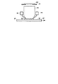
所定基板上に、第1の反射防止膜層を形成する。前記第1の反射防止層は、基板の加工マスクとなる材料である。第1の反射防止膜層上に、第2の反射防止膜層を形成する。第2の反射防止膜は、前記第1の反射防止膜の加工マスクとなる材料である。第2のマスク材料上に、レジスト膜用塗布溶液を供給して回転塗布により化学増幅型レジスト膜形成用塗布溶液を塗布する。所定温度および時間による塗布後ベークによって、化学増幅型レジスト膜を形成する。基板を露光光が157nmの液浸露光装置に搬送する。液浸露光装置内には、あるレイヤーの半導体素子パターンを形成するためのフォトマスクが格納されている。液浸露光装置の構成を図1に示す。図1は、本発明の第1の実施形態に係わる露光装置の概略構成を示す図である。図示されない照明光学系の下方にレチクルステージ31が配置されている。レチクルステージ31上にフォトマスクであるレチクル32が設置されている。レチクルステージ31は平行移動可能である。レチクルステージ31の下方に投影レンズ系33が配置されている。投影レンズ系33の下方にウェハステージ34が配置されている。ウェハステージ34上に前述した処理が行われた半導体基板10が設置されている。ウェハステージ34は、半導体基板10と共に平行移動する。半導体基板10の周囲にはサポート板37が設けられている。
A first antireflection film layer is formed on a predetermined substrate. The first antireflection layer is a material that serves as a processing mask for the substrate. A second antireflection film layer is formed on the first antireflection film layer. The second antireflection film is a material that serves as a processing mask for the first antireflection film. A resist film coating solution is supplied onto the second mask material, and a chemically amplified resist film forming coating solution is applied by spin coating. A chemically amplified resist film is formed by baking after coating at a predetermined temperature and time. The substrate is transported to an immersion exposure apparatus with exposure light of 157 nm. A photomask for forming a semiconductor element pattern of a layer is stored in the immersion exposure apparatus. The configuration of the immersion exposure apparatus is shown in FIG. FIG. 1 is a view showing the schematic arrangement of an exposure apparatus according to the first embodiment of the present invention. A
投影レンズ系33の下方には、フェンス35が取り付けられている。投影レンズ系33の横にフェンス35内への溶液の供給及びフェンス35内からの水の排出を行う一対の溶液供給・排出器36が設けられている。露光は、フェンス35と投影レンズ33で囲まれた領域の基板10と投影レンズ系33との間に溶液が介在した状態で行われる。照射領域にあたる基板表面のフォトレジストにレチクル32上のマスクパターン(図示せず)の像が投影され、潜像が形成される。
A
図1に示した液浸露光装置により、レチクル上のパターンを化学増幅型レジスト膜に転写する。本実施形態では、投影レンズ系と基板との間に介在する溶液として、フッ素溶剤に所定濃度の酸を添加したものを用いる。フッ素溶剤は、気体を含む溶存物を除去した工業的に可能な純粋な溶液である。 The pattern on the reticle is transferred to the chemically amplified resist film by the immersion exposure apparatus shown in FIG. In this embodiment, a solution obtained by adding a predetermined concentration of acid to a fluorine solvent is used as a solution interposed between the projection lens system and the substrate. The fluorine solvent is an industrially possible pure solution from which dissolved substances including gas are removed.
前記露光工程後の基板に対して、所定時間温度のPEB工程を行う。2.38%のTMAH現像液による所定時間の現像を行う。現像リンス工程を行った後、乾燥工程を行う。現像リンス工程は典型的には純水で行うが、界面活性剤の添加や、極性溶媒による置換、超臨界状態の気体による置換などを実施してもよい。 A PEB process at a temperature for a predetermined time is performed on the substrate after the exposure process. 2. Develop for a predetermined time with 38% TMAH developer. After performing the development rinsing step, the drying step is performed. The development rinsing step is typically performed with pure water. However, addition of a surfactant, substitution with a polar solvent, substitution with a gas in a supercritical state, or the like may be performed.
酸が添加された溶液を用いると、酸を添加しない場合に比べて、レジストパターンのT−top形状の改善、またウェハ面内及び/或いはショット面内におけるレジストパターン寸法・形状の均一性が改善される。また、レジストの現像欠陥の低減が期待できる場合がある。 Using an acid-added solution improves the T-top shape of the resist pattern and improves the uniformity of the resist pattern size and shape in the wafer surface and / or in the shot surface, compared to when no acid is added. Is done. In some cases, development defects of the resist can be expected to be reduced.
T−top形状の改善効果は下記要因に因ると考えられる。 The improvement effect of the T-top shape is considered to be due to the following factors.
要因1:レジスト膜中から溶液に溶出した塩基物質が、レジスト表面に吸着し、結果的に露光部の光発生酸が不足する場合。この場合には、レジスト膜中から溶出する塩基物質を溶液中の酸がトラップする作用によって改善される。 Factor 1: When the basic substance eluted into the solution from the resist film is adsorbed on the resist surface, resulting in a shortage of photogenerated acid in the exposed area. In this case, the basic substance eluted from the resist film is improved by the action of the acid in the solution trapping.
要因2:レジスト膜中の光酸発生剤(PAG:Photo Acid Generator)が溶液へ溶出し、レジスト膜露光部におけるPAGの不足によって光発生酸が不足する場合。この場合には、レジスト露光部において不足する酸を溶液中の酸が補う作用によって改善される。 Factor 2: A photoacid generator (PAG) in the resist film is eluted into the solution, and the photogenerated acid is insufficient due to the lack of PAG in the exposed portion of the resist film. In this case, it is improved by the action of the acid in the solution supplementing the acid deficient in the resist exposure part.
要因3:レジスト膜中の露光部の光発生酸が溶液に溶出し、レジスト膜露光部の酸が不足する場合。この場合には、要因2と同様にレジスト露光部において不足する酸を溶液中の酸が補う作用とともに、特にレジスト膜露光部中からの酸の溶液への溶出を概同種の物質が存在することで溶出速度を低下させる作用によって改善される。 Factor 3: The photogenerated acid in the exposed portion of the resist film is eluted into the solution, and the acid in the exposed portion of the resist film is insufficient. In this case, as in Factor 2, the acid in the solution compensates for the acid deficient in the resist exposure area, and in particular, there is a substance of almost the same type that dissolves the acid from the resist film exposure area into the solution. This is improved by the action of lowering the dissolution rate.
要因4:レジスト膜に浸透した溶液が乾燥することで、レジスト膜表面にレジスト膜中の物質が偏析、あるいは膜厚方向の分布の変化を生じて、レジスト膜表面の疎水性が増加する場合。より詳細には、レジスト膜の表面状態の差によって、露光後にレジスト表面に吸着あるいは浸入する光路溶液量が変化するためにPEB工程の基板温度がウェハ面内で変化し、パターン寸法・形状に影響する。また、現像工程における現像液のレジスト中への浸入速度に差が生じる。この場合には、レジスト膜上の酸濃度を高めることで溶解抑止基の脱離反応を促進し、親水化する作用によって改善される。 Factor 4: When the solution infiltrated into the resist film is dried, substances in the resist film are segregated on the resist film surface or the distribution in the film thickness direction is changed, thereby increasing the hydrophobicity of the resist film surface. More specifically, the substrate temperature in the PEB process changes within the wafer surface due to the difference in the surface condition of the resist film, so that the amount of the optical path solution adsorbed or infiltrated into the resist surface after exposure changes within the wafer surface. To do. In addition, a difference occurs in the penetration speed of the developer into the resist in the development process. In this case, by increasing the acid concentration on the resist film, the elimination reaction of the dissolution inhibiting group is promoted to improve the hydrophilicity.
また、光路周辺のみに局所的な領域に溶液を供給する液浸露光装置においては、ショット配置および露光順序などによって、溶液とレジスト膜との接触履歴に差が生じる。その結果、要因1〜4の要因について、前記接触履歴に応じて差が出ることから、ウェハ面内及び/或いはショット内においてレジストパターン寸法・形状に差が生じると考えられる。溶液に酸を入れることによって、T−top形状の緩和と同時にパターン寸法・形状の均一性改善効果を得ることが可能となる。 Further, in an immersion exposure apparatus that supplies a solution to a local region only around the optical path, a difference occurs in the contact history between the solution and the resist film depending on the shot arrangement and the exposure order. As a result, the factors 1 to 4 differ depending on the contact history, so that it is considered that there is a difference in the resist pattern size and shape within the wafer surface and / or within the shot. By adding an acid to the solution, it becomes possible to obtain the effect of improving the uniformity of the pattern size and shape simultaneously with the relaxation of the T-top shape.
溶液に添加する酸の種類としては、硫酸、硝酸、亜硝酸、酢酸、塩酸、次亜塩素酸、パーフロロアルキルスルホン酸やシクロヘキシルスルホン酸などの有機スルホン酸などの有機スルホン酸などの種々の酸が考えられる。化学増幅型レジストに使用される光酸発生剤から光反応によって発生する酸の典型例は、有機スルホン酸である。より詳細には、要因1〜4のレジスト形状不良の原因によって望ましい酸の種類が変化すると考えられる。 Acids added to the solution include various acids such as sulfuric acid, nitric acid, nitrous acid, acetic acid, hydrochloric acid, hypochlorous acid, organic sulfonic acids such as organic sulfonic acids such as perfluoroalkyl sulfonic acid and cyclohexyl sulfonic acid. Can be considered. A typical example of an acid generated by a photoreaction from a photoacid generator used in a chemically amplified resist is an organic sulfonic acid. More specifically, it is considered that the desired acid type varies depending on the cause of the resist shape defect of factors 1 to 4.
要因1においては、塩基物質のトラップが重要であることから、一般論としては生成される塩の乖離定数が低い弱酸が望ましい。 In factor 1, trapping of the basic substance is important, and therefore, as a general rule, a weak acid having a low dissociation constant of the generated salt is desirable.
要因2〜要因4においては、レジスト膜中に含まれる光酸発生剤が露光して発生する光発生酸と同じ酸であることがもっとも望ましい。これは、PEB工程における脱保護反応に対する寄与、さらに拡散特性が変化しないために、レジストパターン寸法・形状の均一性を改善する効果が高いためである。あるいは、PEB工程におけるレジストの脱保護反応が拡散律速反応、反応律速反応であるに応じて、反応の律速要因である特性が元の光発生酸と概等しい酸を光路媒質中に添加することが、レジストパターン形状・寸法均一性改善の上で望ましい。前述したように、光酸発生剤から光反応によって発生する酸の典型例は、有機スルホン酸である。パーフロロアルキルスルホン酸の例としては、トリフロロメチルスルホン酸、ノナフロロブチルスルホン酸、がある。 In factors 2 to 4, it is most desirable that the photoacid generator contained in the resist film is the same acid as the photogenerated acid generated by exposure. This is because the contribution to the deprotection reaction in the PEB process and the diffusion characteristics do not change, and the effect of improving the uniformity of resist pattern dimensions and shapes is high. Alternatively, depending on whether the resist deprotection reaction in the PEB process is a diffusion-controlled reaction or a reaction-controlled reaction, an acid whose characteristics that are the rate-limiting factor of the reaction are approximately the same as the original photogenerated acid may be added to the optical path medium. It is desirable for improving the resist pattern shape and dimensional uniformity. As described above, a typical example of an acid generated by a photoreaction from a photoacid generator is an organic sulfonic acid. Examples of perfluoroalkylsulfonic acid include trifluoromethylsulfonic acid and nonafluorobutylsulfonic acid.
前記いずれの要因であっても、液浸露光工程における光路媒質とレジスト膜の接触に起因してレジスト表面に形成される表面難溶層が緩和される。その結果、溶解不良に起因する現像欠陥の低減が期待できる。 Regardless of the above factors, the hardly soluble surface layer formed on the resist surface due to the contact between the optical path medium and the resist film in the immersion exposure process is relaxed. As a result, a reduction in development defects due to poor dissolution can be expected.
酸の濃度としては、レジストパターンに対する前記効果が得られるに十分である、出来るだけ低濃度で使用することが望ましい。これは、一つには光路媒質の屈折率の変化に伴う投影光学系の調整を必要としないことが望ましいこと、さらには露光装置の光路媒質と接触する機構の腐食等の可能性を出来るだけ低減するためである。 It is desirable that the acid concentration be as low as possible, which is sufficient to obtain the above effect on the resist pattern. For one thing, it is desirable not to require adjustment of the projection optical system in accordance with the change in the refractive index of the optical path medium. Furthermore, the possibility of corrosion of the mechanism that contacts the optical path medium of the exposure apparatus is as much as possible. This is to reduce.
本実施形態では157nm用液浸露光を想定して記述したが、純水以外の光路媒質を使用する液浸露光であれば、光源の波長が異なっても同様の効果を得られる場合がある。 In the present embodiment, description has been made on the assumption that immersion exposure for 157 nm is used. However, in the case of immersion exposure using an optical path medium other than pure water, the same effect may be obtained even if the wavelength of the light source is different.
レジスト膜上に保護膜を使用した場合であっても、保護膜の溶液に対する遮蔽性が完全ではない場合、保護膜の塗布溶媒によって溶解したレジスト膜中成分の保護膜中への取り込みが起きる場合、保護膜塗布及び/或いは加熱における表面への吸着物の付着が生じる場合、においては前記と同様の効果が得られる。 Even when a protective film is used on the resist film, if the protective film is not completely shielded from the solution, the components in the resist film dissolved by the coating solvent of the protective film may be taken into the protective film. In the case where the adsorbate adheres to the surface by applying the protective film and / or heating, the same effect as described above can be obtained.
この場合、レジスト膜上への保護膜用塗布溶液の塗布工程および加熱工程が、レジスト膜形成構成とパターン露光工程の間に加わり、PEB工程の後に保護膜の剥離工程が追加される。保護膜の剥離工程としては、専用の剥離溶剤を用いた保護膜剥離工程と保護膜リンス工程を必要とする場合、あるいはレジスト現像液によって現像工程と連続あるいは保護膜除去リンス工程をさらに追加する場合がある。 In this case, a coating process and a heating process of the protective film coating solution on the resist film are added between the resist film forming configuration and the pattern exposure process, and a protective film peeling process is added after the PEB process. When the protective film peeling process requires a protective film peeling process and a protective film rinsing process using a special peeling solvent, or when a development process and a continuous or protective film removal rinsing process are further added by a resist developer There is.
いずれの種類の保護膜の場合であっても、本実施形態において、レジスト膜表面とある記載を保護膜表面と読み替える。 Regardless of the type of protective film, in this embodiment, the description of the resist film surface is read as the protective film surface.
(第2の実施形態)
純水以外の光路媒質を用いる液浸露光装置を用いる場合において、前記光路媒質に酸を添加する場合の実施形態について記述する。
(Second Embodiment)
An embodiment in which an acid is added to the optical path medium when an immersion exposure apparatus using an optical path medium other than pure water is used will be described.
本実施形態では、レジスト膜上に保護膜が形成された場合について説明する。 In this embodiment, a case where a protective film is formed on a resist film will be described.
ウェハ上に第1の実施形態と同様に化学増幅型レジスト膜を形成する。さらに、化学増幅型レジスト膜上に保護膜用塗布溶液を塗布する。必要に応じて所定時間・温度の加熱を行うことで、化学増幅型レジスト膜上に保護膜を形成する。保護膜形成後、液浸露光を行う。液浸露光の条件は、第1の実施形態と同様に、露光波長が157nm、液浸溶液が酸を添加したフッ素溶剤である。 A chemically amplified resist film is formed on the wafer as in the first embodiment. Further, a protective film coating solution is applied on the chemically amplified resist film. A protective film is formed on the chemically amplified resist film by heating for a predetermined time and temperature as necessary. After forming the protective film, immersion exposure is performed. The conditions for immersion exposure are, as in the first embodiment, an exposure wavelength of 157 nm and the immersion solution is a fluorine solvent to which an acid is added.
露光後の基板に対して、所定時間温度のPEB工程を行う。保護膜上に所定の保護膜剥離液を供給して保護膜を剥離する。剥離後、純水による剥離後リンス処理を行う。典型的には2.38%のTMAH現像液により所定時間現像して、レジストパターンを形成する。現像後リンス処理を行った後、乾燥処理を行う。剥離後リンス処理、現像後リンス処理は純水で行うが、界面活性剤の添加や、極性溶媒による置換、超臨界状態の気体による置換などを実施してもよい。 A PEB process at a temperature for a predetermined time is performed on the exposed substrate. A predetermined protective film stripping solution is supplied onto the protective film to peel the protective film. After peeling, a rinsing process after peeling with pure water is performed. Typically, a resist pattern is formed by developing with a 2.38% TMAH developer for a predetermined time. After the development, a rinsing process is performed, followed by a drying process. The post-peeling rinse treatment and post-development rinse treatment are performed with pure water, but addition of a surfactant, substitution with a polar solvent, substitution with a gas in a supercritical state, or the like may be performed.
なお、本実施形態においては、専用の保護膜剥離剤を使用する場合を記述したが、現像液で溶解する保護膜を使用して、保護膜除去と現像とを連続的に行ってもよい。あるいは、現像液に溶解する保護膜であっても、保護膜の現像液への必要溶解時間などにおいて一度現像液及び保護膜の溶解物を除去し、必要に応じてリンス工程を行った後に、再び現像液の供給を行ってもよい。 In the present embodiment, the case where a dedicated protective film remover is used has been described. However, the protective film may be removed and developed continuously using a protective film that dissolves in a developer. Alternatively, even if the protective film dissolves in the developer, after removing the developer and protective film dissolved once in the required dissolution time of the protective film in the developer, etc., after performing a rinse step as necessary, You may supply a developing solution again.
液浸溶液に酸を添加したフッ素溶液を用いることによって、前記酸を添加しない場合に比べて、レジストパターンのT−top形状の改善、またウェハ面内及び/或いはショット面内におけるレジストパターン寸法・形状の均一性が改善される。また、保護膜の剥離不良が改善されることも考えられる。 By using a fluorine solution in which an acid is added to the immersion solution, the T-top shape of the resist pattern is improved as compared with the case where the acid is not added, and the resist pattern dimensions in the wafer surface and / or the shot surface are Shape uniformity is improved. It is also conceivable that the defective peeling of the protective film is improved.
保護膜を使用する場合には、保護膜の基本特性である光路媒質の遮蔽性よびレジスト膜中組成物の溶出の遮蔽性の程度によって、前記効果が得られる要因がある程度異なると考えられる。 In the case of using a protective film, it is considered that the factors for obtaining the effect differ to some extent depending on the shielding property of the optical path medium and the shielding property of elution of the composition in the resist film, which are basic characteristics of the protective film.
保護膜の前記2つの遮蔽性が不十分である場合には、程度の差はあるものの、第1の実施形態に記載した保護膜を使用しない場合と概同一の要因が存在する。特に、第1の実施形態に記載の要因1〜3については、望ましい酸の種類も同一である。 When the two shielding properties of the protective film are insufficient, although there is a difference in degree, there are almost the same factors as when the protective film described in the first embodiment is not used. In particular, for the factors 1 to 3 described in the first embodiment, the types of desirable acids are the same.
第1の実施形態に記載の要因4は、保護膜を使用する本実施形態においては重要ではない。一方で、保護膜表面の乾燥状態が、保護膜と光路媒質との接触履歴によって変化する。その結果、第1の実施形態に記載の要因4と同様にPEBの温度履歴の差が生じて、パターン寸法・形状均一性に影響すると考えられるため、同様に酸を添加して保護膜の表面状態を均一にするで、パターン寸法・形状均一性が改善される。 The factor 4 described in the first embodiment is not important in the present embodiment using the protective film. On the other hand, the dry state of the protective film surface changes depending on the contact history between the protective film and the optical path medium. As a result, it is considered that a difference in temperature history of PEB occurs similarly to the factor 4 described in the first embodiment, and this affects the pattern dimension / shape uniformity. By making the state uniform, pattern dimension / shape uniformity is improved.
一方、保護膜の前記2つの遮蔽性が十分優れている場合には、主に保護膜表面状態が保護膜と光路媒質との接触履歴の差によって変化することによる光路媒質の吸着量に差が生じてPEB温度履歴に差が生じることに由来すると考えられる。 On the other hand, when the two shielding properties of the protective film are sufficiently excellent, there is a difference in the adsorption amount of the optical path medium mainly due to a change in the surface state of the protective film due to a difference in contact history between the protective film and the optical path medium. This is considered to be derived from the difference in PEB temperature history.
保護膜中には低分子成分が存在していなくとも、保護膜用塗布溶液のレジスト上への供給時において、レジスト膜、特にその上部に偏析している光酸発生剤が保護膜中に取り込まれ、保護膜上部に偏析する。前記保護膜中の偏析物の分布が前記接触履歴によって変化することでレジスト表面状態が変化すると考えられる。これに対して、保護膜表面に酸を供給することで、表面状態の変化を緩和できると考えられる。 Even when low molecular components are not present in the protective film, the resist film, especially the photoacid generator segregated on the upper part, is taken into the protective film when supplying the coating solution for the protective film onto the resist. And segregates on top of the protective film. It is considered that the resist surface state changes when the distribution of segregated substances in the protective film changes according to the contact history. On the other hand, it is thought that the change of the surface state can be alleviated by supplying an acid to the surface of the protective film.
光路媒質への酸の添加量としては、レジストパターンに対する前記効果が得られるに十分である、出来るだけ低濃度で使用することが望ましい。これは、一つには光路媒質の屈折率の変化に伴う投影光学系の調整を必要としないことが望ましいこと、さらには露光装置の光路媒質と接触する機構の腐食等の可能性を出来るだけ低減するためである。 As for the amount of acid added to the optical path medium, it is desirable to use it at a concentration as low as possible, which is sufficient to obtain the above effect on the resist pattern. For one thing, it is desirable not to require adjustment of the projection optical system in accordance with the change in the refractive index of the optical path medium. Furthermore, the possibility of corrosion of the mechanism that contacts the optical path medium of the exposure apparatus is as much as possible. This is to reduce.
本実施形態は157nm用液浸露光を想定して記述したが、純水以外の光路媒質を使用する液浸露光であれば、光源の波長が異なっても同様の効果が得られる場合がある。 Although this embodiment has been described on the assumption that immersion exposure for 157 nm is used, if immersion exposure using an optical path medium other than pure water is used, the same effect may be obtained even if the wavelength of the light source is different.
(第3の実施形態)
第1の実施形態では、純水以外の溶媒に酸を添加した光路媒質を用いて液浸露光を行う方法を説明した。本実施形態では、純水以外の溶媒に界面活性剤を添加して液浸露光を行う方法について説明する。本実施形態では、保護膜を使用しない場合の実施形態について記述する。界面活性剤が添加された光路媒質を用いて液浸露光を行うこと以外は、第1の実施形態と同様なのでレジスト膜形成から現像までの工程の詳しい説明を省略する。
(Third embodiment)
In the first embodiment, the method of performing immersion exposure using an optical path medium in which an acid is added to a solvent other than pure water has been described. In this embodiment, a method for performing immersion exposure by adding a surfactant to a solvent other than pure water will be described. In this embodiment, an embodiment in which a protective film is not used will be described. Except for performing immersion exposure using an optical path medium to which a surfactant is added, the process is the same as in the first embodiment, so detailed description of the steps from resist film formation to development is omitted.
界面活性剤が添加された光路媒質を用いることで、光路媒質中の泡の発生量あるいは大きさが変化し、光学像の劣化、異常パターンの転写を低減できる。 By using an optical path medium to which a surfactant is added, the amount or size of bubbles generated in the optical path medium changes, and optical image degradation and abnormal pattern transfer can be reduced.
レジスト表面状態は、光路媒質とレジストとの接触履歴の差によって変化すると考えられる。また、光路媒質の吸着量あるいは浸入量の変化によって生じるPEB工程の温度履歴の変動によって、ウェハ面内/ショット面内におけるレジストパターン寸法・形状の不均一性が生じる。レジスト表面状態を界面活性剤の作用によって均一にすることで、前記寸法・形状の均一性が向上すると考えられる。 The resist surface state is considered to change depending on the difference in contact history between the optical path medium and the resist. In addition, variations in the temperature history of the PEB process caused by changes in the adsorption amount or penetration amount of the optical path medium cause non-uniformity of resist pattern dimensions and shapes in the wafer surface / shot surface. It is considered that the uniformity of the size and shape is improved by making the resist surface state uniform by the action of the surfactant.
界面活性剤が添加された光路媒質を用いる方法は、光路媒質中への溶出による光発生酸あるいはPAGの不足もしくは光路媒質中に溶出した塩基のレジスト表面への付着によるレジスト表面の溶解抑止基脱離反応の不足による表面難溶層の形成、光路媒質の乾燥によるレジスト表面の疎水化、などに起因するレジストパターンのT−top形状や形状の差異、現像欠陥の発生などに対して、レジスト膜表面を親水化させることで改善させると考えられる。 In the method using the optical path medium to which the surfactant is added, the dissolution inhibiting group is removed from the resist surface due to lack of photogenerated acid or PAG due to elution into the optical path medium or adhesion of the base eluted into the optical path medium to the resist surface. Resist film against resist pattern T-top shape and shape difference, development defect, etc. due to formation of poorly soluble layer due to insufficient separation reaction, hydrophobicity of resist surface by drying optical path medium, etc. It can be improved by making the surface hydrophilic.
本実施形態は157nm用液浸露光を想定して記述したが、純水以外の光路媒質を使用する液浸露光であれば、光源の波長が異なっても同様の効果を得られる場合がある。 Although this embodiment has been described on the assumption that immersion exposure for 157 nm is used, if immersion exposure uses an optical path medium other than pure water, the same effect may be obtained even if the wavelength of the light source is different.
本実施形態では、レジスト膜上に保護膜を使用しない場合について記述した。しかし、本実施形態は保護膜を使用する場合であっても、保護膜の前記遮蔽性に問題がある場合にはレジスト膜とほぼ同様に、前記遮蔽性が十分であっても保護膜用塗布溶液供給時に取り込まれる成分のために、ウェハ面内において基板表面状態に差が生じる。したがって、保護膜を使用する場合であっても、光路媒質に溶解して不足する酸を補充する効効果によって、ウェハ面内における基板表面状態の差を改善することが可能となる。 In this embodiment, the case where no protective film is used on the resist film has been described. However, even if a protective film is used in this embodiment, if there is a problem with the shielding property of the protective film, the coating for the protective film can be applied even if the shielding property is sufficient, almost like the resist film. Due to the components taken in when the solution is supplied, a difference occurs in the substrate surface state in the wafer surface. Therefore, even when a protective film is used, it is possible to improve the difference in the substrate surface state in the wafer plane due to the effect of replenishing the acid that is dissolved and deficient in the optical path medium.
(第4の実施形態)
本実施形態では、露光波長が193nmの液浸露光装置を用いて露光を行う例を説明する。
(Fourth embodiment)
In this embodiment, an example in which exposure is performed using an immersion exposure apparatus having an exposure wavelength of 193 nm will be described.
ウェハ上に、必要に応じて反射防止膜を形成する。反射防止膜上に化学増幅型レジスト膜用塗布溶液を塗布する。塗布後ベーク(Pre Bake)を行って化学増幅型レジスト膜を形成する。少なくとも投影レンズ系の対物レンズから発した光が前記基板に達する光のパスが光路媒質で満たされた液浸露光装置を用いて、前記基板上の化学増幅型レジスト膜に対して、所定のフォトマスクに形成されたパターンを転写する。 An antireflection film is formed on the wafer as necessary. A coating solution for chemically amplified resist film is applied on the antireflection film. After application, baking is carried out (Pre Bake) to form a chemically amplified resist film. At least a predetermined photo is applied to the chemically amplified resist film on the substrate using an immersion exposure apparatus in which a light path from which at least the light emitted from the objective lens of the projection lens system reaches the substrate is filled with an optical path medium. The pattern formed on the mask is transferred.
本実施形態では、純水に塩を添加した緩衝溶液が光路媒質として用いられる。塩の濃度は、光学定数の変化が露光装置の解像性に実質的に影響しない程度に調整される。パターンが転写された化学増幅型レジスト膜に対して、PEB工程、2.38%のTMAHによる現像工程、純水によるリンス工程を順次行う。緩衝溶液とは、化学反応の結果生ずる水素イオン濃度の変化を,最小にするように調製された溶液のことである。 In this embodiment, a buffer solution obtained by adding a salt to pure water is used as the optical path medium. The concentration of the salt is adjusted to such an extent that the change in the optical constant does not substantially affect the resolution of the exposure apparatus. A PEB process, a development process using 2.38% TMAH, and a rinsing process using pure water are sequentially performed on the chemically amplified resist film to which the pattern has been transferred. A buffer solution is a solution prepared to minimize the change in hydrogen ion concentration resulting from a chemical reaction.
緩衝溶液を用いると、純水の場合に比べて、レジストパターン形状のウェハ/ショット内の位置による差が緩和する。 When the buffer solution is used, the difference due to the position of the resist pattern shape in the wafer / shot is reduced as compared with the case of pure water.
緩衝溶液を光路媒質とする方法は、光路媒質が純水の場合におけるT−top形状のウェハ/ショット内位置による差が緩和することの原因が、下記の場合において有効であると考えられる。 The method using the buffer solution as the optical path medium is considered to be effective in the following cases because the difference due to the T-top shaped wafer / shot position when the optical path medium is pure water is relaxed.
要因I:レジスト膜中から光路媒質に溶出した光発生酸がレジスト表面に吸着し、光発生酸のレジスト表面への吸着量がウェハ/ショット内位置によって差異が存在し、レジスト膜形状に差異が発生する場合。 Factor I: The photogenerated acid eluted from the resist film into the optical path medium is adsorbed on the resist surface, and the amount of photogenerated acid adsorbed on the resist surface varies depending on the position in the wafer / shot, and the resist film shape varies. If it occurs.
要因II:この場合には、レジスト膜中から溶出する光発生酸を光路媒質中の塩基がトラップし、付着量を一定とする作用による。 Factor II: In this case, the photogenerated acid eluted from the resist film is trapped by the base in the optical path medium, and the adhesion amount is made constant.
要因III:レジスト膜中のPAGが光路媒質に溶出し、光路媒質中において発生する光発生酸のレジスト表面への吸着量がウェハ/ショット内位置によって差異が存在し、レジスト膜形状に差異が発生する場合。 Factor III: PAG in the resist film elutes into the optical path medium, and the amount of photogenerated acid adsorbed on the resist surface in the optical path medium varies depending on the position within the wafer / shot, resulting in differences in resist film shape If you want to.
要因IV:この場合には、レジスト膜中から溶出する光発生酸を光路媒質中の塩基がトラップし、付着量を一定とする作用による。 Factor IV: In this case, the photogenerated acid eluted from the resist film is trapped by the base in the optical path medium, and the adhesion amount is made constant.
要因V:ウェハ上のパターンレイアウトに依存して光路媒質中に溶出する光発生酸の量が変化することで、パターンレイアウトによって収差量が変化し、その影響によってレジストパターン寸法・形状が変化する。この作用が溶解した物質濃度に応じて変化する光路媒質の屈折率の変化が、緩衝作用によって緩和され、レイアウトに依存したレジストパターン寸法・形状変化が緩和される。ただし、この影響自体は比較的小さいものであると考えられる。 Factor V: The amount of photogenerated acid that elutes into the optical path medium changes depending on the pattern layout on the wafer, so that the amount of aberration changes depending on the pattern layout, and the resist pattern size and shape change due to the influence. The change in the refractive index of the optical path medium, which changes according to the dissolved substance concentration, is alleviated by the buffering action, and the resist pattern size / shape change depending on the layout is alleviated. However, this effect itself is considered to be relatively small.
緩衝溶液としては、種々の弱酸あるいは中酸と弱塩基あるいは中塩基との塩が望ましい。さらに、緩衝溶液が酸性側の組成であることが望ましい。また、レジスト表面への付着が少ない塩の塩基アニオンあるいは塩基を添加されていることが望ましい。 As the buffer solution, salts of various weak acids or intermediate acids and weak bases or intermediate bases are desirable. Furthermore, it is desirable that the buffer solution has an acidic composition. Further, it is desirable to add a salt base anion or a base which hardly adheres to the resist surface.
レジスト膜上に保護膜を形成した場合であっても、保護膜の光路媒質に対する遮蔽性が完全ではない場合、保護膜の塗布溶媒によって溶解したレジスト膜中成分の保護膜中への取り込みが起きる場合、保護膜塗布及び/或いは加熱における表面への吸着物の付着が生じる場合、においては前記と同様の効果が得られる。 Even when the protective film is formed on the resist film, if the protective film is not completely shielded against the optical path medium, the components in the resist film dissolved by the coating solvent of the protective film are taken into the protective film. In this case, when the adsorbate adheres to the surface by applying the protective film and / or heating, the same effect as described above can be obtained.
この場合、レジスト膜上への保護膜用塗布溶液の塗布工程および加熱工程が、レジスト膜形成構成とパターン露光工程の間に加わり、PEB工程の後に保護膜の剥離工程が追加される。保護膜の剥離工程としては、専用の剥離溶剤を用いた保護膜剥離工程と保護膜リンス工程を必要とする場合、あるいはレジスト現像液によって現像工程と連続あるいは保護膜除去リンス工程をさらに追加する場合がある。いずれの種類の保護膜の場合であっても、本実施形態において、レジスト膜表面とある記載を保護膜表面と読み替える。 In this case, a coating process and a heating process of the protective film coating solution on the resist film are added between the resist film forming configuration and the pattern exposure process, and a protective film peeling process is added after the PEB process. When the protective film peeling process requires a protective film peeling process and a protective film rinsing process using a special peeling solvent, or when a development process and a continuous or protective film removal rinsing process are further added by a resist developer There is. Regardless of the type of protective film, in this embodiment, the description of the resist film surface is read as the protective film surface.
(第5の実施形態)
第5の実施形態では、純水に酸化性物質を添加した溶液を用いて液浸露光を行う。酸化性物質の種類としては、過酸化水素水、オゾン、次亜塩素酸、酸素などが考えられる。酸化性物質の濃度は、純水からの光学定数の変化が露光装置の解像性に実質的に影響しない範囲にすることが好ましい。光路媒質が異なること以外は、第3の実施形態と同様なのでレジストパターンの形成についての詳細な説明を省略する。
(Fifth embodiment)
In the fifth embodiment, immersion exposure is performed using a solution obtained by adding an oxidizing substance to pure water. As the kind of the oxidizing substance, hydrogen peroxide water, ozone, hypochlorous acid, oxygen and the like can be considered. The concentration of the oxidizing substance is preferably in a range where the change in optical constant from pure water does not substantially affect the resolution of the exposure apparatus. Except that the optical path medium is different, the third embodiment is the same as the third embodiment, and thus detailed description of the formation of the resist pattern is omitted.
酸化性物質が添加されている光路媒質を用いることによって、得られるレジストパターンのT−top形状が緩和し、あるいは/およびエッジラフネスの低下/周辺パターン密度に依存した着目パターン寸法変化の低下、が期待できる。また、レジスト表面の表面難溶層の除去作用、レジスト表面の親水化作用を有することによって、T−top形状の緩和、それに由来するエッジラフネスの低下、現像欠陥の減少、などの効果が得られると考えられる。 By using an optical path medium to which an oxidizing substance is added, the T-top shape of the obtained resist pattern is relaxed, or / and the edge roughness is reduced / the pattern size change of interest depending on the peripheral pattern density is reduced. I can expect. Further, by having the action of removing the hardly soluble layer on the resist surface and the action of hydrophilizing the resist surface, effects such as relaxation of the T-top shape, reduction of edge roughness resulting therefrom, and reduction of development defects can be obtained. it is conceivable that.
レジスト膜上に保護膜を使用した場合であっても、保護膜の光路媒質に対する遮蔽性が完全ではない場合、保護膜の塗布溶媒によって溶解したレジスト膜中成分の保護膜中への取り込みが起きる場合、保護膜塗布及び/或いは加熱における表面への吸着物の付着が生じる場合、においては前記と同様の効果が得られる。 Even when a protective film is used on the resist film, if the protective film is not completely shielded against the optical path medium, the components in the resist film dissolved by the coating solvent of the protective film are taken into the protective film. In this case, when the adsorbate adheres to the surface by applying the protective film and / or heating, the same effect as described above can be obtained.
この場合、レジスト膜上への保護膜用塗布溶液の塗布工程および加熱工程が、レジスト膜形成構成とパターン露光工程の間に加わり、PEB工程の後に保護膜の剥離工程が追加される。保護膜の剥離工程としては、専用の剥離溶剤を用いた保護膜剥離工程と保護膜リンス工程を必要とする場合、あるいはレジスト現像液によって現像工程と連続あるいは保護膜除去リンス工程をさらに追加する場合がある。いずれの種類の保護膜の場合であっても、本実施形態において、レジスト膜表面とある記載を保護膜表面と読み替える。 In this case, a coating process and a heating process of the protective film coating solution on the resist film are added between the resist film forming configuration and the pattern exposure process, and a protective film peeling process is added after the PEB process. When the protective film peeling process requires a protective film peeling process and a protective film rinsing process using a special peeling solvent, or when a development process and a continuous or protective film removal rinsing process are further added by a resist developer There is. Regardless of the type of protective film, in this embodiment, the description of the resist film surface is read as the protective film surface.
(第6の実施形態)
酸化性物質と界面活性剤とが添加された光路媒質を用いることで、基本的特性として、酸化性物質のみ或いは界面活性剤のみを添加した場合と同一の効果が得られる。
(Sixth embodiment)
By using an optical path medium to which an oxidizing substance and a surfactant are added, the same effect as when only an oxidizing substance or only a surfactant is added can be obtained as a basic characteristic.
本実施形態は、第2の実施形態と同様に、化学増幅型レジスト膜上に保護膜が形成された状態で波長157nmの露光光で液浸露光を行う。液浸露光以外の工程は、第2の実施形態と同様なので説明を省略する。 In the present embodiment, as in the second embodiment, immersion exposure is performed with exposure light having a wavelength of 157 nm in a state where a protective film is formed on the chemically amplified resist film. Since the steps other than the immersion exposure are the same as those in the second embodiment, the description thereof is omitted.
添加した酸化性物質の濃度が高い場合には、露光中に泡が発生し、フレアや異常パターン転写の原因となる。このため、酸化性物質の添加によってレジスト膜塗布・レジスト表面状態の親水性の向上を図るにおいても、その上限が存在する。しかるに、酸化性物質、基板膜種に応じた適切な界面活性剤を用いることで、泡の発生を抑制し、より高い親水性の向上作用を得ることが可能となる。その結果、レジストパターン寸法・形状の均一性の向上、表面難溶層の低減による現像欠陥の低減などの効果を得ることが可能となる。 When the concentration of the added oxidizing substance is high, bubbles are generated during exposure, causing flare and abnormal pattern transfer. For this reason, there is an upper limit even when the hydrophilicity of resist film coating and resist surface state is improved by adding an oxidizing substance. However, by using an appropriate surfactant according to the oxidizing substance and the substrate film type, it is possible to suppress the generation of bubbles and obtain a higher hydrophilicity improving effect. As a result, it is possible to obtain effects such as improvement in uniformity of resist pattern dimensions and shape and reduction in development defects due to reduction of the surface insoluble layer.
酸化性物質としては、前記オゾン以外にも、過酸化水素、次亜塩素酸などでも良い。 As the oxidizing substance, hydrogen peroxide, hypochlorous acid or the like may be used in addition to the ozone.
また、純水に変えて、純粋溶媒を使用する液浸露光装置の場合には、さらに付随した効果を得ることが可能となる。157nm用の光路媒質として検討されている下記3溶媒の157nmの吸光係数は、PFPE(perefluorinated polyehers)が6cm-1、PFTG(perfluortriglyime:CF3[OCF2CF2]3OCF3)が0.64cm-1、IF24(デュポン社製)が0.2cm-1である(M. Switkes et al. , J. Vac. Sci. Technol. B21(6), pp. 2794-2799 (2003))。これらの光路媒質の透明性が低い場合には、露光光による光路媒質の分解が生じる。その結果、光路媒質内にガスが発生する。このため、気体あるいは気体を発生させやすい酸化性物質が添加されている場合には、泡が発生する危険性が高い。しかし、適切な界面活性剤を添加することで、泡の発生を抑制することが可能となる。 Further, in the case of an immersion exposure apparatus that uses a pure solvent instead of pure water, an additional effect can be obtained. The extinction coefficient at 157 nm of the following three solvents studied as an optical path medium for 157 nm is 6 cm −1 for PFPE (perefluorinated polyehers) and 0.64 cm for PFTG (perfluortriglyime: CF 3 [OCF 2 CF 2 ] 3 OCF 3 ). -1 and IF24 (manufactured by DuPont) are 0.2 cm -1 (M. Switkes et al., J. Vac. Sci. Technol. B21 (6), pp. 2794-2799 (2003)). When the transparency of these optical path media is low, the optical path medium is decomposed by the exposure light. As a result, gas is generated in the optical path medium. For this reason, when the oxidizing substance which is easy to generate | occur | produce gas or gas is added, the danger that a bubble will generate | occur | produce is high. However, it is possible to suppress the generation of bubbles by adding an appropriate surfactant.
また、本実施形態は、レジスト膜上に保護膜を形成している場合を示したが、保護膜を形成しない場合においても、同様の効果を得ることが可能であって、保護膜の有無による限定されるものではない。 Moreover, although this embodiment showed the case where the protective film was formed on the resist film, even when not forming a protective film, the same effect can be acquired, and it depends on the presence or absence of a protective film. It is not limited.
(第7の実施形態)
本実施形態は、第2の実施形態と同様に、化学増幅型レジスト膜上に保護膜が形成された状態で波長157nmの露光光で液浸露光を行う。液浸露光以外の工程は、第2の実施形態と同様なので説明を省略する。
(Seventh embodiment)
In the present embodiment, as in the second embodiment, immersion exposure is performed with exposure light having a wavelength of 157 nm in a state where a protective film is formed on the chemically amplified resist film. Since the steps other than the immersion exposure are the same as those in the second embodiment, the description thereof is omitted.
本実施形態では、純水以外の溶媒に酸と界面活性剤とが添加された光路媒質を用いる場合について記述する。望ましい酸の種類は第1の実施形態に記載されたものと同様である。酸と界面活性剤とが添加された光路媒質を用いることで、基本的特性として、酸のみを添加した場合と界面活性剤のみを添加した効果を併せた効果が得られる。 In the present embodiment, a case where an optical path medium in which an acid and a surfactant are added to a solvent other than pure water will be described. Desirable acid types are the same as those described in the first embodiment. By using an optical path medium to which an acid and a surfactant are added, an effect that combines the effect of adding only the acid and the effect of adding only the surfactant can be obtained as basic characteristics.
さらに下記の副次的効果を得ることができる。酸の種類によっては、添加した酸の濃度が高い場合には、露光中に泡が発生し、フレアや異常パターン転写の原因となる場合が存在する。このため、酸の添加によってレジスト膜中の酸の不足あるいは塩基の溶出の影響を打ち消す効果を得るにおいても、その添加量の上限から、得られる効果の上限が存在していた。しかるに、添加する酸、基板膜種に応じた適切な界面活性剤を用いることで、泡の発生を抑制し、より高いレジストパターン寸法・形状均一性の改善、現像欠陥改善の効果を得ることが可能となる。 Furthermore, the following secondary effects can be obtained. Depending on the type of acid, when the concentration of the added acid is high, bubbles may be generated during exposure, which may cause flare and abnormal pattern transfer. For this reason, even when the effect of canceling out the effects of acid shortage or base elution in the resist film is obtained by addition of acid, there is an upper limit of the effect obtained from the upper limit of the amount added. However, by using an appropriate surfactant according to the acid to be added and the type of the substrate film, it is possible to suppress the generation of bubbles and to obtain higher resist pattern dimension / shape uniformity improvement and development defect improvement effects. It becomes possible.
また、純水に変えて、純粋溶媒を使用する液浸露光装置の場合には、さらに付随した効果を得ることが可能となる。157nm用の光路媒質として検討されている下記3溶液の157nmの吸光係数は、PFPE(perefluorinated polyehers)が6cm-1、PFTG(perfluortriglyime:CF3[OCF2CF2]3OCF3)が0.64cm-1、IF24(デュポン社製)が0.2cm-1である(M. Switkes et al. , J. Vac. Sci. Technol. B21(6), pp. 2794-2799 (2003))。これらの光路媒質の透明性が低い場合には、露光光による光路媒質の分解が生じる。その結果、光路媒質においてガスが発生する。このため、気体あるいは気体を発生する酸化性物質が添加されている場合には、泡が発生する危険性が高い。しかし、適切な界面活性剤を添加することで、泡の発生を抑制することが可能となる。 Further, in the case of an immersion exposure apparatus that uses a pure solvent instead of pure water, an additional effect can be obtained. The extinction coefficient at 157 nm of the following three solutions studied as an optical path medium for 157 nm is 6 cm −1 for PFPE (perefluorinated polyehers) and 0.64 cm for PFTG (perfluortriglyime: CF 3 [OCF 2 CF 2 ] 3 OCF 3 ). -1 and IF24 (manufactured by DuPont) are 0.2 cm -1 (M. Switkes et al., J. Vac. Sci. Technol. B21 (6), pp. 2794-2799 (2003)). When the transparency of these optical path media is low, the optical path medium is decomposed by the exposure light. As a result, gas is generated in the optical path medium. For this reason, when the oxidizing substance which generate | occur | produces gas or gas is added, the danger that a bubble will generate | occur | produce is high. However, it is possible to suppress the generation of bubbles by adding an appropriate surfactant.
また、本実施形態は、レジスト膜上に保護膜を形成する場合について記載したが、保護膜を形成している場合においても、それぞれ第2の実施形態と第3の実施形態に記載した効果を併せた上、前記の追加効果を得ることが可能である。 Moreover, although this embodiment described about the case where a protective film was formed on a resist film, also when forming a protective film, the effect described in 2nd Embodiment and 3rd Embodiment, respectively, was carried out. In addition, the above-mentioned additional effect can be obtained.
(第8の実施形態)
半導体基板上に、必要に応じて反射防止膜を形成し、その上にレジスト膜用塗布溶液を塗布、塗布後ベーク(Pre Bake)を行ってレジスト膜を形成する。少なくとも対物レンズから発した光が前記基板に達する光のパスが前記溶媒で満たされた液浸露光装置を用いて、前記基板上のレジストパターンに対して、所定のフォトマスクを用いてパターン露光を行う。パターンが転写された基板に対して、酸性溶液による洗浄処理を実施する。なお、必要に応じて、露光後洗浄処理後に、リンス処理を行っても良い。ついで、PEB工程、2.38%のTMAHによる現像工程、純水によるリンス工程を行う。
(Eighth embodiment)
An antireflection film is formed on the semiconductor substrate as necessary, and a resist film coating solution is applied thereon, followed by baking after application (Pre Bake) to form a resist film. Using a predetermined photomask, pattern exposure is performed on the resist pattern on the substrate by using an immersion exposure apparatus in which a light path from which at least light emitted from the objective lens reaches the substrate is filled with the solvent. Do. A cleaning process using an acidic solution is performed on the substrate onto which the pattern has been transferred. If necessary, a rinsing process may be performed after the post-exposure cleaning process. Next, a PEB step, a development step with 2.38% TMAH, and a rinse step with pure water are performed.
洗浄処理後、基板の主面に酸、アルカリをフィルタリングしたガスを吹き付けるエアーナイフが基板上を走査することで乾燥させることが好ましい。エアーナイフから吹き付けられるエアーの向きはエアーナイフの進行方向であることが望ましい。向きを同じにすることで、効率的且つ短時間で水の除去が可能である。この工程での洗浄溶液の除去のポイントは、熱処理または減圧下で乾燥を行わないことにある。熱処理または減圧下での乾燥を行った場合にはレジスト膜内部から酸発生材と酸トラップ材が抽出されて再び膜表面に現れてしまい、洗浄の効果を失う。径が小さい基板の場合にはエアーナイフを使わずに基板を回転して乾燥を行っても良い。また、エアーナイフの変わりにエアーガンが基板上を走査しても良い。ただし、残留水の除去能力は、エアーガンを用いるより、エアーナイフを用いた方が高い。 After the cleaning treatment, it is preferable to dry the substrate by scanning the substrate with an air knife that blows a gas obtained by filtering acid and alkali onto the main surface of the substrate. The direction of the air blown from the air knife is preferably the traveling direction of the air knife. By making the directions the same, water can be removed efficiently and in a short time. The point of removal of the cleaning solution in this step is that no drying is performed under heat treatment or reduced pressure. When heat treatment or drying under reduced pressure is performed, the acid generating material and the acid trapping material are extracted from the resist film and appear again on the film surface, losing the cleaning effect. In the case of a substrate having a small diameter, drying may be performed by rotating the substrate without using an air knife. Further, instead of the air knife, an air gun may scan the substrate. However, the ability to remove residual water is higher when an air knife is used than when an air gun is used.
露光工程とPEB工程の間に洗浄処理を行わない場合には、レジストパターンのT−top形状の発生、或は/及びエッジラフネスの低下、ウェハ内及びショット内におけるパターン寸法が不十分である、などの現象が生じる。 If no cleaning process is performed between the exposure process and the PEB process, the T-top shape of the resist pattern is generated or / and the edge roughness is lowered, and the pattern dimensions in the wafer and shot are insufficient. Such a phenomenon occurs.
洗浄溶液に酸性溶液を用いることで、レジスト膜上部に酸が補充される。この結果、ほぼ全てのレジストプロセスにおいて、T−top形状、エッジラフネス、パターン寸法の周辺パターン密度依存が改善される。T−top形状の改善効果は下記要因に因ると考えられる。 By using an acidic solution as the cleaning solution, the acid is replenished on the resist film. As a result, in almost all resist processes, the dependence of the T-top shape, edge roughness, and pattern dimensions on the peripheral pattern density is improved. The improvement effect of the T-top shape is considered to be due to the following factors.
要因A:レジスト膜中の光酸発生剤(PAG:Photo Acid Generator)が光路媒質及び/または洗浄溶液へ溶出し、レジスト膜露光部におけるPAGの不足によって光発生酸が不足する場合。この場合には、レジスト露光部において不足する酸を洗浄溶液中の酸が補う作用によって改善される。 Factor A: A photoacid generator (PAG) in the resist film is eluted into the optical path medium and / or the cleaning solution, and the photogenerated acid is insufficient due to the lack of PAG in the exposed portion of the resist film. In this case, it is improved by the action of the acid in the cleaning solution supplementing the acid deficient in the resist exposure portion.
要因B:洗浄液中へ溶出した塩基のレジスト膜への再付着による露光部の酸の失活。この場合には、レジスト露光部において不足する酸を洗浄溶液中の酸が補う作用によって改善される。 Factor B: Deactivation of the acid in the exposed area due to redeposition of the base eluted into the cleaning solution to the resist film. In this case, it is improved by the action of the acid in the cleaning solution supplementing the acid deficient in the resist exposure portion.
要因C:レジスト膜に浸透した光路媒質が乾燥することで、レジスト膜表面にレジスト膜中の物質が偏析、あるいは膜厚方向の分布の変化が生じて、レジスト膜表面の疎水性が増加する場合。より詳細には、レジスト膜の表面状態の差によって、露光後にレジスト表面に吸着あるいは浸入する光路媒質量が変化するためにPEB工程の基板温度がウェハ面内で変化し、パターン寸法・形状に影響する。また、現像工程における現像液のレジスト中への浸入速度に差が生じる。この場合には、レジスト膜上の酸濃度を高めることで溶解抑止基の脱離反応を促進し、親水化する作用によって改善される。 Factor C: When the optical path medium that has penetrated into the resist film is dried, substances in the resist film are segregated on the resist film surface or the distribution in the film thickness direction is changed to increase the hydrophobicity of the resist film surface. . More specifically, the substrate temperature in the PEB process changes within the wafer surface due to the difference in the surface condition of the resist film, so that the amount of optical path medium adsorbed or infiltrated on the resist surface changes after exposure, which affects the pattern size and shape. To do. In addition, a difference occurs in the penetration speed of the developer into the resist in the development process. In this case, by increasing the acid concentration on the resist film, the elimination reaction of the dissolution inhibiting group is promoted to improve the hydrophilicity.
(第9の実施形態)
本実施形態では、露光後洗浄処理において酸化性物質を添加した洗浄溶液を用いる。必要に応じて、洗浄工程後に、リンス工程を加えても良い。その他の処理は、第8の実施形態と同様なので説明を省略する。
(Ninth embodiment)
In this embodiment, a cleaning solution to which an oxidizing substance is added in the post-exposure cleaning process is used. If necessary, a rinsing step may be added after the cleaning step. The other processes are the same as those in the eighth embodiment, and a description thereof will be omitted.
酸化性物質が添加された洗浄溶液で洗浄することで、レジスト膜上部が酸化され、親水性が向上すると考えられる。この結果、ほぼ全てのレジストプロセスにおいて、T−top形状、エッジラフネス、パターン寸法の周辺パターン密度依存が改善される
なお、レジスト膜表面を酸化することが目的であることから、実施形態としては、基板上に液体を供給するのではなく、基板表面を微細液体粒子(ミスト)または蒸気にさらす処理であっても良い。
It is considered that the upper part of the resist film is oxidized and the hydrophilicity is improved by cleaning with the cleaning solution to which the oxidizing substance is added. As a result, the T-top shape, edge roughness, and pattern dimension dependence on the peripheral pattern density are improved in almost all resist processes. Since the purpose is to oxidize the resist film surface, as an embodiment, Instead of supplying the liquid onto the substrate, the surface of the substrate may be exposed to fine liquid particles (mist) or vapor.
(第10の実施形態)
本実施形態では、露光後洗浄処理において界面活性剤を添加した溶液を用いる。必要に応じて、洗浄工程後に、リンス工程を加えても良い。その他の処理は、第8の実施形態と同様なので説明を省略する。
(Tenth embodiment)
In the present embodiment, a solution to which a surfactant is added in the post-exposure cleaning process is used. If necessary, a rinsing step may be added after the cleaning step. The other processes are the same as those in the eighth embodiment, and a description thereof will be omitted.
これらの要因に対して、界面活性剤が添加された洗浄溶液を用いることで、レジスト膜の現像液に対する濡れ性、あるいは親水性が向上すると考えられる。この結果、ほぼ全てのレジストプロセスにおいて、T−top形状、エッジラフネス、パターン寸法の周辺パターン密度依存が改善される。 For these factors, it is considered that the wettability or hydrophilicity of the resist film to the developer is improved by using a cleaning solution to which a surfactant is added. As a result, in almost all resist processes, the dependence of the T-top shape, edge roughness, and pattern dimensions on the peripheral pattern density is improved.
なお、界面活性剤をレジスト膜上に接触させることが目的であることから、実施形態としては、基板上に液体を供給するのではなく、基板表面を微細液体粒子(ミスト)または蒸気にさらす処理であっても良い。 Since the purpose is to bring the surfactant into contact with the resist film, in the embodiment, the liquid is not supplied onto the substrate, but the substrate surface is exposed to fine liquid particles (mist) or vapor. It may be.
(第11の実施形態)
所定基板上に、必要に応じて反射防止膜を形成し、その上にレジスト膜用塗布溶液を塗布、必要に応じて塗布後ベーク(Pre Bake)を行ってレジスト膜を形成する。少なくとも対物レンズから発した光が前記基板に達する光のパスが前記溶媒で満たされた液浸露光装置を用いて、前記基板上のレジストパターンに対して、所定のフォトマスクを用いてパターン露光を行う。純水に対して、純水の光学定数が露光装置の解像性に実質的に影響しない低濃度において、所定濃度で所定物質を添加した光路媒質を用いる。パターンが露光(転写)された基板に対して、洗浄溶液による洗浄工程、必要に応じてリンス工程を行う。洗浄工程後に、PEB工程、2.38%のTMAHによる現像工程、純水によるリンス工程を行う。
(Eleventh embodiment)
An antireflection film is formed on a predetermined substrate as necessary, a resist film coating solution is coated thereon, and a post-coating bake (Pre Bake) is performed as necessary to form a resist film. Using a predetermined photomask, pattern exposure is performed on the resist pattern on the substrate by using an immersion exposure apparatus in which a light path from which at least light emitted from the objective lens reaches the substrate is filled with the solvent. Do. An optical path medium in which a predetermined substance is added at a predetermined concentration at a low concentration where the optical constant of the pure water does not substantially affect the resolution of the exposure apparatus is used. A cleaning process using a cleaning solution and, if necessary, a rinsing process are performed on the substrate on which the pattern is exposed (transferred). After the cleaning process, a PEB process, a developing process using 2.38% TMAH, and a rinsing process using pure water are performed.
光路媒質への添加物質としては、酸、緩衝溶液となる塩、酸化性物質、界面活性剤などが望ましい。これらの効果は、第1〜第4の実施形態に記載したものと同一である。 As the substance added to the optical path medium, an acid, a salt serving as a buffer solution, an oxidizing substance, a surfactant or the like is desirable. These effects are the same as those described in the first to fourth embodiments.
この結果、各ショット内におけるレジストのT−top形状の改善およびショット内のレジスト寸法および形状差の改善に加えて、ウェハ面内に存在するレジスト寸法および形状差の改善が可能となる。 As a result, in addition to improvement of the T-top shape of the resist in each shot and improvement of the resist size and shape difference in the shot, it is possible to improve the resist size and shape difference existing in the wafer surface.
第1〜第4の実施形態に示したように、所定濃度で所定物質が添加された光路媒質を用いて露光することで、レジストのT−top形状、さらにショット内のレジスト形状の差異等を改善することができると考えられる。しかし、さらにレジスト膜上への光路媒質の存在時間、スキャン速度、液の流速等によって、ウェハ面内において、さらに異なる分布を有するレジスト形状変化が生じる可能性がある。これは、レジスト膜上への前記光路媒質の存在時間、スキャン速度、液の流速等の差異によって、光路媒質中の所定添加物あるいはレジスト膜中からの溶出物のレジスト表面への吸着量あるいは影響に、ウェハ面内あるいは露光エリアの露光順序に応じた分布が生じるためであると考えられる。本検討に示すように、液浸露光後に洗浄工程を入れることで、前記添加物あるいは溶出物のウェハ面内あるいは露光順序に応じた分布を除去あるいは全体に低減することになる。 As shown in the first to fourth embodiments, exposure is performed using an optical path medium to which a predetermined substance is added at a predetermined concentration, so that a resist T-top shape, a difference in resist shape in a shot, and the like can be reduced. It can be improved. However, there is a possibility that a resist shape change having a further different distribution in the wafer surface may occur depending on the existence time of the optical path medium on the resist film, the scanning speed, the liquid flow rate, and the like. This depends on the amount of adsorption or influence of the specified additive in the optical path medium or the eluate from the resist film on the resist surface, depending on the time of the optical path medium on the resist film, the scanning speed, the flow rate of the liquid, etc. In addition, it is considered that a distribution corresponding to the exposure order in the wafer surface or in the exposure area occurs. As shown in this study, by adding a cleaning step after immersion exposure, the distribution of the additive or eluate in the wafer surface or in accordance with the exposure order is removed or reduced to the whole.
前記液浸露光後の洗浄処理において、洗浄工程へのレジスト組成物の溶出、洗浄溶液の浸漬あるいは乾燥によるレジスト膜中組成物分布の変化あるいはレジスト膜表面状態の変化は、液浸露光によって生じる問題点であり、抑制する必要がある。このため、液浸露光後の洗浄工程は、液浸露光中における光路媒質の接触時間、光路媒質のウェハに対する相対流速および圧力を鑑みて、相対的に短時間、低圧力で行うことが望ましい。 In the cleaning process after immersion exposure, elution of the resist composition into the cleaning process, changes in the composition distribution in the resist film or changes in the resist film surface state due to immersion or drying of the cleaning solution are caused by immersion exposure. It is a point and needs to be suppressed. For this reason, it is desirable that the cleaning process after immersion exposure be performed at a low pressure for a relatively short time in consideration of the contact time of the optical path medium during the immersion exposure, the relative flow velocity and pressure of the optical path medium with respect to the wafer.
(第12の実施形態)
第11の実施形態記載の方法において、液浸露光後の洗浄溶液への添加物として、酸性溶液を用いる。この結果、第11の実施形態の効果に加えて、洗浄工程の時間、圧力等の条件を決定することが容易となる。
(Twelfth embodiment)
In the method described in the eleventh embodiment, an acidic solution is used as an additive to the cleaning solution after immersion exposure. As a result, in addition to the effects of the eleventh embodiment, it becomes easy to determine conditions such as the time and pressure of the cleaning process.
酸性である洗浄溶液からレジスト膜上部に酸が供給されることで、洗浄によるレジスト中の光発生酸の洗浄溶液への溶出による酸の不足を補うことができる。あるいは、洗浄溶液の染込みおよび乾燥によるレジスト表面状態の疎水化が起きるが、レジスト表面に酸を付着させることで溶解抑止基の脱離反応を増加させて、レジスト表面の親水性を増加させることができる。 By supplying acid to the upper part of the resist film from the acidic cleaning solution, it is possible to compensate for the shortage of acid due to elution of the photogenerated acid in the resist into the cleaning solution by the cleaning. Alternatively, the resist surface state becomes hydrophobic due to soaking and drying of the cleaning solution, but by attaching an acid to the resist surface, the elimination reaction of the dissolution inhibiting group is increased, thereby increasing the hydrophilicity of the resist surface. Can do.
(第13の実施形態)
第11の実施形態記載の方法において、液浸露光後の洗浄溶液への添加物として、酸化性物質を含む溶液を用いる。この結果、第11の実施形態の効果に加えて、洗浄工程の時間、圧力等の条件を決定することが容易となる。
(13th Embodiment)
In the method described in the eleventh embodiment, a solution containing an oxidizing substance is used as an additive to the cleaning solution after immersion exposure. As a result, in addition to the effects of the eleventh embodiment, it becomes easy to determine conditions such as the time and pressure of the cleaning process.
液浸露光および洗浄によって生じるレジスト上部の表面難溶層を酸化作用によって除去することで、ショット内に加えて、ショット間およびウェハ面内のレジスト寸法・形状差を低減することができる。その低減効果が純水で洗浄する場合に比べて高いため、洗浄工程の時間、圧力等の条件を決定することが容易となる。 By removing the hardly soluble layer on the surface of the resist caused by the immersion exposure and cleaning by oxidizing action, the resist size / shape difference between shots and within the wafer surface can be reduced in addition to the shots. Since the reduction effect is higher than that in the case of cleaning with pure water, it is easy to determine conditions such as time and pressure of the cleaning process.
(第14の実施形態)
第11の実施形態記載の方法において、液浸露光後の洗浄処理に、界面活性剤を含む洗浄溶液を用いる。この結果、第11の実施形態の効果に加えて、洗浄工程の時間、圧力等の条件を決定することが容易となる。
(Fourteenth embodiment)
In the method described in the eleventh embodiment, a cleaning solution containing a surfactant is used for the cleaning process after immersion exposure. As a result, in addition to the effects of the eleventh embodiment, it becomes easy to determine conditions such as the time and pressure of the cleaning process.
液浸露光および洗浄によって生じるレジスト上部の表面難溶層を界面活性剤の作用によって親水化させることで、以降の現像工程における現像液との親和性を高めることができ、表面難溶層形成にレジスト寸法・形状差を低減することが可能となる。去その低減効果が純水で洗浄する場合に比べて高いのみならず、洗浄工程の時間、圧力等の条件を決定することが容易となる。 By making the poorly soluble surface layer on the resist generated by immersion exposure and cleaning hydrophilic by the action of a surfactant, it is possible to increase the affinity with the developer in the subsequent development process, thereby forming a hardly soluble surface layer. It becomes possible to reduce the difference in resist size and shape. The reduction effect is not only higher than the case of cleaning with pure water, but also it is easy to determine conditions such as time and pressure of the cleaning process.
なお、界面活性剤をレジスト膜上に接触させることが目的であることから、実施形態としては、基板上に液体を供給するのではなく、基板表面を微細液体粒子(ミスト)または蒸気にさらす処理であっても良い。 Since the purpose is to bring the surfactant into contact with the resist film, in the embodiment, the liquid is not supplied onto the substrate, but the substrate surface is exposed to fine liquid particles (mist) or vapor. It may be.
(第15の実施形態)
本実施形態では、レジスト上に保護膜を形成する液浸露光プロセスにおいて、露光前に保護膜上を所定の溶媒によって洗浄する工程を含むパターン形成方法について説明する。
(Fifteenth embodiment)
In the present embodiment, a pattern forming method including a step of washing a protective film with a predetermined solvent before exposure in an immersion exposure process for forming a protective film on a resist will be described.
基板上に、必要に応じて一層あるいは多層の反射防止膜を形成する。基板あるいは反射防止膜上に、レジスト膜用塗布溶液を塗布し、所定温度および時間の加熱によってレジスト膜を形成する。 A single-layer or multilayer antireflection film is formed on the substrate as necessary. A resist film coating solution is applied onto the substrate or the antireflection film, and a resist film is formed by heating at a predetermined temperature and time.
前記レジスト膜上に、保護膜用塗布溶液を塗布し、保護膜用塗布溶液の種類に応じて必要な所定温度および時間による加熱を行い、保護膜を形成する。前記保護膜上に所定物質を所定濃度で含む溶媒を供給した後、前記溶媒の除去を行う洗浄工程を実施する。洗浄工程についての詳細は後記する。 A protective film coating solution is applied onto the resist film, and heating is performed at a predetermined temperature and time required according to the type of the protective film coating solution to form a protective film. After supplying a solvent containing a predetermined substance at a predetermined concentration on the protective film, a cleaning process for removing the solvent is performed. Details of the cleaning process will be described later.
前記基板を、少なくとも対物レンズとパターン形成対象であるレジスト膜上の保護膜との間に位置する光路を液体である光路媒質で満たした液浸露光装置によって、フォトマスク上のパターンの転写を行ない、レジスト膜中において光反応を生じさせる。 The pattern on the photomask is transferred by an immersion exposure apparatus in which the optical path located between at least the objective lens and the protective film on the resist film to be patterned is filled with an optical path medium that is a liquid. A photoreaction is caused in the resist film.
前記選択露光を実施した後に、露光後加熱(Post Exposure Bake:PEB)工程を実施する。次いで保護膜を除去した後、レジスト膜の現像工程、リンス工程を行う。 After performing the selective exposure, a post exposure bake (PEB) process is performed. Next, after removing the protective film, a resist film developing process and a rinsing process are performed.
露光前の洗浄工程について記述する。 The cleaning process before exposure will be described.
典型的な洗浄工程例としては、基板を回転させながら、基板中央あるいは基板中央付近の対称位置に溶媒を所定時間供給した洗浄処理を行った後に、基板を高速回転されることで乾燥させる(スピン乾燥)。 As a typical example of the cleaning process, after performing a cleaning process in which a solvent is supplied to a symmetrical position near the center of the substrate or near the center of the substrate while rotating the substrate, the substrate is dried by being rotated at a high speed (spin Dry).
洗浄工程を行うための溶媒としては、純水が一般的である。しかし、本実施形態の意図する効果を得る上では、光路媒質の主成分が純水である場合には、所定の物質を添加した溶液を使用することが望ましい。望ましい添加物質は、酸化性物質、水素、二酸化炭素、界面活性剤、アルコールである。 As a solvent for performing the washing step, pure water is generally used. However, in order to obtain the intended effect of the present embodiment, it is desirable to use a solution to which a predetermined substance is added when the main component of the optical path medium is pure water. Desirable additive substances are oxidizing substances, hydrogen, carbon dioxide, surfactants and alcohols.
また、光路媒質が水以外の純粋溶媒、あるいは複数の純粋溶媒の所定比率の混合溶媒である場合には、前記純粋溶媒、あるいは前記混合溶媒の主成分の一つで洗浄することが望ましい。さらに、酸化性物質、水素、二酸化炭素、界面活性剤、アルコールを添加することで、より良い効果が得られる。 When the optical path medium is a pure solvent other than water or a mixed solvent having a predetermined ratio of a plurality of pure solvents, it is desirable to wash with the pure solvent or one of the main components of the mixed solvent. Furthermore, a better effect can be obtained by adding an oxidizing substance, hydrogen, carbon dioxide, a surfactant, and alcohol.
本実施形態に掛かる方法を用いることで、形成されるレジストパターンの寸法を含む三次元的な形状の基板面内及び/或いはショット内における変動が緩和される。 By using the method according to the present embodiment, the variation in the substrate surface and / or the shot of the three-dimensional shape including the dimension of the resist pattern to be formed is reduced.
本効果が得られる原因、および望ましい洗浄溶液、添加物質について説明する。 The reason why this effect is obtained, the desirable cleaning solution, and additive substances will be described.
保護膜が保護膜用塗布溶液の塗布、加熱工程によって形成されることから、保護膜が複数の固形成分ら成る場合には、膜厚方向において成分分布の変動が存在する。保護膜用塗布溶液中に低分子成分、特に極性を有する低分子成分が存在する場合には、保護膜表面付近に前記低分子成分の偏析が生じる。前記低分子成分が光路媒質に可溶である場合、液浸露光工程における前記露光媒質との接触する履歴に差が存在する場合には、基板面内或いは/ショット間において前記低分子成分の分布に差が生じる。この結果、保護膜の表面状態に差が乗じることから、保護膜上に吸着する前記光路媒質の量に差が生じる。PEB工程においては、前記光路媒質が蒸発する際に気化熱が吸収されるため、基板面内或いは/及びショット間においてレジスト膜の温度履歴に変動が生じる。この結果、基板面内或いは/及びショット間におけるレジストパターン形状の変化が生じる。また、甚だしい場合には、前記表面状態の変動がレジスト膜上への光路媒質残留の原因となり、前記PEB工程の温度履歴変動によるレジスト形状変化に加えて、露光装置のウェハステージからPEB工程までの間の露光装置及び/或いは塗布・現像装置中に前記露光媒質を滴下させる可能性もあり、装置の汚染、さらには電気制御系の故障に繋がる可能性もある。 Since the protective film is formed by applying a protective film coating solution and heating process, when the protective film is composed of a plurality of solid components, there is a variation in the component distribution in the film thickness direction. When a low molecular component, particularly a low molecular component having polarity, is present in the protective film coating solution, segregation of the low molecular component occurs near the surface of the protective film. When the low molecular component is soluble in the optical path medium, when there is a difference in the contact history with the exposure medium in the immersion exposure process, the distribution of the low molecular component within the substrate surface or between shots There will be a difference. As a result, since the difference is multiplied by the surface state of the protective film, a difference occurs in the amount of the optical path medium adsorbed on the protective film. In the PEB process, since the heat of vaporization is absorbed when the optical path medium evaporates, the temperature history of the resist film varies within the substrate surface and / or between shots. As a result, the resist pattern shape changes within the substrate surface and / or between shots. In a severe case, the change in the surface condition causes the optical path medium to remain on the resist film, and in addition to the resist shape change due to the temperature history change in the PEB process, the wafer stage from the exposure apparatus to the PEB process. The exposure medium may be dropped in the exposure apparatus and / or the coating / developing apparatus during the process, which may lead to contamination of the apparatus and further failure of the electric control system.
前記低分子成分としては、保護膜用塗布溶液の塗布性を改善するための界面活性剤、レジスト膜中から保護膜中への光発生酸の拡散によるレジスト膜中の光発生酸の不足を補うために添加される酸がある。また、保護膜中に低分子成分が存在しない場合であっても、保護膜用塗布溶液の溶媒によってレジスト膜上部に偏析した光酸発生剤などが保護膜中に溶解し、前記保護膜用塗布溶液中に低分子成分が存在する場合と同様の現象を引き起こす場合がある。また、保護膜用塗布溶液の溶媒の種類によっては、残留溶媒の分布によって、同様の影響を引き起こす場合も考えられる。 As the low-molecular component, a surfactant for improving the coating property of the coating solution for the protective film, and the shortage of the photo-generated acid in the resist film due to the diffusion of the photo-generated acid from the resist film into the protective film There is an acid added for. In addition, even when a low molecular component is not present in the protective film, the photoacid generator segregated on the upper part of the resist film by the solvent of the protective film coating solution dissolves in the protective film, and the protective film coating is performed. A phenomenon similar to the case where a low molecular component exists in a solution may be caused. Also, depending on the type of solvent of the coating solution for the protective film, the same effect may be caused by the distribution of the residual solvent.
洗浄工程によって、前記保護膜上部に偏析した低分子成分、特に極性成分を除去することで、形成されるレジストパターンの寸法を含む三次元的な形状の基板面内及び/或いはショット内における変動が緩和される。 By removing low molecular components, particularly polar components, segregated on the upper portion of the protective film by the cleaning process, the variation in the substrate surface and / or in the shot of the three-dimensional shape including the dimensions of the resist pattern to be formed is achieved. Alleviated.
前記保護膜上部の成分偏析が問題である場合において、洗浄溶液である純水、光路媒質(あるいは混合溶媒である場合にはその主成分の溶媒)に添加することが望ましい添加物は、洗浄溶液よりも沸点が低く、保護膜樹脂を溶解しない溶媒である。該当する添加物として望ましい溶媒には、アルコール、エステル、特に低級アルコール、低級エステルがある。アルコール、エステル等が望ましい理由は、気化熱が小さいことから、該当洗浄溶液の速乾性が期待できるためである。 In the case where component segregation at the upper part of the protective film is a problem, an additive that is preferably added to pure water as a cleaning solution or an optical path medium (or a main solvent in the case of a mixed solvent) is a cleaning solution. The solvent has a lower boiling point and does not dissolve the protective film resin. Desirable solvents for such additives include alcohols, esters, especially lower alcohols, lower esters. The reason why alcohol, ester and the like are desirable is that the heat of vaporization is small, so that the quick drying property of the cleaning solution can be expected.
別の要因としては、保護膜形成工程中の塗布工程あるいは加熱工程において保護膜上面に付着あるいは吸着した物質の影響によって、保護膜上への光路媒質の吸着あるいは浸漬量が変化することで、PEB工程における温度履歴の変動からレジストパターン寸法・形状差が生じる。また、これらの吸着物が原因となって、保護膜の剥離不良を引き起こすことも考えられる。 Another factor is that the amount of adsorption or immersion of the optical path medium on the protective film changes due to the influence of the substance adhering to or adsorbing on the upper surface of the protective film in the coating process or heating process during the protective film formation process. Differences in resist pattern size and shape occur due to variations in temperature history in the process. Moreover, it is also considered that these adsorbents cause a defective peeling of the protective film.
前記保護膜上の付着物・吸着物の除去においては、前記洗浄溶液としては、純水、光路媒質、光路媒質が混合溶媒である場合にはその主成分に、アルコール、界面活性剤、水素、炭素、オゾンや過酸化水素などの酸化性物質などがある。アルコール、界面活性剤の有する界面活性化作用、また水素、炭素、オゾンから適切な電位調整機能によって、前記付着物・吸着物の除去が保護膜表面から遊離しやすくなる。水素、炭素、オゾンなどは、前記付着物・吸着物の洗浄溶液中の電位に応じて、適切な物質を選ぶことが望ましい。 In the removal of deposits / adsorbents on the protective film, as the cleaning solution, pure water, optical path medium, and when the optical path medium is a mixed solvent, the main components thereof are alcohol, surfactant, hydrogen, There are oxidizing substances such as carbon, ozone and hydrogen peroxide. The surface activation action of the alcohol, the surfactant, and the appropriate potential adjustment function from hydrogen, carbon, and ozone facilitate the removal of the adhering substances and adsorbed substances from the surface of the protective film. As for hydrogen, carbon, ozone and the like, it is desirable to select an appropriate substance according to the potential in the cleaning solution for the adhering matter / adsorbing matter.
オゾンや過酸化水素などの酸化作用を有する物質においては、前記電位調整機能が作用する以外に、保護膜表面の付着物を酸化・分解作用に加えて、保護膜表面を酸化することで光路媒質に対する濡れ性、親和性を調整することで、選択的な光路媒質の供給範囲の境界における雰囲気気体の巻き込みを抑制することも可能となる。 In substances having an oxidizing action such as ozone and hydrogen peroxide, in addition to the above-mentioned potential adjusting function, the optical path medium is obtained by oxidizing the protective film surface by adding the deposit on the protective film surface to the oxidizing / decomposing action. By adjusting the wettability and affinity for the gas, it is possible to suppress the entrainment of atmospheric gas at the boundary of the selective optical path medium supply range.
露光前洗浄工程および乾燥工程においては、乾燥が速やかに終了すること、ウェハ面内における洗浄処理時間および乾燥速度が均一であることが望ましい。前記乾燥時間が長い場合にはクロマトグラフによってレジスト膜或いは保護膜中に新たな偏析層を形成する。洗浄処理時間および乾燥速度がウェハ面内で不均一である場合には、レジスト膜或いは保護膜の低分子成分の膜厚方向分布について、ウェハ面内について新たな分布を生み出す。 In the pre-exposure cleaning process and the drying process, it is desirable that the drying is completed quickly, and that the cleaning processing time and the drying speed in the wafer surface are uniform. When the drying time is long, a new segregation layer is formed in the resist film or protective film by chromatography. When the cleaning processing time and the drying speed are not uniform within the wafer surface, a new distribution is generated within the wafer surface with respect to the film thickness direction distribution of the low molecular components of the resist film or the protective film.
洗浄溶液の供給および乾燥機構について説明する。例えば基板以上の長さのスリット状の開口から洗浄溶液を吐出する洗浄溶液供給ノズルから洗浄溶液を基板上に供給する。洗浄溶液の供給量のスリット長手方向の分布が均一になるようにする。洗浄溶液を供給しつつ洗浄溶液供給ノズルが、スリットの長手方向と垂直方向に基板上を走査する。また、エアーナイフが基板上を走査して、洗浄溶液を乾燥させる。洗浄溶液の接触時間を均一にするために、洗浄溶液供給ノズルとエアーナイフとの距離が一定になるように調整することが好ましい。さらに洗浄溶液供給ノズルとエアーナイフの間にリンス液供給ノズルを設けても良い。やはり、洗浄溶液の接触時間を均一にするために、洗浄溶液供給ノズルとリンス液供給ノズルとの距離が一定になるように調整することが好ましい。 The cleaning solution supply and drying mechanism will be described. For example, the cleaning solution is supplied onto the substrate from a cleaning solution supply nozzle that discharges the cleaning solution from a slit-shaped opening longer than the substrate. The distribution of the cleaning solution supply amount in the slit longitudinal direction is made uniform. While supplying the cleaning solution, the cleaning solution supply nozzle scans the substrate in the direction perpendicular to the longitudinal direction of the slit. In addition, the air knife scans the substrate to dry the cleaning solution. In order to make the contact time of the cleaning solution uniform, it is preferable to adjust the distance between the cleaning solution supply nozzle and the air knife to be constant. Further, a rinse liquid supply nozzle may be provided between the cleaning solution supply nozzle and the air knife. Again, in order to make the contact time of the cleaning solution uniform, it is preferable to adjust the distance between the cleaning solution supply nozzle and the rinse liquid supply nozzle to be constant.
レジスト膜及び、塗膜から形成される反射防止膜は、搬送ケース中におけるダスト発生及び/或いは加工工程におけるダスト発生、有機物等による装置汚染、加工均一性の問題から、通常は基板周辺部の所定領域の除去工程を膜形成工程中に含むことが多い。塗膜形成工程において、当該塗膜が可溶である溶剤を基板周辺部に供給することで基板周辺部の当該塗膜の除去を行う。前記保護膜は、少なくとも基板あるいは反射防止膜上に段差部が露出しているレジスト膜の全面を被覆するように形成される必要があり、さらに望ましくは、該当膜中から物質が光路媒質に溶出する可能性がある反射防止膜、下層膜の全てを被覆するように形成されることが望ましい。 The resist film and the anti-reflective film formed from the coating film are usually prescribed on the periphery of the substrate because of dust generation in the transport case and / or dust generation in the processing process, equipment contamination due to organic matter, and processing uniformity. In many cases, a region removing step is included in the film forming step. In the coating film forming step, the coating film in the peripheral portion of the substrate is removed by supplying a solvent in which the coating film is soluble to the peripheral portion of the substrate. The protective film needs to be formed so as to cover at least the entire surface of the resist film with the stepped portion exposed on the substrate or the antireflection film, and more preferably, the substance is eluted from the corresponding film into the optical path medium. It is desirable that the antireflection film and the lower layer film that may possibly be formed are formed so as to cover all of them.
基板全面を光路媒質に浸すのではなく、従来のスキャン・アンド・リピート方式の露光装置における露光フィールド周囲の所定範囲のみに選択的に光路媒質を供給かつ除去を行う方式が有力視されている。ただし、パターン寸法・形状の均一性の改善という本実施形態の主な効果は、光路媒質の供給範囲、および露光フィールドの移動方法(ステップ・アンド・リピート方式など)によって限定されるものではない。 Instead of immersing the entire surface of the substrate in the optical path medium, a system that selectively supplies and removes the optical path medium only to a predetermined range around the exposure field in a conventional scan-and-repeat type exposure apparatus is promising. However, the main effect of this embodiment, which is to improve the uniformity of the pattern size and shape, is not limited by the supply range of the optical path medium and the exposure field moving method (step-and-repeat method, etc.).
なお、本発明は、上記実施形態に限定されるものではなく、その要旨を逸脱しない範囲で、種々変形して実施することが可能である。 In addition, this invention is not limited to the said embodiment, In the range which does not deviate from the summary, it can change and implement variously.
31…レチクルステージ,32…レチクル,33…投影レンズ系,34…ウェハステージ,35…フェンス,36…水供給・排出器,37…サポート板。
DESCRIPTION OF
Claims (13)
投影光学系を具備する露光装置を用意する工程と、
マスクパターンが形成されたフォトマスクを用意する工程と、
前記レジスト膜が形成された基板および前記フォトマスクとを前記露光装置に搭載する工程と、
前記レジスト膜に潜像を形成するために、前記レジスト膜と前記投影光学系との間に純水以外の溶媒と酸とを含む溶液が介在した状態で、前記フォトマスクに形成されたマスクパターンを前記レジスト膜に転写する工程と、
前記潜像が形成されたレジスト膜を加熱する工程と、
前記加熱されたレジスト膜を現像する工程とを含むことを特徴とするレジストパターン形成方法。 Forming a resist film on the substrate;
Preparing an exposure apparatus comprising a projection optical system;
Preparing a photomask having a mask pattern formed thereon;
Mounting the substrate on which the resist film is formed and the photomask on the exposure apparatus;
In order to form a latent image on the resist film, a mask pattern formed on the photomask in a state where a solution containing a solvent other than pure water and an acid is interposed between the resist film and the projection optical system. Transferring to the resist film,
Heating the resist film on which the latent image is formed;
And a step of developing the heated resist film.
投影光学系を具備する露光装置を用意する工程と、
マスクパターンが形成されたフォトマスクを用意する工程と、
前記レジスト膜が形成された基板および前記フォトマスクとを前記露光装置に搭載する工程と、
前記レジスト膜に潜像を形成するために、前記レジスト膜と前記投影光学系との間に緩衝溶液である溶液が介在した状態で、前記フォトマスクに形成されたマスクパターンを前記レジスト膜に転写する工程と、
前記潜像が形成されたレジスト膜を加熱する工程と、
前記加熱されたレジスト膜を現像する工程とを含むことを特徴とするレジストパターン形成方法。 Forming a resist film on the substrate;
Preparing an exposure apparatus comprising a projection optical system;
Preparing a photomask having a mask pattern formed thereon;
Mounting the substrate on which the resist film is formed and the photomask on the exposure apparatus;
In order to form a latent image on the resist film, a mask pattern formed on the photomask is transferred to the resist film in a state where a buffer solution is interposed between the resist film and the projection optical system. And a process of
Heating the resist film on which the latent image is formed;
And a step of developing the heated resist film.
投影光学系を具備する露光装置を用意する工程と、
マスクパターンが形成されたフォトマスクを用意する工程と、
前記レジスト膜が形成された基板および前記フォトマスクとを前記露光装置に搭載する工程と、
前記レジスト膜に潜像を形成するために、前記レジスト膜と前記投影光学系との間に純水以外の溶媒と界面活性剤とを含む溶液が介在した状態で、前記フォトマスクに形成されたマスクパターンを前記レジスト膜に転写する工程と、
前記潜像が形成されたレジスト膜を加熱する工程と、
前記加熱されたレジスト膜を現像する工程とを含むことを特徴とするレジストパターン形成方法。 Forming a resist film on the substrate;
Preparing an exposure apparatus comprising a projection optical system;
Preparing a photomask having a mask pattern formed thereon;
Mounting the substrate on which the resist film is formed and the photomask on the exposure apparatus;
In order to form a latent image on the resist film, the resist film was formed on the photomask with a solution containing a solvent other than pure water and a surfactant interposed between the resist film and the projection optical system. Transferring a mask pattern to the resist film;
Heating the resist film on which the latent image is formed;
And a step of developing the heated resist film.
投影光学系を具備する露光装置を用意する工程と、
マスクパターンが形成されたフォトマスクを用意する工程と、
前記レジスト膜が形成された基板および前記フォトマスクとを前記露光装置に搭載する工程と、
前記レジスト膜に潜像を形成するために、前記レジスト膜と前記投影光学系との間に酸化性物質とを含む溶液が介在した状態で、前記フォトマスクに形成されたマスクパターンを前記レジスト膜に転写する工程と、
前記潜像が形成されたレジスト膜を加熱する工程と、
前記加熱されたレジスト膜を現像する工程とを含むことを特徴とするレジストパターン形成方法。 Forming a resist film on the substrate;
Preparing an exposure apparatus comprising a projection optical system;
Preparing a photomask having a mask pattern formed thereon;
Mounting the substrate on which the resist film is formed and the photomask on the exposure apparatus;
In order to form a latent image on the resist film, a mask pattern formed on the photomask is transferred to the resist film with a solution containing an oxidizing substance interposed between the resist film and the projection optical system. And the process of transferring to
Heating the resist film on which the latent image is formed;
And a step of developing the heated resist film.
前記レジスト膜上に保護膜を形成する工程と、
投影光学系を具備する露光装置を用意する工程と、
マスクパターンが形成されたフォトマスクを用意する工程と、
前記レジスト膜が形成された基板および前記フォトマスクとを前記露光装置に搭載する工程と、
前記レジスト膜に潜像を形成するために、前記レジスト膜と前記投影光学系との間に純水以外の溶媒と所定の添加物質とを含む溶液が介在した状態で、前記フォトマスクに形成されたマスクパターンを前記レジスト膜に転写する工程と、
前記潜像が形成されたレジスト膜を加熱する工程と、
前記加熱後に前記保護膜を除去する工程と、
前記加熱されたレジスト膜を現像する工程とを含むことを特徴とするレジストパターン形成方法。 Forming a resist film on the substrate;
Forming a protective film on the resist film;
Preparing an exposure apparatus comprising a projection optical system;
Preparing a photomask having a mask pattern formed thereon;
Mounting the substrate on which the resist film is formed and the photomask on the exposure apparatus;
In order to form a latent image on the resist film, the resist film is formed on the photomask with a solution containing a solvent other than pure water and a predetermined additive substance interposed between the resist film and the projection optical system. Transferring the mask pattern to the resist film;
Heating the resist film on which the latent image is formed;
Removing the protective film after the heating;
And a step of developing the heated resist film.
投影光学系を具備する露光装置を用意する工程と、
マスクパターンが形成されたフォトマスクを用意する工程と、
前記レジスト膜が形成された基板および前記フォトマスクとを前記露光装置に搭載する工程と、
前記レジスト膜に潜像を形成するために、前記レジスト膜と投影光学系との間に純水以外の溶媒と所定の添加物質とを含む溶液が介在した状態で、前記フォトマスクに形成されたマスクパターンを前記レジスト膜に転写する工程と、
洗浄溶液を用いて前記潜像が形成されたレジスト膜の表面を洗浄する工程と、
前記レジスト膜を加熱する工程と、
前記加熱されたレジスト膜を現像する工程とを含むことを特徴とするレジストパターン形成方法。 Forming a resist film on the substrate;
Preparing an exposure apparatus comprising a projection optical system;
Preparing a photomask having a mask pattern formed thereon;
Mounting the substrate on which the resist film is formed and the photomask on the exposure apparatus;
In order to form a latent image on the resist film, the resist film was formed on the photomask with a solution containing a solvent other than pure water and a predetermined additive substance interposed between the resist film and the projection optical system. Transferring a mask pattern to the resist film;
Cleaning the surface of the resist film on which the latent image has been formed using a cleaning solution;
Heating the resist film;
And a step of developing the heated resist film.
前記レジスト膜上に保護膜を形成する工程と、
前記保護膜の表面を洗浄溶液によって洗浄する工程と、
投影光学系を具備する露光装置を用意する工程と、
マスクパターンが形成されたフォトマスクを用意する工程と、
前記レジスト膜が形成された基板および前記フォトマスクとを前記露光装置に搭載する工程と、
前記レジスト膜に潜像を形成するために、前記レジスト膜と投影光学系との間に溶液が介在した状態で、前記フォトマスクに形成されたマスクパターンを前記レジスト膜に転写する工程と、
前記潜像が形成されたレジスト膜を加熱する工程と、
前記加熱後に前記保護膜を除去する工程と、
前記加熱されたレジスト膜を現像する工程とを含むことを特徴とするレジストパターン形成方法。 Forming a resist film on the substrate;
Forming a protective film on the resist film;
Cleaning the surface of the protective film with a cleaning solution;
Preparing an exposure apparatus comprising a projection optical system;
Preparing a photomask having a mask pattern formed thereon;
Mounting the substrate on which the resist film is formed and the photomask on the exposure apparatus;
Transferring a mask pattern formed on the photomask to the resist film in a state where a solution is interposed between the resist film and a projection optical system in order to form a latent image on the resist film;
Heating the resist film on which the latent image is formed;
Removing the protective film after the heating;
And a step of developing the heated resist film.
前記レジストパターンをマスクに前記被加工膜を加工する工程とを含むことを特徴とする半導体装置の製造方法。 Forming a resist pattern on the film to be processed formed on the semiconductor substrate using the resist pattern forming method according to any one of claims 1 to 12;
And a step of processing the film to be processed using the resist pattern as a mask.
Priority Applications (4)
| Application Number | Priority Date | Filing Date | Title |
|---|---|---|---|
| JP2004200610A JP2006024692A (en) | 2004-07-07 | 2004-07-07 | Forming method of resist pattern |
| CNB2005100826421A CN100413027C (en) | 2004-07-07 | 2005-07-06 | Device manufacturing method |
| US11/175,275 US7459264B2 (en) | 2004-07-07 | 2005-07-07 | Device manufacturing method |
| TW094123062A TW200614344A (en) | 2004-07-07 | 2005-07-07 | Device manufacturing method |
Applications Claiming Priority (1)
| Application Number | Priority Date | Filing Date | Title |
|---|---|---|---|
| JP2004200610A JP2006024692A (en) | 2004-07-07 | 2004-07-07 | Forming method of resist pattern |
Publications (1)
| Publication Number | Publication Date |
|---|---|
| JP2006024692A true JP2006024692A (en) | 2006-01-26 |
Family
ID=35541764
Family Applications (1)
| Application Number | Title | Priority Date | Filing Date |
|---|---|---|---|
| JP2004200610A Pending JP2006024692A (en) | 2004-07-07 | 2004-07-07 | Forming method of resist pattern |
Country Status (4)
| Country | Link |
|---|---|
| US (1) | US7459264B2 (en) |
| JP (1) | JP2006024692A (en) |
| CN (1) | CN100413027C (en) |
| TW (1) | TW200614344A (en) |
Cited By (9)
| Publication number | Priority date | Publication date | Assignee | Title |
|---|---|---|---|---|
| JP2007288108A (en) * | 2006-04-20 | 2007-11-01 | Nikon Corp | Method of manufacturing device |
| JP2008071984A (en) * | 2006-09-15 | 2008-03-27 | Tokyo Electron Ltd | Exposure/development treatment method |
| US7733459B2 (en) | 2003-08-29 | 2010-06-08 | Asml Netherlands B.V. | Lithographic apparatus and device manufacturing method |
| US7927779B2 (en) | 2005-06-30 | 2011-04-19 | Taiwan Semiconductor Manufacturing Companym, Ltd. | Water mark defect prevention for immersion lithography |
| US8202680B2 (en) | 2005-09-30 | 2012-06-19 | Taiwan Semiconductor Manufacturing Company, Ltd. | TARC material for immersion watermark reduction |
| US8383322B2 (en) | 2005-08-05 | 2013-02-26 | Taiwan Semiconductor Manufacturing Company, Ltd. | Immersion lithography watermark reduction |
| US8518628B2 (en) | 2006-09-22 | 2013-08-27 | Taiwan Semiconductor Manufacturing Company, Ltd. | Surface switchable photoresist |
| JP2014060459A (en) * | 2004-06-09 | 2014-04-03 | Nikon Corp | Exposure device and device manufacturing method |
| JP2016503588A (en) * | 2012-11-26 | 2016-02-04 | アプライド マテリアルズ インコーポレイテッドApplied Materials,Incorporated | Stiction-free drying process with contaminant removal for high aspect ratio semiconductor device structures |
Families Citing this family (9)
| Publication number | Priority date | Publication date | Assignee | Title |
|---|---|---|---|---|
| JP5154006B2 (en) * | 2004-12-06 | 2013-02-27 | 株式会社Sokudo | Substrate processing equipment |
| JP4718893B2 (en) * | 2005-05-13 | 2011-07-06 | 株式会社東芝 | Pattern formation method |
| US20070002296A1 (en) * | 2005-06-30 | 2007-01-04 | Taiwan Semiconductor Manufacturing Company, Ltd. | Immersion lithography defect reduction |
| JP2007142181A (en) * | 2005-11-18 | 2007-06-07 | Toshiba Corp | Substrate processing method and rinse device |
| US20080020324A1 (en) * | 2006-07-19 | 2008-01-24 | Taiwan Semiconductor Manufacturing Company, Ltd. | Immersion lithography defect reduction with top coater removal |
| GB0619042D0 (en) * | 2006-09-27 | 2006-11-08 | Imec Inter Uni Micro Electr | Methods and systems for water uptake control |
| GB0619043D0 (en) * | 2006-09-27 | 2006-11-08 | Imec Inter Uni Micro Electr | Immersion lithographic processing using an acid component source for reducing watermarks |
| EP1956432A1 (en) * | 2007-02-12 | 2008-08-13 | Interuniversitair Microelektronica Centrum | Methods and systems for improved immersion lithographic processing |
| KR102521416B1 (en) * | 2017-05-24 | 2023-04-14 | 도쿄엘렉트론가부시키가이샤 | Substrate processing apparatus and substrate processing method |
Family Cites Families (22)
| Publication number | Priority date | Publication date | Assignee | Title |
|---|---|---|---|---|
| JPH0876382A (en) * | 1994-09-08 | 1996-03-22 | Oki Electric Ind Co Ltd | Forming method for resist pattern |
| JPH08316124A (en) | 1995-05-19 | 1996-11-29 | Hitachi Ltd | Method and apparatus for projection exposing |
| JP3747566B2 (en) | 1997-04-23 | 2006-02-22 | 株式会社ニコン | Immersion exposure equipment |
| JP3817836B2 (en) | 1997-06-10 | 2006-09-06 | 株式会社ニコン | EXPOSURE APPARATUS, ITS MANUFACTURING METHOD, EXPOSURE METHOD, AND DEVICE MANUFACTURING METHOD |
| US5900354A (en) | 1997-07-03 | 1999-05-04 | Batchelder; John Samuel | Method for optical inspection and lithography |
| JP3189773B2 (en) * | 1998-01-09 | 2001-07-16 | 三菱電機株式会社 | Method of forming resist pattern, method of manufacturing semiconductor device using the same, and semiconductor device |
| WO1999049504A1 (en) | 1998-03-26 | 1999-09-30 | Nikon Corporation | Projection exposure method and system |
| JP3979553B2 (en) * | 1998-06-12 | 2007-09-19 | 東京応化工業株式会社 | Coating liquid composition for forming antireflection film and resist material using the same |
| JP4564186B2 (en) * | 2001-02-16 | 2010-10-20 | 株式会社東芝 | Pattern formation method |
| WO2002091078A1 (en) | 2001-05-07 | 2002-11-14 | Massachusetts Institute Of Technology | Methods and apparatus employing an index matching medium |
| KR100393228B1 (en) | 2001-07-26 | 2003-07-31 | 삼성전자주식회사 | Fabrication method for flash memory device using self-aligned non-exposure pattern formation process |
| US6788477B2 (en) | 2002-10-22 | 2004-09-07 | Taiwan Semiconductor Manufacturing Co., Ltd. | Apparatus for method for immersion lithography |
| CN1751272A (en) * | 2003-02-20 | 2006-03-22 | 东京応化工业株式会社 | Immersion exposure process-use resist protection film forming material, composite film, and resist pattern forming method |
| JP4146755B2 (en) | 2003-05-09 | 2008-09-10 | 松下電器産業株式会社 | Pattern formation method |
| JP4025683B2 (en) | 2003-05-09 | 2007-12-26 | 松下電器産業株式会社 | Pattern forming method and exposure apparatus |
| TWI442694B (en) | 2003-05-30 | 2014-06-21 | Asml Netherlands Bv | Lithographic apparatus and device manufacturing method |
| JP4029064B2 (en) | 2003-06-23 | 2008-01-09 | 松下電器産業株式会社 | Pattern formation method |
| JP4265766B2 (en) * | 2003-08-25 | 2009-05-20 | 東京応化工業株式会社 | Resist protective film forming material for immersion exposure process, resist protective film comprising the protective film forming material, and resist pattern forming method using the resist protective film |
| JP4333281B2 (en) | 2003-08-28 | 2009-09-16 | 株式会社ニコン | Immersion optical system, liquid medium, and exposure apparatus |
| JP4168880B2 (en) | 2003-08-29 | 2008-10-22 | 株式会社ニコン | Immersion solution |
| US7224427B2 (en) * | 2004-08-03 | 2007-05-29 | Taiwan Semiconductor Manufacturing Company, Ltd. | Megasonic immersion lithography exposure apparatus and method |
| US7880860B2 (en) * | 2004-12-20 | 2011-02-01 | Asml Netherlands B.V. | Lithographic apparatus and device manufacturing method |
-
2004
- 2004-07-07 JP JP2004200610A patent/JP2006024692A/en active Pending
-
2005
- 2005-07-06 CN CNB2005100826421A patent/CN100413027C/en not_active Expired - Fee Related
- 2005-07-07 TW TW094123062A patent/TW200614344A/en not_active IP Right Cessation
- 2005-07-07 US US11/175,275 patent/US7459264B2/en not_active Expired - Fee Related
Cited By (19)
| Publication number | Priority date | Publication date | Assignee | Title |
|---|---|---|---|---|
| US9581914B2 (en) | 2003-08-29 | 2017-02-28 | Asml Netherlands B.V. | Lithographic apparatus and device manufacturing method |
| US7733459B2 (en) | 2003-08-29 | 2010-06-08 | Asml Netherlands B.V. | Lithographic apparatus and device manufacturing method |
| US9025127B2 (en) | 2003-08-29 | 2015-05-05 | Asml Netherlands B.V. | Lithographic apparatus and device manufacturing method |
| US8953144B2 (en) | 2003-08-29 | 2015-02-10 | Asml Netherlands B.V. | Lithographic apparatus and device manufacturing method |
| JP2014060459A (en) * | 2004-06-09 | 2014-04-03 | Nikon Corp | Exposure device and device manufacturing method |
| US7927779B2 (en) | 2005-06-30 | 2011-04-19 | Taiwan Semiconductor Manufacturing Companym, Ltd. | Water mark defect prevention for immersion lithography |
| US8383322B2 (en) | 2005-08-05 | 2013-02-26 | Taiwan Semiconductor Manufacturing Company, Ltd. | Immersion lithography watermark reduction |
| US8895234B2 (en) | 2005-08-05 | 2014-11-25 | Taiwan Semiconductor Manufacturing Company, Ltd. | Immersion lithography watermark reduction |
| US8202680B2 (en) | 2005-09-30 | 2012-06-19 | Taiwan Semiconductor Manufacturing Company, Ltd. | TARC material for immersion watermark reduction |
| US8597870B2 (en) | 2005-09-30 | 2013-12-03 | Taiwan Semiconductor Manufacturing Company, Ltd. | TARC material for immersion watermark reduction |
| US8802354B2 (en) | 2005-09-30 | 2014-08-12 | Taiwan Semiconductor Manufacturing Company, Ltd. | Water mark defect prevention for immersion lithography |
| US8415091B2 (en) | 2005-09-30 | 2013-04-09 | Taiwan Semiconductor Manufacturing Company, Ltd. | Water mark defect prevention for immersion lithography |
| JP2007288108A (en) * | 2006-04-20 | 2007-11-01 | Nikon Corp | Method of manufacturing device |
| JP2008071984A (en) * | 2006-09-15 | 2008-03-27 | Tokyo Electron Ltd | Exposure/development treatment method |
| US8715919B2 (en) | 2006-09-22 | 2014-05-06 | Taiwan Semiconductor Manufacturing Company, Ltd. | Surface switchable photoresist |
| US8518628B2 (en) | 2006-09-22 | 2013-08-27 | Taiwan Semiconductor Manufacturing Company, Ltd. | Surface switchable photoresist |
| JP2016503588A (en) * | 2012-11-26 | 2016-02-04 | アプライド マテリアルズ インコーポレイテッドApplied Materials,Incorporated | Stiction-free drying process with contaminant removal for high aspect ratio semiconductor device structures |
| US10354892B2 (en) | 2012-11-26 | 2019-07-16 | Applied Materials, Inc. | Stiction-free drying process with contaminant removal for high-aspect ratio semiconductor device structures |
| US11011392B2 (en) | 2012-11-26 | 2021-05-18 | Applied Materials, Inc. | Stiction-free drying process with contaminant removal for high-aspect ratio semiconductor device structures |
Also Published As
| Publication number | Publication date |
|---|---|
| CN1719580A (en) | 2006-01-11 |
| TWI297174B (en) | 2008-05-21 |
| TW200614344A (en) | 2006-05-01 |
| US20060008747A1 (en) | 2006-01-12 |
| US7459264B2 (en) | 2008-12-02 |
| CN100413027C (en) | 2008-08-20 |
Similar Documents
| Publication | Publication Date | Title |
|---|---|---|
| US7459264B2 (en) | Device manufacturing method | |
| KR100814040B1 (en) | Immersion lithography defect reduction | |
| US8383322B2 (en) | Immersion lithography watermark reduction | |
| US20170336722A1 (en) | Resist pattern forming method, semiconductor apparatus using said method, and exposure apparatus thereof | |
| US8037890B2 (en) | Substrate cleaning device and substrate cleaning method | |
| JP4634822B2 (en) | Resist pattern forming method and semiconductor device manufacturing method | |
| KR100828863B1 (en) | Manufacturing method of semiconductor device and substrate processing apparatus | |
| JP2008077052A (en) | Photoresist capable of phase conversion of surface | |
| CN109313398A (en) | It rinses composition, form the method for resist pattern and the preparation method of semiconductor devices | |
| JP5036996B2 (en) | Cleaning liquid and cleaning method | |
| JP4718893B2 (en) | Pattern formation method | |
| JP2006119292A (en) | Resist pattern forming method | |
| WO2004079453A1 (en) | Resist material for liquid immersion exposure process and method of forming resist pattern with the resist material | |
| JP2006189612A (en) | Material for forming barrier film and method for forming pattern using the same | |
| JP2007258759A (en) | Manufacturing method of semiconductor device | |
| WO2020040178A1 (en) | Substrate processing method and substrate processing system | |
| JP2006351824A (en) | Immersion medium for immersion exposure process, and resist pattern forming method using the same | |
| JP2007148167A (en) | Material for protective film formation for liquid immersion exposure process, and method for photoresist pattern formation using the same | |
| JP2006196575A (en) | Method for forming resist pattern by liquid-immersion exposure method | |
| KR20030056359A (en) | Method for fabricating of semiconductor device | |
| KR20070017061A (en) | Immersion lithography watermark reduction | |
| JPH08220777A (en) | Pattern forming method |
Legal Events
| Date | Code | Title | Description |
|---|---|---|---|
| A621 | Written request for application examination |
Free format text: JAPANESE INTERMEDIATE CODE: A621 Effective date: 20061109 |
|
| A977 | Report on retrieval |
Free format text: JAPANESE INTERMEDIATE CODE: A971007 Effective date: 20090730 |
|
| A131 | Notification of reasons for refusal |
Free format text: JAPANESE INTERMEDIATE CODE: A131 Effective date: 20090804 |
|
| A02 | Decision of refusal |
Free format text: JAPANESE INTERMEDIATE CODE: A02 Effective date: 20091201 |