JP2005308558A - System-in-package test inspection device and test inspection method - Google Patents
System-in-package test inspection device and test inspection method Download PDFInfo
- Publication number
- JP2005308558A JP2005308558A JP2004126226A JP2004126226A JP2005308558A JP 2005308558 A JP2005308558 A JP 2005308558A JP 2004126226 A JP2004126226 A JP 2004126226A JP 2004126226 A JP2004126226 A JP 2004126226A JP 2005308558 A JP2005308558 A JP 2005308558A
- Authority
- JP
- Japan
- Prior art keywords
- package
- signal
- lsi
- frequency
- contact
- Prior art date
- Legal status (The legal status is an assumption and is not a legal conclusion. Google has not performed a legal analysis and makes no representation as to the accuracy of the status listed.)
- Granted
Links
- 238000007689 inspection Methods 0.000 title claims abstract description 75
- 238000012360 testing method Methods 0.000 title claims abstract description 68
- 238000000034 method Methods 0.000 title claims abstract description 16
- 239000000523 sample Substances 0.000 claims abstract description 45
- 238000011156 evaluation Methods 0.000 claims abstract description 20
- 239000002184 metal Substances 0.000 claims description 8
- 230000008054 signal transmission Effects 0.000 claims description 2
- 238000004458 analytical method Methods 0.000 abstract description 6
- 230000002950 deficient Effects 0.000 abstract description 6
- 238000001514 detection method Methods 0.000 abstract description 6
- 230000007274 generation of a signal involved in cell-cell signaling Effects 0.000 abstract description 2
- 238000010586 diagram Methods 0.000 description 5
- 238000005516 engineering process Methods 0.000 description 5
- 238000004519 manufacturing process Methods 0.000 description 5
- 238000005259 measurement Methods 0.000 description 4
- 229910000679 solder Inorganic materials 0.000 description 4
- 239000004065 semiconductor Substances 0.000 description 3
- 230000005540 biological transmission Effects 0.000 description 1
- 238000004891 communication Methods 0.000 description 1
- 238000007405 data analysis Methods 0.000 description 1
- 238000013461 design Methods 0.000 description 1
- 238000011161 development Methods 0.000 description 1
- 230000000694 effects Effects 0.000 description 1
- 239000003822 epoxy resin Substances 0.000 description 1
- 239000011521 glass Substances 0.000 description 1
- 230000002093 peripheral effect Effects 0.000 description 1
- 229920000647 polyepoxide Polymers 0.000 description 1
Images


Classifications
-
- G—PHYSICS
- G01—MEASURING; TESTING
- G01R—MEASURING ELECTRIC VARIABLES; MEASURING MAGNETIC VARIABLES
- G01R31/00—Arrangements for testing electric properties; Arrangements for locating electric faults; Arrangements for electrical testing characterised by what is being tested not provided for elsewhere
- G01R31/28—Testing of electronic circuits, e.g. by signal tracer
- G01R31/282—Testing of electronic circuits specially adapted for particular applications not provided for elsewhere
- G01R31/2822—Testing of electronic circuits specially adapted for particular applications not provided for elsewhere of microwave or radiofrequency circuits
-
- H—ELECTRICITY
- H01—ELECTRIC ELEMENTS
- H01L—SEMICONDUCTOR DEVICES NOT COVERED BY CLASS H10
- H01L2224/00—Indexing scheme for arrangements for connecting or disconnecting semiconductor or solid-state bodies and methods related thereto as covered by H01L24/00
- H01L2224/01—Means for bonding being attached to, or being formed on, the surface to be connected, e.g. chip-to-package, die-attach, "first-level" interconnects; Manufacturing methods related thereto
- H01L2224/02—Bonding areas; Manufacturing methods related thereto
- H01L2224/04—Structure, shape, material or disposition of the bonding areas prior to the connecting process
- H01L2224/05—Structure, shape, material or disposition of the bonding areas prior to the connecting process of an individual bonding area
- H01L2224/0554—External layer
- H01L2224/0556—Disposition
- H01L2224/05568—Disposition the whole external layer protruding from the surface
-
- H—ELECTRICITY
- H01—ELECTRIC ELEMENTS
- H01L—SEMICONDUCTOR DEVICES NOT COVERED BY CLASS H10
- H01L2224/00—Indexing scheme for arrangements for connecting or disconnecting semiconductor or solid-state bodies and methods related thereto as covered by H01L24/00
- H01L2224/01—Means for bonding being attached to, or being formed on, the surface to be connected, e.g. chip-to-package, die-attach, "first-level" interconnects; Manufacturing methods related thereto
- H01L2224/02—Bonding areas; Manufacturing methods related thereto
- H01L2224/04—Structure, shape, material or disposition of the bonding areas prior to the connecting process
- H01L2224/05—Structure, shape, material or disposition of the bonding areas prior to the connecting process of an individual bonding area
- H01L2224/0554—External layer
- H01L2224/05573—Single external layer
-
- H—ELECTRICITY
- H01—ELECTRIC ELEMENTS
- H01L—SEMICONDUCTOR DEVICES NOT COVERED BY CLASS H10
- H01L2224/00—Indexing scheme for arrangements for connecting or disconnecting semiconductor or solid-state bodies and methods related thereto as covered by H01L24/00
- H01L2224/01—Means for bonding being attached to, or being formed on, the surface to be connected, e.g. chip-to-package, die-attach, "first-level" interconnects; Manufacturing methods related thereto
- H01L2224/10—Bump connectors; Manufacturing methods related thereto
- H01L2224/15—Structure, shape, material or disposition of the bump connectors after the connecting process
- H01L2224/16—Structure, shape, material or disposition of the bump connectors after the connecting process of an individual bump connector
- H01L2224/161—Disposition
- H01L2224/16151—Disposition the bump connector connecting between a semiconductor or solid-state body and an item not being a semiconductor or solid-state body, e.g. chip-to-substrate, chip-to-passive
- H01L2224/16221—Disposition the bump connector connecting between a semiconductor or solid-state body and an item not being a semiconductor or solid-state body, e.g. chip-to-substrate, chip-to-passive the body and the item being stacked
- H01L2224/16225—Disposition the bump connector connecting between a semiconductor or solid-state body and an item not being a semiconductor or solid-state body, e.g. chip-to-substrate, chip-to-passive the body and the item being stacked the item being non-metallic, e.g. insulating substrate with or without metallisation
-
- H—ELECTRICITY
- H01—ELECTRIC ELEMENTS
- H01L—SEMICONDUCTOR DEVICES NOT COVERED BY CLASS H10
- H01L2224/00—Indexing scheme for arrangements for connecting or disconnecting semiconductor or solid-state bodies and methods related thereto as covered by H01L24/00
- H01L2224/01—Means for bonding being attached to, or being formed on, the surface to be connected, e.g. chip-to-package, die-attach, "first-level" interconnects; Manufacturing methods related thereto
- H01L2224/42—Wire connectors; Manufacturing methods related thereto
- H01L2224/47—Structure, shape, material or disposition of the wire connectors after the connecting process
- H01L2224/48—Structure, shape, material or disposition of the wire connectors after the connecting process of an individual wire connector
- H01L2224/4805—Shape
- H01L2224/4809—Loop shape
- H01L2224/48091—Arched
-
- H—ELECTRICITY
- H01—ELECTRIC ELEMENTS
- H01L—SEMICONDUCTOR DEVICES NOT COVERED BY CLASS H10
- H01L2224/00—Indexing scheme for arrangements for connecting or disconnecting semiconductor or solid-state bodies and methods related thereto as covered by H01L24/00
- H01L2224/01—Means for bonding being attached to, or being formed on, the surface to be connected, e.g. chip-to-package, die-attach, "first-level" interconnects; Manufacturing methods related thereto
- H01L2224/42—Wire connectors; Manufacturing methods related thereto
- H01L2224/47—Structure, shape, material or disposition of the wire connectors after the connecting process
- H01L2224/48—Structure, shape, material or disposition of the wire connectors after the connecting process of an individual wire connector
- H01L2224/481—Disposition
- H01L2224/48135—Connecting between different semiconductor or solid-state bodies, i.e. chip-to-chip
- H01L2224/48137—Connecting between different semiconductor or solid-state bodies, i.e. chip-to-chip the bodies being arranged next to each other, e.g. on a common substrate
-
- H—ELECTRICITY
- H01—ELECTRIC ELEMENTS
- H01L—SEMICONDUCTOR DEVICES NOT COVERED BY CLASS H10
- H01L2224/00—Indexing scheme for arrangements for connecting or disconnecting semiconductor or solid-state bodies and methods related thereto as covered by H01L24/00
- H01L2224/01—Means for bonding being attached to, or being formed on, the surface to be connected, e.g. chip-to-package, die-attach, "first-level" interconnects; Manufacturing methods related thereto
- H01L2224/42—Wire connectors; Manufacturing methods related thereto
- H01L2224/47—Structure, shape, material or disposition of the wire connectors after the connecting process
- H01L2224/48—Structure, shape, material or disposition of the wire connectors after the connecting process of an individual wire connector
- H01L2224/481—Disposition
- H01L2224/48135—Connecting between different semiconductor or solid-state bodies, i.e. chip-to-chip
- H01L2224/48145—Connecting between different semiconductor or solid-state bodies, i.e. chip-to-chip the bodies being stacked
-
- H—ELECTRICITY
- H01—ELECTRIC ELEMENTS
- H01L—SEMICONDUCTOR DEVICES NOT COVERED BY CLASS H10
- H01L2224/00—Indexing scheme for arrangements for connecting or disconnecting semiconductor or solid-state bodies and methods related thereto as covered by H01L24/00
- H01L2224/01—Means for bonding being attached to, or being formed on, the surface to be connected, e.g. chip-to-package, die-attach, "first-level" interconnects; Manufacturing methods related thereto
- H01L2224/42—Wire connectors; Manufacturing methods related thereto
- H01L2224/47—Structure, shape, material or disposition of the wire connectors after the connecting process
- H01L2224/48—Structure, shape, material or disposition of the wire connectors after the connecting process of an individual wire connector
- H01L2224/481—Disposition
- H01L2224/48151—Connecting between a semiconductor or solid-state body and an item not being a semiconductor or solid-state body, e.g. chip-to-substrate, chip-to-passive
- H01L2224/48221—Connecting between a semiconductor or solid-state body and an item not being a semiconductor or solid-state body, e.g. chip-to-substrate, chip-to-passive the body and the item being stacked
- H01L2224/48225—Connecting between a semiconductor or solid-state body and an item not being a semiconductor or solid-state body, e.g. chip-to-substrate, chip-to-passive the body and the item being stacked the item being non-metallic, e.g. insulating substrate with or without metallisation
- H01L2224/48227—Connecting between a semiconductor or solid-state body and an item not being a semiconductor or solid-state body, e.g. chip-to-substrate, chip-to-passive the body and the item being stacked the item being non-metallic, e.g. insulating substrate with or without metallisation connecting the wire to a bond pad of the item
-
- H—ELECTRICITY
- H01—ELECTRIC ELEMENTS
- H01L—SEMICONDUCTOR DEVICES NOT COVERED BY CLASS H10
- H01L2924/00—Indexing scheme for arrangements or methods for connecting or disconnecting semiconductor or solid-state bodies as covered by H01L24/00
- H01L2924/0001—Technical content checked by a classifier
- H01L2924/00014—Technical content checked by a classifier the subject-matter covered by the group, the symbol of which is combined with the symbol of this group, being disclosed without further technical details
-
- H—ELECTRICITY
- H01—ELECTRIC ELEMENTS
- H01L—SEMICONDUCTOR DEVICES NOT COVERED BY CLASS H10
- H01L2924/00—Indexing scheme for arrangements or methods for connecting or disconnecting semiconductor or solid-state bodies as covered by H01L24/00
- H01L2924/15—Details of package parts other than the semiconductor or other solid state devices to be connected
- H01L2924/151—Die mounting substrate
- H01L2924/1517—Multilayer substrate
- H01L2924/15192—Resurf arrangement of the internal vias
-
- H—ELECTRICITY
- H01—ELECTRIC ELEMENTS
- H01L—SEMICONDUCTOR DEVICES NOT COVERED BY CLASS H10
- H01L2924/00—Indexing scheme for arrangements or methods for connecting or disconnecting semiconductor or solid-state bodies as covered by H01L24/00
- H01L2924/15—Details of package parts other than the semiconductor or other solid state devices to be connected
- H01L2924/151—Die mounting substrate
- H01L2924/153—Connection portion
- H01L2924/1531—Connection portion the connection portion being formed only on the surface of the substrate opposite to the die mounting surface
- H01L2924/15311—Connection portion the connection portion being formed only on the surface of the substrate opposite to the die mounting surface being a ball array, e.g. BGA
Landscapes
- Engineering & Computer Science (AREA)
- General Engineering & Computer Science (AREA)
- Physics & Mathematics (AREA)
- General Physics & Mathematics (AREA)
- Measuring Leads Or Probes (AREA)
- Testing Or Measuring Of Semiconductors Or The Like (AREA)
- Testing Of Individual Semiconductor Devices (AREA)
- Tests Of Electronic Circuits (AREA)
Abstract
Description
本発明は、電子情報通信システムの実装技術分野に関し、半導体集積回路(LSI)チップ等の多数の電子部品を搭載した実装構造体上にシステムを構築したシステムインパッケージ(SIP)の高速・高周波電気特性を計測評価するためのシステムインパッケージ試験検査装置および試験検査方法に関する。 The present invention relates to a mounting technology field of an electronic information communication system, and a high-speed, high-frequency electric power of a system in package (SIP) in which a system is built on a mounting structure on which a large number of electronic components such as a semiconductor integrated circuit (LSI) chip are mounted. The present invention relates to a system in-package test inspection apparatus and a test inspection method for measuring and evaluating characteristics.
システムインパッケージ(以下、SIPと称する)は、複数のLSIチップを一つのパッケージの中に実装する技術であり、既存のLSIチップを用いて高密度かつ高速の電子システムの構築が可能であるため、携帯電話をはじめとするユビキタス高機能情報機器への応用開発が精力的に進められている。
SIPの種類としては、図7に示すように、構造により分類すると、チップスタック型、パッケージスタック型、ウエハスタック型、プレーンマルチチップ型等がある。
System-in-package (hereinafter referred to as SIP) is a technology for mounting a plurality of LSI chips in one package, and it is possible to construct a high-density and high-speed electronic system using existing LSI chips. The development of application to ubiquitous high-performance information devices such as mobile phones has been energetically advanced.
As shown in FIG. 7, the types of SIP include a chip stack type, a package stack type, a wafer stack type, a plain multichip type, and the like when classified according to the structure.
SIPのうち、前記パッケージスタック型、プレーンマルチチップ型については、実用化が進んでおり、すでに広く用いられている。
一方、パッケージスタック型は、チップ間の配線が短くなり高速化が達成できるため、開発が盛んに行われており、一部が実用化されている。特に、チップスタック型は、携帯電話、デジタルカメラ、PDA(パーソナル・デジタル・アシスタンス)等、小型化と高性能化の要求が強い携帯電子機器に採用されつつある。このチップスタック型の半導体装置については、例えば、特許文献1に記載されている。
Among the SIPs, the package stack type and the plain multichip type have been put into practical use and are already widely used.
On the other hand, the package stack type has been actively developed because wiring between chips is shortened and high speed can be achieved, and some of them are put into practical use. In particular, the chip stack type is being adopted for portable electronic devices such as mobile phones, digital cameras, PDAs (Personal Digital Assistance), and the like that have a strong demand for downsizing and high performance. This chip stack type semiconductor device is described in
ところで、SIPに要求される性能は機器の高性能化に伴って、数GHzから数十GHzの周波数領域で高い電気性能と信頼性を求めらており、その高速・高周波の電気性能を高精度に計測評価するための試験検査装置が望まれている。
前記パッケージスタック型、プレーンマルチチップ型については、その試験検査も、従来の技術で対応することができるが、SIPの中でも大幅な低コスト化が期待でき、今後急速に普及すると予想されるチップスタック型SIPに関しては、高速・高周波試験検査技術は、未開発の状況である。
By the way, the performance required for SIP is demanding high electrical performance and reliability in the frequency range of several GHz to several tens of GHz as the performance of equipment increases, and the high-speed and high-frequency electrical performance is highly accurate. Therefore, a test inspection apparatus for measuring and evaluating is desired.
For the package stack type and the plain multichip type, the test and inspection can be handled by the conventional technology, but a chip stack that can be expected to greatly reduce the cost among SIPs and is expected to be rapidly spread in the future. With regard to type SIP, high-speed and high-frequency test and inspection technology is not yet developed.
図8に、チップスタック型SIPの一例を示す。図示するように、チップスタック型のSIP200においては、LSIパッケージ201上に複数の寸法の異なるLSIチップ202、203、204、205が多段に積層され、それぞれに形成されたボンディングパッドPがボンディングワイヤWにより結線されている。尚、SIP200全体としての入出力信号は、図に対してLSIパッケージ201の下側に形成されたハンダボールBにより入出力される。
FIG. 8 shows an example of a chip stack type SIP. As shown in the figure, in the chip stack type SIP 200, a plurality of
このようなチップスタック型のSIP200においては、SIPとしての試験検査は入出力端子であるハンダボールBを介して可能である。しかしながら、高速・高周波特性の検査においては、LSIパッケージ201内の長い配線に起因するインダクタンスの影響により、高周波信号を伝送できず、精度よく検査することができなかった。
前記課題を解決するためには、LSIパッケージ201を介さず、LSIチップ間の信号線、すなわちボンディングパッドPやボンディングワイヤWに対して直接、試験用の評価信号を入力できればよいが、そのピッチが微細であるため、従来のプローブでは任意の信号線のみに押し当てる(コンタクトする)ことが出来なかった。すなわち、チップスタック型にあっては、積層されたLSIチップ間の信号線からの検査用信号入力ができず、試験検査においては必ずLSIパッケージ201を介して検査用信号を入力することとなり、高精度に高速・高周波特性の検査を行うことが出来なかった。
In such a chip stack type SIP 200, test inspection as SIP is possible via the solder ball B which is an input / output terminal. However, in the inspection of the high-speed / high-frequency characteristics, the high-frequency signal cannot be transmitted due to the influence of the inductance caused by the long wiring in the
In order to solve the above-described problem, it is only necessary to input a test evaluation signal directly to a signal line between LSI chips, that is, the bonding pad P and the bonding wire W without using the
本発明は、前記したような事情の下になされたものであり、チップスタック型SIPの製造にあたって、LSIチップ間の信号線から検査信号を入力することにより高速・高周波試験検査を行い、良品検査を高精度に行うことにより信頼性を確保することのできるシステムインパッケージ試験検査装置及び試験検査方法を提供することを目的とする。 The present invention has been made under the circumstances described above, and in manufacturing a chip stack type SIP, a high-speed and high-frequency test inspection is performed by inputting an inspection signal from a signal line between LSI chips, and a non-defective product inspection is performed. It is an object of the present invention to provide a system-in-package test and inspection apparatus and a test and inspection method that can ensure reliability by performing the measurement with high accuracy.
上記課題を解決するために、本発明にかかるシステムインパッケージ試験検査装置は、内部に金属配線を有するLSIパッケージの一方の面に入出力端子が形成され、他方の面に複数のLSIチップが多段に積層されると共に、LSIチップとLSIパッケージとの電気的接続及びLSIチップ間の電気的接続がそれぞれに形成された電極パッドを介してなされたシステムインパッケージの高速・高周波特性を計測評価するシステムインパッケージ試験検査装置であって、前記システムインパッケージの入出力端子が接続されると共に、高速及び高周波信号を伝送可能なプリント配線基板と、前記LSIチップを駆動するLSIチップ駆動手段と、コンタクト電極を有し、高周波信号を伝送するコンタクトプローブと、前記コンタクトプローブに高周波の評価信号を供給する評価信号発生手段と、前記プリント配線基板を通じて前記システムインパッケージの出力信号を検出する出力信号検出手段と、前記出力信号検出手段により検出された信号を解析する解析手段とを備え、前記コンタクトプローブのコンタクト電極を、前記LSIチップに形成された電極パッドに接触させることにより、前記LSIパッケージ内の金属配線を介さず、前記評価信号をLSIチップに入力することに特徴を有する。
尚、前記コンタクトプローブのコンタクト電極は、信号電極とグランド電極とを有し、それら電極間の距離が50μm〜100μであることが望ましい。また、前記コンタクトプローブは、それぞれ独立した信号を伝送する複数のコンタクト電極を有し、前記複数のコンタクト電極は、等間隔かつ並列に設けられていてもよい。
In order to solve the above-described problems, a system-in-package test and inspection apparatus according to the present invention includes an input / output terminal formed on one surface of an LSI package having metal wiring therein, and a plurality of LSI chips on a multi-stage. Is a system that measures and evaluates the high-speed and high-frequency characteristics of a system-in-package that is stacked on each other through electrode pads formed between the LSI chip and the LSI package and between the LSI chips. An in-package test and inspection apparatus, wherein the input / output terminals of the system in-package are connected, and a printed wiring board capable of transmitting high-speed and high-frequency signals, LSI chip driving means for driving the LSI chip, and contact electrodes A contact probe for transmitting a high-frequency signal, and the contact probe Evaluation signal generation means for supplying a high-frequency evaluation signal to the output, output signal detection means for detecting the output signal of the system in package through the printed wiring board, and analysis means for analyzing the signal detected by the output signal detection means The contact signal of the contact probe is brought into contact with an electrode pad formed on the LSI chip, so that the evaluation signal is input to the LSI chip without using the metal wiring in the LSI package. Have
The contact electrode of the contact probe preferably has a signal electrode and a ground electrode, and the distance between the electrodes is preferably 50 μm to 100 μm. The contact probe may include a plurality of contact electrodes that transmit independent signals, and the plurality of contact electrodes may be provided at equal intervals and in parallel.
このように、システムインパッケージ上に多段積層されたLSIチップ間の信号線にコンタクトすることのできるプローブを用い、また、高速・高周波の信号を扱うことができるプリント配線基板を用いることにより、高速・高周波の試験検査を高精度に行うことができる。すなわち、LSIパッケージ内に形成された金属配線を介さずにLSIチップに対して検査信号を入力することができ、LSIパッケージ内のインダクタンスの影響を大幅に低減でき、高周波信号を良好に伝送することができる。
したがって、システムインパッケージの製造現場において、良品検査の実施、信頼性の確保を達成することができる。
Thus, by using a probe that can contact signal lines between LSI chips stacked in multiple stages on a system-in-package, and by using a printed wiring board that can handle high-speed and high-frequency signals,・ High-frequency test inspection can be performed with high accuracy. That is, the inspection signal can be input to the LSI chip without using the metal wiring formed in the LSI package, the influence of the inductance in the LSI package can be greatly reduced, and the high-frequency signal can be transmitted satisfactorily. Can do.
Therefore, it is possible to achieve non-defective product inspection and ensure reliability at the manufacturing site of the system in package.
また、前記プリント配線基板に形成された信号伝送配線は、信号線の周りを絶縁層で取り囲み、その外側をシールド電極で覆った同軸線路構造であることが望ましい。
これにより、高速・高周波領域の信号を伝送することが可能となり、また、各信号線間のクロストーク、外部ノイズの影響を低減させることができる。
Further, it is desirable that the signal transmission wiring formed on the printed wiring board has a coaxial line structure in which the signal line is surrounded by an insulating layer and the outside is covered with a shield electrode.
As a result, it is possible to transmit signals in a high-speed / high-frequency region, and it is possible to reduce the influence of crosstalk between signal lines and external noise.
また、上記課題を解決するために、本発明にかかるシステムインパッケージ試験検査方法は、内部に金属配線を有するLSIパッケージの一方の面に入出力端子が形成され、他方の面に複数のLSIチップが多段に積層されると共に、LSIチップとLSIパッケージとの電気的接続及びLSIチップ間の電気的接続がそれぞれに形成された電極パッドを介してなされたシステムインパッケージの高速・高周波特性を計測評価するシステムインパッケージ試験検査方法であって、高速及び高周波信号を伝送可能なプリント配線基板に、前記システムインパッケージの入出力端子を接続する工程と、高周波信号を伝送するコンタクトプローブのコンタクト電極を、前記LSIチップに形成された電極パッドに接触させ、該電極パッドを通じてLSIチップに高周波の評価信号を入力する工程と、前記プリント配線基板を通じて前記システムインパッケージの出力信号を検出する工程と、前記出力信号を解析する工程とを含むことに特徴を有する。
尚、前記コンタクトプローブのコンタクト電極は、信号電極とグランド電極とを有し、それら電極間の距離が50μm〜100μであることが望ましい。
In order to solve the above problems, a system-in-package test inspection method according to the present invention includes an input / output terminal formed on one surface of an LSI package having a metal wiring therein, and a plurality of LSI chips on the other surface. Are stacked in multiple stages, and the high-speed and high-frequency characteristics of the system-in-package are measured and evaluated through the electrode pads where the electrical connection between the LSI chip and the LSI package and the electrical connection between the LSI chips are formed respectively. A system-in-package test and inspection method, wherein a step of connecting input / output terminals of the system-in-package to a printed wiring board capable of transmitting high-speed and high-frequency signals, and contact electrodes of contact probes that transmit high-frequency signals, The electrode pads formed on the LSI chip are brought into contact with each other, and the L is passed through the electrode pads. I and a step of inputting a high-frequency evaluation signal to the chip, and detecting an output signal of the system-in-package through the printed circuit board, characterized in that comprising the step of analyzing the output signal.
The contact electrode of the contact probe has a signal electrode and a ground electrode, and the distance between the electrodes is preferably 50 μm to 100 μm.
このような方法によれば、前記のシステムインパッケージ試験検査装置と同様の効果を得ることができる。すなわち、LSIパッケージ内に形成された金属配線を介さずにLSIチップに対して検査信号を入力するため、LSIパッケージ内のインダクタンスの影響を大幅に低減でき、高周波信号を良好に伝送することができる。したがって、高速・高周波の試験検査を高精度に行うことができ、システムインパッケージの製造現場において、良品検査の実施、信頼性の確保を達成することができる。 According to such a method, an effect similar to that of the system in package test inspection apparatus can be obtained. That is, since the inspection signal is input to the LSI chip without using the metal wiring formed in the LSI package, the influence of the inductance in the LSI package can be greatly reduced, and the high-frequency signal can be transmitted satisfactorily. . Therefore, high-speed and high-frequency test inspection can be performed with high accuracy, and non-defective product inspection and reliability can be ensured at the manufacturing site of the system in package.
本発明によれば、チップスタック型SIPの製造にあたって、LSIチップ間の信号線から検査信号を入力することにより高速・高周波試験検査を行い、良品検査を高精度に行うことにより信頼性を確保することのできるシステムインパッケージ試験検査装置及び試験検査方法を提供することができる。 According to the present invention, in manufacturing a chip stack type SIP, a high-speed and high-frequency test inspection is performed by inputting an inspection signal from a signal line between LSI chips, and reliability is ensured by performing a non-defective product inspection with high accuracy. It is possible to provide a system-in-package test inspection apparatus and a test inspection method that can be performed.
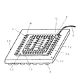
以下、この発明に係る実施の形態について、図に基づいて説明する。図1は、本発明に係るシステムインパッケージ試験検査装置(以下、SIP試験検査装置と称す)の全体構成を示す斜視図である。
図示するSIP試験検査装置100は、XYZ軸の3方向に精密移動可能な高精度移動ステージ1を備え、この高精度移動ステージ1上に高速・高周波信号を伝送可能なプリント配線基板としてのテストカード2が取り付けられている。さらに、テストカード2上には、測定するシステムインパッケージ(SIPと称す)10を装着するためのSIPソケット3が搭載されている。
Embodiments of the present invention will be described below with reference to the drawings. FIG. 1 is a perspective view showing the overall configuration of a system in package test inspection apparatus (hereinafter referred to as a SIP test inspection apparatus) according to the present invention.
The SIP test inspection apparatus 100 shown in the figure includes a high-
また、このSIP試験検査装置100は、検査用の評価信号を発生するSIP評価信号発生器6(評価信号発生手段)と、SIP10上のLSIチップにコンタクトするための微動機構付き微細高周波プローブ4(コンタクトプローブ/以下、微細高周波プローブと称す)とを備える。前記微細高周波プローブ4は、同軸ケーブル5により、SIP評価信号発生器6と接続されている。
さらに、SIP試験検査装置100は、SIP10からの出力信号を検出するSIP信号解析器7(出力信号検出手段)と、前記SIP信号解析器7が検出した信号等からデータ解析を行う制御用コンピュータ8(解析手段)とを備える。
また、テストカード2とSIP評価信号発生器6、SIP信号解析器7とは、それぞれ別の同軸ケーブル5で接続される。テストカード2とSIP用電源(LSIチップ駆動手段/図示せず)の接続は、電源ケーブル(図示せず)により接続される。
The SIP test and inspection apparatus 100 includes a SIP evaluation signal generator 6 (evaluation signal generating means) that generates an evaluation signal for inspection, and a fine high-
Further, the SIP test and inspection apparatus 100 includes a SIP signal analyzer 7 (output signal detection means) that detects an output signal from the
Further, the
前記テストカード2は、図2に示すように円形のプリント配線基板であり、基板の両側に沿って、前記同軸ケーブル5に接続されるビアホール2aが形成されており、基板の略中央における正方形の領域にはSIPソケット3用の電極端子2bが設けられている。そして、各ビアホール2aから電極端子2bに対して同軸線路2cが配列されている。
なお、テストカード2が通常のFR−4(耐燃性ガラス基材エポキシ樹脂積層板)のプリント回路基板により形成されるならば、その基板を通じて供給される信号は、100Mbps以下の比較的低速であるため、100MHz以下の低い周波数領域に限られる。したがって、本発明に係るSIP試験検査装置100においては、高周波信号に対応するため、前記したように同軸線路2cが配列されたテストカード2が用いられる。これにより、1Gbps以上の高速で、1GHz以上の高周波領域の高速・高周波の信号を扱うことが可能となり、また、各信号線間のクロストーク、外部ノイズの影響を低減させることができる。
尚、このような仕様を満たすテストカード2は、例えば株式会社神和が出願人である特許文献(特開平10−65313号公報、特開2003−349731号公報)に開示される技術を用いることにより得ることができる。
The
If the
The
また、前記微細高周波プローブ4は、高精度移動ステージ1上に設置されたプローブ支持体9の上に配置され、プローブ4の先端(コンタクト電極)は、微動機構により高精度に位置合わせできるように構成されている。測定時において微細高周波プローブ4は、真空吸着、磁力吸着などにより、コンタクト圧を得るためにプローブ支持体9に固定され、SIP10上の測定すべきLSIチップにコンタクトされる。微細高周波プローブ4の先端は、ステージ1が有する上下方向微動機構により、XYZ軸の3方向及び回転方向の位置合わせを行うことが可能になされている。
The fine high-
すなわち、図3に示すように、例えばSIP10が、入出力端子となる複数のハンダボールBが下面に形成されたLSIパッケージ71上にLSIチップ71、72、73、74、75が積層され、それぞれに形成されたボンディングパッドPがボンディングワイヤWで接続されている場合、図示するように微細高周波プローブ4の先端Gが一つのボンディングパッドPにコンタクトされる。
また、微細高周波プローブ4は、図4に示すように、微細なプローブ先端Gが多数並列に配列することにより多チャンネルに対応してもよい。尚、図4ではLSIチップ72に形成された複数のボンディングパッドPに多チャンネル微細高周波プローブ4をコンタクトする様子を示している。
That is, as shown in FIG. 3, for example, the
Further, as shown in FIG. 4, the fine high-
また、図3、図4に示す微細高周波プローブ4は、測定するLSIチップのボンディングパッド電極のピッチ(50ミクロンから150ミクロン程度)に対応して、信号電極とグランド電極の間隔が50ミクロンから100ミクロン程度の微細ピッチとなっている。
尚、この仕様を満たすプローブは、例えば、有限会社清田製作所が出願人である特許文献(特開2002―22769号公報、特開2001−311744号公報、特開2001―242193号公報、特開2000−346872号公報等)に開示された技術を用いることにより得ることができる。
Further, the fine high-
Incidentally, probes satisfying this specification are disclosed in, for example, patent documents (Japanese Patent Laid-Open No. 2002-22769, Japanese Patent Laid-Open No. 2001-31744, Japanese Patent Laid-Open No. 2001-242193, Japanese Patent Laid-Open No. -346872 etc.) and can be obtained by using the technique.
続いて、以上の構成によるSIP試験検査装置100によるSIP10に対する試験検査の手順について図5のフロー図に基づき説明する。
先ず、制御用コンピュータ8上のSIP試験検査解析プログラムに、検査するSIPの回路データおよび検査解析データを登録する(図5のステップS1)。
試験検査するSIP10をSIP用ソケット3に挿入し、SIP10上に多段積層されたLSIチップの一つに対して、微細高周波プローブ4の先端をコンタクトさせる(図5のステップS2)。
次いで、SIP用電源、SIP評価信号発生器6からテストカード2と微細高周波プローブ4を通じて、電源と評価信号をSIP10上のLSIチップに供給する(図5のステップS3)。
次いで、SIP10からテストカード2を通じて出力される信号をSIP信号解析器7により、検出する(図5のステップS4)。
そして、制御用コンピュータ8において、ステップS4において検出された信号を検査解析データと比較しながら解析する(図5のステップS5)。
Next, a test / inspection procedure for the
First, SIP circuit data and inspection analysis data to be inspected are registered in the SIP test inspection analysis program on the control computer 8 (step S1 in FIG. 5).
The
Next, the power supply and evaluation signal are supplied from the SIP power supply / SIP
Next, the signal output from the
Then, the control computer 8 analyzes the signal detected in step S4 while comparing it with the inspection analysis data (step S5 in FIG. 5).
以上のように、本発明に係る一実施の形態によれば、SIP上に多段積層されたLSIチップ間の信号線に正確にコンタクトすることのできる微細高周波プローブを用い、また、高速・高周波の信号を扱うことができるテストカードを用いることにより、高速・高周波の試験検査を高精度に行うことができる。すなわち、LSIパッケージ内に形成された配線を介さずにLSIチップに対して検査信号を入力することができ、LSIパッケージ内のインダクタンスの影響を大幅に低減でき、高周波信号を良好に伝送することができる。
したがって、SIPの製造現場において、良品検査の実施、信頼性の確保を達成することができる。また、新規回路設計のSIPに対するエラー検査にも有効に利用することができる。
As described above, according to an embodiment of the present invention, a fine high-frequency probe that can accurately contact a signal line between LSI chips stacked in multiple stages on a SIP is used, and a high-speed and high-frequency probe is used. By using a test card that can handle signals, high-speed and high-frequency test inspection can be performed with high accuracy. That is, the inspection signal can be input to the LSI chip without using the wiring formed in the LSI package, the influence of the inductance in the LSI package can be greatly reduced, and the high-frequency signal can be transmitted satisfactorily. it can.
Therefore, it is possible to achieve non-defective product inspection and ensure reliability at the SIP manufacturing site. It can also be used effectively for error inspection for SIP of a new circuit design.
尚、前記実施の形態においては、LSIパッケージとLSIチップとの接続がワイヤボンディングにより行われている場合を例に示したが、図6に示すようにLSIチップ30裏面に形成されたパッド30aとLSIパッケージ50上のパッド50aとがバンプ40によりフリップチップ接続され、接続部が露出されない場合には、図示する構造のLSIパッケージ50を採用すればよい。
すなわち、図6に示すように、LSIパッケージ50上のパッド50aから下部のハンダボール51へ至る配線の途中で、LSIチップ30の周辺領域に微細な測定パッド50bが露出するようなパッケージ構造が望ましい。このようにすれば、前記測定パッド50bに微細高周波プローブ4をコンタクトすることができ、LSIチップ30のパッド30aに近い位置から信号を入力することができる。したがって、LSIパッケージ50内に形成された配線を介さずにLSIチップ30に対して検査信号を入力することができ、LSIパッケージ30内のインダクタンスの影響を大幅に低減でき、高周波信号を良好に伝送(例えば、最大周波数40GHz、最大伝送速度10Gbps)することができる。
In the above embodiment, the case where the LSI package and the LSI chip are connected by wire bonding is shown as an example. However, as shown in FIG. 6, the pads 30a formed on the back surface of the
That is, as shown in FIG. 6, a package structure in which a fine measurement pad 50b is exposed in the peripheral region of the
本発明にかかるシステムインパッケージ試験検査装置及び試験検査方法は、半導体集積回路(LSI)チップ等の多数の電子部品を搭載した実装構造体上にシステムを構築したシステムインパッケージ(SIP)の高速・高周波電気特性を計測評価する装置及び方法に好適に用いることができる。 The system-in-package test and inspection apparatus and the test and inspection method according to the present invention provide a high-speed system-in-package (SIP) system in which a system is built on a mounting structure on which a large number of electronic components such as semiconductor integrated circuit (LSI) chips are mounted. It can be suitably used for an apparatus and method for measuring and evaluating high-frequency electrical characteristics.
1 高精度移動ステージ
2 テストカード(プリント配線基板)
3 SIPソケット
4 微動機構付き微細高周波プローブ(コンタクトプローブ)
5 同軸ケーブル
6 SIP評価信号発生器(評価信号発生手段)
7 SIP信号解析器(出力信号検出手段)
8 制御用コンピュータ(解析手段)
100 システムインパッケージ試験検査装置
1 High
3
5
7 SIP signal analyzer (output signal detection means)
8 Control computer (analysis means)
100 System in package test and inspection equipment
Claims (6)
前記システムインパッケージの入出力端子が接続されると共に、高速及び高周波信号を伝送可能なプリント配線基板と、前記LSIチップを駆動するLSIチップ駆動手段と、コンタクト電極を有し、高周波信号を伝送するコンタクトプローブと、前記コンタクトプローブに高周波の評価信号を供給する評価信号発生手段と、前記プリント配線基板を通じて前記システムインパッケージの出力信号を検出する出力信号検出手段と、前記出力信号検出手段により検出された信号を解析する解析手段とを備え、
前記コンタクトプローブのコンタクト電極を、前記LSIチップに形成された電極パッドに接触させることにより、前記LSIパッケージ内の金属配線を介さず、前記評価信号をLSIチップに入力することを特徴とするシステムインパッケージ試験検査装置。 An input / output terminal is formed on one side of an LSI package having metal wiring inside, and a plurality of LSI chips are stacked in multiple stages on the other side, and the electrical connection between the LSI chip and the LSI package and between the LSI chips A system-in-package test and inspection device that measures and evaluates high-speed and high-frequency characteristics of a system-in-package made through electrode pads formed on each of the electrical connections,
The system-in-package input / output terminal is connected, and has a printed wiring board capable of transmitting high-speed and high-frequency signals, LSI chip driving means for driving the LSI chip, and contact electrodes, and transmits high-frequency signals. A contact probe, an evaluation signal generating means for supplying a high-frequency evaluation signal to the contact probe, an output signal detecting means for detecting an output signal of the system-in-package through the printed wiring board, and detected by the output signal detecting means. And analyzing means for analyzing the received signal,
The evaluation signal is input to the LSI chip without passing through the metal wiring in the LSI package by bringing a contact electrode of the contact probe into contact with an electrode pad formed on the LSI chip. Package test inspection equipment.
高速及び高周波信号を伝送可能なプリント配線基板に、前記システムインパッケージの入出力端子を接続する工程と、
高周波信号を伝送するコンタクトプローブのコンタクト電極を、前記LSIチップに形成された電極パッドに接触させ、該電極パッドを通じてLSIチップに高周波の評価信号を入力する工程と、
前記プリント配線基板を通じて前記システムインパッケージの出力信号を検出する工程と、
前記出力信号を解析する工程とを含むことを特徴とするシステムインパッケージ試験検査方法。 An input / output terminal is formed on one side of an LSI package having metal wiring inside, and a plurality of LSI chips are stacked in multiple stages on the other side, and the electrical connection between the LSI chip and the LSI package and between the LSI chips A system-in-package test and inspection method for measuring and evaluating the high-speed and high-frequency characteristics of a system-in-package made through electrode pads formed on each of
Connecting the input / output terminals of the system-in-package to a printed wiring board capable of transmitting high-speed and high-frequency signals;
Contacting a contact electrode of a contact probe that transmits a high-frequency signal with an electrode pad formed on the LSI chip, and inputting a high-frequency evaluation signal to the LSI chip through the electrode pad;
Detecting an output signal of the system-in-package through the printed wiring board;
Analyzing the output signal, and a system in package test and inspection method.
Priority Applications (2)
| Application Number | Priority Date | Filing Date | Title |
|---|---|---|---|
| JP2004126226A JP4556023B2 (en) | 2004-04-22 | 2004-04-22 | System in package test inspection apparatus and test inspection method |
| US11/108,861 US7414422B2 (en) | 2004-04-22 | 2005-04-19 | System in-package test inspection apparatus and test inspection method |
Applications Claiming Priority (1)
| Application Number | Priority Date | Filing Date | Title |
|---|---|---|---|
| JP2004126226A JP4556023B2 (en) | 2004-04-22 | 2004-04-22 | System in package test inspection apparatus and test inspection method |
Publications (2)
| Publication Number | Publication Date |
|---|---|
| JP2005308558A true JP2005308558A (en) | 2005-11-04 |
| JP4556023B2 JP4556023B2 (en) | 2010-10-06 |
Family
ID=35135598
Family Applications (1)
| Application Number | Title | Priority Date | Filing Date |
|---|---|---|---|
| JP2004126226A Expired - Fee Related JP4556023B2 (en) | 2004-04-22 | 2004-04-22 | System in package test inspection apparatus and test inspection method |
Country Status (2)
| Country | Link |
|---|---|
| US (1) | US7414422B2 (en) |
| JP (1) | JP4556023B2 (en) |
Cited By (2)
| Publication number | Priority date | Publication date | Assignee | Title |
|---|---|---|---|---|
| JP2012532331A (en) * | 2009-07-17 | 2012-12-13 | ザイリンクス インコーポレイテッド | Apparatus and method for testing laminated die structures |
| WO2024023969A1 (en) * | 2022-07-27 | 2024-02-01 | 日本電信電話株式会社 | Pattern for inspection and integrated semiconductor circuit equipped therewith |
Families Citing this family (3)
| Publication number | Priority date | Publication date | Assignee | Title |
|---|---|---|---|---|
| JP4427645B2 (en) * | 2004-05-27 | 2010-03-10 | 独立行政法人産業技術総合研究所 | Contact probe, measurement pad used for the contact probe, and method of manufacturing the contact probe |
| US7545158B2 (en) * | 2007-04-12 | 2009-06-09 | Chroma Ate Inc. | Method for testing system-in-package devices |
| US8648615B2 (en) * | 2010-06-28 | 2014-02-11 | Xilinx, Inc. | Testing die-to-die bonding and rework |
Citations (7)
| Publication number | Priority date | Publication date | Assignee | Title |
|---|---|---|---|---|
| JPH0283475U (en) * | 1988-12-16 | 1990-06-28 | ||
| JP2000199781A (en) * | 1998-05-19 | 2000-07-18 | Advantest Corp | Semiconductor device tester and its calibration method |
| JP2001135787A (en) * | 1999-11-09 | 2001-05-18 | Rohm Co Ltd | Assembly method of semiconductor device |
| JP2001356136A (en) * | 2000-06-15 | 2001-12-26 | Advantest Corp | Integrated microcontact pin and its manufacturing method |
| JP2003307552A (en) * | 2002-04-17 | 2003-10-31 | Tokyo Electron Ltd | Contact body for signal detection and signal calibrating device |
| JP2004031649A (en) * | 2002-06-26 | 2004-01-29 | Sony Corp | Semiconductor device and its manufacturing method |
| JP2004085526A (en) * | 2001-12-05 | 2004-03-18 | Renesas Technology Corp | Semiconductor device |
Family Cites Families (16)
| Publication number | Priority date | Publication date | Assignee | Title |
|---|---|---|---|---|
| US4731577A (en) * | 1987-03-05 | 1988-03-15 | Logan John K | Coaxial probe card |
| JPH0434950A (en) * | 1990-05-30 | 1992-02-05 | Nec Corp | Semiconductor integrated circuit device |
| US5198755A (en) * | 1990-09-03 | 1993-03-30 | Tokyo Electron Limited | Probe apparatus |
| US5489852A (en) * | 1992-11-06 | 1996-02-06 | Advanced Micro Devices, Inc. | System for interfacing wafer sort prober apparatus and packaged IC handler apparatus to a common test computer |
| JPH0763788A (en) * | 1993-08-21 | 1995-03-10 | Hewlett Packard Co <Hp> | Probe, electrical part / circuit inspecting device and electrical part / method of circuit inspection |
| JPH0922929A (en) * | 1995-07-04 | 1997-01-21 | Ricoh Co Ltd | Bga package semiconductor element and inspecting method therefor |
| US6603322B1 (en) * | 1996-12-12 | 2003-08-05 | Ggb Industries, Inc. | Probe card for high speed testing |
| AU2185499A (en) * | 1998-01-30 | 1999-08-16 | Hamamatsu Photonics K.K. | Light-receiving semiconductor device with buit-in bicmos and avalanche photodiode |
| US6677776B2 (en) * | 1998-05-11 | 2004-01-13 | Micron Technology, Inc. | Method and system having switching network for testing semiconductor components on a substrate |
| US6281691B1 (en) * | 1998-06-09 | 2001-08-28 | Nec Corporation | Tip portion structure of high-frequency probe and method for fabrication probe tip portion composed by coaxial cable |
| JP2000088920A (en) * | 1998-09-08 | 2000-03-31 | Hitachi Electronics Eng Co Ltd | Interface unit for inspection apparatus |
| US6285203B1 (en) * | 1999-06-14 | 2001-09-04 | Micron Technology, Inc. | Test system having alignment member for aligning semiconductor components |
| US6433565B1 (en) * | 2001-05-01 | 2002-08-13 | Lsi Logic Corporation | Test fixture for flip chip ball grid array circuits |
| US6916682B2 (en) * | 2001-11-08 | 2005-07-12 | Freescale Semiconductor, Inc. | Semiconductor package device for use with multiple integrated circuits in a stacked configuration and method of formation and testing |
| US6822541B2 (en) * | 2002-04-25 | 2004-11-23 | Kyocera Corporation | Electromagnetic wave absorber and high-frequency circuit package using the same |
| JP4427645B2 (en) * | 2004-05-27 | 2010-03-10 | 独立行政法人産業技術総合研究所 | Contact probe, measurement pad used for the contact probe, and method of manufacturing the contact probe |
-
2004
- 2004-04-22 JP JP2004126226A patent/JP4556023B2/en not_active Expired - Fee Related
-
2005
- 2005-04-19 US US11/108,861 patent/US7414422B2/en not_active Expired - Fee Related
Patent Citations (7)
| Publication number | Priority date | Publication date | Assignee | Title |
|---|---|---|---|---|
| JPH0283475U (en) * | 1988-12-16 | 1990-06-28 | ||
| JP2000199781A (en) * | 1998-05-19 | 2000-07-18 | Advantest Corp | Semiconductor device tester and its calibration method |
| JP2001135787A (en) * | 1999-11-09 | 2001-05-18 | Rohm Co Ltd | Assembly method of semiconductor device |
| JP2001356136A (en) * | 2000-06-15 | 2001-12-26 | Advantest Corp | Integrated microcontact pin and its manufacturing method |
| JP2004085526A (en) * | 2001-12-05 | 2004-03-18 | Renesas Technology Corp | Semiconductor device |
| JP2003307552A (en) * | 2002-04-17 | 2003-10-31 | Tokyo Electron Ltd | Contact body for signal detection and signal calibrating device |
| JP2004031649A (en) * | 2002-06-26 | 2004-01-29 | Sony Corp | Semiconductor device and its manufacturing method |
Cited By (3)
| Publication number | Priority date | Publication date | Assignee | Title |
|---|---|---|---|---|
| JP2012532331A (en) * | 2009-07-17 | 2012-12-13 | ザイリンクス インコーポレイテッド | Apparatus and method for testing laminated die structures |
| KR101337071B1 (en) | 2009-07-17 | 2013-12-05 | 자일링크스 인코포레이티드 | Apparatus and method for testing of stacked die structure |
| WO2024023969A1 (en) * | 2022-07-27 | 2024-02-01 | 日本電信電話株式会社 | Pattern for inspection and integrated semiconductor circuit equipped therewith |
Also Published As
| Publication number | Publication date |
|---|---|
| US20050236717A1 (en) | 2005-10-27 |
| US7414422B2 (en) | 2008-08-19 |
| JP4556023B2 (en) | 2010-10-06 |
Similar Documents
| Publication | Publication Date | Title |
|---|---|---|
| CN102539851B (en) | High frequency probing structure | |
| US10184956B2 (en) | Probe card | |
| CN1798977B (en) | Packaging and test process, probing process and packaging test system | |
| US6232669B1 (en) | Contact structure having silicon finger contactors and total stack-up structure using same | |
| US6343940B1 (en) | Contact structure and assembly mechanism thereof | |
| US9176185B2 (en) | Active probe card for electrical wafer sort of integrated circuits | |
| EP0681186A2 (en) | Method for probing a semiconductor wafer | |
| KR20010006931A (en) | Packaging and interconnection of contact structure | |
| US8922232B2 (en) | Test-use individual substrate, probe, and semiconductor wafer testing apparatus | |
| JP5448675B2 (en) | Probe card and semiconductor wafer inspection method using the same | |
| JPWO2009041637A1 (en) | Semiconductor inspection apparatus, inspection method, and semiconductor device to be inspected | |
| CN101176008A (en) | Resilient probes for electrical testing | |
| US7825410B2 (en) | Semiconductor device | |
| JP2005010147A (en) | Module with inspection function, and its inspection method | |
| US6548756B2 (en) | Packaging and interconnection of contact structure | |
| US20140327462A1 (en) | Test socket providing mechanical stabilization for pogo pin connections | |
| US20070170935A1 (en) | Test module for wafer | |
| CN110531125B (en) | Space transformer, probe card and manufacturing method thereof | |
| US7414422B2 (en) | System in-package test inspection apparatus and test inspection method | |
| CN110010511B (en) | Test mode of radio frequency chip system-in-package module | |
| JP2009270835A (en) | Inspection method and device for semiconductor component | |
| KR20200063009A (en) | Probe card | |
| US6433565B1 (en) | Test fixture for flip chip ball grid array circuits | |
| KR101421048B1 (en) | Device For Testing Semiconductor On Mounted Active Element Chip | |
| KR20090075515A (en) | Probe card and test apparatus comprising the same |
Legal Events
| Date | Code | Title | Description |
|---|---|---|---|
| A621 | Written request for application examination |
Free format text: JAPANESE INTERMEDIATE CODE: A621 Effective date: 20070131 |
|
| A521 | Request for written amendment filed |
Free format text: JAPANESE INTERMEDIATE CODE: A523 Effective date: 20070201 |
|
| A977 | Report on retrieval |
Free format text: JAPANESE INTERMEDIATE CODE: A971007 Effective date: 20080522 |
|
| A131 | Notification of reasons for refusal |
Free format text: JAPANESE INTERMEDIATE CODE: A131 Effective date: 20080604 |
|
| A521 | Request for written amendment filed |
Free format text: JAPANESE INTERMEDIATE CODE: A523 Effective date: 20080729 |
|
| A02 | Decision of refusal |
Free format text: JAPANESE INTERMEDIATE CODE: A02 Effective date: 20090917 |
|
| A711 | Notification of change in applicant |
Free format text: JAPANESE INTERMEDIATE CODE: A711 Effective date: 20091204 |
|
| A521 | Request for written amendment filed |
Free format text: JAPANESE INTERMEDIATE CODE: A523 Effective date: 20091217 |
|
| A521 | Request for written amendment filed |
Free format text: JAPANESE INTERMEDIATE CODE: A523 Effective date: 20091204 Free format text: JAPANESE INTERMEDIATE CODE: A821 Effective date: 20091204 |
|
| A911 | Transfer to examiner for re-examination before appeal (zenchi) |
Free format text: JAPANESE INTERMEDIATE CODE: A911 Effective date: 20100107 |
|
| A01 | Written decision to grant a patent or to grant a registration (utility model) |
Free format text: JAPANESE INTERMEDIATE CODE: A01 Effective date: 20100629 |
|
| A01 | Written decision to grant a patent or to grant a registration (utility model) |
Free format text: JAPANESE INTERMEDIATE CODE: A01 |
|
| A61 | First payment of annual fees (during grant procedure) |
Free format text: JAPANESE INTERMEDIATE CODE: A61 Effective date: 20100630 |
|
| R150 | Certificate of patent or registration of utility model |
Free format text: JAPANESE INTERMEDIATE CODE: R150 |
|
| FPAY | Renewal fee payment (event date is renewal date of database) |
Free format text: PAYMENT UNTIL: 20130730 Year of fee payment: 3 |
|
| R250 | Receipt of annual fees |
Free format text: JAPANESE INTERMEDIATE CODE: R250 |
|
| S111 | Request for change of ownership or part of ownership |
Free format text: JAPANESE INTERMEDIATE CODE: R313117 |
|
| R350 | Written notification of registration of transfer |
Free format text: JAPANESE INTERMEDIATE CODE: R350 |
|
| R250 | Receipt of annual fees |
Free format text: JAPANESE INTERMEDIATE CODE: R250 |
|
| S533 | Written request for registration of change of name |
Free format text: JAPANESE INTERMEDIATE CODE: R313533 |
|
| R350 | Written notification of registration of transfer |
Free format text: JAPANESE INTERMEDIATE CODE: R350 |
|
| R250 | Receipt of annual fees |
Free format text: JAPANESE INTERMEDIATE CODE: R250 |
|
| R250 | Receipt of annual fees |
Free format text: JAPANESE INTERMEDIATE CODE: R250 |
|
| R250 | Receipt of annual fees |
Free format text: JAPANESE INTERMEDIATE CODE: R250 |
|
| LAPS | Cancellation because of no payment of annual fees |