JP2005298929A - Film deposition method - Google Patents
Film deposition method Download PDFInfo
- Publication number
- JP2005298929A JP2005298929A JP2004118953A JP2004118953A JP2005298929A JP 2005298929 A JP2005298929 A JP 2005298929A JP 2004118953 A JP2004118953 A JP 2004118953A JP 2004118953 A JP2004118953 A JP 2004118953A JP 2005298929 A JP2005298929 A JP 2005298929A
- Authority
- JP
- Japan
- Prior art keywords
- target
- film
- substrate
- refractive index
- film forming
- Prior art date
- Legal status (The legal status is an assumption and is not a legal conclusion. Google has not performed a legal analysis and makes no representation as to the accuracy of the status listed.)
- Withdrawn
Links
- 238000000151 deposition Methods 0.000 title abstract description 40
- 239000000758 substrate Substances 0.000 claims abstract description 79
- 238000000034 method Methods 0.000 claims abstract description 61
- 238000004544 sputter deposition Methods 0.000 claims abstract description 38
- 229910003087 TiOx Inorganic materials 0.000 claims abstract description 36
- HLLICFJUWSZHRJ-UHFFFAOYSA-N tioxidazole Chemical compound CCCOC1=CC=C2N=C(NC(=O)OC)SC2=C1 HLLICFJUWSZHRJ-UHFFFAOYSA-N 0.000 claims abstract description 36
- 239000000463 material Substances 0.000 claims abstract description 19
- 238000002156 mixing Methods 0.000 claims abstract description 11
- 230000015572 biosynthetic process Effects 0.000 claims description 72
- 239000007789 gas Substances 0.000 claims description 70
- 229910004298 SiO 2 Inorganic materials 0.000 claims description 36
- 150000002500 ions Chemical class 0.000 claims description 21
- 238000005192 partition Methods 0.000 claims description 18
- 229910052760 oxygen Inorganic materials 0.000 claims description 10
- 239000001301 oxygen Substances 0.000 claims description 8
- 238000007254 oxidation reaction Methods 0.000 claims description 6
- 230000003647 oxidation Effects 0.000 claims description 5
- 229910052804 chromium Inorganic materials 0.000 claims description 4
- 229910052746 lanthanum Inorganic materials 0.000 claims description 4
- 230000000670 limiting effect Effects 0.000 claims description 4
- 229910052721 tungsten Inorganic materials 0.000 claims description 4
- 229910052726 zirconium Inorganic materials 0.000 claims description 4
- 239000000203 mixture Substances 0.000 claims description 3
- 229910052758 niobium Inorganic materials 0.000 claims description 3
- -1 oxygen ions Chemical class 0.000 claims description 2
- 239000010408 film Substances 0.000 description 242
- 239000010409 thin film Substances 0.000 description 48
- 230000008021 deposition Effects 0.000 description 36
- 230000003287 optical effect Effects 0.000 description 25
- 230000008859 change Effects 0.000 description 15
- 230000007246 mechanism Effects 0.000 description 15
- 238000010521 absorption reaction Methods 0.000 description 14
- 230000000694 effects Effects 0.000 description 14
- 229910010413 TiO 2 Inorganic materials 0.000 description 10
- MYMOFIZGZYHOMD-UHFFFAOYSA-N Dioxygen Chemical compound O=O MYMOFIZGZYHOMD-UHFFFAOYSA-N 0.000 description 9
- 229910001882 dioxygen Inorganic materials 0.000 description 9
- GWEVSGVZZGPLCZ-UHFFFAOYSA-N Titan oxide Chemical compound O=[Ti]=O GWEVSGVZZGPLCZ-UHFFFAOYSA-N 0.000 description 8
- 238000002360 preparation method Methods 0.000 description 8
- 230000002829 reductive effect Effects 0.000 description 8
- 238000007796 conventional method Methods 0.000 description 7
- OGIDPMRJRNCKJF-UHFFFAOYSA-N titanium oxide Inorganic materials [Ti]=O OGIDPMRJRNCKJF-UHFFFAOYSA-N 0.000 description 7
- QVGXLLKOCUKJST-UHFFFAOYSA-N atomic oxygen Chemical compound [O] QVGXLLKOCUKJST-UHFFFAOYSA-N 0.000 description 6
- 238000002425 crystallisation Methods 0.000 description 6
- 230000008025 crystallization Effects 0.000 description 6
- 238000009826 distribution Methods 0.000 description 6
- 230000007423 decrease Effects 0.000 description 5
- XKRFYHLGVUSROY-UHFFFAOYSA-N Argon Chemical compound [Ar] XKRFYHLGVUSROY-UHFFFAOYSA-N 0.000 description 4
- 238000013461 design Methods 0.000 description 4
- 238000001552 radio frequency sputter deposition Methods 0.000 description 4
- 229910052774 Proactinium Inorganic materials 0.000 description 3
- VYPSYNLAJGMNEJ-UHFFFAOYSA-N Silicium dioxide Chemical compound O=[Si]=O VYPSYNLAJGMNEJ-UHFFFAOYSA-N 0.000 description 3
- 230000005540 biological transmission Effects 0.000 description 3
- 230000002265 prevention Effects 0.000 description 3
- 239000010936 titanium Substances 0.000 description 3
- 238000002834 transmittance Methods 0.000 description 3
- YCKRFDGAMUMZLT-UHFFFAOYSA-N Fluorine atom Chemical compound [F] YCKRFDGAMUMZLT-UHFFFAOYSA-N 0.000 description 2
- RTAQQCXQSZGOHL-UHFFFAOYSA-N Titanium Chemical compound [Ti] RTAQQCXQSZGOHL-UHFFFAOYSA-N 0.000 description 2
- 230000002159 abnormal effect Effects 0.000 description 2
- 229910052782 aluminium Inorganic materials 0.000 description 2
- 229910052786 argon Inorganic materials 0.000 description 2
- 230000008901 benefit Effects 0.000 description 2
- 239000013078 crystal Substances 0.000 description 2
- 229910052731 fluorine Inorganic materials 0.000 description 2
- 239000011737 fluorine Substances 0.000 description 2
- 238000007429 general method Methods 0.000 description 2
- 238000004519 manufacturing process Methods 0.000 description 2
- 239000012528 membrane Substances 0.000 description 2
- 229910052751 metal Inorganic materials 0.000 description 2
- 239000002184 metal Substances 0.000 description 2
- 239000005304 optical glass Substances 0.000 description 2
- 230000035699 permeability Effects 0.000 description 2
- 230000001681 protective effect Effects 0.000 description 2
- 238000005546 reactive sputtering Methods 0.000 description 2
- 238000000926 separation method Methods 0.000 description 2
- 229910052719 titanium Inorganic materials 0.000 description 2
- 101710162453 Replication factor A Proteins 0.000 description 1
- 102100035729 Replication protein A 70 kDa DNA-binding subunit Human genes 0.000 description 1
- 238000013459 approach Methods 0.000 description 1
- 230000003247 decreasing effect Effects 0.000 description 1
- 230000007547 defect Effects 0.000 description 1
- 238000010894 electron beam technology Methods 0.000 description 1
- 238000005516 engineering process Methods 0.000 description 1
- 230000001747 exhibiting effect Effects 0.000 description 1
- 230000002349 favourable effect Effects 0.000 description 1
- 239000005350 fused silica glass Substances 0.000 description 1
- 238000005304 joining Methods 0.000 description 1
- 238000010030 laminating Methods 0.000 description 1
- 229910044991 metal oxide Inorganic materials 0.000 description 1
- 150000004706 metal oxides Chemical class 0.000 description 1
- 238000012986 modification Methods 0.000 description 1
- 230000004048 modification Effects 0.000 description 1
- 230000001590 oxidative effect Effects 0.000 description 1
- 230000000149 penetrating effect Effects 0.000 description 1
- 230000000737 periodic effect Effects 0.000 description 1
- 230000003449 preventive effect Effects 0.000 description 1
- 230000008569 process Effects 0.000 description 1
- 230000003252 repetitive effect Effects 0.000 description 1
- 239000000377 silicon dioxide Substances 0.000 description 1
- 235000012239 silicon dioxide Nutrition 0.000 description 1
- 238000005477 sputtering target Methods 0.000 description 1
- 239000000126 substance Substances 0.000 description 1
- 238000001771 vacuum deposition Methods 0.000 description 1
- 238000007740 vapor deposition Methods 0.000 description 1
Images

Landscapes
- Optical Filters (AREA)
- Physical Vapour Deposition (AREA)
Abstract
Description
本発明は、光学フィルタなどの光学薄膜の成膜方法に関する。 The present invention relates to a method for forming an optical thin film such as an optical filter.
所定の波長帯域の光を遮断し、その他の波長の光を透過させる光学フィルタはマイナスフィルタと呼ばれ、一般に基板上に高屈折率層と低屈折率層とを交互に積層させた多層膜として製作されている。
このような光学フィルタにおいて、膜の屈折率を膜厚方向に周期的かつ連続的に変化させるとともに、その屈折率分布をWavelet(波束)と呼ばれる屈折率分布とした場合、透過帯域における光の透過率の周期的な変動(リップル)を原理的になくすことができる。また同時に、上述の多層膜の層数と増やすことにより、光の透過帯域と阻止帯域との境界の立ち上がりを急峻にすることができる。
An optical filter that blocks light of a predetermined wavelength band and transmits light of other wavelengths is called a minus filter, and is generally a multilayer film in which high refractive index layers and low refractive index layers are alternately laminated on a substrate. It has been produced.
In such an optical filter, when the refractive index of the film is periodically and continuously changed in the film thickness direction and the refractive index distribution is a refractive index distribution called wavelet, the transmission of light in the transmission band. The periodic fluctuation (ripple) of the rate can be eliminated in principle. At the same time, the rise of the boundary between the light transmission band and the stop band can be made steep by increasing the number of layers of the multilayer film.
しかし、Waveletの屈折率分布を有する多層膜は屈折率を連続的に変化させるため、その製造が困難であった。そこで、多層膜の製造を容易化するため、所定の屈折率を有する薄膜を積層させることにより、屈折率を細かい階段状に変化させ、Waveletの屈折率分布に近似させた各種の多層膜が提案されている。すなわち、このようなリップルのない良好な特性を示す光学フィルタを得るためには、所定屈折率の膜を形成することが必要となる。 However, a multilayer film having a Wavelet refractive index profile is difficult to manufacture because the refractive index is continuously changed. Therefore, in order to facilitate the manufacture of multilayer films, various multilayer films are proposed in which thin films having a predetermined refractive index are stacked to change the refractive index in a fine step shape and approximate the wavelet refractive index distribution. Has been. That is, in order to obtain an optical filter exhibiting such good characteristics without ripples, it is necessary to form a film having a predetermined refractive index.
上述のような所定屈折率の薄膜を形成するために、異なる屈折率の材料を混合して所定屈折率の薄膜(混合膜)を形成する方法が検討されている。この混合膜の形成にあたっては、真空蒸着法と比較して、大面積基板への成膜が可能で、薄膜形成装置内の雰囲気を安定させやすく、成膜レートが安定しているスパッタリング法が採用される傾向にある(例えば、特許文献1参照。)。
上述した特許文献1においては、二酸化シリコン(SiO2)と二酸化チタン(TiO2)との組成比を所定の比率にすることで所定屈折率の薄膜を積層させ、屈折率を細かい階段状に変化させる技術が記載されている。具体的には、融解シリカと焼結酸化チタンのターゲットを用いてRF電圧を印加することによるスパッタにより混合膜を形成している。
In
しかしながら、この方法では形成される混合膜の屈折率の上限は、TiO2のみで形成されたときの2.4程度までである。これにより、多層膜の設計自由度が下がり、多層膜を光学フィルタとして用いた場合、リップルが発生したり、阻止帯域の幅が狭くなったりする可能性があった。このような不具合を回避するために、多層膜の層数を増やすことが行われているが、層数を増やすことにより工程数が増えるため、生産性が低下するという問題があった。 However, in this method, the upper limit of the refractive index of the mixed film formed is up to about 2.4 when formed with only TiO 2 . As a result, the degree of freedom in designing the multilayer film is reduced, and when the multilayer film is used as an optical filter, ripples may occur or the width of the stop band may be narrowed. In order to avoid such a problem, the number of layers of the multilayer film is increased. However, increasing the number of layers increases the number of processes, which causes a problem that productivity decreases.
また、上述の方法では、焼結酸化チタンターゲットにRF電圧を印加することによりTiO2をスパッタしている。しかし、一般にRF電圧を印加することによるスパッタは成膜速度が遅い傾向があった。このため混合膜成膜時においてもTiO2の成膜速度が遅く、混合膜の成膜速度が遅くなって、生産性が低下するという問題があった。 In the above-described method, TiO 2 is sputtered by applying an RF voltage to the sintered titanium oxide target. However, in general, sputtering by applying an RF voltage tends to be slow in film formation. For this reason, even when the mixed film is formed, there is a problem that the film forming rate of TiO 2 is slow, the film forming rate of the mixed film is slowed, and the productivity is lowered.
あるいは、所定屈折率の薄膜を成膜する他の一般的な方法である、金属チタン(Ti)をターゲットとする反応性DCスパッタを、アルゴンガスおよび酸素ガス等を導入した雰囲気下で行い、チタン酸化物とチタン酸化物よりも屈折率の低い材料とからなる所定屈折率の混合膜を成膜することができる。この方法によれば、チタン酸化物膜の成膜速度は、上述のRF電圧を印加することによるスパッタの成膜速度よりも速いため、生産性の低下を防止することができる。 Alternatively, reactive DC sputtering using metal titanium (Ti) as a target, which is another general method for forming a thin film having a predetermined refractive index, is performed in an atmosphere into which argon gas and oxygen gas are introduced, and titanium. A mixed film having a predetermined refractive index made of an oxide and a material having a lower refractive index than titanium oxide can be formed. According to this method, since the deposition rate of the titanium oxide film is faster than the deposition rate of sputtering by applying the above-described RF voltage, it is possible to prevent a decrease in productivity.
しかしながら、この方法ではチタン酸化物膜が結晶化しやすいため、膜密度が低くなったり、膜表面が粗くなったりする恐れがあった。すると、チタン酸化物膜の結晶粒界に水分が混入しやすく、経時的にチタン酸化物膜の光学特性が変化しやすくなり耐久性が低下するなど、結晶化に起因するさまざまな問題があった。これらの結晶化に起因する問題は、混合膜においても解消されることがなかった。 However, in this method, since the titanium oxide film is easily crystallized, the film density may be lowered or the film surface may be roughened. Then, there were various problems caused by crystallization, such as moisture easily mixed into the crystal grain boundaries of the titanium oxide film, and the optical characteristics of the titanium oxide film easily changed over time, resulting in a decrease in durability. . These problems caused by crystallization were not solved even in the mixed film.
本発明は、上記の課題を解決するためになされたものであって、複数の材料から形成される混合膜を基板上に効率良く形成することができる成膜方法を提供することを目的とする。 The present invention has been made to solve the above-described problems, and an object thereof is to provide a film forming method capable of efficiently forming a mixed film formed of a plurality of materials on a substrate. .
上記目的を達成するために、以下の手段を採用する。
本発明の成膜方法は、基板上に、第1のターゲットの成分と、第2のターゲットの成分とが混合された混合膜を成膜する方法であって、TiOx(0<x<2)を主成分とする前記第1のターゲットにDC電圧を印加またはAC電圧を印加し、前記基板上に前記第1のターゲットの成分をスパッタする第1のスパッタ工程と、前記第1のターゲットと屈折率が異なる材料からなる前記第2のターゲットを前記基板上にスパッタする第2のスパッタ工程とを有することを特徴とする。
In order to achieve the above object, the following means are adopted.
The film forming method of the present invention is a method for forming a mixed film in which a component of a first target and a component of a second target are mixed on a substrate, and includes TiOx (0 <x <2). A first sputtering step in which a DC voltage or an AC voltage is applied to the first target containing as a main component, and a component of the first target is sputtered on the substrate; and the first target is refracted And a second sputtering step of sputtering the second target made of a material having a different rate onto the substrate.
すなわち、本発明の成膜方法は、第1のターゲットを用いて第1のスパッタを行い、第2のターゲットを用いて第2のスパッタを行うことにより、所定の屈折率を有する混合膜を形成する成膜方法である。混合膜の屈折率は、第1のターゲットから形成される高屈折率膜と、第2のターゲットから形成される低屈折率膜との混合割合によって2つの屈折率の間の屈折率を有する膜が形成されることになる。 That is, the film forming method of the present invention forms a mixed film having a predetermined refractive index by performing a first sputtering using a first target and performing a second sputtering using a second target. This is a film forming method. The refractive index of the mixed film is a film having a refractive index between the two refractive indexes according to the mixing ratio of the high refractive index film formed from the first target and the low refractive index film formed from the second target. Will be formed.
また、従来の方法では、TiO2は導電性がないため、ターゲットとして使用した場合、成膜速度が速いDCスパッタあるいはACスパッタは適用できず、成膜速度は遅いが導電性のないターゲットにも適用できるRFスパッタを適用せざるを得なかった。しかし、本発明の成膜方法は、第1のターゲットが、TiO2よりも酸素含有量が少なく、酸素欠損を有するTiOx(0<x<2)を主成分としているため、導電性を有し、その結果、第1のターゲットを用いて、RFスパッタよりも成膜速度の速いDCスパッタまたはACスパッタを行うことができ、混合膜の生産性を向上させることができる。
DCスパッタにおいては、例えば、異常放電防止ユニットを併用することにより、アーキングを防止して高電力を投入することができる。ACスパッタにおいては、アーキングを防止するとともに、より高速な成膜や、大面積への成膜が可能となる。
In the conventional method, since TiO 2 has no conductivity, when it is used as a target, DC sputtering or AC sputtering with a high film formation rate cannot be applied. Applicable RF sputtering had to be applied. However, the film forming method of the present invention has conductivity because the first target is mainly composed of TiOx (0 <x <2) having a lower oxygen content than TiO 2 and having oxygen vacancies. As a result, using the first target, it is possible to perform DC sputtering or AC sputtering, which has a higher deposition rate than RF sputtering, and improve the productivity of the mixed film.
In DC sputtering, for example, by using an abnormal discharge prevention unit in combination, arcing can be prevented and high power can be applied. In AC sputtering, arcing can be prevented, and film formation at a higher speed or a larger area can be achieved.
また、本発明の成膜方法により形成された混合膜はアモルファスであるため、結晶化に起因するさまざまな不具合を防止することができる。具体的には、結晶化による膜密度低下や、膜の表面が粗くなることを防止することができる。また、結晶粒界に水分が混入することが防止でき、経時的に光学特性が変化しやすくなり耐久性が劣化するといった不具合を防止することができる。 In addition, since the mixed film formed by the film forming method of the present invention is amorphous, various problems due to crystallization can be prevented. Specifically, it is possible to prevent the film density from being reduced due to crystallization and the film surface from becoming rough. In addition, it is possible to prevent moisture from entering the crystal grain boundaries, and to prevent problems such as the optical characteristics easily changing over time and the durability being deteriorated.
また、第1のターゲットから成膜された膜は、ガス導入量や酸素ガス導入割合や投入電力などの成膜条件を最適化することにより、その屈折率を、TiO2ターゲットを用いて形成された膜の屈折率2.4よりも高い2.5以上とすることができる。
さらに、混合膜の成膜中に成膜条件を変更することにより、混合膜の膜特性や混合割合を調節して、屈折率が連続的に変化する混合膜を成膜することができる。
In addition, the film formed from the first target is formed using a TiO 2 target by optimizing the film formation conditions such as the gas introduction amount, the oxygen gas introduction ratio, and the input power. The refractive index of the film can be 2.5 or higher, which is higher than 2.4.
Furthermore, by changing the film formation conditions during the formation of the mixed film, the film characteristics and the mixing ratio of the mixed film can be adjusted to form a mixed film in which the refractive index changes continuously.
また、本発明の成膜方法は、前記第1のターゲットが、Nb、Cr、Zr、Ta、Bi、Si、Ce、W、La、ALのいずれか、またはこれら成分の酸化物のいずれかを成分として含むことが望ましい。
この成膜方法によれば、第1のターゲットにNb、Cr、Zr、Ta、Bi、Si、Ce、W、La、Alのいずれか、またはこれら成分の酸化物のいずれかをその成分として含ませることにより、第1のターゲットは屈折率の高い材料となり、成膜速度も速くなる。したがって、第1のターゲットおよび第2のターゲットから形成される混合膜も、より広い範囲の屈折率を有する膜を、より速く成膜することができる。このような金属あるいは金属酸化物を第1のターゲットに含有させることにより、混合膜の光学特性や、機械的、化学的特性を改善することができるとともに、その生産性を向上させることができる。
In the film forming method of the present invention, the first target may be any one of Nb, Cr, Zr, Ta, Bi, Si, Ce, W, La, AL, or an oxide of these components. It is desirable to include it as a component.
According to this film forming method, the first target includes any one of Nb, Cr, Zr, Ta, Bi, Si, Ce, W, La, Al, or an oxide of these components as its component. By doing so, the first target becomes a material having a high refractive index, and the film forming speed is also increased. Therefore, a mixed film formed from the first target and the second target can be formed more quickly with a film having a wider range of refractive index. By including such a metal or metal oxide in the first target, the optical characteristics, mechanical and chemical characteristics of the mixed film can be improved, and the productivity can be improved.
また、本発明の成膜方法は、基板上に、多層膜を成膜する方法であって、前記多層膜のうち少なくとも一層が前記混合膜であることが望ましい。
この成膜方法によれば、任意の屈折率を有する混合膜を含む多層膜が形成できるため、従来の方法のように、所定の屈折率からなる高屈折率層と低屈折率層とを繰り返し成膜した多層膜ではリップル等の問題が発生していたが、この問題を解消したフィルター等を形成することができる。
The film forming method of the present invention is a method of forming a multilayer film on a substrate, and it is desirable that at least one of the multilayer films is the mixed film.
According to this film formation method, a multilayer film including a mixed film having an arbitrary refractive index can be formed. Therefore, as in the conventional method, a high refractive index layer and a low refractive index layer having a predetermined refractive index are repeated. The multilayer film formed has a problem such as a ripple, but a filter or the like that can solve this problem can be formed.
また、本発明の成膜方法は、前記第1のターゲットと前記第2のターゲットとが配設される領域に前記ターゲットを互いに分離して仕切る仕切り部材が配置され、前記仕切り部材により、前記第1のターゲットのスパッタと前記第2のターゲットのスパッタとが、それぞれ独立した雰囲気下で行われることが望ましい。 In the film forming method of the present invention, a partition member that separates and partitions the target from each other is disposed in a region where the first target and the second target are disposed. It is desirable that the sputtering of the first target and the sputtering of the second target are performed in independent atmospheres.
この成膜方法によれば、仕切り部材を設けることにより、仕切り部材により仕切られた雰囲気下ごとに各ターゲットの成膜条件を設定することが可能となる。すなわち、一般的な各ターゲットから飛散する材料が、他のターゲットを成膜したり、各ターゲット上に発生するプラズマが混在したりすることを防止する仕切り部材では避けることができなかったガス導入量等の条件の他方の領域に対する影響を避けることが可能となる。したがって、どちらかのターゲット付近に導入する酸素ガス量を増やせば、隣接するターゲット付近のガス量もいくらか増加するので、成膜レートに変化が生じてしまうが、仕切り部材により一方のターゲットのガス条件を変更しても、他方のターゲット付近には影響を与えないので、成膜条件の設定が容易になる。 According to this film forming method, by providing the partition member, it is possible to set the film forming conditions for each target for each atmosphere divided by the partition member. In other words, the amount of gas introduced cannot be avoided by the partition member that prevents the material scattered from each general target from forming a film on another target or mixing the plasma generated on each target. It is possible to avoid the influence of the above conditions on the other region. Therefore, if the amount of oxygen gas introduced near one of the targets is increased, the amount of gas near the adjacent target will also increase somewhat, resulting in a change in the film formation rate. Even if the change is made, there is no effect on the vicinity of the other target, so that it is easy to set the film forming conditions.
また、本発明の成膜方法は、前記第1のターゲット及び前記第2のターゲットにより混合膜を形成する際、投入する電流、投入する電圧、導入するガス量、前記基板と各ターゲットとの距離の少なくとも1つを調節することにより、前記混合膜における前記第1のターゲットの成分と前記第2のターゲットの成分との混合割合を調整することが望ましい。 Further, in the film forming method of the present invention, when the mixed film is formed by the first target and the second target, the current to be supplied, the voltage to be supplied, the amount of gas to be introduced, the distance between the substrate and each target It is desirable to adjust the mixing ratio of the first target component and the second target component in the mixed film by adjusting at least one of the above.
この成膜方法によれば、投入する電流、投入する電圧、導入するガス量、基板と各ターゲットとの距離電力といった成膜時の条件変更して、各ターゲットから基板に成膜される成膜速度を制御することにより、第1のターゲットの成分と第2のターゲットの成分との混合割合を調整する。ところで、電力を上げることにより、成膜速度を上げるという良い変化がある反面、酸化反応が追いつかず酸化の度合いが減少して、屈折率が高くなるという変化や、吸収が増加するという悪い変化が生じる。また、ガス導入量を調整して酸化ガス割合を減らすと成膜速度は速くなり、屈折率が高くなるという良い変化がある反面、吸収は増加するという悪い変化が生じる。さらに、基板とターゲットとの距離を近づければ、成膜速度は速くなるという良い変化がある反面、成膜できる面積が狭くなったり、膜厚分布が均一でなくなるなど悪い変化が生じる。ここで、投入する電流、投入する電圧、導入するガス量、基板と各ターゲットとの距離の少なくとも1つを調節することにより、これらの変化の中で所望の最適な組み合わせを選択することができるため、光学的な特性、耐久性、生産性を加味した最適な膜を形成することが可能になる。 According to this film formation method, film formation is performed from each target onto the substrate by changing the conditions at the time of film formation, such as the current to be applied, the voltage to be applied, the amount of gas to be introduced, and the distance power between the substrate and each target. By controlling the speed, the mixing ratio of the first target component and the second target component is adjusted. By the way, there is a good change to increase the deposition rate by increasing the power, but the oxidation reaction cannot catch up, the degree of oxidation decreases, the refractive index increases, and the bad change that the absorption increases. Arise. In addition, when the gas introduction amount is adjusted to reduce the ratio of the oxidizing gas, the film forming speed increases and the refractive index increases. However, there is a bad change that the absorption increases. Furthermore, if the distance between the substrate and the target is made closer, there is a good change that the film formation speed increases, but on the other hand, a bad change occurs such that the area where the film can be formed becomes narrow and the film thickness distribution becomes non-uniform. Here, by adjusting at least one of the current to be input, the voltage to be input, the amount of gas to be introduced, and the distance between the substrate and each target, a desired optimum combination can be selected among these changes. Therefore, it is possible to form an optimal film that takes into consideration optical characteristics, durability, and productivity.
また、本発明の成膜方法は、前記第1のターゲットおよび前記第2のターゲットと前記基板との間に、前記ターゲットの材料が通過可能な開口部を有する制限部材が配置され、前記制限部材には、前記開口部の開口面積を調整する調整部材が設けられ、前記調整部材により前記開口部の面積を調整することにより、前記混合膜における前記第1のターゲットの成分と前記第2のターゲットの成分との混合割合を調整することが望ましい。 Further, in the film forming method of the present invention, a limiting member having an opening through which the material of the target can pass is disposed between the first target, the second target, and the substrate, and the limiting member Is provided with an adjusting member for adjusting the opening area of the opening, and by adjusting the area of the opening by the adjusting member, the component of the first target and the second target in the mixed film It is desirable to adjust the mixing ratio with the other components.
この成膜方法によれば、成膜条件を変えることなく開口部の開口面積のみを変化させることができる。ところで、反応性スパッタにおいて、酸素ガスやアルゴンガスの流量を変化させると、成膜速度だけでなく吸収や膜密着性等が変化するので、リニアな制御が困難であり、また、電力を変化させると成膜速度にヒステリアスな変化が生じたりするため、リニアな制御が困難である。しかしながら、制限部材及び調整部材を備えることにより、プラズマ状態自体の変化を起こさないため、成膜レートをリニアに制御することが可能になる。 According to this film forming method, only the opening area of the opening can be changed without changing the film forming conditions. By the way, in reactive sputtering, if the flow rate of oxygen gas or argon gas is changed, not only the film formation speed but also absorption and film adhesion change, so that linear control is difficult and power is changed. As a result, hysteretic changes occur in the film formation speed, and linear control is difficult. However, since the limiting member and the adjusting member are provided, the plasma state itself does not change, so that the film formation rate can be controlled linearly.
また、本発明の成膜方法は、酸素イオンを導入するイオンアシスト部を配置し、前記イオンアシスト部により前記混合膜の酸化を促進することが望ましい。
この成膜方法によれば、イオンアシスト部により形成される混合膜の酸化を促進することができるので、本来酸素不足で成膜レートは速いけれども、吸収が発生するような条件においても、吸収が発生しない成膜を形成することが可能であり、成膜速度が速くなるという効果がある。
In the film forming method of the present invention, it is desirable to dispose an ion assist part for introducing oxygen ions and promote the oxidation of the mixed film by the ion assist part.
According to this film formation method, since the oxidation of the mixed film formed by the ion assist portion can be promoted, although the film formation rate is fast due to lack of oxygen originally, the absorption can be achieved even under conditions where absorption occurs. It is possible to form a film that does not occur, and there is an effect that the film forming speed is increased.
また、本発明の成膜方法は、前記第2のターゲットの成分が、Si、SiO2、SiCのいずれか、またはこれら2種類以上の混合物であることが望ましい。
この成膜方法によれば、Siを用いたDCスパッタ、SiO2を用いたRFスパッタ、SiCを用いたDCスパッタもしくはRFスパッタにより、反応ガスO2を用いて基板上にSiO2を形成するような条件でスパッタを行い、第1のターゲットと第2のターゲットとの混合膜を形成する。すなわち、SiO2は低屈折率材料の中でも吸収がなく、様々な条件で結晶化しにくいため、緻密な膜を成膜することが可能になる。
In the film forming method of the present invention, it is preferable that the component of the second target is Si, SiO 2 , SiC, or a mixture of two or more of these.
According to this film forming method, SiO 2 is formed on the substrate using the reactive gas O 2 by DC sputtering using Si, RF sputtering using SiO 2 , DC sputtering using SiC, or RF sputtering. Sputtering is performed under various conditions to form a mixed film of the first target and the second target. That is, SiO 2 is not absorbed among low refractive index materials and is difficult to crystallize under various conditions, so that a dense film can be formed.
本発明においては以下の効果を奏する。
本発明の成膜方法によれば、屈折率が2.5以上の高屈折率から低屈折材料の屈折率までの間の任意の屈折率膜を容易にかつ安定して得ることができるため、効率の良いフィルター等を形成することができる。また、第1のターゲットにDC電圧を印加することにより高速に成膜することができるため、生産性を向上させることが可能になる。さらに、形成された膜は非晶質となるため、結晶化による様々な不具合を回避することができ、良好な特性を有する膜を形成することが可能になる。
The present invention has the following effects.
According to the film forming method of the present invention, an arbitrary refractive index film between a high refractive index having a refractive index of 2.5 or more and a refractive index of a low refractive material can be obtained easily and stably. An efficient filter or the like can be formed. Further, since a film can be formed at a high speed by applying a DC voltage to the first target, productivity can be improved. Furthermore, since the formed film is amorphous, various problems due to crystallization can be avoided, and a film having favorable characteristics can be formed.
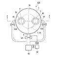
次に、本発明の第1実施形態について、図1及び図2を参照して説明する。
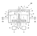
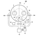
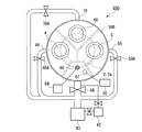
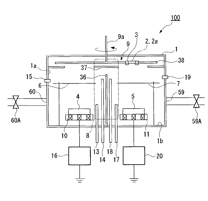
本発明の成膜方法を実施するための薄膜形成装置100について説明する。薄膜形成装置100は、図1及び図2に示すように、真空チャンバ1内に配設された光学ガラス平板からなる基板2と、この基板2に対向する同一平面上の同一円周上位置にそれぞれ配設されたスパッタリングターゲットであるSiO2ターゲット(第2のターゲット)4と、TiOx(x=1.9)ターゲット(第1のターゲット)5とを備えており、これらのターゲットをそれぞれスパッタリングして基板2上に薄膜を形成する装置である。この薄膜形成装置100は、図2に示すように、各ターゲット4,5に電力を印加する電源16,20と、ターゲット4及びターゲット5に対向する位置で回転する基板回転機構9とを備えている。
Next, a first embodiment of the present invention will be described with reference to FIGS.
A thin
各ターゲット4,5は、マグネトロンカソード10,11上に配置されている。これにより、マグネトロンカソード10は、交流電源16に接続されこの交流電源16から電力が印加されるようになっており、マグネトロンカソード11は、直流電源20に接続されこの直流電源20から電力が印加されるようになっている。
ここで、SiO2は低屈折率を有する材料として、TiOx(x=1.9)は高屈折率を有する材料として使用する。
Each of the
Here, SiO 2 is used as a material having a low refractive index, and TiOx (x = 1.9) is used as a material having a high refractive index.
基板回転機構9は、図2に示すように、基板2が配設されるヤトイ3と、真空チャンバ1の上部から内部に貫通された回転軸9aを有しヤトイ3を備える回転部材38と、回転部材38を回転させる回転モータ(図示略)とを備えている。また、基板2は、各ターゲット4,5から約105mm対向した位置に配されている。また、回転モータMは、回転部材38を10rpm以上の速度で回転させることが可能となっている。
As shown in FIG. 2, the substrate
さらに、基板回転機構9は、各ターゲット4,5の中心上方交互に基板2を通過させるように回転を行うものである。
また、基板2と各ターゲット4,5との間には、スパッタリングによってターゲット4,5から飛散された被成膜物を遮断するSiO2ターゲット4側のシャッター6及びTiOxターゲット5側のシャッター7が備えられている。また、基板2の成膜の開始と終了は、駆動系(図示略)によりシャッター6,7の開閉で行うようになっている。
Further, the
Further, between the
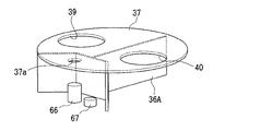
真空チャンバ1内には、各ターゲット4,5間に配設されて、これらが配設される領域を互いに分離して仕切る防着板(仕切り部材)36と、この防着板36に対して垂直に固定された上部防着板(仕切り部材)37とが備えられている。
この防着板36は排気を妨げない高さとなっており、防着板36と上部防着板37とにより、回転部材38への不要な成膜を防着するようになっている。
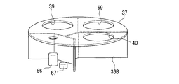
上部防着板37には、図1に示すように、Siターゲット4及びNbターゲット5に対向する位置に設けられた開放部39及び開放部40が形成されている。この開放部39,40は、各ターゲット4,5の直径より若干大きい径で形成されているため、各ターゲット4,5より飛散した被成膜物が基板2に到達するようになっている。なお、図2に示すように、防着板36は真空チャンバ1の底面に接合されていて、防着板36と上部防着板37とは直接接合されていない。ターゲット4の周囲の空間とターゲット5の周囲の空間とは、防着板36と上部防着板37との隙間を通じて繋がっている構成になっている。
In the
The
As shown in FIG. 1, an opening
また、防着板36に隣接した位置にガス導入口13,14,17,18が設けられている。これらガス導入口のうち導入口13,17は、導入されるArガスの放出部がターゲット4及びターゲット5に近接した位置に配されており、導入口14,18は、O2ガスの放出部がシャッター6,7の上方の回転部材38に近い位置に配されている。これらにより、真空チャンバ1内にArガス及びO2ガスを導入するようになっている。
Further,
また、防着板36と上部防着板37と真空チャンバ1の側壁1aと真空チャンバ1の底面1bとによって仕切られた成膜空間(スパッタリング空間)が形成されている。このそれぞれの成膜空間内と、上部防着板37の上部とを同時に排気する主排気口8がターゲット4,5に対して対称の位置となるように真空チャンバ1の側壁1aに設置されている。
また、ターゲット4側の成膜空間内を排気するように補助排気口60が、ターゲット4を挟んでガス導入口13,14に向かい合うように真空チャンバ1の側壁1aに設置されている。補助排気口60はバルブ60Aの開閉により排気の動作を行うようになっている。
一方、ターゲット5側の成膜空間内を排気するように補助排気口59が、ターゲット5を挟んでガス導入口17,18に向かい合うように真空チャンバ1の側壁1aに設置されている。補助排気口59はバルブ59Aの開閉により排気の動作を行うようになっている。
In addition, a deposition space (sputtering space) partitioned by the
Further, an
On the other hand, an
なお、ガス導入口13,14,17,18とターゲット4,5及び補助排気口59,60との位置関係は、ガス導入口13とターゲット4と補助排気口60、ガス導入口17とターゲット5と補助排気口59とがそれぞれ防着板36を挟んで対象位置で一直線上に配されていることが好ましいが、本実施例の効果としてこれに限定することはない。
The positional relationship between the
次に、以上の構成からなる薄膜形成装置100を用いて、光学薄膜を形成する本発明の成膜方法について説明する。
基板2及びヤトイ3を回転させる回転部材38の回転数は50rpm以上の高速回転が好ましく、本実施形態では、50rpmで成膜を行った。
まず、所定の屈折率(例えば1.52)を有する光学ガラス平板からなる基板2をヤトイ3にセットし、回転部材38に配置する。SiO2ターゲット4及びTiOx(x=1.9)ターゲット5等をセットし、バルブ8Aを開いた状態にし、所定の圧力(例えば7×10⁻⁵Pa)まで真空チャンバ1内を粗引きポンプ42及び高真空ポンプ43で排気する。このとき、第1,第2のバルブ59A,60Aは閉じた状態とし、補助排気口59,60からの排気は行わない。
Next, a film forming method of the present invention for forming an optical thin film using the thin
The number of rotations of the rotating
First, the
その後、主排気口8のバルブ8Aは開いた状態のまま、補助排気口59,60のバルブ59A,60Aを全開にし、補助排気を行う。全バルブを開いた後、ArガスをSiO2ターゲット4用のガス導入口13から真空計15においてトータル圧力が4×10⁻¹Paとなるまで導入し、さらに、引き続きO2ガスをガス導入口14から圧力5×10⁻¹Paとなるまで導入する。
続いて、交流電源16から300Wの交流電力を印加し、SiO2ターゲット4のSiO2上にプラズマを発生させる。これにより、3分間後に成膜準備が完了する。
Thereafter, with the
Subsequently, 300 W AC power is applied from the
同時にTiOx(x=1.9)の成膜準備も以下の手順で行う。
ArガスをTiOx(x=1.9)ターゲット5用のガス導入口17から真空計19において圧力が7×10⁻¹Paとなるまで、引き続きO2ガスをガス導入口18から圧力が1.0Paとなるまで導入する。続いて、直流電源20から300wの直流電力を印加し、TiOx(x=1.9)ターゲット5のTiOx(x=1.9)上にプラズマを発生させる。これにより、3分間後に成膜準備が完了する。
At the same time, TiOx (x = 1.9) is prepared for film formation by the following procedure.
From the
そして、成膜準備で印加した各印加電力から、SiO2ターゲット4に印加する印加電力と、TiOx(x=1.9)ターゲット5に印加する印加電力とを混合膜の屈折率に応じてそれぞれ設定した後に、SiO2ターゲット4及びTiOx(x=1.9)ターゲット5直上の各シャッター6,7を同時に開く。これにより、生成されたプラズマによってSiO2ターゲット4から弾き飛ばされたSiO2が、直上の開放部39を通過して基板2表面に到達する。同様に、TiOx(x=1.9)ターゲット5から弾き飛ばされたTiOx(x=1.9)が、直上の開放部40を通過して基板2表面に到達する。
所定の時間経過後、各シャッター6,7を同時に閉じることによって成膜が終了し、光学素子2aが得られる。
Then, from each applied power applied in the film formation preparation, an applied power applied to the SiO 2 target 4 and an applied power applied to the TiOx (x = 1.9)
After a predetermined time elapses, the
本実施形態に係る成膜方法によれば、SiO2ターゲット4を交流電圧印加によるスパッタを行った後、TiOx(x=1.9)ターゲット5をスパッタして、これらの混合膜を基板2上に形成しているため、混合膜はアモルファスとなり、結晶化に起因する種種の不具合は発生しなくなる。
According to the film forming method according to the present embodiment, after sputtering the SiO 2 target 4 by applying an alternating voltage, the TiOx (x = 1.9)
次に、本発明に係る第2実施形態について、図1及び図2を参照して説明する。なお、以下に説明する各実施形態において、上述した第1実施形態に係る薄膜形成装置100と構成を共通とする箇所には同一符号を付けて、説明を省略することにする。
本実施形態に係る薄膜形成装置100において、第1実施形態と異なる点は、第2実形態では、TiOx(x=1.9)ターゲット5に代えて、TiOx(x=0.9)ターゲット5を主成分とし、Nbの酸化物Nb2O5を約5%含有している点である。
Next, a second embodiment according to the present invention will be described with reference to FIGS. In each embodiment described below, portions having the same configuration as those of the thin
The thin
次に、以上の構成からなる薄膜形成装置100を用いて、光学薄膜を形成する本発明の成膜方法について説明する。
第1実施形態と同様に基板2及びヤトイ3を回転数50rpmで回転させ、真空チャンバ1を所定の圧力(ここでは7×10⁻⁵Pa)まで真空引きを行った後、TiOx(x=0.9)ターゲット5側にArガスを圧力が7×10⁻¹Paとなるまで導入し、O2ガスを0.9Paとなるまで導入する。直流電源20から300Wの電力を印加し、TiOx(x=0.9)ターゲット5の上にプラズマを発生させて3分間後に成膜準備が完了する。同時にSiO2ターゲット4にもArガスを圧力4×10⁻¹Paとなるまで導入し、O2ガスを4.1×10⁻¹Paとなるまで導入する。次いで、交流電源16から400W電力を印加し、Si02ターゲット4の上にプラズマを発生させて3分間後に成膜準備が完了する。シャッター6,7を同時に開き、成膜を開始する。200nmの膜厚に到達したところで、シャッター6,7を同時に閉じ、成膜を完了する。
Next, a film forming method of the present invention for forming an optical thin film using the thin
Similarly to the first embodiment, the
本実施形態に係る成膜方法によれば、TiOx(x=0.9)ターゲット5を主成分とし、Nbの酸化物Nb2O5を約5%含有しているため、酸素が少ない状態で成膜させることができるため、より高速に成膜することができる。
According to the film forming method according to the present embodiment, since the TiOx (x = 0.9)
次に、本発明に係る第3実施形態について、図3及び図4を参照して説明する。
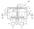
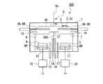
本実施形態に係る薄膜形成装置200において、第1実施形態と異なる点は、第1実形態の防着板36に代えて、上部防着板37と接合して空間を分ける仕切り部材として防着板(仕切り部材)36Aを備えている点である。
Next, a third embodiment according to the present invention will be described with reference to FIGS.
In the thin
防着板36Aは、各ターゲットの周囲を空間的に仕切る部材となっている。また、この防着板36Aは、図3及び図4に示すように、上部防着板37及び真空チャンバ1の側面に隙間なく接することで真空チャンバ1を空間的に分離している。厳密には上部方着板37の開放部39及び開放部40を通して上部でつながっているが、回転部材38は上部防着板37を覆うような位置に配されている。これにより、上部防着板37と回転部材38との隙間は0.5mm程度でできており、ターゲット4側の空間とターゲット5側の空間でガスの相互流入は少ない構成になっている。
The
本実施形態に係る成膜方法によれば、常に各ターゲット4,5には個別の条件でガスが導入されているため、一方のターゲットを有する空間のガス条件を変更しても、他方のターゲットを有する空間に影響を与えることはほとんどなく、独立にガス条件を設定することができる。また、第1実施形態においては、本実施形態に比べて空間的に分離されていないので、一方のガス条件を変更すると、他方に若干の影響を与えることになる。例えば、ターゲット4側の酸素ガス導入量を減らすと、ターゲット5側の酸素がやや少なめになり、ターゲット5側の成膜時に吸収が発生する条件になるという不都合が生じる。この場合、ターゲット5側の酸素ガス導入量を少し増やして補うといった調整が必要になる。また、場合によっては成膜レートの変化があり、条件の微調整が発生する。
According to the film forming method according to the present embodiment, gas is always introduced into each of the
なお、本実施形態では、防着板36Aにより空間的な分離が十分できる場合に効果がある。例えば、基板2やヤトイ3の形状により隙間が数cmになってしまったり、その他の原因により他の部位で空間的につながっていて、ガスの流入がある場合については、効果が得られない。
In the present embodiment, there is an effect when the spatial separation can be sufficiently performed by the
次に、本発明に係る第4実施形態について、図5及び図6を参照して説明する。
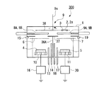
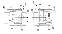
本実施形態に係る薄膜形成装置300において、第3実施形態と異なる点は、各ターゲット4,5のシャッター6,7と回転する基板2との間にスパッタリング材料の基板への到達範囲を規定する遮蔽板8,9を有する点である。
Next, a fourth embodiment according to the present invention will be described with reference to FIGS.
In the thin
遮蔽板8,9の開閉は多層を成膜する場合は層と層との間に行う。この遮蔽板8,9の開閉の原点はSiO2,TiOx(x=1.9)共に各ターゲット中心を通る垂直線上の遮蔽板8,9の面と交差する点とし、開度設定は遮蔽板8,9の開閉原点に対して両側に開く構成とした。この開き方は基板2の回転方向(図6で示す矢印A方向)に垂直な方向となっている。
The
ターゲット4側の遮蔽板8は、図6に示すように、開口制限を与える部材として機能する一対の遮蔽板(制限部材)8A,8Bの一端部を取り付けてそれぞれ直線運動可能にするボールネジ21,24と、この直線方向に一対の遮蔽板8A,8Bをガイドするガイド部材22,25と、ボールネジ21,24を所定の速度で回転駆動させるサーボモータ(調整部材)23,26とを備えている。同様にターゲット5側の遮蔽板9は、一対の遮蔽板(制限部材)9A,9Bの一端部を取り付けてそれぞれ直線運動可能にするボールネジ27,30と、ガイド部材29,31と、サーボモータ(調整部材)28,32とを備えている。また、遮蔽板8,9は、一対の遮蔽板8A,8Bまたは9A,9Bの閉口位置を確認する位置センサ33を備えている。これらの位置センサ33は、原点位置として電気的に検出するものである。また、各サーボモータは、遮蔽板8A,8B及び遮蔽板9A,9Bにより形成され各ターゲット4,5の材料が通過可能な開口部8a及び9aの開口幅(開口面積)を調整可能となっている。
As shown in FIG. 6, the shielding
次に、以上の構成からなる薄膜形成装置300を用いて、光学薄膜を形成する本発明の成膜方法について説明する。
まず、各ターゲットの遮蔽板8A,8B及び遮蔽板9A,9Bを調整し、開口部8a,9aを表1に示す条件に設定する。そして、基板2及びヤトイ3を回転数200rpmで回転させ、真空チャンバ1を所定の圧力(ここでは3×10⁻⁵Pa)まで真空引きを行った後、ターゲット4側にはArガスを7×10⁻¹Paまで導入し、続いて、O2ガスを9×10⁻¹Paまで導入してRF電圧250Wを印加する。また、ターゲット5側には、Arガスを6×10⁻¹Pa導入し、続いて、O2ガスを7×10⁻¹Paまで導入してDC電圧400Wを印加する。2分間ほどプレスパッタした後、基板2上に成膜を開始した。NO.1〜NO.5までそれぞれの条件下でSiO2開口部とTiOx開口部とを変化させて成膜を実施することにより、基板2には表1に示す屈折率及び成膜速度からなる膜が得られた。
Next, the film forming method of the present invention for forming an optical thin film using the thin
First, the
本実施形態に係る成膜方法によれば、開口部8a,9aを変更して成膜条件を変更することにより、プラズマ状態への影響が少なくレートをリニアに変更できるという利点がある。例えば、電力を変更すると、レート以外にヒステリシスや吸収といった変化がある。また、ガスを変更すると、レート以外に吸収の発生が生じる。また、距離の変更では、レート以外に分布の変化がある。このようなことを補正するには制御する項目が多くなるという欠点があったが、開口部8a,9aをパラメータとすることでこういった欠点を解消することができる。
The film forming method according to the present embodiment has an advantage that the rate can be changed linearly with little influence on the plasma state by changing the film forming conditions by changing the
なお、本実施形態では、遮蔽板8,9の開閉は多層を行う場合は層と層との間に行ったが、成膜中に遮蔽板8,9の開閉を行うことも可能である。この場合、遮蔽板8,9の開閉により混合割合が変化するので、屈折率が膜厚に対して連続的に変化する任意屈折率を形成することも可能である。
In the present embodiment, the
次に、本発明に係る第5実施形態について、図7及び図8を参照して説明する。
本実施形態に係る薄膜形成装置400において、第4実施形態と異なる点は、基板2の回転軌道上の直下にイオン照射機構(イオンアシスト部)66を配置している点である。
イオン照射機構66は、図7及び図8に示すように、ターゲット4(SiO2)とターゲット5(TiOx)(x=1.9)を仕切る略Y字型の防着板36Aと、上方の上部防着板37とで形成された空間に配置されると共に、上部防着板37に形成された開口37aから、回転中の基板2に対してイオン照射できるようになっている。これは、開口37aが、図8に示すように、イオン照射機構66のイオン照射部の大きさと略一致しているからである。
Next, a fifth embodiment according to the present invention will be described with reference to FIGS.
The thin
As shown in FIGS. 7 and 8, the
イオン照射機構66が配置される空間は、各ターゲット4,5が配置される空間よりも高真空となるように、高真空ポンプ43と連結された排気口に接続されている。そして、この空間内でイオン照射機構66は、電源64から供給される電力によって駆動される。また、異常放電を防止する目的からマイナスイオンを供給するニュートラライザー67をイオン照射機構66の脇に設置し、操作用電源65で操作するようになっている。
The space in which the
次に、以上の構成からなる薄膜形成装置400を用いて、光学薄膜を形成する本発明の成膜方法について説明する。
まず、各ターゲットの遮蔽板8A,8B及び遮蔽板9A,9Bを調整し、開口部を表2に示す条件に設定する。そして、基板2及びヤトイ3を回転数120rpmで回転させ、真空チャンバ1を所定の圧力(ここでは2×10⁻⁵Pa)まで真空引きを行った後、ターゲット4側にはArガスを6×10⁻¹Paまで導入し、続いて、O2ガスを7×10⁻¹Paまで導入してRF電圧250Wを印加し、3分間ほどプレスパッタした。ターゲット5側には、Arガスを8×10⁻¹Paまで導入して、続いてO2ガスを9×10⁻¹Pa導入して、DC電圧400Wを印加し、3分ほどプレスパッタした。この工程と同時にニュートラライザー67にガス導入口(図示略)からArガスを7×10⁻¹Paまで導入し、150Aの電流を印加し、電子線を引き出しイオン照射機構66周辺に電子を供給する。イオン照射機構66の内部にO2ガス15sccm流し、イオン照射機構66に500Wの電力を印加してO2をイオン化して照射の準備をした。そして、成膜を開始した。
NO.1〜NO.5までそれぞれの条件下でSiO2開口部とTiOx開口部を変化させて成膜を実施することにより、基板2には表2に示す屈折率及び成膜速度からなる膜が得られた。
Next, a film forming method of the present invention for forming an optical thin film using the thin
First, the
NO. 1-NO. By carrying out film formation by changing the SiO 2 opening and the TiOx opening under the respective conditions up to 5, a film having a refractive index and a film formation speed shown in Table 2 was obtained on the
第4実施形態と比較すると、屈折率はやや高めの1.47から2.47の任意の屈折率が得られた。また、第4実施形態と同様の屈折率2.18の膜と比較すると、本実施形態の方が成膜速度が速くなっている。 As compared with the fourth embodiment, an arbitrary refractive index of 1.47 to 2.47, which is a slightly higher refractive index, was obtained. In addition, compared with a film having a refractive index of 2.18 similar to that of the fourth embodiment, the film formation speed of this embodiment is higher.
本実施形態に係る成膜方法によれば、イオン照射機構66により形成される混合膜の酸化を促進することができるので、本来酸素不足では成膜レートが速いが、吸収が発生するような条件においても、吸収が発生しない薄膜を形成することが可能であり、成膜速度が速くなるという効果がある。一般に反応性スパッタにおいては、酸素ガスの導入量を少なくすると成膜速度が速くなるという利点はあるが、混合膜においては吸収が発生するという欠点があり光学特性が劣化する。そのため、吸収が光学特性上問題のないレベルまで酸素ガスを少なくした条件の中で成膜速度をあげるといった取り組みを行っている。
According to the film forming method according to the present embodiment, the oxidation of the mixed film formed by the
また、表2中のNO.1,NO.3,NO.5の同じ条件で屈折率2.54,1,95,1.47の薄膜を各5バッチずつ成膜して屈折率のばらつきを確認したところ、条件1は2.54±0.03,条件3は1.95±0.03,条件5は1.47±0.02となった。したがって、第1実施形態で行った実施例1と比較して、屈折率±0.03の範囲内とおよそ半分のばらつき範囲で、任意の屈折率膜についての再現性が得られた。
In addition, NO. 1, NO. 3, NO. 5 thin films having refractive indexes of 2.54, 1, 95, and 1.47 were formed in batches of 5 under the same conditions of 5 and the variation in refractive index was confirmed.
次に、本発明に係る第6実施形態について、図9を参照して説明する。
本実施形態に係る薄膜形成装置500において、第4実施形態と異なる点は、ターゲット4としてSiO2を用いたが、これに代えて、MgF2を用いることと、ターゲット4とマグネトロンカソード10との間にはSiO2からなる断熱板80を換装していることである。
Next, a sixth embodiment according to the present invention will be described with reference to FIG.
In the thin
次に、以上の構成からなる薄膜形成装置500を用いて、光学薄膜を形成する本発明の成膜方法について説明する。
まず、基板2及びヤトイ3を回転数120rpmで回転させ、真空チャンバ1を所定の圧力(例えば5×10⁻⁵Pa)まで真空引きを行った後、ターゲット4側にはArガスを7×10⁻¹Paまで導入し、続いて、O2ガスを9×10⁻¹Paまで導入してRF電圧200Wを印加した。そして、ターゲット5側にはArガスを5×10⁻¹Paまで導入し、続いて、O2ガスを6×10⁻¹Paまで導入してDC電圧350Wを印加し、3分間ほどプレスパッタした。
Next, a film forming method of the present invention for forming an optical thin film using the thin
First, the
その後、NO.1〜NO.5までそれぞれの条件下でSiO2開口部とTiOx開口部を変化させて成膜を実施することにより、基板2には表3に示す屈折率及び成膜速度からなる膜が得られた。
After that, NO. 1-NO. By performing film formation while changing the SiO 2 opening and the TiOx opening under the respective conditions up to 5, a film having a refractive index and a film formation speed shown in Table 3 was obtained on the
本実施形態に係る成膜方法によれば、低屈折率ターゲットとしてMgF2を用いているため、低屈折率の幅が1.38という低い屈折率から2.53という高い屈折率までを形成できるようになる。これにより、特性の良いフィルター等を形成することが可能になる。また、通常MgF2をターゲットとしてスパッタで膜を形成するとフッ素が乖離して吸収膜が形成されてしまい、光学特性としての利用が難しい。しかしながら、本実施形態では、断熱板80を介しているため、ターゲット4が高い表面温度を維持することにより蒸着に近い現象を起こし、フッ素の乖離を抑えることができる。これにより、基板2上に吸収の少ないMgF2からなる低屈折膜を形成することができ、ターゲット5との混合膜を基板上に成膜することが可能になる。
According to the film forming method of this embodiment, since MgF 2 is used as the low refractive index target, the low refractive index width can be formed from a low refractive index of 1.38 to a high refractive index of 2.53. It becomes like this. This makes it possible to form a filter with good characteristics. In addition, when a film is formed by sputtering with MgF 2 as a target, fluorine is separated and an absorption film is formed, which makes it difficult to use as an optical characteristic. However, in the present embodiment, since the
次に、本発明に係る第7実施形態について、図10及び図11を参照して説明する。
本実施形態に係る薄膜形成装置600において、第5実施形態と異なる点は、ターゲット4としてSiからなるターゲットを備えている点、ターゲット5に加えてTiOx(x=1.9)ターゲット68を備えている点,防着板(仕切り部材)36Bの形状及び補助排気口70を備えている点である。
Next, a seventh embodiment according to the present invention will be described with reference to FIGS.
The thin
ターゲット4には、図10に示すように、電力を供給する直流電源16が備えられている。
防着板36Bは、ターゲット4,5,68を仕切る略Y字形の形状になっている。また、上部防着板37には、ターゲット68の上方に位置する箇所に、ターゲット68の直径より若干大きい径で形成され開放部69が設けられている。これにより、ターゲット68より飛散した被成膜物が基板2に到達するようになっている。
また、開放部69の上部には遮蔽板(図示略)が配されている。この遮蔽板は図6に示す遮蔽板8,9と同様の開口機構を有していて、ターゲット68の材料が通過可能な開口幅を調整可能となっている。
補助排気口70は、バルブ70Aの開閉により排気の動作を行うようになっている。
As shown in FIG. 10, the
The
In addition, a shielding plate (not shown) is disposed on the upper portion of the opening
The
次に、以上の構成からなる薄膜形成装置600を用いて、光学薄膜を形成する本発明の成膜方法について説明する。
まず、第5実施形態と同様にして基板2及びヤトイ3を回転させ、真空チャンバ1の真空引きを行った後、ターゲット4側にはArガスを7×10⁻¹Paまで導入し、続いて、O2ガスを1.1Paまで導入してDC電圧350Wを印加し、3分間ほどプレスパッタした。そして、ターゲット5及びターゲット68側にはArガスを4×10⁻¹Paまで導入し、続いて、O2ガスを5×10⁻¹Paまで導入してDC電圧400Wを印加し、3分間ほどプレスパッタした。その後、同時にシャッター6,7,7を開けて成膜を開始する。
Next, a film forming method of the present invention for forming an optical thin film using the thin
First, the
本実施形態に係る成膜方法によれば、第1実施形態の薄膜形成装置100により行った実施例1での屈折率が2.49になる膜を形成した場合の成膜速度は1.1nm/minであるのに対し、成膜速度は2nm/minであり、速い速度で成膜が可能である。また、ターゲット5,68にはAC電圧を印加することも可能であり、この場合も同様の効果を得ることができる。なお、ACスパッタにおいてはアーキング防止すると共に、より高速な成膜や大面積の成膜が可能となる。また、比較的高屈折率な混合膜を得る場合、TiOx(x=1.9)のターゲットを2個備えているため、成膜速度を速くすることができ、生産性が向上する。
なお、比較的高屈折率な膜の形成に限らず、比較的低屈折率な膜を形成する場合には、ターゲット68に代えて、Si,SiO2,SiC等からなるターゲットを2個搭載する構成にすることにより、比較的低屈率な膜を速い成膜速度で得ることができる。
According to the film forming method according to the present embodiment, the film forming speed when the film having the refractive index of 2.49 in Example 1 performed by the thin
When forming a film having a relatively low refractive index, not limited to forming a film having a relatively high refractive index, two targets made of Si, SiO 2 , SiC, or the like are mounted instead of the
なお、本発明の技術範囲は上記実施の形態に限定されるものではなく、本発明の趣旨を逸脱しない範囲において種々の変更を加えることが可能である。
例えば、第1実施形態において、バルブ59A,60Aを全開/全閉のバルブに変えてコンダクタンス・バルブとし、ガス圧に合わせて可変としても本実施形態の効果を妨げることはない。
The technical scope of the present invention is not limited to the above embodiment, and various modifications can be made without departing from the spirit of the present invention.
For example, in the first embodiment, the effect of the present embodiment is not hindered by changing the
また、回転部材38と上部防着板37との距離は近いほど防着板としての効果が高く、0.5mm〜30mmが好ましい。0.5mm未満の距離だと成膜開始のできる排気到達まで時間がかかるが、回転部材38と上部防着板37とが正確に水平出しがしてあれば問題はない。一方、回転部材38と上部防着板37との距離が30mmより長い距離である場合、他の成膜空間への導入ガス流入の可能性があるが、上部防着板37に設けられた開放部39,40の大きさを基板2の径より小さくならない程度に小さくする方向で調整することにより、回転部材38と上部防着板37との距離を50mmまでとることができる。また、スパッタリング放電(放電を発生させる投入パワーに依存する)を遮ることがなければ、さらに距離を長くすることが可能となる。
Further, the closer the distance between the rotating
上記第1実施形態に基づいて基板2上に混合膜からなる光学薄膜を形成した結果を以下に示す。
成膜準備の印加電力から各々表4の5種類(NO.1〜NO.5)の条件の印加電力の1つに調整し、シャッター6,7を同時に開き、成膜を開始する。そして、200nmの膜厚に到達したところでシャッター6,7を同時に閉じ、成膜を完了する。このようにして、5種類の条件をそれぞれの印加電力で、基板2をそれぞれ交換しながら、混合膜を成膜した。このときの、5種類の条件で電力を印加したときに得られた基板2上に成膜された膜の屈折率と成膜速度の関係を表4に示す。
The result of forming an optical thin film made of a mixed film on the
The applied power for film formation preparation is adjusted to one of the five types (NO. 1 to NO. 5) of applied power in Table 4, and the
表4中のNO.2〜NO.4の同じ条件で屈折率2.41,1,90,1.61を各5バッチずつ成膜して屈折率のばらつきを確認したところ、条件2は2.41±0.04,条件3は1.90±0.03,条件4は1.61±0.03となった。したがって、1.46〜2.53の範囲内の屈折率が任意に得られ、また、同じ条件で繰り返し再現性については、ばらつきが各屈折率±0.05の範囲内と安定した屈折率を得ることができる。さらに、成膜された膜を分析したところ結晶性は見られず、アモルファスであった。
NO. In Table 4 2 to NO. When the refractive index variation was confirmed by depositing 5 batches of refractive indexes 2.41, 1, 90, and 1.61 under the same conditions of 4, the
本実施例1による成膜速度は、屈折率が2.41の膜を形成する場合、1.1nm/minであった。本発明の効果を確認するため、比較として、図1と同様の構成で同じ屈折率を得るために、TiOx(x=1.9)ターゲット5の代わりにTiO2及び高周波電源20を用いてRF電圧を印加する従来の成膜方法を示す。
The deposition rate according to the first example was 1.1 nm / min when a film having a refractive index of 2.41 was formed. In order to confirm the effect of the present invention, as compared, in order to obtain the same refractive index the same configuration as FIG. 1, with the TiO 2 and the high-
第1実施形態と同様にして、SiO2ターゲット4のSiO2上にプラズマを発生させて、3分間後に成膜準備が完了する。続いて、第1実施形態と同様にして、ガス導入口18から圧力が1.0Paとなるまで導入する。次いで、高周波電源20から400Wの電力を印加し、ターゲット5のTiO2上にプラズマを発生させ、3分間後に成膜準備が完了する。
この結果、成膜された膜の屈折率は2.41であり、このときの、成膜速度は0.3nm/minであった。この従来の方法と比較すると、本実施例1では成膜速度が速く、生産性に優れていると言える。
In the same manner as in the first embodiment, plasma is generated on the SiO 2 of the SiO 2 target 4 and film formation preparation is completed after 3 minutes. Then, it introduce | transduces until the pressure becomes 1.0 Pa from the
As a result, the refractive index of the formed film was 2.41, and the film formation speed at this time was 0.3 nm / min. Compared with this conventional method, it can be said that the film forming speed is higher in Example 1 and the productivity is excellent.
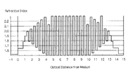
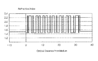
上記第1実施形態に基づいて基板2上に、図12に示す横軸に膜厚、縦軸に屈折率に示す設計値にしたがって、任意屈折率により順次積層してノッチフィルターを形成する。
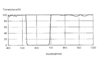
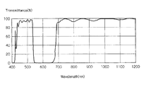
本実施例2では第1実施形態に示される成膜方法により形成された混合膜を含む多層膜を形成する。具体的には、SiO2ターゲット4にRF電圧280Wを印加して、TiOx(x=1.9)ターゲット5にDC電圧200Wを印加して形成した屈折率1.5からSiO2ターゲット4にRF電圧180Wを印加して、TiOx(x=1.9)ターゲット5にDC電圧300Wを印加して形成した屈折率2.3の間の屈折率を有する膜を形成する。これは、屈折率1.52の基板上に多層膜を形成して、もう一枚の屈折率1.52の基板に接合した状態を示している。基本的には、低屈折率層と高屈折率層とを繰り返す構成となっている。すなわち、屈折率1.5から屈折率2.3を繰り返す層があり、その前後を、基板から徐々に屈折率1.5に近づけて行く低屈折率層と、基板から徐々に屈折率2.3に近づけていく高屈折率層を繰り返す層からなる構成となっている。なお、繰り返し層の両付近の層はリップルが少なくなるように屈折率が最適化された設計となっている。このようにして得られた多層膜の特性を横軸に波長、縦軸に透過率として図13に示す。
Based on the first embodiment, a notch filter is formed on the
In Example 2, a multilayer film including a mixed film formed by the film forming method shown in the first embodiment is formed. Specifically, RF and applying an RF voltage 280W to SiO 2 target 4, the refractive index of 1.5 was formed by applying a DC voltage 200W to TiOx (x = 1.9)
本実施例2によれば、阻止帯域の両側には、ほとんどリップルは発生していない。本発明の効果を確認するため、比較として、従来の方法により、図14に示すように、高屈折率側が2.3のTiO2と、低屈折率側の屈折率が1.46のSiO2を積層する構成の設計値にしたがって成膜を行う。図14においても、屈折率1.52の基板上に多層膜を形成して、もう一枚の屈折率1.52の基板に接合した状態を示している。この従来の方法では、ノッチフィルターの阻止帯域の両側にリップルを極力低減するための各層の膜厚を最適化している。こうして得られた多層膜特性は、図15に示すように、従来の一般的な成膜方法で得られるフィルターでは、阻止帯域の両側のリップルが発生してしまう。したがって、本実施例では従来の一般的な方法と比較して、リップルが少ない良好な特性をえることができる。 According to the second embodiment, almost no ripple is generated on both sides of the stop band. In order to confirm the effect of the present invention, as compared, in a conventional manner, as shown in FIG. 14, and TiO 2 of high refractive index side is 2.3, SiO 2 of the low refractive index side of the refractive index is 1.46 The film is formed in accordance with the design value of the configuration in which the layers are stacked. FIG. 14 also shows a state in which a multilayer film is formed on a substrate having a refractive index of 1.52 and bonded to another substrate having a refractive index of 1.52. In this conventional method, the film thickness of each layer is optimized to reduce ripple as much as possible on both sides of the stop band of the notch filter. As shown in FIG. 15, the multilayer film characteristics obtained in this way cause ripples on both sides of the stop band in a filter obtained by a conventional general film forming method. Therefore, in this embodiment, it is possible to obtain good characteristics with less ripple as compared with the conventional general method.
上記第2実施形態に基づいて基板2上に混合膜からなる光学薄膜を形成した結果を以下に示す。
基板2上に成膜された膜の屈折率は2.41であった。このときの成膜速度は1.6nm/minであった。本発明の効果を確認するため、比較として、図1と同様の構成で同じ屈折率を得るために、TiO2ターゲット5にRF電圧を印加し成膜を行うと、0.3nm/minであった。したがって、従来の方法と比較すると成膜速度が速く、生産性に優れていることが言える。なお、Nbの酸化物以外に、Cr、Zr、Ta、Bi、Si、Ce、W、La及びAlからなる酸化物を含有した場合において同様の効果を得ることができる。また、第1実施形態と同様の構成で屈折率2.41の膜を形成する場合、成膜速度は1.1nm/minであった。本実施例2では、ターゲットは酸化しやすく、酸素が少なくても良いため成膜速度が速く、より高速な成膜が可能である。
The result of forming an optical thin film made of a mixed film on the
The refractive index of the film formed on the
上記第3実施形態に基づいて基板2上に混合膜からなる光学薄膜を形成した結果を以下に示す。
本実施例では、SiO2ターゲット4あるいはTiOx(x=0.2)ターゲット5に導入するガスを変化させることにより屈折率を制御した。
まず、基板2及びヤトイ3を回転数80rpmで回転させ、真空チャンバ1に所定の圧力(4×10⁻⁵Pa)まで真空引きを行った後、ターゲット4側には表5のNO.1に示す条件でガスを導入してRF電圧400Wを印加する。ターゲット5にも同様に表5のNO.1に示す条件でガスを導入してDC電圧400Wを印加する。これにより、表5のNO.1に示す屈折率の混合膜が得られた。また、同様にして、表5のNO.2,NO.3に示す条件で、同様の電力を印加して、それぞれの屈折率の膜が得られた。
The result of forming an optical thin film made of a mixed film on the
In this example, the refractive index was controlled by changing the gas introduced into the SiO 2 target 4 or the TiOx (x = 0.2)
First, the
ガス条件と成膜速度あるいはガス条件と吸収との間には、酸素ガスの割合を減らすと成膜速度は速くなり、屈折率が高くなるという変化がある反面、吸収は増加すると言う悪い変化がある。また、電力,電流,電圧のいずれかを上げれば成膜速度は上がり、電力,電流,電圧のいずれかを下げれば成膜速度は下がるという変化がある。これらの現象は混合膜にも反映されるので、所望の光学特性に応じてパラメータを選択すればよい。また、ターゲットと基板との距離を近づければ、成膜速度は速くなるという変化がある反面、成膜できる面積が狭くなり、分布も生じてくるという悪い変化もある。こういう変化を所望の光学特性に応じて利用しても良い。 There is a change between the gas condition and the film formation rate or between the gas condition and the absorption that the film formation speed increases and the refractive index increases when the proportion of oxygen gas is reduced, while the absorption increases. is there. Further, there is a change that the film formation rate increases when any one of power, current, and voltage is increased, and the film formation rate decreases when any one of power, current, and voltage is decreased. Since these phenomena are also reflected in the mixed film, parameters may be selected according to desired optical characteristics. In addition, if the distance between the target and the substrate is reduced, the film forming speed is increased. On the other hand, there is also a bad change that the area where the film can be formed is reduced and the distribution is generated. Such changes may be used according to desired optical characteristics.
2 基板
4 SiO2ターゲット(第2のターゲット)
5 TiOxターゲット(第1のターゲット)
8A,8B,9A,9B 一対の遮蔽板(制限部材)
8a,9a 開口部
23,26,28,32 サーボモータ(調整部材)
36 防着板(仕切り部材)
37 上部防着板(仕切り部材)
66 イオン照射機構(イオンアシスト部)
2
5 TiOx target (first target)
8A, 8B, 9A, 9B A pair of shielding plates (restriction members)
8a,
36 Protection plate (partition member)
37 Upper protective plate (partition member)
66 Ion irradiation mechanism (ion assist part)
Claims (8)
TiOx(0<x<2)を主成分とする前記第1のターゲットにDC電圧を印加またはAC電圧を印加し、前記基板上に前記第1のターゲットの成分をスパッタする第1のスパッタ工程と、
前記第1のターゲットと屈折率が異なる材料からなる前記第2のターゲットを前記基板上にスパッタする第2のスパッタ工程とを有することを特徴とする成膜方法。 A method of forming a mixed film in which a component of a first target and a component of a second target are mixed on a substrate,
Applying a DC voltage or an AC voltage to the first target containing TiOx (0 <x <2) as a main component, and sputtering the components of the first target on the substrate; ,
A film forming method comprising: a second sputtering step of sputtering the second target made of a material having a refractive index different from that of the first target onto the substrate.
前記多層膜のうち少なくとも一層が前記混合膜であることを特徴とする請求項1または請求項2に記載の成膜方法。 A method of forming a multilayer film on a substrate,
The film forming method according to claim 1, wherein at least one of the multilayer films is the mixed film.
前記仕切り部材により、前記第1のターゲットのスパッタと前記第2のターゲットのスパッタとが、それぞれ独立した雰囲気下で行われることを特徴とする請求項1から請求項3のいずれか1項記載の成膜方法。 A partition member that separates and partitions the targets from each other is disposed in a region where the first target and the second target are disposed;
4. The sputter of the first target and the sputter of the second target are performed by the partition member in independent atmospheres, respectively. 5. Film forming method.
前記制限部材には、前記開口部の開口面積を調整する調整部材が設けられ、
前記調整部材により前記開口部の面積を調整することにより、前記混合膜における前記第1のターゲットの成分と前記第2のターゲットの成分との混合割合を調整することを特徴とする請求項1から請求項5のいずれか1項に記載の成膜方法。 A limiting member having an opening through which the material of the target can pass is disposed between the first target and the second target and the substrate,
The restriction member is provided with an adjustment member for adjusting the opening area of the opening,
The mixing ratio of the component of the first target and the component of the second target in the mixed film is adjusted by adjusting the area of the opening by the adjusting member. The film forming method according to claim 5.
前記イオンアシスト部により前記混合膜の酸化を促進することを特徴とする請求項1から請求項6のいずれか1項に記載の成膜方法。 An ion assist part that introduces oxygen ions is placed,
The film forming method according to claim 1, wherein oxidation of the mixed film is promoted by the ion assist unit.
The film formation according to any one of claims 1 to 7, wherein a component of the second target is any one of Si, SiO 2 , and SiC, or a mixture of two or more of these. Method.
Priority Applications (1)
| Application Number | Priority Date | Filing Date | Title |
|---|---|---|---|
| JP2004118953A JP2005298929A (en) | 2004-04-14 | 2004-04-14 | Film deposition method |
Applications Claiming Priority (1)
| Application Number | Priority Date | Filing Date | Title |
|---|---|---|---|
| JP2004118953A JP2005298929A (en) | 2004-04-14 | 2004-04-14 | Film deposition method |
Publications (1)
| Publication Number | Publication Date |
|---|---|
| JP2005298929A true JP2005298929A (en) | 2005-10-27 |
Family
ID=35330838
Family Applications (1)
| Application Number | Title | Priority Date | Filing Date |
|---|---|---|---|
| JP2004118953A Withdrawn JP2005298929A (en) | 2004-04-14 | 2004-04-14 | Film deposition method |
Country Status (1)
| Country | Link |
|---|---|
| JP (1) | JP2005298929A (en) |
Cited By (2)
| Publication number | Priority date | Publication date | Assignee | Title |
|---|---|---|---|---|
| JP2009066497A (en) * | 2007-09-12 | 2009-04-02 | Bridgestone Corp | Photocatalyst thin film of titanium oxide and its production method |
| JP2009139925A (en) * | 2007-11-16 | 2009-06-25 | Epson Toyocom Corp | Optical multilayer filter, optical multilayer filter manufacturing method, and electronic apparatus |
-
2004
- 2004-04-14 JP JP2004118953A patent/JP2005298929A/en not_active Withdrawn
Cited By (2)
| Publication number | Priority date | Publication date | Assignee | Title |
|---|---|---|---|---|
| JP2009066497A (en) * | 2007-09-12 | 2009-04-02 | Bridgestone Corp | Photocatalyst thin film of titanium oxide and its production method |
| JP2009139925A (en) * | 2007-11-16 | 2009-06-25 | Epson Toyocom Corp | Optical multilayer filter, optical multilayer filter manufacturing method, and electronic apparatus |
Similar Documents
| Publication | Publication Date | Title |
|---|---|---|
| JP5162618B2 (en) | Method for producing a multilayer film and apparatus for carrying out said method | |
| WO2010018639A1 (en) | Deposition apparatus and method for manufacturing thin-film device | |
| US12523797B2 (en) | Optical device and manufacturing method therefor | |
| US20160254127A1 (en) | Method and device for producing uniform films on moving substrates and films produced in this way | |
| US20120164051A1 (en) | Method for the production of oxide and nitride coatings and its use | |
| KR20190038430A (en) | Film forming apparatus | |
| JP5252831B2 (en) | Dielectric multilayer filter manufacturing method and dielectric multilayer filter manufacturing apparatus | |
| JP5697829B2 (en) | Method for producing a multilayer film and apparatus for carrying out said method | |
| US20040182701A1 (en) | Sputtering apparatus, a mixed film produced by the sputtering apparatus and a multilayer film including the mixed film | |
| JP2004250784A (en) | Sputtering apparatus, mixed film produced thereby, and multilayer film including the same | |
| JP2003098340A (en) | Optical multilayer interference film, manufacturing method thereof, and filter using optical multilayer interference film | |
| JP2004176081A (en) | Method of producing optical multilayer film by atomic layer deposition method | |
| CN211375107U (en) | Low-haze laminated optical filter film | |
| JP2005139549A (en) | Thin film deposition apparatus, thin film deposition method, and optical element | |
| JP4678996B2 (en) | Dielectric film forming method and film forming apparatus | |
| JP2006336084A (en) | Sputter deposition method | |
| JP2007154242A (en) | Manufacturing method of mixed oxide film | |
| JP4026349B2 (en) | Method for producing optical thin film | |
| EP4587606A1 (en) | Process to deposit quantized nano layers by magnetron sputtering | |
| JP2006330485A (en) | Thin film forming device, thin film forming method and optical thin film | |
| JP2022036766A (en) | Manufacturing method of ND filter and ND filter | |
| JP2009299156A (en) | Sputtering apparatus | |
| JP2004244722A (en) | Thin film deposition apparatus, thin film deposition method, and optical element | |
| JP4502540B2 (en) | Optical multilayer interference filter manufacturing apparatus and manufacturing method | |
| JP2006171645A (en) | Optical multilayer film and optical element |
Legal Events
| Date | Code | Title | Description |
|---|---|---|---|
| A300 | Withdrawal of application because of no request for examination |
Free format text: JAPANESE INTERMEDIATE CODE: A300 Effective date: 20070703 |