JP2005298799A - Preparation process for adhesive film and substrate having adhesive - Google Patents
Preparation process for adhesive film and substrate having adhesive Download PDFInfo
- Publication number
- JP2005298799A JP2005298799A JP2004305236A JP2004305236A JP2005298799A JP 2005298799 A JP2005298799 A JP 2005298799A JP 2004305236 A JP2004305236 A JP 2004305236A JP 2004305236 A JP2004305236 A JP 2004305236A JP 2005298799 A JP2005298799 A JP 2005298799A
- Authority
- JP
- Japan
- Prior art keywords
- adhesive
- layer
- substrate
- release
- release layer
- Prior art date
- Legal status (The legal status is an assumption and is not a legal conclusion. Google has not performed a legal analysis and makes no representation as to the accuracy of the status listed.)
- Pending
Links
- 239000000758 substrate Substances 0.000 title claims abstract description 117
- 239000002313 adhesive film Substances 0.000 title claims abstract description 62
- 239000000853 adhesive Substances 0.000 title claims description 70
- 230000001070 adhesive effect Effects 0.000 title claims description 64
- 238000002360 preparation method Methods 0.000 title claims description 3
- 239000010410 layer Substances 0.000 claims abstract description 162
- 239000012790 adhesive layer Substances 0.000 claims abstract description 108
- 239000002245 particle Substances 0.000 claims abstract description 100
- 239000000463 material Substances 0.000 claims description 73
- 239000003795 chemical substances by application Substances 0.000 claims description 50
- 239000008199 coating composition Substances 0.000 claims description 31
- 239000002904 solvent Substances 0.000 claims description 25
- 238000004519 manufacturing process Methods 0.000 claims description 24
- 239000002002 slurry Substances 0.000 claims description 19
- 150000002500 ions Chemical class 0.000 claims description 18
- 239000011247 coating layer Substances 0.000 claims description 17
- 238000000034 method Methods 0.000 claims description 15
- 238000003825 pressing Methods 0.000 claims description 12
- 229910044991 metal oxide Inorganic materials 0.000 claims description 11
- 150000004706 metal oxides Chemical class 0.000 claims description 11
- 239000003960 organic solvent Substances 0.000 claims description 11
- 229920001296 polysiloxane Polymers 0.000 claims description 9
- 230000002950 deficient Effects 0.000 claims description 7
- XLOMVQKBTHCTTD-UHFFFAOYSA-N Zinc monoxide Chemical compound [Zn]=O XLOMVQKBTHCTTD-UHFFFAOYSA-N 0.000 claims description 6
- 239000011248 coating agent Substances 0.000 claims description 6
- 238000000576 coating method Methods 0.000 claims description 6
- 238000001035 drying Methods 0.000 claims description 5
- 239000000843 powder Substances 0.000 claims description 5
- 239000007787 solid Substances 0.000 claims description 4
- XLYOFNOQVPJJNP-UHFFFAOYSA-N water Substances O XLYOFNOQVPJJNP-UHFFFAOYSA-N 0.000 claims description 4
- 238000010438 heat treatment Methods 0.000 claims description 3
- XOLBLPGZBRYERU-UHFFFAOYSA-N tin dioxide Chemical compound O=[Sn]=O XOLBLPGZBRYERU-UHFFFAOYSA-N 0.000 claims description 3
- 229910001887 tin oxide Inorganic materials 0.000 claims description 3
- 239000011787 zinc oxide Substances 0.000 claims description 3
- AMGQUBHHOARCQH-UHFFFAOYSA-N indium;oxotin Chemical compound [In].[Sn]=O AMGQUBHHOARCQH-UHFFFAOYSA-N 0.000 claims description 2
- 239000000203 mixture Substances 0.000 claims description 2
- 239000000047 product Substances 0.000 claims 2
- 239000012466 permeate Substances 0.000 claims 1
- 230000005611 electricity Effects 0.000 abstract description 2
- 229920005989 resin Polymers 0.000 description 30
- 239000011347 resin Substances 0.000 description 30
- 239000006258 conductive agent Substances 0.000 description 13
- 239000011230 binding agent Substances 0.000 description 9
- 229920002799 BoPET Polymers 0.000 description 8
- LFQSCWFLJHTTHZ-UHFFFAOYSA-N Ethanol Chemical compound CCO LFQSCWFLJHTTHZ-UHFFFAOYSA-N 0.000 description 8
- 239000006229 carbon black Substances 0.000 description 6
- 239000003086 colorant Substances 0.000 description 6
- 230000000052 comparative effect Effects 0.000 description 6
- 230000000694 effects Effects 0.000 description 6
- 229920001187 thermosetting polymer Polymers 0.000 description 6
- 229920002678 cellulose Polymers 0.000 description 5
- 239000001913 cellulose Substances 0.000 description 5
- 238000004132 cross linking Methods 0.000 description 5
- 238000001723 curing Methods 0.000 description 5
- 238000011156 evaluation Methods 0.000 description 5
- 239000011521 glass Substances 0.000 description 5
- 238000002156 mixing Methods 0.000 description 5
- RYGMFSIKBFXOCR-UHFFFAOYSA-N Copper Chemical compound [Cu] RYGMFSIKBFXOCR-UHFFFAOYSA-N 0.000 description 4
- 239000010949 copper Substances 0.000 description 4
- 229910052802 copper Inorganic materials 0.000 description 4
- 239000002923 metal particle Substances 0.000 description 4
- 229910021642 ultra pure water Inorganic materials 0.000 description 4
- 239000012498 ultrapure water Substances 0.000 description 4
- ZWEHNKRNPOVVGH-UHFFFAOYSA-N 2-Butanone Chemical compound CCC(C)=O ZWEHNKRNPOVVGH-UHFFFAOYSA-N 0.000 description 3
- YXFVVABEGXRONW-UHFFFAOYSA-N Toluene Chemical compound CC1=CC=CC=C1 YXFVVABEGXRONW-UHFFFAOYSA-N 0.000 description 3
- 239000002216 antistatic agent Substances 0.000 description 3
- 239000003054 catalyst Substances 0.000 description 3
- 230000007423 decrease Effects 0.000 description 3
- 239000007788 liquid Substances 0.000 description 3
- 239000002184 metal Substances 0.000 description 3
- 229910052751 metal Inorganic materials 0.000 description 3
- 239000011859 microparticle Substances 0.000 description 3
- 238000004804 winding Methods 0.000 description 3
- 239000004925 Acrylic resin Substances 0.000 description 2
- 230000002411 adverse Effects 0.000 description 2
- 239000002270 dispersing agent Substances 0.000 description 2
- 238000009826 distribution Methods 0.000 description 2
- 230000007613 environmental effect Effects 0.000 description 2
- 239000003822 epoxy resin Substances 0.000 description 2
- MRNHPUHPBOKKQT-UHFFFAOYSA-N indium;tin;hydrate Chemical compound O.[In].[Sn] MRNHPUHPBOKKQT-UHFFFAOYSA-N 0.000 description 2
- 229920000647 polyepoxide Polymers 0.000 description 2
- 239000011164 primary particle Substances 0.000 description 2
- 150000003242 quaternary ammonium salts Chemical class 0.000 description 2
- 239000004065 semiconductor Substances 0.000 description 2
- 239000000126 substance Substances 0.000 description 2
- 229920000178 Acrylic resin Polymers 0.000 description 1
- 239000004593 Epoxy Substances 0.000 description 1
- 239000004743 Polypropylene Substances 0.000 description 1
- 230000002159 abnormal effect Effects 0.000 description 1
- 239000000654 additive Substances 0.000 description 1
- 230000000996 additive effect Effects 0.000 description 1
- 239000003963 antioxidant agent Substances 0.000 description 1
- 230000003078 antioxidant effect Effects 0.000 description 1
- 239000000919 ceramic Substances 0.000 description 1
- 230000007797 corrosion Effects 0.000 description 1
- 238000005260 corrosion Methods 0.000 description 1
- 238000005520 cutting process Methods 0.000 description 1
- 230000006866 deterioration Effects 0.000 description 1
- 239000006185 dispersion Substances 0.000 description 1
- 239000010419 fine particle Substances 0.000 description 1
- 230000005484 gravity Effects 0.000 description 1
- LNEPOXFFQSENCJ-UHFFFAOYSA-N haloperidol Chemical compound C1CC(O)(C=2C=CC(Cl)=CC=2)CCN1CCCC(=O)C1=CC=C(F)C=C1 LNEPOXFFQSENCJ-UHFFFAOYSA-N 0.000 description 1
- 238000013007 heat curing Methods 0.000 description 1
- 238000007689 inspection Methods 0.000 description 1
- 238000009413 insulation Methods 0.000 description 1
- 239000012948 isocyanate Substances 0.000 description 1
- 150000002513 isocyanates Chemical class 0.000 description 1
- 239000003273 ketjen black Substances 0.000 description 1
- 239000004973 liquid crystal related substance Substances 0.000 description 1
- 238000005259 measurement Methods 0.000 description 1
- 238000005065 mining Methods 0.000 description 1
- 239000012046 mixed solvent Substances 0.000 description 1
- 229920006287 phenoxy resin Polymers 0.000 description 1
- 239000013034 phenoxy resin Substances 0.000 description 1
- 238000007747 plating Methods 0.000 description 1
- 239000002574 poison Substances 0.000 description 1
- 231100000614 poison Toxicity 0.000 description 1
- 229920000728 polyester Polymers 0.000 description 1
- 229920013716 polyethylene resin Polymers 0.000 description 1
- -1 polypropylene Polymers 0.000 description 1
- 229920001155 polypropylene Polymers 0.000 description 1
- 229920000123 polythiophene Polymers 0.000 description 1
- 238000000926 separation method Methods 0.000 description 1
- 238000003860 storage Methods 0.000 description 1
- 239000000725 suspension Substances 0.000 description 1
- KKEYFWRCBNTPAC-UHFFFAOYSA-L terephthalate(2-) Chemical compound [O-]C(=O)C1=CC=C(C([O-])=O)C=C1 KKEYFWRCBNTPAC-UHFFFAOYSA-L 0.000 description 1
- 229920005992 thermoplastic resin Polymers 0.000 description 1
Images
Landscapes
- Adhesive Tapes (AREA)
- Adhesives Or Adhesive Processes (AREA)
Abstract
Description
本発明は接着フィルムの技術分野に関する。 The present invention relates to the technical field of adhesive films.
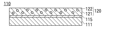
図4の符号110は従来技術の接着フィルムを示している。
接着フィルム110は、PET(ポリエステルテレフタレート)フィルムからなる基材111と、基材111表面に配置された剥離層115と、剥離層115表面に配置された接着剤層120とを有している。
The
この接着フィルム110を用いて接着剤付き基板を製造する工程について説明すると、先ず、基板の貼付面に接着フィルム110の接着剤層120が配置された側の面を押し当て、貼付面と接着剤層120表面とを密着させる。
The process of manufacturing a substrate with an adhesive using the
剥離層115と接着剤層120との間の接着力は、接着剤層120と基板との間の接着力、及び剥離層115と基材111との間の接着力よりも小さくなっており、基材111を基板から剥離すると、剥離層115と接着剤層120の界面で剥離が起こり、剥離層115は基材111と一緒に剥離され、接着剤層120が基板上に残る。
The adhesive force between the
一般に基材111の色は白、透明又はマット状であり、接着剤層120は導電性粒子122が添加されることで黒色か茶色に着色されている。また、剥離層115はシリコーンのような透明な剥離剤で構成されており、従って、接着剤層120が剥離した状態で、基材111の剥離層115が露出した側の面を観察した時に、透明な剥離層115を介して基材111の色が観察されれば、接着剤層120が基材111上に残っていないことを示し、逆に基材111の色が観察されず、接着剤層120の色が観察されれば、接着剤層120が基板に完全に貼付されず、基材111上に残ってしまったことを示す。このように、剥離層115が接着剤層120から露出したときの色を観察することで、接着剤層120の貼付が正常に行われたかどうかを判断することができる。
In general, the color of the
一般に、基材111は絶縁性の樹脂フィルムで構成されており、接着剤層120も絶縁性を有するため、接着フィルム110は上述した貼付の工程等で摩擦により帯電しやすいという問題があった。接着フィルム110が帯電し、帯電した状態の接着剤層120が基板に貼付されてしまうと、基板に他の電気部品を接続した場合に、電気部品の回路や基板の配線膜に悪影響が生じてしまう。
In general, the
例えば、剥離層に第4級アンモニウム塩のようなイオン性導電剤や、金属のような電子伝導剤を添加すれば、剥離層の表面抵抗を小さくなり、接着剤層の帯電を防止することができる。イオン性導電剤は安価で、剥離層の抵抗値を下げる効果も高い。しかしながら、イオン性導電剤は剥離層の表面に染み出すブルームと呼ばれる現象が起こりやすく、ブルームが起こると、基板の配線膜がイオン性導電剤によって腐食されることがある。 For example, if an ionic conductive agent such as a quaternary ammonium salt or an electronic conductive agent such as a metal is added to the release layer, the surface resistance of the release layer can be reduced and charging of the adhesive layer can be prevented. it can. The ionic conductive agent is inexpensive and has a high effect of reducing the resistance value of the release layer. However, the ionic conductive agent tends to cause a phenomenon called “bloom” that oozes out on the surface of the release layer, and when the bloom occurs, the wiring film of the substrate may be corroded by the ionic conductive agent.
また、イオン性導電剤は湿度が高い程抵抗値が低くなる傾向があるので、夏場のように環境湿度が高い時は抵抗値が低く、帯電防止能が高いが、冬場のように環境湿度が低くく、最も帯電防止機能が求められる時には抵抗値が高くなり、帯電防止能が低くなってしまう。 In addition, since the resistance value of ionic conductive agents tends to decrease as the humidity increases, the resistance value is low and the antistatic ability is high when the environmental humidity is high as in summer, but the environmental humidity is low as in winter. When the antistatic function is most demanded, the resistance value becomes high and the antistatic ability becomes low.
電子伝導剤はイオンを含有しないが、剥離層の抵抗値を十分に下げるためには多量に添加する必要がある。電子伝導剤を多量に添加すると、剥離層が電子伝導剤の色に着色されてしまい、接着剤層120の貼付が正常に行われたかどうかの判断が困難になってしまう。
本発明は上記従来技術の不都合を解決するために創作されたものであり、その目的は、帯電防止能を有し、かつ、剥離層が透明な接着フィルムを製造することにある。 The present invention was created to solve the above-mentioned disadvantages of the prior art, and an object of the present invention is to produce an adhesive film having antistatic ability and having a transparent release layer.
上記課題を解決するために請求項1記載の発明は、基材と、前記基材表面に密着配置された剥離層とを有する剥離フィルムと、前記剥離層の表面に密着配置された接着剤層とを有し、前記基材と前記剥離層との間の剥離力は、前記剥離層と前記接着剤層との間の剥離力よりも大きくされた接着フィルムであって、前記剥離層は、剥離剤と、導電性の帯電防止粒子を含有し、前記帯電防止粒子は、透明な金属酸化物であって、インジウム錫酸化物と、錫酸化物と、亜鉛酸化物とからなる群より選択される、少なくとも1種類の金属酸化物を含有し、前記帯電防止粒子の粒径は10nm以上60nm以下にされた接着フィルムである。
請求項2記載の発明は、請求項1記載の接着フィルムであって、前記剥離剤は透明であって、前記接着剤層側から前記接着フィルムの表面を観察したときとの色と、前記接着剤層を除去し、前記剥離層を露出させたときに、前記剥離層の露出する表面を観察したときの色は異なるようにされた接着フィルムである。
請求項3記載の発明は、請求項1又は請求項2のいずれか1項記載の接着フィルムであって、前記基材は白色であって、前記接着剤は白以外の色にされた接着フィルムである。
請求項4記載の発明は、請求項1又は請求項2のいずれか1項記載の接着フィルムであって、前記基材は透明であって、前記接着剤は不透明にされた接着フィルムである。
請求項5記載の発明は、請求項1乃至請求項4のいずれか1項記載の接着フィルムであって、前記帯電防止粒子の粒径は、前記剥離層の膜厚よりも小さくされた接着フィルムである。
請求項6記載の発明は、請求項1乃至請求項5のいずれか1項記載の接着フィルムであって、前記剥離層の膜厚は10nm以上1μm以下にされた接着フィルムである。
請求項7記載の発明は、請求項1乃至請求項6のいずれか1項記載の接着フィルムであって、0.2gの前記剥離フィルムを10mlの水に入れ、加熱温度100℃の条件で10時間放置した後、前記水に溶出するイオン量が15ppm以下になる接着フィルムである。
請求項8記載の発明は、基材と、前記基材表面に配置された剥離層と、前記剥離層の表面に密着配置された接着剤層とを有する接着フィルムの、露出された前記接着剤層表面を基板表面に押し当て、前記接着剤層を前記基板表面に貼付する貼付工程と、前記基材を前記剥離層と一緒に前記接着剤層から剥離する剥離工程とを有する接着剤付き基板の製造方法であって、前記剥離層は透明な剥離剤と、透明な導電性粒子とを含有されたものを用い、前記接着剤層の表面を観察したときの色と、前記基材の前記剥離層と密着する面を観察したときの色である基材色を互いに異なる色にされており、前記剥離工程の後に、前記剥離層表面を検査し、前記剥離層の裏面に密着する前記基材の色が観察された場合に良品と判断する接着剤付き基板の製造方法である。
請求項9記載の発明は、基材と、前記基材表面に配置された剥離層と、前記剥離層の表面に密着配置された接着剤層とを有する接着フィルムの、露出された前記接着剤層表面を基板表面に押し当て、前記接着剤層を前記基板表面に貼付する貼付工程と、前記基材を前記剥離層と一緒に前記接着剤層から剥離する剥離工程とを有する接着剤付き基板の製造方法であって、前記剥離層は透明な剥離剤と、透明な導電性粒子とを含有されたものを用い、前記接着剤層を不透明にしておき、前記剥離工程の後に、前記基材と前記剥離層を透過した光の光量を測定し、測定された前記光量が設定値以上の時には良品と判断する接着剤付き基板の製造方法である。
請求項10記載の発明は、請求項8又は請求項9のいずれか1項記載の接着剤付き基板の製造方法であって、前記基材をローラに接触させながら走行させる接着剤付き基板の製造方法である。
請求項11記載の発明は、帯電防止粒子と、剥離剤を有する塗布組成物を作成し、前記塗布組成物を基材表面に塗布して塗布層を形成した後、前記塗布層を乾燥させて剥離層を形成し、前記剥離層表面に接着剤を塗布して接着剤層を形成する接着フィルムを製造方法であって、前記帯電防止粒子を有機溶媒に分散させて溶媒系スラリーを作成した後、シリコーンを主成分とする剥離剤と、前記溶媒系スラリーとを混合して前記塗布組成物を作成する接着フィルムの製造方法である。
請求項12記載の発明は、請求項11記載の接着フィルムの製造方法であって、前記塗布組成物の塗布は、前記塗布層を乾燥した後の前記剥離層の膜厚が10nm以上1μm以下になるように塗布する接着フィルムの製造方法である。
請求項13記載の発明は、請求項11又は請求項12のいずれか1項記載の接着フィルムの製造方法であって、前記塗布組成物の作成は、前記塗布組成物中の微粉末固形分が1重量%以上10重量%以下になるように、前記溶媒系スラリーを添加する接着フィルムの製造方法である。
In order to solve the above-mentioned problems, the invention according to
Invention of Claim 2 is an adhesive film of
Invention of Claim 3 is an adhesive film of any one of
The invention according to
Invention of
A sixth aspect of the present invention is the adhesive film according to any one of the first to fifth aspects, wherein the release layer has a thickness of 10 nm to 1 μm.
A seventh aspect of the present invention is the adhesive film according to any one of the first to sixth aspects, wherein 0.2 g of the release film is placed in 10 ml of water and heated at a temperature of 100 ° C. After being allowed to stand for a period of time, the adhesive film has an ion amount eluted in the water of 15 ppm or less.
The invention according to claim 8 is the exposed adhesive of an adhesive film having a substrate, a release layer disposed on the surface of the substrate, and an adhesive layer disposed in close contact with the surface of the release layer. A substrate with an adhesive having a bonding step of pressing the surface of the layer against the surface of the substrate and sticking the adhesive layer to the surface of the substrate, and a peeling step of peeling the base material from the adhesive layer together with the peeling layer The release layer comprises a transparent release agent and transparent conductive particles, the color when the surface of the adhesive layer is observed, and the base material The base color which is a color when the surface which adheres to the release layer is observed is made different from each other, and after the release step, the surface of the release layer is inspected and adhered to the back surface of the release layer. Manufacture of substrates with adhesives that are judged to be non-defective when the color of the material is observed It is the law.
The invention according to
Invention of
The invention according to
Invention of
Invention of Claim 13 is a manufacturing method of the adhesive film of any one of
尚、本発明で微粉末固形分とは塗布組成物中に含有される固形分のことであって、具体的には塗布組成物中に含有される帯電防止粒子のことである。 In the present invention, the fine powder solid content is a solid content contained in the coating composition, specifically, an antistatic particle contained in the coating composition.
本発明の接着フィルムは、剥離層に帯電防止粒子が添加されることで、剥離層の表面抵抗が低くなっているので、接着剤層が帯電し難い。また、帯電防止粒子は透明であり、剥離層全体が透明になっているので、接着剤層を剥離した後、露出した剥離層表面から基材の色を観察し、接着剤層の貼付が正常に行われたどうかの判断を行うことができる。また、帯電防止粒子は金属酸化物を主成分とするので、金属粒子に比べて溶媒に対する親和性が高い。従って、接着剤層を形成するために、溶媒を含有した接着剤を塗布したときに接着剤のはじきが発生せず、膜厚均一な接着剤層を形成することができる。 In the adhesive film of the present invention, the antistatic particles are added to the release layer, so that the surface resistance of the release layer is low, so that the adhesive layer is difficult to be charged. In addition, since the antistatic particles are transparent and the entire release layer is transparent, after peeling off the adhesive layer, the color of the substrate is observed from the exposed release layer surface, and the adhesive layer is normally applied. Judgment can be made as to whether or not In addition, since the antistatic particles contain a metal oxide as a main component, they have a higher affinity for the solvent than the metal particles. Therefore, when an adhesive containing a solvent is applied to form the adhesive layer, the adhesive does not repel, and an adhesive layer having a uniform film thickness can be formed.
本発明の接着フィルムを製造する工程の一例について説明する。
先ず、粒径が10nm以上60nm以下の帯電防止粒子と、有機溶媒とを混合し、溶媒系スラリーを作成する。次に、溶媒系スラリーと、透明なシリコーンからなる液状の剥離剤と、該剥離剤の架橋反応を促進する硬化剤とを混合し、液状の塗布組成物を作成する。
An example of the process for producing the adhesive film of the present invention will be described.
First, an antistatic particle having a particle size of 10 nm to 60 nm and an organic solvent are mixed to prepare a solvent-based slurry. Next, a solvent-based slurry, a liquid release agent made of transparent silicone, and a curing agent that promotes a crosslinking reaction of the release agent are mixed to prepare a liquid coating composition.
帯電防止粒子の粒径が10nm以上60nm以下と小さい場合には剥離剤に対する分散性が低いため、帯電防止粒子と剥離剤とを直接混合すると帯電防止粒子が沈殿しやすいが、本発明では予め帯電防止粒子と有機溶媒とを混合して溶媒系スラリーを作成することで、剥離剤に対する帯電防止粒子の分散性が向上しているので、帯電防止粒子を分散させる分散剤を用いずに、塗布組成物中で帯電防止粒子を分散させることができる。 When the particle size of the antistatic particles is as small as 10 nm or more and 60 nm or less, the dispersibility with respect to the release agent is low. Therefore, when the antistatic particles and the release agent are mixed directly, the antistatic particles are likely to precipitate. Dispersion of antistatic particles in the release agent is improved by mixing solvent particles with an organic solvent to create a solvent slurry, so that the coating composition can be used without using a dispersant that disperses the antistatic particles. Antistatic particles can be dispersed in the product.
次いで、該塗布組成物を、グラビアコータ等の塗布手段を用い、加熱乾燥後の膜厚が10nm以上1μm以下になるように第一の基材表面に塗布し、塗布層を形成する。 Next, the coating composition is coated on the surface of the first substrate using a coating means such as a gravure coater so that the film thickness after heat drying is 10 nm or more and 1 μm or less to form a coating layer.
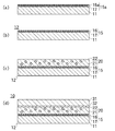
図1(a)は第一の基材11表面に塗布層15aが形成された状態を示す断面図である。上述したように、帯電防止粒子17は塗布組成物中で分散しているので、塗布直後は、塗布層15a中の帯電防止粒子17の分布は均一になっているが、帯電防止粒子17はITO(インジウム・錫酸化物)で構成されており、その比重は剥離剤16aよりも高いので、帯電防止粒子17は塗布後には塗布層15a内部で沈殿する。従って、帯電防止粒子17は塗布層15aの表面からの深さが深さが深い方が多く分布するが、その平面分布は均一になっている。
FIG. 1A is a cross-sectional view showing a state in which a coating layer 15 a is formed on the surface of the
帯電防止粒子17の平均粒径は、塗布層15aの膜厚よりも小さくなっているので、帯電防止粒子17の表面は塗布層15aから露出せず、剥離剤16aで覆われた状態になっている。次いで、塗布層15aを剥離剤16aが架橋する架橋温度以上に加熱し、乾燥すると余分な有機溶媒が蒸発すると共に、剥離剤16aの架橋反応が起こる。
Since the average particle size of the
塗布層15aに帯電防止剤として第4級アンモニウム塩のようなイオン性導電剤が添加されていると、該導電剤が触媒毒として作用し、剥離剤16aの架橋反応が阻害されるが、上述したように帯電防止粒子17は金属酸化物で構成されており、イオン導電剤を含有しないので、剥離剤16aの架橋反応が阻害されずに進行し、剥離剤16aが帯電防止粒子17の表面を覆った状態で硬化し、第一の剥離層が形成される。
When an ionic conductive agent such as a quaternary ammonium salt is added to the coating layer 15a as an antistatic agent, the conductive agent acts as a catalyst poison and inhibits the crosslinking reaction of the release agent 16a. As described above, since the
図1(b)は第一の剥離層15が形成された状態の剥離フィルム12を示す断面図である。図1(b)の符号16は硬化した剥離剤を示しており、上述したように剥離剤は帯電防止粒子17の表面を覆った状態で硬化し、硬化する前の塗布層15aと硬化した後の第一の剥離層15の膜厚は変化しないので、帯電防止粒子17は第一の剥離層15から露出しない。
FIG. 1B is a cross-sectional view showing the
次に、熱硬化性樹脂からなるバインダー樹脂と、金属粒子からなる導電性粒子と、溶媒とを混合、分散して液状の接着剤を作成し、この接着剤を第一の剥離層15上に塗布すると、接着剤中の溶媒の一部が第一の剥離層15の表面から内部に浸透する。
Next, a binder resin made of a thermosetting resin, conductive particles made of metal particles, and a solvent are mixed and dispersed to prepare a liquid adhesive, and this adhesive is applied to the
上述したように帯電防止粒子17は第一の剥離層15から露出しておらず、接着剤と帯電防止粒子17は直接接触しないが、本願では剥離層15の膜厚が10nm以上1μmであるのに対し、帯電防止粒子17の粒径は10nm以上60nm以下の範囲であり、帯電防止粒子17を覆う剥離剤16の厚さが最大で240nmと小さいので、第一の剥離層15に浸透した溶媒は帯電防止粒子17に到達する。
As described above, the
上述したように帯電防止粒子17は金属酸化物で構成されており、接着剤に用いられる溶媒は、金属単体に対する親和性よりも金属酸化物に対する親和性が高いので、溶媒は帯電防止粒子17に弾かれず、一部が帯電防止粒子17に浸透する。従って、この第一の剥離層15では接着剤中の溶媒が弾かれることがなく、結果として接着剤と第一の剥離層15との親和性が高くなるので、接着剤が第一の剥離層15で弾かれることがなく、第一の剥離層15表面に均一に接着剤が塗布される。接着剤を塗布後、全体を乾燥させて、接着剤から余分な溶媒を蒸発、除去すると、第一の剥離層15表面に接着剤層が形成される。
As described above, the
図1(c)は接着剤層20が形成された状態を示しており、この接着剤層20はバインダー樹脂21中に導電性粒子22が分散された状態になっている。次いで、表面に第二の剥離層32が形成された第二の基材31を用意し、第二の剥離層32を接着剤層20に向けた状態で、第二の剥離層32と一緒に第2の基材31を接着剤層20に押し当てると、図1(d)に示すような本発明の接着フィルム10が得られる。
FIG. 1C shows a state where an
ここでは、第一の基材11は長尺形状であって、第一の基材11上に形成された剥離層15と接着剤層20も第一の基材11と同じ長尺形状になっている。また、第二の基材31は第一の基材11と同じ長尺形状にされており、従ってこの接着フィルム10全体の形状は長尺になっている。
Here, the
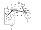
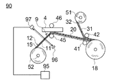
図2は基板4に接着剤層20を貼付する工程を説明するための図面である。図2の符号1は接着剤層20の貼付に用いられる貼付装置を示しており、この貼付装置1は第一、第二の押圧ローラ45、46と、第一、第二の剥離ローラ41、42とを有している。この貼付装置1を用いて接着剤付き基板を製造するには、先ず、上述した接着フィルム10のロール18を形成する。
FIG. 2 is a drawing for explaining a process of attaching the
図2は基板4に接着剤層20を貼付するときの状態を示しており、この状態では接着フィルム10はロール18から引き出されて第一、第二の剥離ローラ41、42の間を通った後、第二の基材31が巻き取り軸51に巻き取られ、第一の基材11が第一、第二の押圧ローラ45、46の間を通った後、巻き取り軸52に巻き取られている。
FIG. 2 shows a state when the
第二の剥離層32は第一の剥離層15とは異なる剥離剤で構成されており、その剥離剤の選択により、第二の剥離層32と接着剤層20との間の接着力は、第二の基材31と第二の剥離層32との間の接着力と、第一の剥離層15と接着剤層20との間の接着力と、第一の剥離層15と第一の基材11との間の接着力のいずれの接着力よりも弱くされている。
The
従って、第一、第二の基材11、31を巻き取り軸51、52で巻き取り、第一、第二の基材11、31を走行させながら、第一、第二の剥離ローラ41、42で第一、第二の基材11、31の走行方向を変えると、接着力の相違により、第二の剥離層32と接着剤層20との界面で剥離が起こって接着剤層20が露出し、第二の剥離層32は第二の基材31と一緒に巻き取られ、露出した接着剤層20は第一の基材11と一緒に第一、第二の押圧ローラ45、46の間に向かって走行する。
Accordingly, the first and
基板4は接着剤を貼付すべき貼付面が第一の基材11に向けられた状態で、第一、第二の押圧ローラ45、46の間に配置されている。第一の基材11の基板4と対向する面とは反対側の面を観察できる位置、ここでは、第一の基材11上の位置には第一の観察手段6が配置されている。第一の観察手段6と、後述する第二の観察手段7はそれぞれ制御装置5に接続され、第一、第二の観察手段6、7から送られる信号によって制御装置5が第一、第二の観察手段6、7が観察する色を判断するようになっている。
The
第一の基材11は、基材を構成するPET樹脂に着色剤が添加されることによって白色になっているのに対し、接着剤層20は有色の導電性粒子22が添加されることで第一の基材11とは異なる色(例えば黒色、茶色)に着色されており、接着剤層20が基板4に向けられた状態で第一の基材11が走行する場合には、制御装置5が第一の基材11の色である白色を観察するが、第一の基材11にねじれや切断が生じた場合には、接着剤層20の色や背景色等、第一の基材11とは異なる色を観察するようになる。
The
制御装置5は第一の観察手段6から送られる信号によって白色を観察している時は「正常」と判断し第一の基材11の走行を続けるが、白色以外の色を観察する時には「異常」と判断し、第一の基材11の走行を停止させる。このように、第一の基材11を第一、第二の押圧ローラ45、46の間に送り、後述する貼付工程を行う前に、接着剤層20が基板4と対向しているかどうかの検査を行うことで、貼付工程の際には必ず接着剤層20が基板4の対向するようになっている。
The
第一の基材11は第一の押圧ローラ45に支持された状態で走行しており、接着剤層20が基板4の貼付面と対向する位置に位置した時に、第一の押圧ローラ45を移動させ、第一、第二の押圧ローラ45、46間の距離を縮めると、第一の基材11が基板4に押し付けられ、接着剤層20が基板4の貼付面と密着し、接着剤層20が基板4に貼付される(貼付工程)。
The
剥離剤16の選択により、第一の剥離層15と接着剤層20との間の接着力は、第一の剥離層15と第一の基材11の間、及び第一の接着剤層20と基板4との間の接着力よりも小さくされている。帯電防止粒子17が接着剤層20と直接接触すると、第一の剥離層15の接着力が大きくなってしまうが、上述したように帯電防止粒子17は剥離剤16で覆われているため、第一の剥離層15の接着力は大きくならず、従って、第一の押圧ローラ45を第二の押圧ローラ46から離し、第一の基材11が基板4から離れると、第一の剥離層15も第一の基材11と一緒に剥離され、接着剤層20が基板4上に残る(剥離工程)。
Depending on the selection of the
第一の基材11が剥離された後、切断手段9によって接着剤層20を基板4上で切断し、接着剤層20のうち、貼付面に貼付された部分を、他の部分から分離すれば、後述する接着剤付き基板が得られる。
After the
少なくとも、貼付工程と、剥離工程と、第二の基材31を剥離する工程では、第一の押圧ローラ45又は第一の剥離ローラ41が第一の基材11に接触しており、貼付工程と剥離工程では第一の基材11は第一の押圧ローラ45に接触した状態で走行し、第二の基材31を剥離する工程では第一の基材11は第一の剥離ローラ41に接触した状態で走行する。第一の基材11は絶縁性の樹脂で構成されているため、第一の基材11がそれらのローラ41、45に接触した状態で走行すると摩擦により第一の基材11が帯電する。
At least in the sticking step, the peeling step, and the step of peeling the
本発明の接着フィルム10は、上述したように第一の剥離層15に帯電防止粒子17が添加されており、第一の剥離層15は導電性を有する程度に表面抵抗が小さくなっている。従って、第一の基材11が帯電したとしても、その電気は第一の剥離層15でリークされるので接着剤層20が帯電せず、基板4に貼付される接着剤層20の帯電量が従来よりも小さくなる。
In the
第一の基材11は接着剤層20が剥離された後、第一の剥離層15が露出した状態で巻き取り軸に向かって走行する。露出した第一の剥離層15の表面を観察できる位置、ここでは第一の剥離層15上には第二の観察手段7が配置されている。
After the
第一の剥離層15には透明は剥離剤16が用いられ、また帯電防止粒子17にも透明な金属酸化物が用いられており、第一の剥離層15全体が透明になっているので、第一の剥離層15が露出した状態では、透明な第一の剥離層15の表面側から裏面側に位置する第一の基材11の色が観察される。
Since the
第二の観察手段7が観察する色が第一の基材11の色である時には、制御装置5は「正常」と判断するが、接着剤層20が第一の剥離層15上に残り、第二の観察手段7が観察する色が第一の基材11の色以外の色である時には、制御装置5は「不良」と判断し、対応する接着剤付き基板4に「不良」を示すマーキングをする。マーキングされた接着剤付き基板4は次の工程に送られる前に取り除かれるので、電気部品を接続する工程での歩留りが向上する。
When the color observed by the second observation means 7 is the color of the
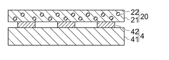
図3は接着剤付き基板4を示す断面図である。ここでは、基板4はLCD(Liquid Crystal Display)のような表示装置に用いられるガラス基板で構成されている。この基板4はガラス板41と、ガラス板41上に形成された配線膜42とを有しており、配線膜42が配置された部分で貼付面が構成され、該貼付面に接着剤層20が配置されている。
FIG. 3 is a sectional view showing the
半導体素子等の他の電気部品の接続端子が配置された側の面を接着剤層20に押し当て加熱押圧すれば、バインダー樹脂21が加熱によって軟化し、電気部品の接続端子が軟化したバインダー樹脂21を押し退け、該接続端子と配線膜42とで導電性粒子22が挟み込まれる。更に押圧を続けるとバインダー樹脂21が硬化され、基板4と電気部品とが硬化したバインダー樹脂21によって機械的に接続され、導電性粒子22によって電気的にも接続された電気装置が得られる。
If the surface on which the connection terminals of other electrical components such as semiconductor elements are arranged is pressed against the
接着剤層20が帯電していると、電気部品の回路に悪影響を生じる場合があるが、上述したように本発明では接着剤層20の帯電は第一の剥離層15によって防止されるので、信頼性の高い電気装置が得られる。
If the
以上は帯電防止粒子17をITOで構成する場合について説明したが、本発明はこれに限定されるものではなく、透明で、かつ、導電性を有する金属酸化物であれば、例えば、亜鉛酸化物、錫酸化物を用いることもできる。また、これらの金属酸化物の粒子を2種類以上1つの剥離層15(第一の剥離層)に添加することもできる。
The above is a description of the case where the
第一の剥離層15の膜厚が厚くなると、接着フィルム10の生産性が落ちるなど不具合が多くなる。従って第一の剥離層15の膜厚は薄い方が好ましく、本発明に適した膜厚の範囲は10nm以上1μm以下、より好ましくは30nm以上300nm以下である。
When the thickness of the
帯電防止粒子17が第一の剥離層15から露出すると第一の剥離層15の接着力が強くなりすぎるので、帯電防止粒子17を露出させないためには、その粒径は第一の剥離層15の膜厚以下である好ましく、より好ましくは10nm以上60nm以下である。
When the
帯電防止粒子17の粒径が、第一の剥離層15の膜厚と略等しい場合には、帯電防止粒子17が存在せず、剥離剤16だけが位置する部分の膜厚が、帯電防止粒子17の粒径よりも小さくなることがあるが、その場合であっても、帯電防止粒子17は剥離剤16で覆われるので、接着剤層20と帯電防止粒子17とが直接接触することはない。
When the particle size of the
以上は、第一の基材11に白色の着色剤が添加され、白色に着色された場合について説明したが、本発明はこれに限定されるものではなく、例えば基材12を構成する樹脂の結晶性によって白濁し、不透明又は半透明になったマット状のものを用いることもできる。また、第一の基材11の色は接着剤層20と異なる色であれば白色に限定されるものではない。
The above describes the case where a white colorant is added to the
また、第一の基材11全体を着色する必要もない。例えば、第一の基材11の第一の剥離層15が形成される側の面に、有色であって、接着剤層20とは異なる色の図形や文字を印刷しておけば、第二の観察手段7によってその図形や文字の色を観察することができる。
Further, it is not necessary to color the entire
第一の基材11構成する樹脂もPET樹脂に限定されず、PET樹脂以外のポリエチレン樹脂、ポリプロピレン樹脂、ポリアクリル樹脂等種々のものを用いることができる。
The resin constituting the
剥離剤に用いるシリコーンは加熱によって硬化する加熱硬化型に限定されず、紫外線照射によって硬化する紫外線硬化型のものも用いることができる。また、剥離剤はシリコーンに限定されるものではない。 The silicone used for the release agent is not limited to a heat-curing type that is cured by heating, and an ultraviolet curing type that is cured by ultraviolet irradiation can also be used. Further, the release agent is not limited to silicone.
以上は接着剤層20に用いられるバインダー樹脂がエポキシ樹脂である場合について説明したが、本発明はこれに限定されるものではなく、アクリル樹脂、イソシアネート樹等他の熱硬化性樹脂や、これらの熱硬化性樹脂と、エポキシ樹脂のうち、2種類以上の熱硬化性樹脂を混合して用いることも可能である。
As described above, the case where the binder resin used for the
また、熱硬化性樹脂の他に、バインダー樹脂にフェノキシ樹脂等の熱可塑性樹脂や、熱硬化性樹脂を硬化させる硬化剤や、着色剤や老化防止剤のような添加剤を添加することもできる。 In addition to the thermosetting resin, a binder resin such as a thermoplastic resin such as a phenoxy resin, a curing agent that cures the thermosetting resin, or an additive such as a colorant or an antioxidant can be added. .
導電性粒子22も特に限定されるものではなく、樹脂粒子の表面に金属メッキ層が形成された導電層付き樹脂粒子や、金属粒子単体を用いることができる。導電性粒子22の色は多くは茶色か黒色であるが、特に限定されるものではない。また、バインダー樹脂21に着色剤を添加することで、接着剤層20の色を基材11とは異なる色に変えることも可能である。
The
基板4もガラス基板に限定されず、ガラスエポキシ板やセラミック板上に配線膜が形成されたリジッド基板や、樹脂フィルム上に配線膜が形成されたフレキシブル配線板を用いることもできる。また、基板4に接続される電気部品も半導体素子に限定されず、他の配線板や電気装置等種々のものを接続することができる。
The
以上は、長尺状の接着フィルム10を走行させ、接着剤層20を基板4に貼付させてから接着剤層20の切断を行う場合について説明したが、本発明はこれに限定されるものではない。予め、接着フィルム10を基板4の貼付面と略等しい平面形状に切断してフィルム片を作成し、該フィルム片を接着剤付き基板の製造に用いれば、貼付工程と剥離工程の後で接着剤層20を切断する必要がない。
The above has described the case where the
<実施例1〜7>
有機溶媒と帯電防止粒子とからなる溶媒系スラリーと、剥離剤と、硬化触媒とを、下記表1に示す配合比率(重量)で配合し、帯電防止粒子が凝集せず、その粒径が10nm以上60nm以下に維持されるように混合し、分散剤を含有しない剥離剤用の塗布組成物を3種類作成した。ここでは、有機溶媒としてトルエンとメチルエチルケトンの混合溶媒(重量比1:1)を用いた。次いでその塗布組成物をPETフィルムからなる基材11の表面に#6コイルバーを用いて塗布して塗布層15aを形成した後、160℃、1分の条件で乾燥させ、剥離剤16aを硬化させて剥離層15を形成し、実施例1〜7の剥離フィルム12を作成した。塗布組成物の組成を下記表1に示す。
<Examples 1-7>
A solvent-based slurry composed of an organic solvent and antistatic particles, a release agent, and a curing catalyst are blended at a blending ratio (weight) shown in Table 1 below, and the antistatic particles do not aggregate, and the particle size is 10 nm. Three types of coating compositions for a release agent that did not contain a dispersant were mixed so as to be maintained at 60 nm or less. Here, a mixed solvent of toluene and methyl ethyl ketone (weight ratio 1: 1) was used as the organic solvent. Next, the coating composition is applied to the surface of the

尚、上記表1中の数字は重量部を示す。ここでは、剥離剤として、信越化学工業(株)社製の商品名「KS847」(シリコーン濃度30重量%)、「KS830」(シリコーン濃度30重量%)を用い、硬化触媒としては信越化学工業(株)社製の商品名「PL50T」を用い、溶媒系スラリーとしてはシーアイ化成(株)社製の商品名「ナノテックITOエタノールスラリー」と、(株)ソルベックス社製の商品名「マイクロソルバーLIT−41A」を用いた。 In addition, the number in the said Table 1 shows a weight part. Here, trade names “KS847” (silicone concentration 30% by weight) and “KS830” (silicone concentration 30% by weight) manufactured by Shin-Etsu Chemical Co., Ltd. are used as the release agent, and Shin-Etsu Chemical ( The product name “PL50T” manufactured by Co., Ltd. is used, and as the solvent-based slurry, the product name “Nanotech ITO ethanol slurry” manufactured by CI Chemical Co., Ltd. 41A "was used.
「ナノテックITOエタノールスラリー」と、「マイクロソルバーLIT−41A」はそれぞれITO微粒子を溶媒に分散させた縣濁液(溶媒系スラリー)であり、ITO粒子の濃度(重量%)は「ナノテックITOエタノールスラリー」が35重量%、「マイクロソルバーLIT−41A」が30重量%である。尚、「ナノテックITOエタノールスラリー」に含有されるITO粒子は90%以上の粒径が20.8nm未満の範囲にあり、その平均粒径は16.4nmである。 “Nanotech ITO ethanol slurry” and “Microsolver LIT-41A” are suspensions (solvent slurry) in which ITO fine particles are dispersed in a solvent, respectively. The concentration (% by weight) of ITO particles is “Nanotech ITO ethanol slurry”. "Is 35 wt% and" Microsolver LIT-41A "is 30 wt%. The ITO particles contained in the “Nanotech ITO ethanol slurry” have a particle size of 90% or more in the range of less than 20.8 nm, and the average particle size is 16.4 nm.
<比較例1、2>
上記表1に記載された配合比率で、剥離剤と、有機溶媒と、硬化触媒とを混合し、帯電防止粒子を含有しない塗布組成物を2種類作成し、これらの塗布組成物を用いて、実施例1〜7と同じ条件で剥離層を形成し、比較例1、2の剥離フィルムを作成した。上記実施例1〜7、比較例1、2の剥離フィルムを用いて下記に示す「剥離力」、「残留接着率」、「抵抗値」、「イオン含有率」の各評価試験を行った。
<Comparative Examples 1 and 2>
Mixing a release agent, an organic solvent, and a curing catalyst at the mixing ratio shown in Table 1 above, creating two types of coating compositions that do not contain antistatic particles, and using these coating compositions, A release layer was formed under the same conditions as in Examples 1 to 7, and release films of Comparative Examples 1 and 2 were prepared. Each evaluation test of “peeling force”, “residual adhesion rate”, “resistance value”, and “ion content rate” shown below was performed using the release films of Examples 1 to 7 and Comparative Examples 1 and 2.
〔剥離力〕
剥離フィルムの剥離層15が形成された面を貼着対象物に密着し、70℃の温度条件で20時間圧着した後、剥離フィルムを貼着対象物から剥離するときに要した力(剥離力)を測定した。尚、剥離フィルム12として実用上に必要な剥離力は0.5N/cm以上である。
[Peeling force]
The force (peeling force) required when the release film was peeled from the object to be adhered after the surface of the release film on which the
〔残留接着率〕
上記「剥離力」試験で剥離力を測定後、剥離フィルム12の剥離層15表面にPETフィルムを貼付した後、剥離フィルム12をPETフィルムから剥がすときの剥離力を測定し、測定剥離力とした。これとは別に標準となる剥離テープ(標準テープ)と新たなPETフィルムとを貼付後、剥離する時の力を標準剥離力とし、測定剥離力÷標準剥離力×100で算出される値を残留接着率(%)とした。尚、残留接着率の値が小さい程、剥離テープの劣化が激しいことを示しており、剥離フィルムとして実用上に必要な残留接着率は80%以上である。
[Residual adhesion rate]
After measuring the peeling force in the “peeling force” test, after sticking a PET film to the surface of the
〔抵抗値〕
剥離フィルム12を10cm角程度の大きさに切り取って試料片とし、該試料片の表面抵抗をヒューレット・パッカード社製の高抵抗計で測定した。尚、表面抵抗の値が1011Ω未満であれば接着フィルムに用いた時に、十分な帯電防止効果が得られる。
〔Resistance values〕
The
〔イオン含有率〕
剥離フィルム12を細かく切断後、0.2gを精秤し、10mlの超純水と一緒に容器に入れ、100℃のオーブン内に10時間放置した。この超純水に溶出したイオン量を測定した。これとは別にブランクとして超純水のイオン量を測定し、ブランクのイオン量との比をイオン含有率とした。
[Ion content]
After the
〔印字性〕
剥離フィルム12の剥離層15が形成された側の面に油性の速乾性インクで文字を書き、インクの弾かれ具合を観察した。インクの弾きが観察されなかったものを「5」、小さい点状のハジキが観察されたものを「4」、小円状のハジキが観察されたものを「3」、字が点々状になったものを「2」、字がかすれてしまったものを「1」として評価した。
(Printability)
Letters were written with oily quick-drying ink on the surface of the
本発明に用いる接着剤は、速乾性インクと同様に有機溶媒を含有しているため、この印字性試験の評価が高ければ、接着剤の塗布性が高いことを示しており、特に評価が「3」以上であれば接着剤を塗布したときの塗布膜の厚さが均一になる。各評価試験の結果を下記表2に記載する。 Since the adhesive used in the present invention contains an organic solvent in the same manner as the quick-drying ink, if the evaluation of this printability test is high, it indicates that the applicability of the adhesive is high. If it is 3 ”or more, the thickness of the coating film when the adhesive is applied becomes uniform. The results of each evaluation test are shown in Table 2 below.
上記表2から明らかなように、実施例1〜7、比較例1、2の剥離フィルム12は残留接着率が高く、剥離フィルム12の剥離力が高温保存後も変化し難いことがわかる。また、各剥離フィルム12のイオン含有率は実用上十分に低かった
実施例1〜7の抵抗値は2×10⁸Ωと実用上十分に低かったのに対し、比較例1、2の剥離フィルムの抵抗値は、高抵抗計の測定範囲を超える程に高く、絶縁性が非常に高いことが確認された。従って、実施例1〜7の剥離フィルム12を接着フィルムに用いた場合には帯電防止効果が期待できるが、帯電防止粒子を含有しない比較例1、2の剥離フィルムは帯電防止効果が得られないと推測される。
As is clear from Table 2 above, it can be seen that the
また、実施例1〜7のうち、溶媒系スラリーの添加量が3重量部以上であった実施例1〜5は印字性が「3」を超えていたが、溶媒系スラリーの添加量が3重量部未満であった実施例6、7は印字性の評価が低かった。このことから、塗布組成物100重量部中の溶媒系スラリーの添加量が3重量部以上であれば、接着剤の塗布性が特に高くなることがわかる。 In Examples 1 to 7, Examples 1 to 5 in which the addition amount of the solvent-based slurry was 3 parts by weight or more had printability exceeding “3”, but the addition amount of the solvent-based slurry was 3 In Examples 6 and 7 which were less than parts by weight, the evaluation of printability was low. From this, it can be seen that when the addition amount of the solvent-based slurry in 100 parts by weight of the coating composition is 3 parts by weight or more, the applicability of the adhesive is particularly improved.
例えば、剥離剤にセルロースを添加して剥離フィルムの剥離層を形成することは公知であり、セルロースを添加すれば印字性は向上するが、セルロースは接着剤中の有機溶媒に溶解、膨潤する性質を有しているので、セルロースが溶解、膨潤した部分で剥離層と接着層との接着力が非常に高くなり、接着層が剥離層から剥離されないことがある。 For example, it is known that cellulose is added to a release agent to form a release layer of a release film. When cellulose is added, printability is improved, but cellulose is dissolved and swollen in an organic solvent in an adhesive. Therefore, the adhesive force between the release layer and the adhesive layer becomes very high at the part where the cellulose is dissolved and swollen, and the adhesive layer may not be peeled from the release layer.
本発明では、剥離層にセルロースを添加しなくても、帯電防止粒子によって印字性が向上している上に、帯電防止粒子は有機溶媒に溶解、膨潤しないので、剥離フィルムの剥離性を維持しながら、印字性を高くすることができる。 In the present invention, the printability is improved by the antistatic particles without adding cellulose to the release layer, and the antistatic particles do not dissolve or swell in the organic solvent, so that the peelability of the release film is maintained. However, the printability can be improved.
更に、実施例1と同じ剥離剤と帯電防止粒子とを用いて塗布組成物を作成し、この塗布組成物を用いて白色のPETフィルムからなる基材上に膜厚50μmの剥離層を形成して実施例8の剥離フィルム12を作成した。
Furthermore, a coating composition was prepared using the same release agent and antistatic particles as in Example 1, and a 50 μm-thick release layer was formed on a substrate made of a white PET film using this coating composition. A
この実施例8の剥離フィルム12と、塗布組成物を塗布する前の白色PETフィルム(膜厚50μm)と、透明PETフィルム(膜厚25μm)と、従来品の剥離フィルムについて、上記「イオン含有率」と同じ条件で超純水に溶出したイオン量(ppm)を測定した。その結果を下記表3に記載する。
About the
尚、上記表3の商品名「065AD」はソニーケミカル(株)社製の剥離フィルム(膜厚:50μm、基材:白色PET)であり、剥離層には帯電防止剤としてポリチオフェンが添加されている。商品名「400A」はソニーケミカル(株)社製の剥離フィルム(膜厚:50μm、基材:白色PET)であり、剥離層には帯電防止剤としてイオン伝導剤が添加されている。 The trade name “065AD” in Table 3 above is a release film (film thickness: 50 μm, base material: white PET) manufactured by Sony Chemical Co., Ltd., and polythiophene is added to the release layer as an antistatic agent. Yes. The trade name “400A” is a release film (film thickness: 50 μm, base material: white PET) manufactured by Sony Chemicals Corporation, and an ion conductive agent is added to the release layer as an antistatic agent.
上記表3から明らかなように、実施例8の剥離フィルム12は、基材として用いられる白色PETフィルムとイオン量合計がほぼ同じであり、従って、剥離層単体では殆どイオンを含有していないことがわかる。これに対し、従来品の剥離フィルムはイオン量合計が非常に高くなっている。
As is clear from Table 3 above, the
一般に、上述した条件で測定されるイオン含有量が15ppm以下の範囲にあれば電気部品を接続した際に、回路パターンの腐食が起こりにくいとされている。従って、本発明の剥離フィルム12を用いれば、従来の剥離フィルムを用いた場合に比べ基板4に転着した接着剤層20にイオンが付着し難く、接着剤層20を介して基板4に電気部品を接続した場合に、電気部品の回路パターンが腐食され難い。
In general, if the ion content measured under the above-described conditions is in the range of 15 ppm or less, it is said that corrosion of the circuit pattern does not easily occur when an electrical component is connected. Therefore, when the
また、ITO粒子に変え、銅マイクロ粒子(三井金属鉱業(株)社製の銅微粉末、一次粒径1μm)と、カーボンブラック(日本イーシー社製のケッチェンブラック、一次粒径30nm)を用い、各帯電防止粒子と、剥離剤(信越化学工業(株)社製の商品名「KS847」)とを混合して塗布組成物を作成し、剥離層を形成したところ、銅マイクロ粒子を用いた場合には、その含有量が塗布組成物全体の30重量%以上にした場合には、十分な帯電防止効果が得られるが、剥離力、残留接着率共に実用上十分ではなかった。
Also, instead of ITO particles, copper microparticles (copper fine powder manufactured by Mitsui Mining & Smelting Co., Ltd.,
また、カーボンブラックを微粉末のまま塗布組成物に添加した場合には抵抗値と剥離力が高く、剥離フィルムとしては不適切であった。カーボンブラックをシリコーン剥離剤と混練りした後、塗布組成物に用いた場合には、カーボンブラックの添加量が9重量%以上にした場合に抵抗値が低くなり、十分な帯電防止効果が得られたが、残留接着率の値が不十分であった。また、カーボンブラックを用いた場合も銅マイクロ粒子を用いた場合も、剥離層全体がそれらの粒子によって着色されるため、剥離層の基材とは反対側の面から基材の色を観察することができなかった。従って、金属粒子やカーボンブラック粒子は、上述した接着フィルムの帯電防止粒子には不適切であることがわかる。 In addition, when carbon black was added to the coating composition as a fine powder, the resistance value and the peeling force were high, which was inappropriate as a release film. When carbon black is kneaded with a silicone release agent and then used in a coating composition, the resistance value decreases when the amount of carbon black added is 9% by weight or more, and a sufficient antistatic effect is obtained. However, the value of the residual adhesion rate was insufficient. In addition, when using carbon black or copper microparticles, the entire release layer is colored by these particles, so the color of the substrate is observed from the surface of the release layer opposite to the substrate. I couldn't. Therefore, it can be seen that metal particles and carbon black particles are inappropriate for the antistatic particles of the adhesive film described above.
以上は、接着剤層20を剥離した後の色を観察し、「正常」か「不良」かを判断する場合について説明したが、本発明はこれに限定されるものではない。
図5の符号90は本発明に用いられる貼付装置の他の例を示している。この貼付装置90は、上述した第一、第二の観察手段6、7の代わりに、反射手段96と観察手段97を有する以外は、上記図2に示した貼付装置1と同じ構成を有している。
The above has described the case where the color after the
The code |
観察手段97は剥離工程直後の剥離フィルム12上に配置され、反射手段96は剥離フィルム122を挟んで観察手段97と反対側に配置されている。観察手段97は発光部と受光部とを有しており、発光部は所定波長の光(例えば赤外線)を剥離フィルム12に向かって照射する。
The
第一の基材11は透明な樹脂フィルムで構成されており、図1(a)〜(d)で示したように、第一の剥離層15は透明な帯電防止粒子が添加されることで透明にされているので、剥離フィルム12全体が透明になっている。
The
接着剤層20が基板4に転着され、剥離工程後の第一の剥離層15上に接着剤層20が残留していない時には、発光部からの光は透明な第一の剥離層15と、透明な第一の基材11とを透過し、剥離フィルム12の反対側に位置する反射部材96に到達すると、該反射部材96で観察手段97側へ反射され、その反射光が第一の基材11と、第一の剥離層15とを再び透過して観察手段97へ戻り、観察手段97の受光部に入射する。
When the
受光部に反射光が入射すると、観察手段97はその反射光を電気信号に変えて制御装置95へ出力し、制御装置95はその電気信号を光量に変換する。ここでは、接着剤層20は不透明にされており、剥離工程で接着剤層20が基板4に転着されず、第一の剥離層15表面に残ると、発光部から照射される光は接着剤層20で吸収されるので、受光部に入射する光量が非常に少なくなる。
When the reflected light is incident on the light receiving unit, the
反射手段96で光が反射された時に制御装置95が検出する光量と、接着剤層20で光が吸収された時に制御装置95が検出する光量の間の値を設定値として制御装置95に入力しておき、検出される光量が設定値以上のときは「正常」と判断し、設定値未満のときは「不良」と判断するように制御装置95を設定しておく。
A value between the light amount detected by the
制御装置95が「不良」と判断したときに、対応する接着剤付き基板4に「不良」を示すマーキングをするようにすれば、マーキングされた接着剤付き基板4を次の工程に送る前に容易に取り除くことができる。
If the
以上は、観察手段97の発光部から照射された光が反射部材96で反射した反射光を検出する場合について説明したが、本発明はこれに限定されるものではない。例えば、剥離フィルム12を挟んで観察手段97と反対側に、所定波長の光を放出する発光装置を配置し、該発光装置から放出され、剥離フィルム12を透過した透過光を観察手段の受光部に入射させてもよい。
Although the case where the light irradiated from the light emitting part of the
この場合、接着剤層20が第一の剥離層15上に残らず、剥離フィルム12を透過した光が接着剤層20に吸収されなかった場合に観察手段97で検出される光量と、剥離フィルム12を透過した光が接着剤層20で吸収された場合に検出される光量との間の値を設定値として制御装置95に入力しておけば、上述した貼付装置90の場合と同様に、制御装置95に接着剤付き基板4が「正常」か「不良」かを判断させることができる。
In this case, the amount of light detected by the observation means 97 when the
1、90……貼付装置 4……基板 6、7……観察手段 10……接着フィルム 11……基材(第一の基材) 12……剥離フィルム 15……剥離層 16……剥離剤 17……帯電防止粒子 20……接着剤層 21……バインダー樹脂 22……導電性粒子
DESCRIPTION OF
Claims (13)
前記基材と前記剥離層との間の剥離力は、前記剥離層と前記接着剤層との間の剥離力よりも大きくされた接着フィルムであって、
前記剥離層は、剥離剤と、導電性の帯電防止粒子を含有し、
前記帯電防止粒子は、透明な金属酸化物であって、インジウム錫酸化物と、錫酸化物と、亜鉛酸化物とからなる群より選択される、少なくとも1種類の金属酸化物を含有し、
前記帯電防止粒子の粒径は10nm以上60nm以下にされた接着フィルム。 A substrate, a release film having a release layer placed in close contact with the substrate surface, and an adhesive layer placed in close contact with the surface of the release layer,
The peeling force between the substrate and the peeling layer is an adhesive film made larger than the peeling force between the peeling layer and the adhesive layer,
The release layer contains a release agent and conductive antistatic particles,
The antistatic particles are transparent metal oxides, and contain at least one metal oxide selected from the group consisting of indium tin oxide, tin oxide, and zinc oxide,
An adhesive film in which the particle size of the antistatic particles is 10 nm or more and 60 nm or less.
前記接着剤層側から前記接着フィルムの表面を観察したときとの色と、
前記接着剤層を除去し、前記剥離層を露出させたときに、前記剥離層の露出する表面を観察したときの色は異なるようにされた請求項1記載の接着フィルム。 The release agent is transparent,
The color when observing the surface of the adhesive film from the adhesive layer side,
The adhesive film according to claim 1, wherein when the adhesive layer is removed and the release layer is exposed, the color when the exposed surface of the release layer is observed is different.
露出された前記接着剤層表面を基板表面に押し当て、前記接着剤層を前記基板表面に貼付する貼付工程と、
前記基材を前記剥離層と一緒に前記接着剤層から剥離する剥離工程とを有する接着剤付き基板の製造方法であって、
前記剥離層は透明な剥離剤と、透明な導電性粒子とを含有されたものを用い、
前記接着剤層の表面を観察したときの色と、前記基材の前記剥離層と密着する面を観察したときの色である基材色を互いに異なる色にされており、
前記剥離工程の後に、前記剥離層表面を検査し、前記剥離層の裏面に密着する前記基材の色が観察された場合に良品と判断する接着剤付き基板の製造方法。 An adhesive film having a substrate, a release layer disposed on the surface of the substrate, and an adhesive layer disposed in close contact with the surface of the release layer,
A sticking step of pressing the exposed adhesive layer surface against the substrate surface, and sticking the adhesive layer to the substrate surface;
A method for producing a substrate with an adhesive having a peeling step of peeling the base material from the adhesive layer together with the release layer,
The release layer contains a transparent release agent and transparent conductive particles,
The color when the surface of the adhesive layer is observed and the base material color which is the color when the surface of the base material in close contact with the release layer is observed are different from each other,
The manufacturing method of the board | substrate with an adhesive agent which inspects the said peeling layer surface after the said peeling process, and judges that it is a good product when the color of the said base material which adhere | attaches the back surface of the said peeling layer is observed.
露出された前記接着剤層表面を基板表面に押し当て、前記接着剤層を前記基板表面に貼付する貼付工程と、
前記基材を前記剥離層と一緒に前記接着剤層から剥離する剥離工程とを有する接着剤付き基板の製造方法であって、
前記剥離層は透明な剥離剤と、透明な導電性粒子とを含有されたものを用い、
前記接着剤層を不透明にしておき、
前記剥離工程の後に、前記基材と前記剥離層を透過した光の光量を測定し、測定された前記光量が設定値以上の時には良品と判断する接着剤付き基板の製造方法。 An adhesive film having a substrate, a release layer disposed on the surface of the substrate, and an adhesive layer disposed in close contact with the surface of the release layer,
A sticking step of pressing the exposed adhesive layer surface against the substrate surface, and sticking the adhesive layer to the substrate surface;
A method for producing a substrate with an adhesive having a peeling step of peeling the base material from the adhesive layer together with the release layer,
The release layer contains a transparent release agent and transparent conductive particles,
Leaving the adhesive layer opaque,
The manufacturing method of the board | substrate with an adhesive agent which measures the light quantity of the light which permeate | transmitted the said base material and the said peeling layer after the said peeling process, and judges that it is a non-defective product when the measured said light quantity is more than a setting value.
前記塗布組成物を基材表面に塗布して塗布層を形成した後、前記塗布層を乾燥させて剥離層を形成し、
前記剥離層表面に接着剤を塗布して接着剤層を形成する接着フィルムを製造方法であって、
前記帯電防止粒子を有機溶媒に分散させて溶媒系スラリーを作成した後、シリコーンを主成分とする剥離剤と、前記溶媒系スラリーとを混合して前記塗布組成物を作成する接着フィルムの製造方法。 Create a coating composition having antistatic particles and a release agent,
After coating the coating composition on the substrate surface to form a coating layer, the coating layer is dried to form a release layer,
A method for producing an adhesive film for forming an adhesive layer by applying an adhesive to the surface of the release layer,
A method for producing an adhesive film in which the antistatic particles are dispersed in an organic solvent to prepare a solvent-based slurry, and then the release composition mainly composed of silicone and the solvent-based slurry are mixed to prepare the coating composition. .
Priority Applications (1)
| Application Number | Priority Date | Filing Date | Title |
|---|---|---|---|
| JP2004305236A JP2005298799A (en) | 2004-03-15 | 2004-10-20 | Preparation process for adhesive film and substrate having adhesive |
Applications Claiming Priority (2)
| Application Number | Priority Date | Filing Date | Title |
|---|---|---|---|
| JP2004071957 | 2004-03-15 | ||
| JP2004305236A JP2005298799A (en) | 2004-03-15 | 2004-10-20 | Preparation process for adhesive film and substrate having adhesive |
Publications (1)
| Publication Number | Publication Date |
|---|---|
| JP2005298799A true JP2005298799A (en) | 2005-10-27 |
Family
ID=35330728
Family Applications (1)
| Application Number | Title | Priority Date | Filing Date |
|---|---|---|---|
| JP2004305236A Pending JP2005298799A (en) | 2004-03-15 | 2004-10-20 | Preparation process for adhesive film and substrate having adhesive |
Country Status (1)
| Country | Link |
|---|---|
| JP (1) | JP2005298799A (en) |
-
2004
- 2004-10-20 JP JP2004305236A patent/JP2005298799A/en active Pending
Similar Documents
| Publication | Publication Date | Title |
|---|---|---|
| US10820457B1 (en) | Electromagnetic wave shielding sheet and printed wiring board | |
| US4731282A (en) | Anisotropic-electroconductive adhesive film | |
| CN105826418B (en) | Manufacturing method for connecting and manufacturing method for solar cell module | |
| KR101151133B1 (en) | Adhesive film and method for producing the same | |
| KR102196833B1 (en) | Electromagnetic shielding sheet, printed circuit board having electromagnetic shielding structure | |
| CN101483080A (en) | Anisotropic conductive adhesive sheet and coupling structure | |
| JP6287430B2 (en) | Conductive adhesive sheet, electromagnetic shielding sheet, and printed wiring board | |
| JP6624331B1 (en) | Electromagnetic wave shielding sheet and electromagnetic wave shielding wiring circuit board | |
| KR102238608B1 (en) | Electromagnetic wave shielding sheet and electromagnetic wave shielding wiring circuit board | |
| KR101552976B1 (en) | An emi shield film and method for fabricating the same | |
| JP6544466B1 (en) | Electromagnetic wave shield sheet and printed wiring board | |
| CN106961826A (en) | The electromagnetic wave proof film that a kind of repeatable attachment is used | |
| JP2010242053A (en) | Room temperature curing anisotropic conductive adhesive | |
| TW202110318A (en) | Electromagnetic wave shielding sheet and electromagnetic wave shielding wiring circuit board | |
| TW202130262A (en) | Electromagnetic wave shielding sheet and electromagnetic wave shielding wiring circuit board | |
| EP0140619A2 (en) | Anisotropic-electroconductive adhesive film and circuit connecting method using the same | |
| KR102088165B1 (en) | Conductive bonding sheet for fpc and fpc | |
| JP4538266B2 (en) | Adhesive film, method for producing substrate with adhesive, and method for producing adhesive film | |
| CN111592760B (en) | Colored cover film composition, colored cover film and copper-clad plate assembly | |
| JP2005298799A (en) | Preparation process for adhesive film and substrate having adhesive | |
| CN107613628B (en) | Electromagnetic wave shielding material | |
| JP4751583B2 (en) | Manufacturing method of substrate with adhesive | |
| KR101552978B1 (en) | Method for fabricating an emi shield film | |
| KR101862734B1 (en) | Material for bonding electronic component, and method for bonding electronic component | |
| JP7632575B2 (en) | Electromagnetic shielding sheet and electromagnetic shielding wiring circuit board |
Legal Events
| Date | Code | Title | Description |
|---|---|---|---|
| A621 | Written request for application examination |
Free format text: JAPANESE INTERMEDIATE CODE: A621 Effective date: 20051122 |
|
| A131 | Notification of reasons for refusal |
Effective date: 20090401 Free format text: JAPANESE INTERMEDIATE CODE: A131 |
|
| A521 | Written amendment |
Effective date: 20090601 Free format text: JAPANESE INTERMEDIATE CODE: A821 Effective date: 20090601 Free format text: JAPANESE INTERMEDIATE CODE: A523 |
|
| A02 | Decision of refusal |
Free format text: JAPANESE INTERMEDIATE CODE: A02 Effective date: 20090728 |