JP2005295636A - Switching power supply circuit and DC-DC converter - Google Patents
Switching power supply circuit and DC-DC converter Download PDFInfo
- Publication number
- JP2005295636A JP2005295636A JP2004104564A JP2004104564A JP2005295636A JP 2005295636 A JP2005295636 A JP 2005295636A JP 2004104564 A JP2004104564 A JP 2004104564A JP 2004104564 A JP2004104564 A JP 2004104564A JP 2005295636 A JP2005295636 A JP 2005295636A
- Authority
- JP
- Japan
- Prior art keywords
- resonance current
- circuit
- resonance
- current
- control signal
- Prior art date
- Legal status (The legal status is an assumption and is not a legal conclusion. Google has not performed a legal analysis and makes no representation as to the accuracy of the status listed.)
- Pending
Links
Images

Landscapes
- Dc-Dc Converters (AREA)
Abstract
【課題】 共振電流のレベルを検出することにより高出力化と高信頼性を実現することが可能なスイッチング電源回路及びDC−DCコンバータを提供する。
【解決手段】 本発明のスイッチング電源回路は、制御信号に基づき入力電圧Vinの導通を切り替え可能に制御するスイッチング素子Q1と、スイッチング素子Q1の出力側に接続され所定の共振周波数の共振電流Irを発生させる共振回路と、共振電流Irに応じて発生する出力電圧を半波整流して平滑化し直流出力電圧Voutを出力する直流化回路と、共振電流Irのレベルを検出する共振電流モニタ回路10と、共振電流モニタ回路10により検出された共振電流Irのレベルに基づき制御信号の波形を制御してスイッチング素子Q1に供給する制御回路11とを備えている。
【選択図】 図1
PROBLEM TO BE SOLVED: To provide a switching power supply circuit and a DC-DC converter capable of realizing high output and high reliability by detecting the level of resonance current.
A switching power supply circuit according to the present invention includes a switching element Q1 that controls switching of conduction of an input voltage Vin based on a control signal, and a resonance current Ir that is connected to the output side of the switching element Q1 and has a predetermined resonance frequency. A resonance circuit to be generated, a DC circuit for outputting a DC output voltage Vout by half-wave rectifying and smoothing an output voltage generated according to the resonance current Ir, and a resonance current monitor circuit 10 for detecting the level of the resonance current Ir And a control circuit 11 that controls the waveform of the control signal based on the level of the resonance current Ir detected by the resonance current monitor circuit 10 and supplies the control signal to the switching element Q1.
[Selection] Figure 1
Description
本発明は、スイッチング素子を用いて負荷に直流電圧を供給するスイッチング電源回路及びDC−DCコンバータに関する。 The present invention relates to a switching power supply circuit that supplies a DC voltage to a load using a switching element and a DC-DC converter.
従来から、入力直流電圧に対しスイッチング素子によりオン/オフ制御を行い、共振回路により共振電流を発生させ、一定の直流出力電圧を負荷に供給するように構成された電流共振型のDC−DCコンバータが知られている(例えば、特許文献1参照)。このような電流共振型のDC−DCコンバータは、スイッチング素子に対して制御信号を供給し、所定のスイッチング周波数でオン/オフを切り替え制御可能に構成されている。一般に、消費電力の大きい負荷を用いることができるようにDC−DCコンバータの高出力化を実現するためには、制御信号のスイッチング周波数を高くする必要がある。この場合、上述の共振電流は、制御信号がオンの状態に移行するタイミングから所定時間が経過するまで正の値を保つが、半波整流を行うことによって、それ以外の期間はゼロを保ち、それ以降は同様の波形を繰り返すことになる。
上記従来の電流共振型のDC−DCコンバータにおいて、できるだけ制御信号のスイッチング周波数を高くするには、共振電流がゼロになるタイミングで速やかにスイッチング素子をオフの状態に切り替えることが望ましい。しかし、実際には共振電流の波形変化のタイミングを予め正確に把握することは困難であり、共振電流が流れ終わるタイミングからスイッチング素子をオフの状態に切り替わるタイミングまでに遅延時間が生じることは避けられない。 In the conventional current resonance type DC-DC converter, in order to increase the switching frequency of the control signal as much as possible, it is desirable to quickly switch the switching element to the OFF state at the timing when the resonance current becomes zero. However, in practice, it is difficult to accurately grasp the timing of the waveform change of the resonance current in advance, and it is unavoidable that a delay time occurs between the timing when the resonance current ends and the timing when the switching element is switched off. Absent.
そして、DC−DCコンバータの高出力化を図るべくスイッチング周波数を高くする場合、上述の遅延時間の影響が無視できなくなってくる。すなわち、スイッチング周波数の向上に伴い制御信号を短時間に切り替える場合、各周期に所定の遅延時間が加わることが制約となり、高速なスイッチングは困難となる。一方、予め遅延時間を推測して制御信号を短時間で切り替える場合、共振電流の変動に起因して、まだ共振電流が流れている状態でスイッチング素子をオフの状態に切り替わる恐れがあり、この場合は電力の損失が生じてしまう。 When the switching frequency is increased in order to increase the output of the DC-DC converter, the influence of the delay time cannot be ignored. That is, when the control signal is switched in a short time as the switching frequency is improved, a predetermined delay time is added to each cycle, and high-speed switching becomes difficult. On the other hand, when the control signal is switched in a short time by estimating the delay time in advance, there is a risk that the switching element may be switched off in a state where the resonance current is still flowing due to the fluctuation of the resonance current. Will cause power loss.
また、スイッチング素子としては、大きな共振電流を流すことができるような定格を持つ素子が採用されるが、DC−DCコンバータの使用状態によっては過大な共振電流が流れる可能性がある。この場合、スイッチング素子に流れる電流は定格を超えてしまい、正常な動作の保証が困難となって信頼性が低下することになる。 Further, as the switching element, an element having a rating capable of flowing a large resonance current is adopted, but an excessive resonance current may flow depending on the use state of the DC-DC converter. In this case, the current flowing through the switching element exceeds the rating, and it is difficult to guarantee normal operation, resulting in a decrease in reliability.
そこで、本発明はこれらの問題を解決するためになされたものであり、共振電流のレベル検出することにより、スイッチング素子に供給する制御信号に遅延時間が生じないように迅速に切り替えを行って高出力化を実現するとともに、過大な共振電流が流れることを防止して信頼性を高めることが可能なスイッチング電源回路及びDC−DCコンバータを提供することを目的としている。 Therefore, the present invention has been made to solve these problems. By detecting the level of the resonance current, the control signal supplied to the switching element is quickly switched so as not to cause a delay time. An object of the present invention is to provide a switching power supply circuit and a DC-DC converter capable of realizing output and preventing an excessive resonance current from flowing to improve reliability.
上記課題を解決するために、請求項1に記載のスイッチング電源回路は、入力電圧を所定の周波数でスイッチング制御して直流出力電圧を発生し、負荷に前記直流出力電圧を供給するスイッチング電源回路であって、制御信号に基づき前記入力電圧の導通を切り替え可能に制御するスイッチング素子と、前記スイッチング素子の出力側に接続され、所定の共振周波数の共振電流を発生させる共振回路と、前記共振電流に応じて発生する出力電圧を半波整流して平滑化し、前記直流出力電圧を出力する直流化回路と、前記共振電流のレベルを検出する共振電流検出回路と、前記共振電流検出回路により検出された前記共振電流のレベルに基づき前記制御信号の波形を制御して前記スイッチング素子に供給する制御回路とを備えることを特徴とする。 In order to solve the above-described problem, the switching power supply circuit according to claim 1 is a switching power supply circuit that generates a DC output voltage by switching the input voltage at a predetermined frequency and supplies the DC output voltage to a load. A switching element that controls switching of conduction of the input voltage based on a control signal, a resonance circuit that is connected to an output side of the switching element and generates a resonance current of a predetermined resonance frequency, and the resonance current The output voltage generated in response is smoothed by half-wave rectification and outputs the DC output voltage, the resonance current detection circuit detecting the level of the resonance current, and detected by the resonance current detection circuit And a control circuit for controlling the waveform of the control signal based on the level of the resonance current and supplying the control signal to the switching element. .
この発明によれば、スイッチング電源回路において、入力電圧をスイッチング素子によりスイッチング制御し、共振回路により共振電流を発生させ、直流化回路により半波整流及び平滑化を行って直流出力電圧を出力する際、共振電流のレベルを検出し、その検出結果に基づき制御信号の波形を制御してスイッチング素子に供給する。そのため、共振電流のレベル変化を正確に把握した上で、動作状態に適合するように制御信号の波形を制御し、それによりスイッチング素子の導通状態を迅速に切り替え制御できる。従って、スイッチング周波数を高くしてスイッチング電源の高出力化を実現できるとともに、共振電流の過大なレベルを防止して信頼性を高めることができる。 According to the present invention, in the switching power supply circuit, when the input voltage is switched by the switching element, the resonance current is generated by the resonance circuit, and the DC output voltage is output by performing the half-wave rectification and smoothing by the DC circuit. The level of the resonance current is detected, and the waveform of the control signal is controlled based on the detection result and supplied to the switching element. Therefore, after accurately grasping the level change of the resonance current, the waveform of the control signal is controlled so as to match the operation state, and thereby the switching state of the switching element can be quickly switched and controlled. Therefore, it is possible to increase the switching frequency and realize a high output of the switching power supply, and it is possible to prevent the excessive level of the resonance current and improve the reliability.
請求項2に記載のスイッチング電源回路は、請求項1に記載のスイッチング電源回路において、前記共振電流検出回路が、1次巻線に前記共振電流を印加して2次巻線に前記共振電流に比例する電圧を誘起するカレントトランスを用いて構成されることを特徴とする。 The switching power supply circuit according to claim 2 is the switching power supply circuit according to claim 1, wherein the resonance current detection circuit applies the resonance current to a primary winding and converts the resonance current to the secondary winding. It is characterized by using a current transformer that induces a proportional voltage.
この発明によれば、カレントトランスを用いて共振電流検出回路を構成し、1次巻線に共振電流を流したときの二次巻線の電圧により共振電流のレベルを検出するようにしたので、共振電流を直接取り込むことなく共振電流のレベルを高い精度で検出して、的確なスイッチング制御を行うことができる。 According to the present invention, the resonance current detection circuit is configured using the current transformer, and the resonance current level is detected by the voltage of the secondary winding when the resonance current is passed through the primary winding. It is possible to detect the level of the resonance current with high accuracy without directly taking in the resonance current and perform accurate switching control.
請求項3に記載のスイッチング電源回路は、請求項1に記載のスイッチング電源回路において、前記共振電流検出回路が、抵抗とコンデンサを組み合わせて前記共振電流を分流する分流回路を用いて構成されることを特徴とする。 A switching power supply circuit according to a third aspect is the switching power supply circuit according to the first aspect, wherein the resonant current detection circuit is configured using a shunt circuit that shunts the resonant current by combining a resistor and a capacitor. It is characterized by.
この発明によれば、抵抗とコンデンサからなる分流回路を用いて共振電流検出回路を構成したので、簡単な構成で共振電流のレベルを検出することができるとともに、配線パターンの引き回しを短くして共振周波数を高く調整でき、装置の小型化に好適である。 According to the present invention, since the resonant current detection circuit is configured using the shunt circuit composed of the resistor and the capacitor, the level of the resonant current can be detected with a simple configuration, and the wiring pattern is shortened to resonate. The frequency can be adjusted high, which is suitable for downsizing of the apparatus.
請求項4に記載のスイッチング電源回路は、請求項3に記載のスイッチング電源回路において、前記分流回路が、前記共振回路の出力側と接地間に接続されたコンデンサ及び抵抗の直列回路であり、前記抵抗の両端電圧に基づき前記共振電流のレベルを検出することを特徴とする。 The switching power supply circuit according to claim 4 is the switching power supply circuit according to claim 3, wherein the shunt circuit is a series circuit of a capacitor and a resistor connected between the output side of the resonance circuit and the ground, The resonance current level is detected based on a voltage across the resistor.
この発明によれば、共振回路の出力側と接地間にコンデンサ及び抵抗の直列回路を接続し、抵抗の両端電圧に基づき共振電流のレベルを検出するようにしたので、抵抗とコンデンサの定数を適切に決定すれば、少ない部品点数で正確に共振電流のレベルを検出することができる。 According to the present invention, a series circuit of a capacitor and a resistor is connected between the output side of the resonance circuit and the ground, and the resonance current level is detected based on the voltage across the resistor. Therefore, the level of the resonance current can be accurately detected with a small number of parts.
請求項5に記載のDC-DCコンバータは、入力直流電圧を所定の周波数でスイッチング制御して直流出力電圧を発生し、負荷に前記直流出力電圧を供給するDC−DCコンバータであって、制御信号に基づき前記入力直流電圧の導通を切り替え可能に制御するスイッチング素子と、前記スイッチング素子の出力側に接続され、所定の共振周波数の共振電流を発生させる共振回路と、前記共振電流に応じて発生する出力電圧を半波整流して平滑化し、前記直流出力電圧を出力する直流化回路と、前記共振電流のレベルを検出する共振電流検出回路と、前記共振電流検出回路により検出された前記共振電流のレベルに基づき前記制御信号の波形を制御して前記スイッチング素子に供給する制御回路とを備えることを特徴とする。 The DC-DC converter according to claim 5 is a DC-DC converter that generates a DC output voltage by switching the input DC voltage at a predetermined frequency, and supplies the DC output voltage to a load. Based on the switching element for switching the conduction of the input DC voltage, a resonance circuit connected to the output side of the switching element for generating a resonance current of a predetermined resonance frequency, and generated according to the resonance current The output voltage is smoothed by half-wave rectification, the DC output voltage is output, the resonance current detection circuit that detects the level of the resonance current, and the resonance current detected by the resonance current detection circuit. And a control circuit for controlling the waveform of the control signal based on the level and supplying the control signal to the switching element.
請求項6に記載のDC-DCコンバータは、請求項5に記載のDC-DCコンバータにおいて、前記共振電流検出回路が、1次巻線に前記共振電流を印加して2次巻線に前記共振電流に比例する電圧を誘起するカレントトランスを用いて構成されることを特徴とする。 The DC-DC converter according to claim 6 is the DC-DC converter according to claim 5, wherein the resonance current detection circuit applies the resonance current to a primary winding and the resonance to a secondary winding. It is characterized by comprising a current transformer that induces a voltage proportional to the current.
請求項7に記載のDC-DCコンバータは、請求項5に記載のDC-DCコンバータにおいて、前記共振電流検出回路が、抵抗とコンデンサを組み合わせて前記共振電流を分流する分流回路を用いて構成されることを特徴とする。 A DC-DC converter according to a seventh aspect is the DC-DC converter according to the fifth aspect, wherein the resonant current detection circuit is configured using a shunt circuit that shunts the resonant current by combining a resistor and a capacitor. It is characterized by that.
請求項8に記載のDC-DCコンバータは、請求項7に記載のDC-DCコンバータにおいて、前記分流回路が、前記共振回路の出力側と接地間に接続されたコンデンサ及び抵抗の直列回路であり、前記抵抗の両端電圧に基づき前記共振電流のレベルを検出することを特徴とする。
The DC-DC converter according to
以上の請求項5〜8にそれぞれ記載の発明によれば、本発明をDC−DCコンバータに適用する場合であっても、上述の請求項1〜4にそれぞれ記載の発明と同様の作用効果を達成することができる。 According to the invention described in each of the fifth to eighth aspects, even when the present invention is applied to a DC-DC converter, the same effects as the inventions described in the first to fourth aspects are obtained. Can be achieved.
請求項9に記載のDC-DCコンバータは、請求項5から請求項8のいずれかに記載のDC-DCコンバータにおいて、前記制御回路は、前記共振電流のレベル変化を参照して前記共振電流がゼロとなるタイミングを判別し、判別されたタイミングに基づき前記制御信号の波形を制御することを特徴とする。 The DC-DC converter according to claim 9 is the DC-DC converter according to any one of claims 5 to 8, wherein the control circuit refers to a change in level of the resonance current and the resonance current is It is characterized by discriminating the timing when it becomes zero and controlling the waveform of the control signal based on the discriminated timing.
この発明によれば、共振電流のレベルが変化してゼロとなるタイミングを判別して、それにより制御信号の波形を制御するようにしたので、共振電流のレベル変化に連動させて最適なタイミングでスイッチング制御を行い、DC−DCコンバータの高出力化と高信頼化を実現することができる。 According to the present invention, the timing at which the resonance current level changes to zero is determined, and the waveform of the control signal is thereby controlled, so that the optimum timing is obtained in conjunction with the change in the resonance current level. By performing switching control, it is possible to realize high output and high reliability of the DC-DC converter.
請求項10に記載のDC-DCコンバータは、請求項9に記載のDC-DCコンバータにおいて、前記制御回路は、前記共振電流がゼロとなるタイミングで前記スイッチング素子が非導通状態となるように前記制御信号を切り替え制御することを特徴とする。
The DC-DC converter according to
この発明によれば、上述の共振電流がゼロとなるタイミングを判別して、そのタイミングで制御信号を切り替えてスイッチング素子が非導通状態となるように制御を行うようにしたので、共振電流が各周期で流れ終わるタイミングからスイッチング素子を非導通状態にするまでの遅延時間を最小化することができ、高速なスイッチングを行ってDC−DCコンバータの高出力化を実現することができる。 According to the present invention, the timing at which the above-described resonance current becomes zero is determined, and the control signal is switched at that timing to perform control so that the switching element is in a non-conductive state. It is possible to minimize the delay time from the timing at which the flow ends in a period until the switching element is brought into a non-conductive state, and it is possible to realize high output of the DC-DC converter by performing high-speed switching.
本発明によれば、スイッチング電源回路の共振電流のレベルを検出して、そのレベルに基づきスイッチング素子に供給する制御信号の波形を制御し、直流出力電圧を発生するようにした。従って、制御信号に生じる遅延時間を最小にして高速なスイッチング制御を行い、スイッチング電源回路の高出力化を実現することができる。また、過大な共振電流が流れることを有効に防止して、スイッチング電源回路の信頼性を高めることができる。 According to the present invention, the level of the resonance current of the switching power supply circuit is detected, the waveform of the control signal supplied to the switching element is controlled based on the level, and the DC output voltage is generated. Therefore, high-speed switching control can be performed by minimizing the delay time generated in the control signal, and high output of the switching power supply circuit can be realized. Further, it is possible to effectively prevent an excessive resonance current from flowing, and to improve the reliability of the switching power supply circuit.
以下、本発明の好ましい実施の形態を図面に基づいて説明する。本実施形態においては、半波型電流共振方式のDC−DCコンバータに対して本発明を適用する場合を説明する。 Hereinafter, preferred embodiments of the present invention will be described with reference to the drawings. In the present embodiment, a case where the present invention is applied to a half-wave current resonance type DC-DC converter will be described.
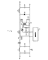
図1は、本実施形態に係る半波型電流共振方式のDC−DCコンバータ1の構成を示す図である。図1に示すDC―DCコンバータ1は、コンデンサC1、C2、C3、C4と、コイルL1、L2、L3と、ダイオードD1、D2と、スイッチング素子Q1と、共振電流モニタ回路10と、制御回路11とを含んで構成されている。
FIG. 1 is a diagram illustrating a configuration of a half-wave current resonance type DC-DC converter 1 according to the present embodiment. A DC-DC converter 1 shown in FIG. 1 includes capacitors C1, C2, C3, and C4, coils L1, L2, and L3, diodes D1 and D2, a switching element Q1, a resonance
以上の構成において、DC−DCコンバータ1に外部から入力される入力直流電圧Vinは、コンデンサC1、C2及びコイルL1によって平滑化されるとともに、ダイオードD1により整流された後、スイッチング素子Q1に入力される。このスイッチング素子Q1は、制御回路11から印加される制御信号によりスイッチング制御される素子であり、所定の周期でオン/オフを繰り返し、入力直流電圧Vinの導通を切り替える。スイッチング素子Q1としては、例えば、MOSFETを用いることができる。なお、制御信号によるスイッチング素子Q1の具体的な制御方法については後述する。
In the above configuration, the input DC voltage Vin input from the outside to the DC-DC converter 1 is smoothed by the capacitors C1, C2 and the coil L1, rectified by the diode D1, and then input to the switching element Q1. The The switching element Q1 is an element that is switching-controlled by a control signal applied from the
制御信号を印加することにより入力直流電圧Vinに対するスイッチング制御が行われると、スイッチング素子Q1からコイルL2及びコンデンサC3を経由して流れる電流は、所定の共振周波数の共振電流Irとなる。コイルL2及びコンデンサC3は、本発明の共振回路として機能し、これらコイルL2及びコンデンサC3の定数により、共振電流Irの共振周波数を調整することができる。 When switching control is performed on the input DC voltage Vin by applying the control signal, the current flowing from the switching element Q1 via the coil L2 and the capacitor C3 becomes a resonance current Ir having a predetermined resonance frequency. The coil L2 and the capacitor C3 function as a resonance circuit of the present invention, and the resonance frequency of the resonance current Ir can be adjusted by the constants of the coil L2 and the capacitor C3.
図1に示すように、スイッチング素子Q1から流れる共振電流Irは、共振電流検出回路としての共振電流モニタ回路10に流れ込む。この共振電流モニタ回路10は、スイッチング素子Q1からの共振電流Irのレベルを常時モニタし、そのレベルに比例した検出信号を制御回路11に出力する。制御回路11では、共振電流モニタ回路10からの検出信号に基づいて共振電流Irがゼロとなるタイミングを判別し、そのタイミングに基づき制御信号の波形パターンを適宜に制御する。
As shown in FIG. 1, the resonance current Ir flowing from the switching element Q1 flows into the resonance
上記の共振電流Irは、ダイオードD2により半波整流され、半波の交流波形となってコイルL3とコンデンサC4に流れ込み、平滑化される。これにより、連続的な波形の直流出力電圧Voutを得ることができ、外部の負荷に接続することにより電力を供給することができる。 The above-described resonance current Ir is half-wave rectified by the diode D2, flows into a half-wave AC waveform, flows into the coil L3 and the capacitor C4, and is smoothed. As a result, a DC output voltage Vout having a continuous waveform can be obtained, and power can be supplied by connecting to an external load.
なお、入力側のコンデンサC1、C2、コイルL1、ダイオードD1、及び出力側のダイオードD2、コイルL3、コンデンサC4は、一体的に本発明の直流化回路として機能する。 The input-side capacitors C1 and C2, the coil L1, the diode D1, and the output-side diode D2, the coil L3, and the capacitor C4 integrally function as a DC circuit of the present invention.
例えば、車載用途のDC−DCコンバータ1を想定すると、Vin=300V程度、Vout=12V程度の入出力電圧に設定して用いることができる。また、共振周波数としては、例えば、500kHz程度に設定することができる。ただし、これらの入出力電圧や共振周波数などは、DC−DCコンバータ1の用途等に応じて適切に設定すること可能である。 For example, assuming a DC-DC converter 1 for in-vehicle use, an input / output voltage of about Vin = 300V and Vout = 12V can be set and used. The resonance frequency can be set to about 500 kHz, for example. However, these input / output voltages, resonance frequencies, and the like can be appropriately set according to the use of the DC-DC converter 1 and the like.
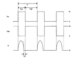
図2は、図1に示すDC−DCコンバータ1における制御信号Vc、スイッチング素子Q1のドレイン・ソース間の電圧Vds、共振電流Irのそれぞれの波形パターンを示す図である。図2に示すように、制御信号Vcはある負荷条件では周期Tでオン/オフを繰り返す矩形波の波形パターンを持ち、Tonの時間だけハイレベルとなってスイッチング素子Q1をオン状態にさせた後、Toffの時間だけローレベルとなってスイッチング素子Q1をオフ状態にさせる。一方、スイッチング素子Q1は、オン状態のときには電圧Vdsがローレベルになって電流が流れるが、オフ状態のときには電圧Vdsがハイレベルとなって電流は流れない。よって、図2に示すように、電圧Vdsは、制御信号Vcの波形と同位相で反転した波形パターンを持つことになる。そして、スイッチング素子Q1がオフからオンに切り替わると同時に後段の共振回路に共振電流Irが流れ始め、コイルL2とコンデンサC3の定数値で定まる波形で変化した後、半波整流されてゼロレベルとなり、それ以降は同様の波形パターンを繰り返す。 FIG. 2 is a diagram showing respective waveform patterns of the control signal Vc, the drain-source voltage Vds of the switching element Q1, and the resonance current Ir in the DC-DC converter 1 shown in FIG. As shown in FIG. 2, the control signal Vc has a rectangular wave waveform pattern that repeats on / off at a period T under a certain load condition, and becomes a high level only for the time Ton to turn on the switching element Q1. , It becomes low level for Toff time, and the switching element Q1 is turned off. On the other hand, when the switching element Q1 is in an on state, the voltage Vds is at a low level and a current flows, but when it is in an off state, the voltage Vds is at a high level and no current flows. Therefore, as shown in FIG. 2, the voltage Vds has a waveform pattern that is inverted in phase with the waveform of the control signal Vc. Then, at the same time when the switching element Q1 is switched from OFF to ON, the resonance current Ir starts to flow through the subsequent resonance circuit, changes in a waveform determined by the constant values of the coil L2 and the capacitor C3, and then half-wave rectified to zero level. Thereafter, the same waveform pattern is repeated.
このとき、図2に示すように、共振電流Irの1周期内では、ゼロとなるタイミングから制御信号Vcがローレベルに切り替わるタイミングまでの遅延時間Tdが存在する。一般に、同様の回路構成に対しては、遅延時間Tdがゼロに近いほど、DC−DCコンバータ1のスイッチング周波数を高くできるため望ましい。しかし、実際には従来の構成を採用した場合、遅延時間Tdは無視できない程度に小さくすることは難しく、特に重負荷状態、つまりスイッチング周波数が高い状態では、周期Tに対して相対的に大きな比率になるため問題となる。 At this time, as shown in FIG. 2, there is a delay time Td from the timing when it becomes zero to the timing when the control signal Vc switches to the low level within one cycle of the resonance current Ir. Generally, for a similar circuit configuration, it is desirable that the delay time Td is closer to zero because the switching frequency of the DC-DC converter 1 can be increased. However, in practice, when the conventional configuration is adopted, it is difficult to reduce the delay time Td to a level that cannot be ignored. It becomes a problem because it becomes.
そこで、本実施形態では、共振電流Irにおける遅延時間Tdを十分に小さく抑え、DC−DCコンバータ1のスイッチング周波数を高くするため、共振電流モニタ回路10を付加することにより共振電流Irがゼロとなるタイミングを判別する構成を採用している。これにより、共振電流モニタ回路10の検出信号を制御回路11にフィードバックしてゼロとなるタイミングを判別し、遅延時間Tdが小さくなるように制御信号の波形パターンを制御することができる。すなわち、後述するようにゼロとなるタイミングを判別したとき、迅速に制御信号Vcをハイレベルからローレベルに切り替え制御することができる。
Therefore, in this embodiment, the resonance current Ir becomes zero by adding the resonance
本実施形態のDC−DCコンバータ1においては、上述の共振電流モニタ回路10として種々の回路構成を適用することができるが、以下では代表的な2種の構成について説明する。第1の実施例では、カレントトランスを用いた共振電流モニタ回路10を構成する場合を示し、第2の実施例では、抵抗及びコンデンサを用いた共振電流モニタ回路を示す。
In the DC-DC converter 1 of the present embodiment, various circuit configurations can be applied as the above-described resonance
図3は、第1の実施例に対応するDC−DCコンバータ1の構成を示す図である。図3に示すように、第1の実施例においては、コンデンサC1、C2、C3、C4、コイルL1、L2、L3、ダイオードD1、D2、スイッチング素子Q1、制御回路11については、図1と同様の構成になっているが、共振電流モニタ回路10は、カレントトランスCTと、抵抗R10、R11、ダイオードD10を含む構成になっている。
FIG. 3 is a diagram showing a configuration of the DC-DC converter 1 corresponding to the first embodiment. As shown in FIG. 3, in the first embodiment, capacitors C1, C2, C3, C4, coils L1, L2, L3, diodes D1, D2, switching element Q1, and
第1の実施例の構成では、スイッチング素子Q1からの共振電流Irは、コイルL2とコンデンサC3との間に挿入されたカレントトランスCTの1次巻線に側に流れ込む。カレントトランスCTは、1次巻線に流れる電流レベルに比例する電圧を2次巻線の側に誘起することができる。すなわち、カレントトランスの2次巻線に生じる電圧レベルを参照することにより、DC−DCコンバータ1の共振電流Irのレベルを検出できることになる。 In the configuration of the first embodiment, the resonance current Ir from the switching element Q1 flows into the primary winding of the current transformer CT inserted between the coil L2 and the capacitor C3. The current transformer CT can induce a voltage proportional to the current level flowing through the primary winding to the secondary winding side. That is, the level of the resonance current Ir of the DC-DC converter 1 can be detected by referring to the voltage level generated in the secondary winding of the current transformer.
図3に示すように、カレントトランスCT10は、2次巻線の一端に終端抵抗としての抵抗R10及び整流用のダイオードD10が接続され、2次巻線の他端が接地されている。そして、カレントトランスCTの2次巻線には、1次巻線の共振電流Irに比例する電圧Vrが発生する。この場合、抵抗R10を調整することにより1次巻線の共振電流Irと2次巻線の電圧Vrの比を決定することができる。なお、抵抗R10を設けない場合は、カレントトランスCTの2次巻線に過大電圧が誘起され、カレントトランスCTの絶縁及び後続の回路を破壊する恐れがある。 As shown in FIG. 3, in the current transformer CT10, a resistor R10 as a termination resistor and a rectifying diode D10 are connected to one end of the secondary winding, and the other end of the secondary winding is grounded. A voltage Vr proportional to the resonance current Ir of the primary winding is generated in the secondary winding of the current transformer CT. In this case, the ratio of the resonance current Ir of the primary winding and the voltage Vr of the secondary winding can be determined by adjusting the resistor R10. If the resistor R10 is not provided, an excessive voltage is induced in the secondary winding of the current transformer CT, and there is a possibility that the insulation of the current transformer CT and the subsequent circuit are destroyed.
また、カレントトランスCTの2次巻線は、整流用のダイオードD10に接続され、このダイオードD10の負荷抵抗として抵抗R11が接続されている。この抵抗R11を調整することにより、ダイオードD10の特性上最適な動作点を設定することができる。そして、制御回路11に対し、カレントトランスCTからダイオードD10を介して共振電流Irに比例する電圧Vrが出力される。
The secondary winding of the current transformer CT is connected to a rectifying diode D10, and a resistor R11 is connected as a load resistance of the diode D10. By adjusting the resistor R11, an optimum operating point can be set in terms of the characteristics of the diode D10. A voltage Vr proportional to the resonance current Ir is output from the current transformer CT to the
制御回路11は、共振電流Irが所定の周期で流れている際、入力された電圧Vrのレベルを監視する。そして、電圧Vrが大きいレベルが徐々に減少してゼロとなるタイミングを判別し、その時点でハイレベルとなっている制御信号をローレベルに切り替えるように制御する。これにより、図2における遅延時間Tdを最小限に抑え、スイッチング周波数を高くすることができる。
The
また、制御回路11は、過大な共振電流Irが流れることを防止するため、電圧Vrが所定値を超えたときに、制御信号をローレベルに切り替えるように制御してもよい。このように制御することにより、スイッチング素子Q1に定められている定格を超えるような電流が流れることを防止でき、異常動作や破壊を確実に防止して信頼性を向上させることができる。
Further, the
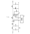
次に図4は、第2の実施例に対応するDC−DCコンバータ1の構成を示す図である。図4に示すように、第2の実施例においても、コンデンサC1、C2、C3、C4、コイルL1、L2、L3、ダイオードD1、D2、スイッチング素子Q1、制御回路11については、図1と同様の構成になっている。一方、共振電流モニタ回路10の構成は、第1の実施例と異なり、直列接続されたコンデンサC20及び抵抗R20からなる分流回路を含んで構成されている。
Next, FIG. 4 is a diagram showing a configuration of the DC-DC converter 1 corresponding to the second embodiment. As shown in FIG. 4, in the second embodiment, capacitors C1, C2, C3, C4, coils L1, L2, L3, diodes D1, D2, switching element Q1, and
第2の実施例の構成では、スイッチング素子Q1からコイルL2を介して流れる共振電流Irは、大部分はコンデンサC3の側に流れるが、一部がコンデンサC20及び抵抗R20の側に分流する。これらのコンデンサC20及び抵抗R20は分流回路を構成し、共振電流Irのレベルの検出に用いられる(以下、検出コンデンサC20、検出抵抗R20と呼ぶ)。 In the configuration of the second embodiment, most of the resonance current Ir flowing from the switching element Q1 via the coil L2 flows to the capacitor C3 side, but part of the resonance current Ir is shunted to the capacitor C20 and the resistor R20 side. The capacitor C20 and the resistor R20 constitute a shunt circuit and are used for detecting the level of the resonance current Ir (hereinafter referred to as a detection capacitor C20 and a detection resistor R20).
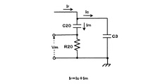
ここで、図5は、図4に示すDC−DCコンバータ1の構成のうち、コンデンサC20、抵抗R20、コンデンサC3の部分の拡大図である。図5に示すように、共振電流Irに対し、コンデンサC3の側に流れる電流をIc、検出コンデンサC20及び検出抵抗R20の側に流れる電流をImとすると、次の(1)式が成り立つ。 Here, FIG. 5 is an enlarged view of a portion of the capacitor C20, the resistor R20, and the capacitor C3 in the configuration of the DC-DC converter 1 shown in FIG. As shown in FIG. 5, with respect to the resonance current Ir, if the current flowing on the capacitor C3 side is Ic and the current flowing on the detection capacitor C20 and detection resistor R20 side is Im, the following equation (1) is established.
Ir=Ic+Im (1)
検出抵抗R20を十分小さい値とした場合には、検出コンデンサC20及び検出抵抗R20の合成インピーダンスにおける抵抗R20の寄与分を無視することができる。この場合、電流Icと電流Im(以下、検出電流Imと呼ぶ)との関係は、次の(2)式で表すことができる。
Ir = Ic + Im (1)
When the detection resistor R20 is set to a sufficiently small value, the contribution of the resistor R20 in the combined impedance of the detection capacitor C20 and the detection resistor R20 can be ignored. In this case, the relationship between the current Ic and the current Im (hereinafter referred to as the detection current Im) can be expressed by the following equation (2).
Ic=Im×C3/C20 (2)
このように、電流Icと検出電流Imは、比例関係にあり、同様の波形を有することがわかる。ここで、検出抵抗R20の両端の電圧をVmとすると、検出電流Imは、次の(3)式で表される。
Ic = Im × C3 / C20 (2)
Thus, it can be seen that the current Ic and the detection current Im are in a proportional relationship and have a similar waveform. Here, if the voltage across the detection resistor R20 is Vm, the detection current Im is expressed by the following equation (3).
Im=Vm/R20 (3)
制御回路20においては電圧Vmが取得されるので、(3)式に従って検出電流Imを求めることができる。このように求めた検出電流Imに基づき、(2)式に従って電流Icを算出すると、電流Icに概ね一致する共振電流Irを推測できることになる。
Im = Vm / R20 (3)
Since the voltage Vm is acquired in the control circuit 20, the detection current Im can be obtained according to the equation (3). If the current Ic is calculated according to the equation (2) based on the detected current Im thus obtained, the resonance current Ir that roughly matches the current Ic can be estimated.
分流回路を構成するコンデンサC20と抵抗R20の定数は、適正な範囲に選定する必要がある。まず、コンデンサC20については、容量を大きくし過ぎると、検出電流Imが大きくなって、電流Icに対して無視できなくなるので、少なくともコンデンサC3の1/100程度以下に選定することが望ましい。また、抵抗R20については、両端の電圧Vmがある程度確保できる程度に選定することが望ましく、5〜10V程度の電圧Vmが発生すれば十分である。なお、電圧Vmが小さい場合は、例えば、オペアンプ等を用いて所定のゲインで増幅する構成を採用してもよい。 The constants of the capacitor C20 and the resistor R20 constituting the shunt circuit must be selected within an appropriate range. First, regarding the capacitor C20, if the capacitance is increased too much, the detection current Im becomes large and cannot be ignored with respect to the current Ic. Therefore, it is desirable to select at least about 1/100 or less of the capacitor C3. The resistor R20 is preferably selected so that the voltage Vm at both ends can be secured to some extent, and it is sufficient that a voltage Vm of about 5 to 10 V is generated. When the voltage Vm is small, for example, a configuration in which amplification is performed with a predetermined gain using an operational amplifier or the like may be employed.
ここで、具体例として、図5の構成における各定数を次のように定める場合を考える。 Here, as a specific example, consider a case where each constant in the configuration of FIG. 5 is determined as follows.
C3 =0.198μF
C20=330pF
R20=100Ω
この条件の下、制御回路11にて電圧Vmのピーク値6Vが検出された場合を考える。このとき、検出コンデンサC20及び検出抵抗R21を流れる電流Imのピーク値は、(3)式に従って、
Im=6/100=0.06(A0-p)
と算出することができる。その算出結果と(2)式に基づき、コンデンサC3を流れる電流Icのピーク値は、
Ic=Im×0.198μF/330pF=0.06×600=36(A0-p)
と推定することができる。一方、(1)式において、検出電流Imが無視できる程度に小さいので、共振電流Irのピーク値もほぼ36(A0-p)になるものと推定することができる。
C3 = 0.198 μF
C20 = 330pF
R20 = 100Ω
Consider the case where the
Im = 6/100 = 0.06 (A 0-p )
Can be calculated. Based on the calculation result and equation (2), the peak value of the current Ic flowing through the capacitor C3 is
Ic = Im × 0.198 μF / 330 pF = 0.06 × 600 = 36 (A 0-p )
Can be estimated. On the other hand, in the equation (1), since the detection current Im is small enough to be ignored, it can be estimated that the peak value of the resonance current Ir is approximately 36 (A 0-p ).
そして、共振電流Irのゼロとなるタイミングを判別する場合は、(1)〜(3)式に基づいて、Vm=0のときにIr=0となる関係にあるので、制御回路11で常に電圧Vmを監視することにより、ゼロとなるタイミングを検出することができる。制御回路11では、第1の実施例の場合と同様、ゼロとなるタイミングを判別した時点でハイレベルとなっている制御信号を直ちにローレベルに切り替えるように制御すればよい。
When determining when the resonance current Ir becomes zero, based on the equations (1) to (3), Ir = 0 when Vm = 0. By monitoring Vm, it is possible to detect the timing when it becomes zero. As in the first embodiment, the
なお、過大な共振電流Irが流れることを防止する際も、上述の算出方法に従って共振電流Irを求めた上で、第1の実施例と同様の制御を行うことができる。 In order to prevent the excessive resonance current Ir from flowing, the same control as in the first embodiment can be performed after the resonance current Ir is obtained according to the above-described calculation method.
このように、第2の実施例によれば、一般的なコンデンサと抵抗を用いて共振電流モニタ回路10を構成することができ、大型の部品は不要であるので、DC−DCコンバータ1の構成の小型化及び低コスト化の面で有利である。また、コンデンサと抵抗を配置するための回路パターンを短くすることができる。これにより、浮遊インダクタンスを抑えてDC−DCコンバータ1の共振周波数を高くすることができるとともに、小型化にも一層好適である。
As described above, according to the second embodiment, the resonance
なお、上記の実施形態では、本発明を半波型電流共振方式のDC−DCコンバータに対して適用する場合を説明したが、これに限られることなく、入力電圧の導通をスイッチング素子によって制御し、共振電流を発生させて、それにより直流出力電圧を出力して負荷に供給する構成を備えたスイッチング電源回路に対し、広く本発明を適用することが可能である。 In the above embodiment, the case where the present invention is applied to a half-wave current resonance type DC-DC converter has been described. However, the present invention is not limited to this, and the conduction of the input voltage is controlled by the switching element. The present invention can be widely applied to a switching power supply circuit having a configuration in which a resonance current is generated and thereby a DC output voltage is output and supplied to a load.
1…DC−DCコンバータ
10…共振電流モニタ回路
11…制御回路
C1、C2、C3、C4、C20…コンデンサ
L1、L2、L3…コイル
D1、D2、D10…ダイオード
R10、R11、R20…抵抗
Vin…入力直流電圧
Vout…直流出力電圧
Ir…共振電流
DESCRIPTION OF SYMBOLS 1 ... DC-
Claims (10)
制御信号に基づき前記入力電圧の導通を切り替え可能に制御するスイッチング素子と、
前記スイッチング素子の出力側に接続され、所定の共振周波数の共振電流を発生させる共振回路と、
前記共振電流に応じて発生する出力電圧を半波整流して平滑化し、前記直流出力電圧を出力する直流化回路と、
前記共振電流のレベルを検出する共振電流検出回路と、
前記共振電流検出回路により検出された前記共振電流のレベルに基づき前記制御信号の波形を制御して前記スイッチング素子に供給する制御回路と、
を備えることを特徴とするスイッチング電源回路。 A switching power supply circuit that performs switching control of an input voltage at a predetermined frequency to generate a DC output voltage and supplies the DC output voltage to a load,
A switching element that controls switching of the conduction of the input voltage based on a control signal;
A resonance circuit connected to the output side of the switching element and generating a resonance current of a predetermined resonance frequency;
A DC circuit that outputs the DC output voltage by smoothing the output voltage generated according to the resonance current by half-wave rectification;
A resonance current detection circuit for detecting a level of the resonance current;
A control circuit for controlling the waveform of the control signal based on the level of the resonance current detected by the resonance current detection circuit and supplying the control signal to the switching element;
A switching power supply circuit comprising:
制御信号に基づき前記入力直流電圧の導通を切り替え可能に制御するスイッチング素子と、
前記スイッチング素子の出力側に接続され、所定の共振周波数の共振電流を発生させる共振回路と、
前記共振電流に応じて発生する出力電圧を半波整流して平滑化し、前記直流出力電圧を出力する直流化回路と、
前記共振電流のレベルを検出する共振電流検出回路と、
前記共振電流検出回路により検出された前記共振電流のレベルに基づき前記制御信号の波形を制御して前記スイッチング素子に供給する制御回路と、
を備えることを特徴とするDC−DCコンバータ。 A DC-DC converter that generates a DC output voltage by switching the input DC voltage at a predetermined frequency and supplies the DC output voltage to a load.
A switching element that controls switching of conduction of the input DC voltage based on a control signal;
A resonance circuit connected to the output side of the switching element and generating a resonance current of a predetermined resonance frequency;
A DC circuit that outputs the DC output voltage by smoothing the output voltage generated according to the resonance current by half-wave rectification;
A resonance current detection circuit for detecting a level of the resonance current;
A control circuit for controlling the waveform of the control signal based on the level of the resonance current detected by the resonance current detection circuit and supplying the control signal to the switching element;
A DC-DC converter comprising:
10. The DC-DC converter according to claim 9, wherein the control circuit switches and controls the control signal so that the switching element is turned off at a timing when the resonance current becomes zero.
Priority Applications (1)
| Application Number | Priority Date | Filing Date | Title |
|---|---|---|---|
| JP2004104564A JP2005295636A (en) | 2004-03-31 | 2004-03-31 | Switching power supply circuit and DC-DC converter |
Applications Claiming Priority (1)
| Application Number | Priority Date | Filing Date | Title |
|---|---|---|---|
| JP2004104564A JP2005295636A (en) | 2004-03-31 | 2004-03-31 | Switching power supply circuit and DC-DC converter |
Publications (1)
| Publication Number | Publication Date |
|---|---|
| JP2005295636A true JP2005295636A (en) | 2005-10-20 |
Family
ID=35327974
Family Applications (1)
| Application Number | Title | Priority Date | Filing Date |
|---|---|---|---|
| JP2004104564A Pending JP2005295636A (en) | 2004-03-31 | 2004-03-31 | Switching power supply circuit and DC-DC converter |
Country Status (1)
| Country | Link |
|---|---|
| JP (1) | JP2005295636A (en) |
Citations (6)
| Publication number | Priority date | Publication date | Assignee | Title |
|---|---|---|---|---|
| JPH02211054A (en) * | 1989-02-07 | 1990-08-22 | Nec Corp | Current resonance converter |
| JPH02311168A (en) * | 1989-05-26 | 1990-12-26 | Nec Corp | Pulse width control current resonance converter |
| JPH0378465A (en) * | 1989-08-17 | 1991-04-03 | Oki Electric Ind Co Ltd | Control circuit for current resonance type power supply |
| JPH09331673A (en) * | 1996-06-10 | 1997-12-22 | Matsushita Electric Ind Co Ltd | Current resonance type DC-DC converter |
| JP2001292571A (en) * | 2000-04-07 | 2001-10-19 | Yokogawa Electric Corp | Synchronous rectification circuit |
| JP2002058240A (en) * | 2000-06-01 | 2002-02-22 | Auto Network Gijutsu Kenkyusho:Kk | DC-DC converter circuit |
-
2004
- 2004-03-31 JP JP2004104564A patent/JP2005295636A/en active Pending
Patent Citations (6)
| Publication number | Priority date | Publication date | Assignee | Title |
|---|---|---|---|---|
| JPH02211054A (en) * | 1989-02-07 | 1990-08-22 | Nec Corp | Current resonance converter |
| JPH02311168A (en) * | 1989-05-26 | 1990-12-26 | Nec Corp | Pulse width control current resonance converter |
| JPH0378465A (en) * | 1989-08-17 | 1991-04-03 | Oki Electric Ind Co Ltd | Control circuit for current resonance type power supply |
| JPH09331673A (en) * | 1996-06-10 | 1997-12-22 | Matsushita Electric Ind Co Ltd | Current resonance type DC-DC converter |
| JP2001292571A (en) * | 2000-04-07 | 2001-10-19 | Yokogawa Electric Corp | Synchronous rectification circuit |
| JP2002058240A (en) * | 2000-06-01 | 2002-02-22 | Auto Network Gijutsu Kenkyusho:Kk | DC-DC converter circuit |
Similar Documents
| Publication | Publication Date | Title |
|---|---|---|
| JP6528561B2 (en) | High efficiency power factor correction circuit and switching power supply | |
| KR100428329B1 (en) | Switched mode power supply with power factor correction | |
| US7936152B2 (en) | Switching power source | |
| US8077488B2 (en) | Switching-type power-supply unit and a method of switching in power-supply unit | |
| JP2008535456A (en) | Control of resonant converter | |
| US10355610B2 (en) | LLC power converter and switching method thereof | |
| JP4104609B2 (en) | Method for controlling the current and voltage of a switch mode power supply unit | |
| JP4854556B2 (en) | Power supply | |
| US7719139B2 (en) | Power supply unit | |
| JPH07241075A (en) | Current detection device and method in power conversion | |
| US6985369B2 (en) | DC-DC converter | |
| JP4352460B2 (en) | Power supply | |
| JP5194665B2 (en) | Power supply | |
| US6580624B2 (en) | Switching power circuit with a filter for controlling noise of a switching frequency and method of same | |
| CN100583615C (en) | Resonant converter and its control device and control method | |
| JP2005295636A (en) | Switching power supply circuit and DC-DC converter | |
| JP2010081779A (en) | Power-supply apparatus and switching method therefor | |
| JPH09168281A (en) | Dc power source apparatus | |
| JP2002125367A (en) | Power supply | |
| JP2003259642A (en) | Contactless power supply | |
| JP3001057B1 (en) | Switching power supply device and control method thereof | |
| JP3571959B2 (en) | Switching power supply | |
| JP3056179B2 (en) | Instantaneous interruption prevention circuit | |
| JP2002142456A (en) | Dc power supply apparatus | |
| JPH05336747A (en) | Switching power supply |
Legal Events
| Date | Code | Title | Description |
|---|---|---|---|
| A621 | Written request for application examination |
Free format text: JAPANESE INTERMEDIATE CODE: A621 Effective date: 20070201 |
|
| RD03 | Notification of appointment of power of attorney |
Free format text: JAPANESE INTERMEDIATE CODE: A7423 Effective date: 20081022 |
|
| A977 | Report on retrieval |
Effective date: 20091007 Free format text: JAPANESE INTERMEDIATE CODE: A971007 |
|
| A131 | Notification of reasons for refusal |
Free format text: JAPANESE INTERMEDIATE CODE: A131 Effective date: 20091020 |
|
| A521 | Written amendment |
Effective date: 20091218 Free format text: JAPANESE INTERMEDIATE CODE: A523 |
|
| A131 | Notification of reasons for refusal |
Free format text: JAPANESE INTERMEDIATE CODE: A131 Effective date: 20100202 |
|
| A02 | Decision of refusal |
Effective date: 20100601 Free format text: JAPANESE INTERMEDIATE CODE: A02 |
|
| RD02 | Notification of acceptance of power of attorney |
Effective date: 20100818 Free format text: JAPANESE INTERMEDIATE CODE: A7422 |
|
| RD04 | Notification of resignation of power of attorney |
Free format text: JAPANESE INTERMEDIATE CODE: A7424 Effective date: 20100818 |