JP2005295364A - Manufacturing method of surface acoustic wave device - Google Patents
Manufacturing method of surface acoustic wave device Download PDFInfo
- Publication number
- JP2005295364A JP2005295364A JP2004109783A JP2004109783A JP2005295364A JP 2005295364 A JP2005295364 A JP 2005295364A JP 2004109783 A JP2004109783 A JP 2004109783A JP 2004109783 A JP2004109783 A JP 2004109783A JP 2005295364 A JP2005295364 A JP 2005295364A
- Authority
- JP
- Japan
- Prior art keywords
- acoustic wave
- wafer
- surface acoustic
- thin film
- piezoelectric thin
- Prior art date
- Legal status (The legal status is an assumption and is not a legal conclusion. Google has not performed a legal analysis and makes no representation as to the accuracy of the status listed.)
- Pending
Links
Images
Landscapes
- Surface Acoustic Wave Elements And Circuit Networks Thereof (AREA)
Abstract
Description
本発明は、主に移動体通信機器などで使用される弾性表面波素子の製造方法に関するものである。 The present invention relates to a method for manufacturing a surface acoustic wave element mainly used in mobile communication devices and the like.
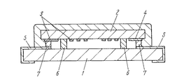
以下、従来の弾性表面波素子の製造方法を図3により説明する。図3は、従来の弾性表面波素子の断面図である。 Hereinafter, a conventional method of manufacturing a surface acoustic wave device will be described with reference to FIG. FIG. 3 is a cross-sectional view of a conventional surface acoustic wave element.
図3に示すごとく、基板1は、その上面に弾性表面波チップ2を有する。この弾性表面波チップ2は、一方の面に櫛形電極3を有し、この櫛形電極3を有する面が基板1側になるように載置したものである。櫛形電極3は、入出力電極4を介して外部取出電極5と電気的に接続されている。外部取出電極5は、基板1の弾性表面波チップ2側から、その反対側に電極を取出すように形成した。
As shown in FIG. 3, the
このような弾性表面波素子は、次のように製造される。 Such a surface acoustic wave element is manufactured as follows.
すなわち、まず、櫛形電極3を形成した圧電体ウエハ(図示せず)を切断して個別の弾性表面波チップ2を形成する。次に、半導体ウエハ(図示せず)上に、環状部材6を介して櫛形電極3が下面に向くように弾性表面波チップ2を、一つ一つ位置合わせ(アライメント)しながら実装する。その後、接合部材7により、入出力電極4を外部取出電極5に接続する。
That is, first, a piezoelectric wafer (not shown) on which the comb electrodes 3 are formed is cut to form individual surface
次に、離型性に優れた、例えば、フッ素樹脂からなる枠(図示せず)を基板1上に載置して各弾性表面波チップ2を囲み、封止用の樹脂(図示せず)を流し込むことにより樹脂ポッティングを行い、加熱して樹脂を硬化させる。
Next, a frame (not shown) made of, for example, a fluororesin having excellent releasability is placed on the
最後に、枠を外した後、半導体ウエハをダイシングすることにより、個々の弾性表面波素子を切り出す。 Finally, after removing the frame, each surface acoustic wave element is cut out by dicing the semiconductor wafer.
なお、本発明に関連する先行技術文献としては、例えば、特許文献1が知られている。
しかしながら、上記従来の構成では、弾性表面波素子の生産性が低いという課題があった。すなわち、従来は基板1上に、環状部材6を介して櫛形電極3が下面に向くように弾性表面波チップ2を載置する。このような弾性表面波素子を製造するにはまず圧電体ウエハを切断して個別の弾性表面波チップ2を形成し、次にこの弾性表面波チップ2を半導体ウエハ上に一つ一つ、接続位置のアライメントを行いながら実装し、さらに封止後にこの半導体ウエハを切断して、個々の弾性表面波素子を得ていた。このため、弾性表面波チップ2を基板1に一つ一つアライメントしながら実装する前後で、圧電体ウエハの切断および半導体ウエハの切断をするという2回の切断工程を有するので生産性が低くなるという課題があった。
However, the conventional configuration has a problem that the productivity of the surface acoustic wave element is low. That is, conventionally, the surface
そこで、本発明は、弾性表面波素子の生産性を高めることを目的とするものである。 Accordingly, the present invention aims to increase the productivity of surface acoustic wave elements.
そして、この目的を達成するために、本発明は、特に、ウエハに複数のスルーホールを形成し、次にこのスルーホールに導電性材料を充填し、その後このスルーホールを形成したウエハの表面に圧電体薄膜を設け、次にこの圧電体薄膜の上面に少なくとも複数の櫛形電極を設け、その後前記圧電体薄膜の表面の前記櫛形電極をその外部分で封止し、次にこの封止後のウエハを切断して個片とすることを特徴とする。 In order to achieve this object, the present invention particularly forms a plurality of through holes in the wafer, then fills the through holes with a conductive material, and then forms the through holes on the surface of the wafer. A piezoelectric thin film is provided, and then at least a plurality of comb-shaped electrodes are provided on the upper surface of the piezoelectric thin film, and then the comb-shaped electrodes on the surface of the piezoelectric thin film are sealed at an outer portion thereof. The wafer is cut into individual pieces.
本発明の効果は、弾性表面波素子の生産性を高めることである。すなわち、スルーホールが形成された基板上に圧電体薄膜を形成するため、基板は一枚でよく、弾性表面波素子を得るための切断工程は、封止後にこの基板を切断する一度の切断工程のみでよい。この結果として、弾性表面波素子の生産性を高めることができる。 The effect of the present invention is to increase the productivity of the surface acoustic wave device. That is, since the piezoelectric thin film is formed on the substrate in which the through holes are formed, the number of the substrates may be one, and the cutting process for obtaining the surface acoustic wave element is a single cutting process for cutting the substrate after sealing. Only need. As a result, the productivity of the surface acoustic wave element can be increased.
(実施の形態1)
以下、本発明の実施の形態について、図面を用いて説明する。
(Embodiment 1)
Hereinafter, embodiments of the present invention will be described with reference to the drawings.
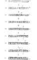
図1は、本実施の形態1の弾性表面波素子の製造方法を示した工程フロー図である。図1(A)〜図2(P)までの各図はそれぞれの工程での半導体ウエハの断面図を示している。工程の順を追って本発明の製造方法を説明する。 FIG. 1 is a process flow diagram illustrating a method for manufacturing a surface acoustic wave device according to the first embodiment. Each of FIGS. 1A to 2P is a cross-sectional view of a semiconductor wafer in each process. The manufacturing method of the present invention will be described in the order of the steps.
図1(A)は、加工前のウエハ、すなわち、シリコン基板8のウエハの状態を示している。
FIG. 1A shows the state of the wafer before processing, that is, the wafer of the
まず、このようなシリコン基板8のウエハの所望の位置に、図1(B)に示すように、シリコンエッチング工程として、直径10μm〜100μm程度貫通してスルーホール9を厚み方向に形成する。
First, as shown in FIG. 1B, a through hole 9 is formed in the thickness direction through a diameter of about 10 μm to 100 μm at a desired position on the wafer of the
次に、図1(C)に示すように、壁面絶縁工程として、スルーホール9の内壁およびシリコン基板8の表面に絶縁膜10を形成する。その後、絶縁膜10を形成したスルーホール9に、金属充填工程として、図1(D)に示すように、導電性材料11を充填する。これらシリコンエッチング工程、壁面絶縁工程、金属充填工程という一連の工程を、以下、スルーホール形成工程と呼ぶ。ここまでの工程を経た基板を以下スルーホール形成ウエハ12と呼ぶ。
Next, as shown in FIG. 1C, an
その後、図1(E)に示すように、圧電体薄膜形成工程として、スルーホール形成ウエハ12の上面に圧電体薄膜13を形成する。この圧電体薄膜13を形成したウエハは圧電体薄膜ウエハ14と以下では呼び、これ以降の工程のウエハについて、圧電体薄膜の形成された面を表面、反対側の面を裏面とする。
Thereafter, as shown in FIG. 1E, a piezoelectric
次に、図1(F)に示すように、圧電体薄膜除去工程として、圧電体薄膜13のうちスルーホール9の上面にあたる部分をエッチング等によって除去する。このエッチング処理により、圧電体薄膜のスルーホール9の上面にあたる部分に開口部15を設け、表面にスルーホール内部の導電性材料11を露出する。
Next, as shown in FIG. 1F, as a piezoelectric thin film removing step, a portion corresponding to the upper surface of the through hole 9 in the piezoelectric
その後、図1(G)に示すように、電極膜形成工程として、圧電体薄膜除去工程を経た圧電体薄膜ウエハ14の表面全面に蒸着やスパッタリングなどの方法によって電極膜16を形成する。
Thereafter, as shown in FIG. 1G, as the electrode film forming step, the electrode film 16 is formed on the entire surface of the piezoelectric
次に、図1(H)に示すように、電極パターン形成工程として、圧電体薄膜ウエハ14の表面に形成した電極膜16を、フォトリソグラフィによってパターンニングし、電極パッド17と櫛形電極18とを形成する。この電極パッド17は、開口部15の上面に設けたものであり、スルーホール9内に充填した導電性材料11と接続している。また、電極パッド17と櫛形電極18とは配線用電極(図示せず)で接続されている。このため、櫛形電極18は、電極パッド17を介して導電性材料11と電気的に接続されている。これにより、圧電体薄膜ウエハ14の裏面側に、後述する図1(I)のように再配線用電極膜19を設けると、櫛形電極18に、圧電体薄膜ウエハ14の裏面側から給電することが可能になる。
Next, as shown in FIG. 1H, as an electrode pattern forming step, the electrode film 16 formed on the surface of the piezoelectric
この圧電体薄膜除去工程、電極膜形成工程、電極パターン形成工程はあわせて、以下、電極形成工程と呼ぶ。 The piezoelectric thin film removing process, the electrode film forming process, and the electrode pattern forming process are collectively referred to as an electrode forming process.
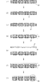
その後、図1(I)に示すように、再配線用電極膜形成工程として、電極形成工程を経た圧電体薄膜ウエハ14の裏面側の全面に再配線用電極膜19を形成する。次に、図2(J)に示すように、再配線用電極パターン形成工程として、フォトリソグラフィ等によって再配線用電極膜20を形成する。
Thereafter, as shown in FIG. 1I, a rewiring
その後、図2(K)に示すように、再配線用電極膜形成工程、再配線用電極パターン形成工程を経た圧電体薄膜ウエハ14の裏面側にさらに絶縁膜21を作製する。次に、図2(L)に示すように、この絶縁膜21をフォトリソグラフィによって、外部端子用開口部22を作製する。その後、図2(M)に示すように、外部端子形成工程として、外部端子用開口部22に外部端子23をスパッタリングあるいは、メッキ法、あるいはその組み合わせによって形成する。この外部端子23は、弾性表面波素子が外部の回路と接続することを可能にする。
Thereafter, as shown in FIG. 2K, an insulating film 21 is further formed on the back surface side of the piezoelectric
ここまでのプロセスを経たウエハを以下、弾性表面波素子ウエハ24と呼ぶ。 The wafer that has undergone the processes so far is hereinafter referred to as a surface acoustic wave element wafer 24.
次に、弾性表面波素子ウエハ24を接着するため、図2(N)に示すような樹脂フィルム25を用意する。この樹脂フィルム25は、弾性表面波素子ウエハ24側の面に、櫛形電極18に対応する部分が開口するように、あらかじめ接着剤26が塗布されている。この樹脂フィルム25は、図2(O)に示すように、弾性表面波素子ウエハ24の表面に接着され、櫛形電極18などの各電極をウエハ状態のままで封止する。
Next, in order to bond the surface acoustic wave element wafer 24, a
この工程を経たウエハを以下では封止後ウエハ27と呼ぶ。 The wafer that has undergone this process is hereinafter referred to as a post-sealing wafer 27.
最後に、図2(P)に示すように、この封止後ウエハ27を所望の個片が得られるように切断して、弾性表面波素子28が完成する。
Finally, as shown in FIG. 2 (P), the wafer 27 after sealing is cut so as to obtain a desired piece, whereby the surface
以上に示したような弾性表面波素子28の製造方法によれば、弾性表面波素子28の生産性を高めることができる。すなわち、スルーホール9が作製されたシリコン基板8上に圧電体薄膜13を形成するため弾性表面波素子28を得るための切断工程は、封止後にこの半導体基板を図2(P)のごとく切断する一度の切断工程のみでよい。この結果として、弾性表面波素子28の生産性を高めることができる。
According to the method for manufacturing the surface
また、シリコン基板8を使うので、従来の弾性表面波素子の作製プロセスでは考えられない大判のウエハで低コストでの製造が可能になる。
Further, since the
なお、図1(B)に示したシリコンエッチング工程は、直径数十ミクロンの穴を300μmから600μmの厚みのシリコンウエハに垂直に貫通加工する必要があるが、ドライエッチングで行えば可能である。これにより、スルーホール9の壁面の垂直性を高めることができ、スルーホール9の占める領域をより小さくできるという作用を有する。 In the silicon etching step shown in FIG. 1B, a hole having a diameter of several tens of microns needs to be vertically penetrated into a silicon wafer having a thickness of 300 μm to 600 μm, but can be performed by dry etching. Thereby, the perpendicularity of the wall surface of the through hole 9 can be improved, and the area occupied by the through hole 9 can be further reduced.
また、図1(C)に示した壁面絶縁工程は、シリコン基板8を熱酸化させて行うと好ましい。この場合、スルーホール9の内部の側壁だけなく、シリコン基板8の両面にも酸化膜ができるが、圧電体薄膜13の密着性や、さらにこの後に形成される電極パッド17、櫛形電極18、再配線用電極膜19,20とシリコン基板8の間を絶縁することができ、むしろ好都合である。さらに、このシリコン基板8の両面に形成された酸化膜は、シリコン基板8の表面が荒れることを防ぎ、圧電体薄膜13の結晶性への影響も少ない。なお、壁面に絶縁膜21を形成する工法としては、他にCVD法があるが、膜厚のコントロールや面の平坦度、装置コストなどから不利である。ただし、熱酸化法はプロセス温度が高いので、この一連の弾性表面波素子の作製プロセスの最初に行う必要がある。
Moreover, it is preferable that the wall surface insulating step shown in FIG. 1C is performed by thermally oxidizing the
さらに、図1(D)に示すように、金属充填工程におけるスルーホール9への導電性材料11の充填は、メッキ法の他にペースト状の金属を埋めて焼成することで実現できるが、プロセスの選択によってはシリコン基板8の両面より外側にはみ出すこともある。その場合は、両面研磨によって平坦化する必要がある。両面研磨を行うと、図1(C)に示した壁面絶縁工程で作製したシリコン基板8の両面の熱酸化膜10が除去されてしまう。また、最初の基板厚みよりも厚みの薄い弾性表面波素子28を作製するときも、再配線用電極膜形成工程の手前までのいずれかの工程の間に少なくとも裏面側を研磨する必要がある。
Furthermore, as shown in FIG. 1D, the filling of the
この場合は研磨後に酸化膜の形成工程を入れるとよい。この酸化膜の形成は蒸着、スパッタリング法などのいずれかの方法で行う。また、絶縁膜21としては、樹脂でもよくポリイミドであれば、耐熱性もあり膜厚のコントロールも容易であるので好ましい。 In this case, an oxide film forming step may be added after polishing. The oxide film is formed by any method such as vapor deposition or sputtering. As the insulating film 21, a resin or polyimide is preferable because it has heat resistance and the film thickness can be easily controlled.
なお、圧電体薄膜除去工程においては、開口部15の外形はスルーホール9の外形より内側にすることが好ましい。すなわち、電極パッド17の外形は開口部15の外形よりも大きくなるが、このようにすれば、電極パッド17のサイズを抑えることができる。
In the piezoelectric thin film removing step, it is preferable that the outer shape of the
また、封止後ウエハ27をダイシング加工する際、ダイシングテープ(図示せず)などの機材に封止後ウエハ27を固定して切断する。このときに封止後ウエハ27の裏面を固定して切断するとよい。図示していないが、弾性表面波素子28はパッケージ外周部を金属でシールドする場合がある。封止後ウエハ27の裏面を固定し、ハーフダイシングで溝を入れた後、メッキ等で金属膜を形成すれば、ウエハ状態のままでシールドを形成することができるのである。
In addition, when dicing the post-sealing wafer 27, the post-sealing wafer 27 is fixed to a device such as a dicing tape (not shown) and cut. At this time, the back surface of the wafer 27 after sealing may be fixed and cut. Although not shown, the surface
本発明は、弾性表面波素子の生産性を高めることができるという効果を有し、主に移動体通信機器などで使用される弾性表面波素子に有用である。すなわち、スルーホールを形成した導体基板上に圧電体薄膜を形成するため、弾性表面波素子を得るための切断工程は、封止後にこの半導体基板を切断する一度の切断工程のみでよい。この結果として、弾性表面波素子の生産性を高めることができ、主に移動体通信機器などで使用される弾性表面波素子に有用である。 INDUSTRIAL APPLICABILITY The present invention has an effect that the productivity of a surface acoustic wave element can be increased, and is useful for a surface acoustic wave element mainly used in mobile communication equipment and the like. That is, since the piezoelectric thin film is formed on the conductor substrate in which the through hole is formed, the cutting process for obtaining the surface acoustic wave element may be only a single cutting process for cutting the semiconductor substrate after sealing. As a result, the productivity of the surface acoustic wave element can be increased, which is useful for a surface acoustic wave element mainly used in mobile communication devices.
8 シリコン基板
9 スルーホール
10 絶縁膜(熱酸化膜)
11 導電性材料
12 スルーホール形成ウエハ
13 圧電体薄膜
14 圧電体薄膜ウエハ
15 開口部
16 電極膜
17 電極パッド
18 櫛形電極
19,20 再配線用電極膜
21 絶縁膜
22 外部端子用開口部
23 外部端子
24 弾性表面波素子ウエハ
25 樹脂フィルム
26 接着剤
27 封止後ウエハ
28 弾性表面波素子
8 Silicon substrate 9 Through
DESCRIPTION OF
Claims (5)
Priority Applications (1)
| Application Number | Priority Date | Filing Date | Title |
|---|---|---|---|
| JP2004109783A JP2005295364A (en) | 2004-04-02 | 2004-04-02 | Manufacturing method of surface acoustic wave device |
Applications Claiming Priority (1)
| Application Number | Priority Date | Filing Date | Title |
|---|---|---|---|
| JP2004109783A JP2005295364A (en) | 2004-04-02 | 2004-04-02 | Manufacturing method of surface acoustic wave device |
Publications (1)
| Publication Number | Publication Date |
|---|---|
| JP2005295364A true JP2005295364A (en) | 2005-10-20 |
Family
ID=35327782
Family Applications (1)
| Application Number | Title | Priority Date | Filing Date |
|---|---|---|---|
| JP2004109783A Pending JP2005295364A (en) | 2004-04-02 | 2004-04-02 | Manufacturing method of surface acoustic wave device |
Country Status (1)
| Country | Link |
|---|---|
| JP (1) | JP2005295364A (en) |
Cited By (1)
| Publication number | Priority date | Publication date | Assignee | Title |
|---|---|---|---|---|
| US8275158B2 (en) | 2009-10-12 | 2012-09-25 | Samsung Electronics Co., Ltd. | Piezoelectric micro speaker |
-
2004
- 2004-04-02 JP JP2004109783A patent/JP2005295364A/en active Pending
Cited By (1)
| Publication number | Priority date | Publication date | Assignee | Title |
|---|---|---|---|---|
| US8275158B2 (en) | 2009-10-12 | 2012-09-25 | Samsung Electronics Co., Ltd. | Piezoelectric micro speaker |
Similar Documents
| Publication | Publication Date | Title |
|---|---|---|
| CN112039456B (en) | Packaging method and packaging structure of bulk acoustic wave resonator | |
| TWI704703B (en) | Integrated circuit and method of manufacturing the same | |
| TWI392054B (en) | Process for collective manufacturing of three-dimensional electronic modules | |
| JP4539155B2 (en) | Manufacturing method of sensor system | |
| JP2002043463A (en) | Surface mount type chip scale packaging method for electronic and MEMS devices | |
| CN103443918A (en) | Manufacturing method of semiconductor device | |
| JP2021535641A (en) | Bulk acoustic wave resonator packaging method and packaging structure | |
| JP2021535640A (en) | Bulk acoustic wave resonator packaging method and packaging structure | |
| JP2010092895A (en) | Semiconductor device and method of manufacturing the same | |
| CN100463172C (en) | Semiconductor device and semiconductor wafer and method for manufacturing the same | |
| WO2017118096A1 (en) | Display substrate and manufacturing method therefor, and display apparatus | |
| US7351641B2 (en) | Structure and method of forming capped chips | |
| JP6341554B2 (en) | Manufacturing method of semiconductor device | |
| JP2018049938A (en) | Semiconductor device | |
| CN102810484A (en) | Semiconductor device fabrication method and semiconductor device | |
| US9123553B2 (en) | Method and system for bonding 3D semiconductor device | |
| TWI575679B (en) | Power module and manufacturing method thereof | |
| JP2005295364A (en) | Manufacturing method of surface acoustic wave device | |
| JP2005039078A (en) | Wafer substrate for forming thin plate substrate structure, method for manufacturing the same, and method for manufacturing MEMS element | |
| JP3391321B2 (en) | Semiconductor integrated circuit and method of manufacturing the same | |
| JP2006201158A (en) | Sensor | |
| JP2006186357A (en) | Sensor device and manufacturing method thereof | |
| CN108447828B (en) | Packaging structure and substrate bonding method | |
| JP2010232292A (en) | Semiconductor device manufacturing method and semiconductor device | |
| JP2014204004A (en) | Substrate assembly, method of manufacturing substrate assembly, and method of manufacturing chip package |