JP2005295350A - Antenna switching module and laminate for forming antenna switching circuit - Google Patents
Antenna switching module and laminate for forming antenna switching circuit Download PDFInfo
- Publication number
- JP2005295350A JP2005295350A JP2004109681A JP2004109681A JP2005295350A JP 2005295350 A JP2005295350 A JP 2005295350A JP 2004109681 A JP2004109681 A JP 2004109681A JP 2004109681 A JP2004109681 A JP 2004109681A JP 2005295350 A JP2005295350 A JP 2005295350A
- Authority
- JP
- Japan
- Prior art keywords
- circuit
- antenna
- antenna switching
- laminate
- terminal
- Prior art date
- Legal status (The legal status is an assumption and is not a legal conclusion. Google has not performed a legal analysis and makes no representation as to the accuracy of the status listed.)
- Pending
Links
Images


Landscapes
- Waveguide Switches, Polarizers, And Phase Shifters (AREA)
- Transceivers (AREA)
Abstract
【課題】 スイッチ回路での信号経路の切り換えに伴って発生したノイズを速やかに低減させることを目的とする。
【解決手段】 アンテナ切換モジュール10では、積層体100の最上面に、スイッチ回路SW1を構成する実装部品としてのダイオードD2を装着するための一対の端子パッド111,112aが設けられると共に、この一対の端子パッド111,112aの間の位置に、グランドに接続されるグランドパターン198が設けられている。これにより、ダイオードD2は、グランドパターン198を跨ぐようにして実装される。
【選択図】 図8
PROBLEM TO BE SOLVED: To quickly reduce noise generated with switching of a signal path in a switch circuit.
In an antenna switching module, a pair of terminal pads (111, 112a) for mounting a diode (D2) as a mounting component constituting a switch circuit (SW1) is provided on the uppermost surface of a laminated body (100). A ground pattern 198 connected to the ground is provided at a position between the terminal pads 111 and 112a. Thereby, the diode D2 is mounted so as to straddle the ground pattern 198.
[Selection] Figure 8
Description
本発明は、誘電体セラミック層を積層した積層体にアンテナ切換回路の少なくとも一部を形成する技術に関するものである。 The present invention relates to a technique for forming at least a part of an antenna switching circuit in a laminate in which dielectric ceramic layers are laminated.
携帯電話等の移動体通信機器には、通信周波数帯域の異なる複数の通信システムにおいて通信が可能な、いわゆるマルチバンド対応の通信機器が知られている。マルチバンド対応の通信機器は、通信周波数帯域の異なる複数の通信システムのそれぞれに対応した送信回路および受信回路と、通信電波の送受信を行うアンテナと、これら複数の送信回路および受信回路とアンテナとの接続を切り換えるアンテナ切換回路を形成するアンテナ切換モジュールとを備える。 As mobile communication devices such as mobile phones, so-called multi-band communication devices capable of communication in a plurality of communication systems having different communication frequency bands are known. A multiband-compatible communication device includes a transmission circuit and a reception circuit corresponding to each of a plurality of communication systems having different communication frequency bands, an antenna that transmits and receives communication radio waves, and a plurality of these transmission circuits, reception circuits, and antennas. And an antenna switching module forming an antenna switching circuit for switching connections.
アンテナ切換モジュールとしては、小型化・高集積化を図るため、誘電体セラミックス層を積層した積層体にアンテナ切換回路を形成したものが知られている。こうしたアンテナ切換回路には、アンテナに接続される回路を送信回路または受信回路のいずれかに切り換えるスイッチ回路が含まれており、スイッチ回路による切り換えは、従来、送信回路,受信回路との間の信号経路に配置されたダイオードにバイアス電流を流すことによって行なわれていた。 As an antenna switching module, a module in which an antenna switching circuit is formed on a laminated body in which dielectric ceramic layers are laminated is known for the purpose of miniaturization and high integration. Such an antenna switching circuit includes a switch circuit that switches a circuit connected to the antenna to either a transmission circuit or a reception circuit. Switching by the switch circuit has conventionally been a signal between the transmission circuit and the reception circuit. This is done by passing a bias current through a diode arranged in the path.
しかしながら、上記の従来の手法では、ダイオードにバイアス電流を流すことによってノイズが発生した場合に、このノイズが、受信信号や送信信号に乗って、受信回路やアンテナに至る回路に回り込むおそれがあった。 However, in the above-described conventional method, when noise is generated by applying a bias current to the diode, there is a possibility that the noise rides on the reception signal or the transmission signal and wraps around the circuit reaching the reception circuit or the antenna. .
本発明は、上記の課題を解決し、スイッチ回路での信号経路の切り換えに伴って発生したノイズを速やかに低減させることを目的として、以下の構成を採った。 The present invention adopts the following configuration for the purpose of solving the above-described problems and quickly reducing noise generated in association with switching of a signal path in a switch circuit.
本発明のアンテナ切換モジュールは、誘電体セラミック層を積層した積層体に、所定の通信周波数帯域の通信システムに対応する送信回路および受信回路と通信電波の送受信を行なうアンテナとの接続を切り換えるアンテナ切換回路の少なくとも一部を備えたアンテナ切換モジュールであって、
前記アンテナ切換回路は、所定の信号を受けて駆動するスイッチング素子の駆動状態を変更することにより、前記アンテナと前記送信回路または前記受信回路のいずれかに接続を切り換えるスイッチ回路を備え、
前記積層体の表面には、前記スイッチング素子が有する端子と導通するための少なくとも一対のスイッチング素子用端子パッドが設けられると共に、該一対のスイッチング素子用端子パッドの間の位置に、グランドに接続されるグランドパターンが設けられており、
前記スイッチング素子は、前記端子を前記スイッチング素子用端子パッドに接続することにより、前記グランドパターンを跨ぐようにして実装されたことを要旨とする。
An antenna switching module according to the present invention is an antenna switching module that switches connection between a transmission circuit and a reception circuit corresponding to a communication system in a predetermined communication frequency band and an antenna that transmits and receives communication radio waves in a laminated body in which dielectric ceramic layers are stacked. An antenna switching module comprising at least a part of a circuit,
The antenna switching circuit includes a switch circuit that switches a connection between the antenna and the transmission circuit or the reception circuit by changing a driving state of a switching element that receives and drives a predetermined signal.
On the surface of the laminate, at least a pair of switching element terminal pads are provided for electrical connection with the terminals of the switching elements, and connected to the ground at a position between the pair of switching element terminal pads. Ground pattern is provided,
The gist of the present invention is that the switching element is mounted so as to straddle the ground pattern by connecting the terminal to the switching element terminal pad.
本発明のアンテナ切換モジュールによれば、積層体が備えたアンテナ切換回路には、所定の信号を受けて駆動するスイッチング素子の駆動状態を変更することにより、アンテナと送信回路または受信回路のいずれかに接続を切り換えるスイッチ回路が含まれている。スイッチング素子が受ける所定の信号としては、電気信号や磁気信号等、ノイズの発生源となり得る種々の信号を考えることができる。こうしたスイッチ回路を含むアンテナ切換モジュールでは、積層体の表面には、スイッチング素子が有する端子と導通するための少なくとも一対のスイッチング素子用端子パッドが設けられると共に、該一対のスイッチング素子用端子パッドの間の位置に、グランドに接続されるグランドパターンが設けられており、スイッチング素子が、前記端子を前記スイッチング素子用端子パッドに接続することにより、グランドパターンを跨ぐようにして実装されている。このため、スイッチング素子が所定の信号を受けたことによってノイズが発生した場合に、このノイズは、スイッチング素子が跨いでいるグランドパターンに速やかに導かれる。従って、スイッチ回路での切り換えに伴って発生したノイズを速やかに低減させることができる。 According to the antenna switching module of the present invention, in the antenna switching circuit provided in the laminate, either the antenna and the transmission circuit or the reception circuit are changed by changing the driving state of the switching element that is driven by receiving a predetermined signal. A switch circuit for switching the connection is included. As the predetermined signal received by the switching element, various signals that can be sources of noise, such as an electric signal and a magnetic signal, can be considered. In an antenna switching module including such a switch circuit, at least a pair of switching element terminal pads are provided on the surface of the laminate to be electrically connected to terminals of the switching elements, and between the pair of switching element terminal pads. A ground pattern to be connected to the ground is provided at the position, and the switching element is mounted so as to straddle the ground pattern by connecting the terminal to the switching element terminal pad. For this reason, when noise occurs due to the switching element receiving a predetermined signal, the noise is promptly guided to the ground pattern across the switching element. Therefore, it is possible to quickly reduce the noise generated with the switching by the switch circuit.
上記のアンテナ切換モジュールにおいて、アンテナ切換回路が、特定の周波数帯域の信号を通過させるフィルタ回路を備え、該フィルタ回路は、スイッチ回路と受信回路との間に接続されている場合に、フィルタ回路が形成されたフィルタ素子が実装される積層体の表面に、該フィルタ素子が有する端子と導通するための少なくとも一つのフィルタ回路用端子パッドが形成され、該フィルタ回路用端子パッドのうち、グランドに接続される端子パッドと前記グランドパターンとが接続されていてもよい。こうすれば、フィルタ回路のグランド端子にグランドパターンが接続されることによってグランドに接続される経路が増えるので、フィルタ回路のグランド電極のグランド電位が安定し、フィルタ特性が向上する。この場合に、フィルタ回路用端子パッドのうちの入力端子パッドとスイッチング素子用端子パッドのうちの前記所定の信号が入ってくるパッドとの間に、グランドパターンが配置されていてもよい。こうすれば、スイッチング素子が所定の信号を受けたことによって発生したノイズが、フィルタ素子の入力側に回り込んでしまうことを防止することができる。 In the antenna switching module, the antenna switching circuit includes a filter circuit that passes a signal in a specific frequency band, and the filter circuit is connected between the switch circuit and the receiving circuit. At least one filter circuit terminal pad is formed on the surface of the laminate on which the formed filter element is mounted, and is connected to the ground of the filter circuit terminal pad. The terminal pad to be connected and the ground pattern may be connected. In this way, the ground pattern is connected to the ground terminal of the filter circuit, so that the number of paths connected to the ground increases. Therefore, the ground potential of the ground electrode of the filter circuit is stabilized, and the filter characteristics are improved. In this case, a ground pattern may be disposed between the input terminal pad of the filter circuit terminal pads and the pad into which the predetermined signal is input of the switching element terminal pads. In this way, it is possible to prevent noise generated by the switching element receiving a predetermined signal from entering the input side of the filter element.
アンテナ切換回路が、通信周波数帯域の異なる複数の通信システムのそれぞれに対応する前記送信回路および前記受信回路と前記アンテナとの接続を切り換える回路であり、この複数の通信システムのそれぞれに対応する送信回路および受信回路ごとに別々のスイッチ回路を備える場合には、上記のスイッチング素子用端子パッドを、別々のスイッチ回路のそれぞれが備えるスイッチング素子の端子との導通に対応して、積層体の表面の複数の箇所に設け、それぞれのスイッチング素子を、対応するスイッチング素子用端子パッドに接続して、前記グランドパターンを跨ぐように実装することが好ましい。こうすれば、複数の各スイッチ回路での切り換えに伴って発生したノイズを速やかに低減させることができる。こうした別々のスイッチ回路を備える場合において、アンテナ切換回路が、特定の周波数帯域の信号を通過させるフィルタ回路を複数備えており、該複数のフィルタ回路のそれぞれは、別々の各スイッチ回路とそれぞれのスイッチ回路に対応した受信回路との間に接続されている場合には、この複数の各フィルタ回路が形成された複数の各フィルタ素子が実装される積層体の表面に、各フィルタ素子が有する端子と導通するための少なくとも一つのフィルタ回路用端子パッドが形成され、該フィルタ回路用端子パッドのうち、グランドに接続される端子パッドと前記グランドパターンとが接続されていることも望ましい。こうすれば、各フィルタ回路のグランド端子にグランドパターンが接続されることによってグランドに接続される経路が増えるので、各フィルタ回路のグランド電極のグランド電位が安定し、フィルタ特性が向上する。 An antenna switching circuit is a circuit for switching the connection between the transmission circuit and the reception circuit and the antenna corresponding to each of a plurality of communication systems having different communication frequency bands, and the transmission circuit corresponding to each of the plurality of communication systems. When each of the receiving circuits includes a separate switch circuit, the switching element terminal pads are connected to the terminals of the switching elements included in each of the separate switch circuits so as to correspond to the plurality of surfaces of the laminate. Preferably, each switching element is connected to the corresponding switching element terminal pad and mounted so as to straddle the ground pattern. By so doing, it is possible to quickly reduce noise generated due to switching by a plurality of switch circuits. In the case of including such separate switch circuits, the antenna switching circuit includes a plurality of filter circuits that allow a signal in a specific frequency band to pass, and each of the plurality of filter circuits includes a separate switch circuit and a respective switch. When connected to a receiving circuit corresponding to a circuit, a terminal of each filter element is provided on the surface of the laminate on which the plurality of filter elements formed with the plurality of filter circuits are mounted. It is also desirable that at least one filter circuit terminal pad for conduction is formed, and among the filter circuit terminal pads, a terminal pad connected to the ground and the ground pattern are connected. In this way, since the ground pattern is connected to the ground terminal of each filter circuit, the number of paths connected to the ground increases, so that the ground potential of the ground electrode of each filter circuit is stabilized and the filter characteristics are improved.
上記のアンテナ切換モジュールが、積層体の表面に実装された複数の素子を収納する収納部と積層体の周縁に装着される端部とを備えたシールドキャップを備えており、このシールドキャップが、端部の近傍における収納部の高さが該端部に近づくにつれて漸減された形状を有している場合、積層体の表面には、その近傍における収納部の高さが漸減されている前記端部が装着される前記周縁寄りの位置に、相対的に高さの低い前記素子が実装されることが好ましい。シールドキャップの端部が装着される「積層体の周縁」は、積層体の周りや縁の領域のことをいい、具体的には、積層体の表面の縁や積層体の側面のような、素子が実装されていない領域を考えることができる。こうすれば、シールドキャップの端部を積層体の表面の周縁に装着して積層体の表面に実装された素子をシールドキャップの収納部に収納しようとする場合に、周縁付近に実装された素子が、シールドキャップにおける収納部の高さが漸減された部位に干渉しにくくなり、素子とシールドキャップとの干渉によって生じ得る種々の不具合(例えば、素子と配線パターンとの接続不良や素子自体の破損)を回避することができる。例えば、積層体の表面に実装される素子のうち、相対的に高さの低い素子がスイッチング素子であり、最も高さの高い素子が、特定の周波数帯域の信号を通過させるフィルタ回路が形成されたフィルタ素子である構成を考えることができる。 The antenna switching module includes a shield cap that includes a storage unit that stores a plurality of elements mounted on the surface of the laminate, and an end that is attached to the periphery of the laminate, and the shield cap includes: When the height of the storage portion in the vicinity of the end portion is gradually reduced as the end portion is approached, the end on which the height of the storage portion in the vicinity thereof is gradually reduced on the surface of the laminate. It is preferable that the element having a relatively low height is mounted at a position near the periphery where the portion is mounted. The “periphery of the laminated body” to which the end of the shield cap is attached refers to the area around the laminated body and the edge, specifically, the edge of the surface of the laminated body and the side surface of the laminated body, A region where no element is mounted can be considered. In this way, when the end of the shield cap is attached to the periphery of the surface of the laminate, and the element mounted on the surface of the laminate is to be stored in the storage portion of the shield cap, the element mounted near the periphery However, it becomes difficult to interfere with the part of the shield cap where the height of the storage portion is gradually reduced, and various problems that may occur due to interference between the element and the shield cap (for example, poor connection between the element and the wiring pattern or damage to the element itself) ) Can be avoided. For example, among the elements mounted on the surface of the laminate, a relatively low element is a switching element, and the highest element forms a filter circuit that passes a signal in a specific frequency band. A configuration that is a filter element can be considered.
上記のアンテナ切換モジュールにおいて、スイッチング素子が、バイアス電流を受けて駆動するダイオードである構成を採用してもよい。こうした構成を採用した場合には、積層体の表面に、バイアス電流を受けて駆動するダイオードを含む全てのダイオードが、極性の向きが同じ向きになるように実装されることも、製造段階でのダイオードの誤った実装を回避し易くなる点で望ましい。また、ダイオードが樹脂モールドされていることも、ダイオードの強度を確保できる点で好ましい。 In the antenna switching module, a configuration in which the switching element is a diode that is driven by receiving a bias current may be employed. When such a configuration is adopted, all the diodes including the diode driven by receiving a bias current are mounted on the surface of the laminated body so that the polar directions are the same. This is desirable because it makes it easier to avoid erroneous mounting of the diode. Moreover, it is also preferable that the diode is resin-molded in that the strength of the diode can be secured.
本発明の第1の積層体は、誘電体セラミック層を積層することによって構成され、所定の通信周波数帯域の通信システムに対応する送信回路および受信回路と通信電波の送受信を行なうアンテナとの接続を切り換えるアンテナ切換回路の少なくとも一部が形成される積層体であって、
前記アンテナ切換回路は、所定の信号の入力によってスイッチング素子を駆動させることにより、前記アンテナに接続される回路を前記送信回路または前記受信回路のいずれかに切り換えるスイッチ回路を備え、
前記積層体の表面には、前記スイッチング素子が有する端子に導通するための端子パッドが設けられており、
前記端子パッドのうち前記所定の信号が通過する端子パッドと、それ以外のパッドとの間に、グランドに接続されるグランドパターンが設けられていることを要旨とする。
The first laminate of the present invention is formed by laminating dielectric ceramic layers, and connects a transmission circuit and a reception circuit corresponding to a communication system in a predetermined communication frequency band to an antenna that transmits and receives communication radio waves. A laminate in which at least a part of an antenna switching circuit to be switched is formed,
The antenna switching circuit includes a switch circuit that switches a circuit connected to the antenna to either the transmission circuit or the reception circuit by driving a switching element by inputting a predetermined signal.
The surface of the laminate is provided with a terminal pad for conducting to the terminal of the switching element,
The gist is that a ground pattern connected to the ground is provided between a terminal pad through which the predetermined signal passes and the other pads among the terminal pads.
本発明の第1の積層体は、所定の通信周波数帯域の通信システムに対応する送信回路および受信回路とアンテナとの接続を切り換えるアンテナ切換回路の少なくとも一部が形成されるものであり、形成されるアンテナ切換回路には、所定の信号の入力によってスイッチング素子を駆動させることにより、アンテナに接続される回路を送信回路または受信回路のいずれかに切り換えるスイッチ回路が含まれるものである。こうした積層体の表面には、スイッチング素子が有する端子に導通するための端子パッドが設けられており、該端子パッドのうち前記所定の信号が通過する端子パッドとそれ以外のパッドとの間に、グランドに接続されるグランドパターンが設けられている。このような積層体の端子パッドにスイッチング素子が有する端子が装着されると、スイッチング素子は、グランドパターンを跨ぐようにして積層体の表面に実装される。このため、端子パッドが受けた所定の信号が端子パッドから漏れた場合やスイッチング素子が所定の信号を受けたことによってノイズが発生した場合に、この漏れ信号やノイズは、スイッチング素子が跨いでいるグランドパターンに速やかに導かれる。従って、スイッチ回路での切り換えに際して入力した所定の信号がパッド間で漏れてしまうことを防止でき、かつ、スイッチ回路での切り換えに伴って発生したノイズを速やかに低減させることが可能な積層体を提供することができる。 The first laminate of the present invention is formed by forming at least part of an antenna switching circuit that switches connection between a transmission circuit and a reception circuit and an antenna corresponding to a communication system of a predetermined communication frequency band. The antenna switching circuit includes a switch circuit that switches a circuit connected to the antenna to either a transmission circuit or a reception circuit by driving a switching element by inputting a predetermined signal. On the surface of such a laminate, a terminal pad for conducting to a terminal included in the switching element is provided, and between the terminal pad through which the predetermined signal passes and the other pad among the terminal pads, A ground pattern connected to the ground is provided. When the terminal of the switching element is attached to the terminal pad of such a laminated body, the switching element is mounted on the surface of the laminated body so as to straddle the ground pattern. For this reason, when a predetermined signal received by the terminal pad leaks from the terminal pad or when noise occurs due to the switching element receiving the predetermined signal, the leakage signal or noise is straddled by the switching element. Quickly guided to the ground pattern. Therefore, it is possible to prevent a predetermined signal input at the time of switching in the switch circuit from leaking between the pads, and to quickly reduce noise generated due to switching in the switch circuit. Can be provided.
本発明の第2の積層体は、誘電体セラミック層を積層することによって構成され、所定の通信周波数帯域の通信システムに対応する送信回路および受信回路と通信電波の送受信を行なうアンテナとの接続を切り換えるアンテナ切換回路の少なくとも一部が形成される積層体であって、
前記アンテナ切換回路は、所定の信号の入力によってスイッチング素子を駆動させることにより、前記アンテナに接続される回路を前記送信回路または前記受信回路のいずれかに切り換えるスイッチ回路を備え、
前記積層体の表面には、前記スイッチング素子が有する端子に接続される複数個の端子パッドが設けられており、
該複数個の端子パッドの間に、グランドに接続されるグランドパターンを設けたことを要旨とする。
The second laminate of the present invention is formed by laminating dielectric ceramic layers, and connects a transmission circuit and a reception circuit corresponding to a communication system in a predetermined communication frequency band to an antenna that transmits and receives communication radio waves. A laminate in which at least a part of an antenna switching circuit to be switched is formed,
The antenna switching circuit includes a switch circuit that switches a circuit connected to the antenna to either the transmission circuit or the reception circuit by driving a switching element by inputting a predetermined signal.
A plurality of terminal pads connected to the terminals of the switching element are provided on the surface of the laminate,
The gist is that a ground pattern connected to the ground is provided between the plurality of terminal pads.
本発明の第2の積層体は、所定の通信周波数帯域の通信システムに対応する送信回路および受信回路とアンテナとの接続を切り換えるアンテナ切換回路の少なくとも一部が形成されるものであり、形成されるアンテナ切換回路には、所定の信号の入力によってスイッチング素子を駆動させることにより、アンテナに接続される回路を送信回路または受信回路のいずれかに切り換えるスイッチ回路が含まれるものである。こうした積層体の表面には、スイッチング素子が有する端子に接続される複数個の端子パッドが設けられており、該複数個の端子パッドの間に、グランドに接続されるグランドパターンが設けられている。このような積層体の端子パッドにスイッチング素子が有する端子が装着されると、スイッチング素子は、グランドパターンを跨ぐようにして積層体の表面に実装される。このため、スイッチング素子が所定の信号を受けたことによってノイズが発生した場合に、このノイズは、スイッチング素子が跨いでいるグランドパターンに速やかに導かれる。従って、スイッチ回路での切り換えに伴って発生したノイズを速やかに低減させることが可能な積層体を提供することができる。 The second laminate of the present invention is formed by forming at least part of an antenna switching circuit for switching connection between a transmission circuit and a reception circuit and an antenna corresponding to a communication system of a predetermined communication frequency band. The antenna switching circuit includes a switch circuit that switches a circuit connected to the antenna to either a transmission circuit or a reception circuit by driving a switching element by inputting a predetermined signal. A plurality of terminal pads connected to terminals of the switching element are provided on the surface of such a laminate, and a ground pattern connected to the ground is provided between the plurality of terminal pads. . When the terminal of the switching element is attached to the terminal pad of such a laminated body, the switching element is mounted on the surface of the laminated body so as to straddle the ground pattern. For this reason, when noise occurs due to the switching element receiving a predetermined signal, the noise is promptly guided to the ground pattern across the switching element. Therefore, it is possible to provide a laminated body that can quickly reduce noise generated due to switching by the switch circuit.
以上説明した本発明の構成および作用を一層明らかにするために、以下本発明を適用したアンテナ切換モジュールについて、次の順序で説明する。 In order to further clarify the configuration and operation of the present invention described above, the antenna switching module to which the present invention is applied will be described in the following order.
A.実施例(デュアルバンド)
A−(1).アンテナ切換モジュール10の構造
A−(2).アンテナ切換モジュール10の回路構成
A−(3).アンテナ切換モジュール10の細部構造
A−(4).アンテナ切換モジュール10の製造方法
B.その他の実施形態
A. Example (dual band)
A- (1). Structure of antenna switching module 10 A- (2). Circuit configuration of antenna switching module 10 A- (3). Detailed structure of antenna switching module 10 A- (4). Method for manufacturing antenna switching module 10B. Other embodiments
A.実施例(デュアルバンド):
本発明の実施例であるアンテナ切換モジュール10は、GSM(Global System for Mobile Communications),DCS(Digital Communication System)の2つの通信システムに準拠した、いわゆるデュアルバンドの携帯電話に搭載されるモジュールである。
A. Example (dual band):
An
A−(1).アンテナ切換モジュール10の構造:
アンテナ切換モジュール10の構造について説明する。図1は、アンテナ切換モジュール10の外観構造を示す斜視図である。アンテナ切換モジュール10は、携帯電話における通信周波数の異なる複数の通信システムと、通信電波の送受信を行なうアンテナとの間に実装されるモジュールである。このアンテナ切換モジュール10は、誘電体セラミックス(ガラスセラミック)層を積層した四角柱状の積層体100を備える。積層体100のガラスセラミック層は、アルミナを基調としたガラスセラミック材料から成る。本実施例では、9層のガラスセラミック層を積層することによって1つの積層体100を構成している。なお、積層体100の積層面の一辺は、5ミリメートル(以下、mmと表記する)程度である。
A- (1). Structure of the antenna switching module 10:
The structure of the
積層体100の各層には、その表面に導体パターンが設けられると共に、各層間の導通を図るためのビア電極が設けられている。この導体パターンやビア電極は、銀を主成分とした導体材料から成る。更に、積層体100の最上層表面の導体パターン上には実装部品が実装される。この導体パターン,ビア電極および実装部品によって、積層体100には、携帯電話における複数の通信システムのそれぞれに対応した送信回路および受信回路とアンテナとの接続を切り換えるアンテナ切換回路AC1が形成されている。なお、積層体100の各層の詳細構造については後述する。
Each layer of the laminate 100 is provided with a conductor pattern on the surface and via electrodes for conducting between the layers. The conductor pattern and via electrode are made of a conductor material mainly composed of silver. Further, a mounting component is mounted on the conductor pattern on the uppermost layer surface of the
積層体100の最上層表面には、実装部品として、アンテナ切換回路AC1を形成するフィルタ素子であるSAW(Surface Acoustic Wave)フィルタ121、スイッチング素子であるダイオード131,コイル141,抵抗器151,コンデンサなどの種々のチップ部品が実装されている。これら実装部品の上部は、積層体100の最上面に半田付けによって装着された導体金属製のシールドキャップ160によって覆われている。シールドキャップ160は、積層体100の最上面に装着された際に、積層体100の最上面に設けられたグランドパターン195,196から積層体100の各層を介してグランドに接続される(図4を参照)。
On the surface of the uppermost layer of the laminate 100, as mounting components, a SAW (Surface Acoustic Wave)
A−(2).アンテナ切換モジュール10の回路構成:
アンテナ切換モジュール10に形成されたアンテナ切換回路AC1について説明する。図2は、アンテナ切換回路AC1を示す回路図である。なお、以下の説明において、アンテナ切換回路AC1の一部を構成する複数の回路素子のうち他の回路素子間を電気的に接続するコンデンサを「非接地コンデンサ」という。図1では、非接地コンデンサの符号に下線が付されている。
A- (2). Circuit configuration of the antenna switching module 10:
The antenna switching circuit AC1 formed in the
アンテナ切換回路AC1は、入出力端子として、アンテナに接続されるアンテナ端子ANTと、GSM系の送信回路に接続される送信端子TX1と、GSM系の受信回路に接続される受信端子RX1a,RX1bと、GSM系の送受信経路の切換を制御する制御回路に接続される制御端子VC1と、DCS系の送信回路に接続される送信端子TX2と、DCS系の受信回路に接続される受信端子RX2a,RX2bと、DCS系の送受信経路の切換を制御する制御回路に接続される制御端子VC2とを有する。アンテナ切換回路AC1は、GSM系の信号経路の切換を行うスイッチ回路SW1と、DCS系の信号経路の切換を行うスイッチ回路SW2と、スイッチ回路SW1,SW2に対して各受信信号および各送信信号の分配を行うダイプレクサ回路DPとを主要な回路として構成されている。 The antenna switching circuit AC1 includes, as input / output terminals, an antenna terminal ANT connected to an antenna, a transmission terminal TX1 connected to a GSM transmission circuit, and reception terminals RX1a and RX1b connected to a GSM reception circuit. , A control terminal VC1 connected to a control circuit for controlling switching of a GSM transmission / reception path, a transmission terminal TX2 connected to a DCS transmission circuit, and reception terminals RX2a and RX2b connected to a DCS reception circuit And a control terminal VC2 connected to a control circuit for controlling switching of the DCS transmission / reception path. The antenna switching circuit AC1 includes a switch circuit SW1 that switches a signal path of the GSM system, a switch circuit SW2 that switches a signal path of the DCS system, and each reception signal and each transmission signal to the switch circuits SW1 and SW2. A diplexer circuit DP that performs distribution is configured as a main circuit.
アンテナ端子ANTとダイプレクサ回路DPとを接続する信号経路には、ローパスフィルタ回路LPF3が配設されている。ローパスフィルタ回路LPF3には、アンテナ端子ANT側から順に、片側がグランドに接続されるコンデンサC2,C3が接続されている。コンデンサC2,C3間には、コンデンサC1とコイルL1とが並行して接続され、ローパスフィルタ(LCエリピティックフィルタ)として構成されている。このローパスフィルタ回路LPF3は、DCSシステムの通信周波数帯域に対する二次高調波(3.42〜3.57ギガヘルツ(以下、GHzと表記))以上の信号を減衰させる。なお、コンデンサC1は、非接地コンデンサである。 A low-pass filter circuit LPF3 is disposed in a signal path connecting the antenna terminal ANT and the diplexer circuit DP. Capacitors C2 and C3, one of which is connected to the ground, are connected to the low-pass filter circuit LPF3 in order from the antenna terminal ANT side. A capacitor C1 and a coil L1 are connected in parallel between the capacitors C2 and C3, and are configured as a low-pass filter (LC elliptic filter). The low-pass filter circuit LPF3 attenuates a signal of a second harmonic (3.42 to 3.57 GHz (hereinafter referred to as GHz)) or more with respect to the communication frequency band of the DCS system. Capacitor C1 is a non-grounded capacitor.
ダイプレクサ回路DPにおけるスイッチ回路SW1側に接続する信号経路には、ローパスフィルタ回路LPF3側にコイルL2が接続され、その後段は、コンデンサC7を介してグランドに接続されるコイルL3が接続され、LCローパスフィルタとして構成されている。このLCローパスフィルタは、GSMシステムの通信周波数帯域(0.880〜0.960GHz)の信号を通過させ、それよりも高い周波数の信号を減衰させる。 In the signal path connected to the switch circuit SW1 side in the diplexer circuit DP, the coil L2 is connected to the low-pass filter circuit LPF3 side, and the coil L3 connected to the ground via the capacitor C7 is connected to the subsequent stage. It is configured as a filter. This LC low-pass filter passes a signal in the communication frequency band (0.880 to 0.960 GHz) of the GSM system and attenuates a signal having a higher frequency.
ダイプレクサ回路DPにおけるスイッチ回路SW2側に接続する信号経路には、ローパスフィルタ回路LPF3側から順に、コンデンサC4,C5が直列に接続されている。コンデンサC4,C5間は、コンデンサC6を介してグランドに接続されるコイルL4が接続され、LCハイパスフィルタとして構成されている。このLCハイパスフィルタは、DCSシステムの通信周波数帯域(1.710〜1.880GHz)の信号を通過させ、それよりも低い周波数の信号を減衰させる。なお、コンデンサC4,C5は、非接地コンデンサである。 Capacitors C4 and C5 are connected in series from the low-pass filter circuit LPF3 side to the signal path connected to the switch circuit SW2 side in the diplexer circuit DP. A coil L4 connected to the ground via a capacitor C6 is connected between the capacitors C4 and C5, and is configured as an LC high-pass filter. This LC high-pass filter passes a signal in the communication frequency band (1.710 to 1.880 GHz) of the DCS system and attenuates a signal having a frequency lower than that. Capacitors C4 and C5 are non-grounded capacitors.
スイッチ回路SW1における受信端子RX1a,RX1b側の信号経路には、ダイプレクサ回路DP側から順に、片側がグランドに接続されるコンデンサC8と、コイルL5と、片側がグランドに接続されるコンデンサC9とが接続され、その後段には、アノード側がコンデンサC10を介してグランドに接続されるダイオードD2が接続されている。ダイオードD2とコンデンサC10との間には、制御端子VC1が接続されている。 A capacitor C8 having one side connected to the ground, a coil L5, and a capacitor C9 having one side connected to the ground are connected in order from the diplexer circuit DP side to the signal path on the receiving terminal RX1a, RX1b side in the switch circuit SW1. In the subsequent stage, a diode D2 whose anode side is connected to the ground via a capacitor C10 is connected. A control terminal VC1 is connected between the diode D2 and the capacitor C10.
スイッチ回路SW1における送信端子TX1側の信号経路には、ダイプレクサ回路DP側から順に、アノード側がダイプレクサ回路DP側に接続されたダイオードD1と、片側が抵抗器R1を介してグランドに接続されるコイルL10とが接続されている。スイッチ回路SW1は、制御端子VC1に印加される制御電圧によるダイオードD1,D2のON/OFFによって、受信端子RX1a,RX1b側および送信端子TX1側の信号経路の切換を行う。 The signal path on the transmission terminal TX1 side in the switch circuit SW1 includes, in order from the diplexer circuit DP side, a diode D1 whose anode side is connected to the diplexer circuit DP side, and a coil L10 whose one side is connected to the ground via a resistor R1. And are connected. The switch circuit SW1 switches the signal paths on the reception terminals RX1a, RX1b side and the transmission terminal TX1 side by turning on / off the diodes D1, D2 by the control voltage applied to the control terminal VC1.
スイッチ回路SW1と受信端子RX1a,RX1bとの間の信号経路には、平衡型のSAWフィルタ回路SAW1が接続されている。このSAWフィルタ回路SAW1は、GSMシステムの受信周波数帯域(0.925〜0.960GHz)の信号を通過させ、それ以外の周波数の信号を減衰させる。なお、SAWフィルタ回路SAW1は、SAWフィルタ121に形成されている。
A balanced SAW filter circuit SAW1 is connected to a signal path between the switch circuit SW1 and the reception terminals RX1a and RX1b. The SAW filter circuit SAW1 passes a signal in the reception frequency band (0.925 to 0.960 GHz) of the GSM system and attenuates signals of other frequencies. The SAW filter circuit SAW1 is formed in the
スイッチ回路SW1と送信端子TX1とを接続する信号経路には、ローパスフィルタ回路LPF1が配設されている。ローパスフィルタ回路LPF1には、スイッチ回路SW1側から順に、片側がグランドに接続されるコンデンサC12,C13が接続されている。コンデンサC12,C13間には、コンデンサC11とコイルL6とが並行して接続され、ローパスフィルタ(LCエリピティックフィルタ)として構成されている。このローパスフィルタ回路LPF1は、GSMシステムの送信周波数帯域(0.880〜0.915GHz)以上の信号を減衰させる。なお、コンデンサC11は、非接地コンデンサである。 A low-pass filter circuit LPF1 is disposed in a signal path connecting the switch circuit SW1 and the transmission terminal TX1. Capacitors C12 and C13, one of which is connected to the ground, are connected to the low-pass filter circuit LPF1 in order from the switch circuit SW1 side. A capacitor C11 and a coil L6 are connected in parallel between the capacitors C12 and C13, and are configured as a low-pass filter (LC elliptic filter). This low-pass filter circuit LPF1 attenuates signals in the GSM system transmission frequency band (0.880 to 0.915 GHz) or higher. Capacitor C11 is a non-grounded capacitor.
スイッチ回路SW2における受信端子RX2a,RX2b側の信号経路には、ダイプレクサ回路DP側から順に、片側がグランドに接続されるコンデンサC14と、コイルL7と、片側がグランドに接続されるコンデンサC15とが接続され、その後段には、アノード側がコンデンサC16を介してグランドに接続されるダイオードD4が接続されている。ダイオードD4とコンデンサC16との間には、抵抗器R2を介して制御端子VC2が接続されている。 The signal path on the receiving terminal RX2a, RX2b side in the switch circuit SW2 is connected in order from the diplexer circuit DP side to the capacitor C14 whose one side is connected to the ground, the coil L7, and the capacitor C15 whose one side is connected to the ground. In the subsequent stage, a diode D4 whose anode side is connected to the ground via a capacitor C16 is connected. A control terminal VC2 is connected between the diode D4 and the capacitor C16 via a resistor R2.
スイッチ回路SW2における送信端子TX2側の信号経路には、ダイプレクサ回路DP側から順に、アノード側がダイプレクサ回路DP側に接続されたダイオードD3と、コンデンサC20およびコイルL9とが並列に接続され、その後段には、片側がグランドに接続されるコイルL11が接続されている。スイッチ回路SW2は、制御端子VC2に印加される制御電圧によるダイオードD4のON/OFFによって、受信端子RX2a,RX2b側および送信端子TX2側の信号経路の切換を行う。なお、コンデンサC20は、非接地コンデンサである。 In the signal path on the transmission terminal TX2 side in the switch circuit SW2, a diode D3 having an anode side connected to the diplexer circuit DP side, a capacitor C20, and a coil L9 are connected in parallel from the diplexer circuit DP side. Is connected to a coil L11 having one side connected to the ground. The switch circuit SW2 switches the signal paths on the reception terminals RX2a, RX2b side and the transmission terminal TX2 side by turning on / off the diode D4 by the control voltage applied to the control terminal VC2. Capacitor C20 is a non-grounded capacitor.
スイッチ回路SW2と受信端子RX2a,RX2bとの間の信号経路には、平衡型のSAWフィルタ回路SAW2が接続されている。このSAWフィルタ回路SAW2は、DCSシステムの受信周波数帯域(1.805〜1.880GHz)の信号を通過させ、それ以外の周波数の信号を減衰させる。なお、SAWフィルタ回路SAW2は、SAWフィルタ回路SAW1と共に、SAWフィルタ121に形成されている。
A balanced SAW filter circuit SAW2 is connected to a signal path between the switch circuit SW2 and the reception terminals RX2a and RX2b. This SAW filter circuit SAW2 passes a signal in the reception frequency band (1.805 to 1.880 GHz) of the DCS system, and attenuates signals of other frequencies. The SAW filter circuit SAW2 is formed in the
スイッチ回路SW2と送信端子TX2とを接続する信号経路には、ローパスフィルタ回路LPF2が配設されている。ローパスフィルタ回路LPF2には、スイッチ回路SW2側から順に、片側がグランドに接続されるコンデンサC18,C19が接続されている。コンデンサC18,C19間には、コンデンサC17とコイルL8とが並行して接続され、ローパスフィルタ(LCエリピティックフィルタ)として構成されている。このローパスフィルタ回路LPF1は、DCSシステムの送信周波数帯域(1.710〜1.785GHz)以上の信号を減衰させる。なお、コンデンサC17は、非接地コンデンサである。 A low-pass filter circuit LPF2 is disposed on a signal path connecting the switch circuit SW2 and the transmission terminal TX2. Capacitors C18 and C19, one of which is connected to the ground, are connected to the low-pass filter circuit LPF2 in order from the switch circuit SW2 side. A capacitor C17 and a coil L8 are connected in parallel between the capacitors C18 and C19, and are configured as a low-pass filter (LC elliptic filter). The low-pass filter circuit LPF1 attenuates a signal that is equal to or higher than the transmission frequency band (1.710 to 1.785 GHz) of the DCS system. Capacitor C17 is a non-grounded capacitor.
これらの回路構成によって、アンテナ切換回路AC1は、制御端子VC1,VC2の各制御電圧に基づいて、スイッチング素子であるダイオードをON/OFFする、即ち、スイッチング素子の駆動状態を変更することにより、GSMシステムおよびDCSシステムの各送受信系と、1つのアンテナとの間における信号経路の切換を行うことができる。 With these circuit configurations, the antenna switching circuit AC1 turns on / off the diode as the switching element based on the control voltages of the control terminals VC1 and VC2, that is, changes the driving state of the switching element, thereby The signal path can be switched between the transmission / reception systems of the system and the DCS system and one antenna.
A−(3).アンテナ切換モジュール10の細部構造:
図3はシールドキャップ160の構造を示す説明図である。図3(A),図3(B)は、それぞれ、シールドキャップ160の上面、底面を表わしている。図3(C),図3(D)は、図3(A)に示すシールドキャップ160を、それぞれ、3C−3C線,3D−3D線に沿って切断したときの概略断面を表わしている。
A- (3). Detailed structure of the antenna switching module 10:
FIG. 3 is an explanatory view showing the structure of the
図示するように、シールドキャップ160は、1個の天壁161と、この天壁161の周りを囲む4個の側壁162〜165とから構成されている。この4個の側壁162〜165のうち、互いに向かい合う横方向の側壁162,164は、天壁161と略直角に天壁161と一体化されており、互いに向かい合う縦方向の側壁163,165は、天壁161の外側方向に傾斜しつつ、天壁161と一体化されている。これにより、天壁161の裏面161bと側壁162〜165の裏面162b〜165bとで囲まれた範囲には、各実装部品を収納可能な容積の空間である収納部170が形成されている。
As shown in the figure, the
4個の側壁162〜165は、天壁161とは反対側に、各側壁162,163,164,165の厚みによって形成された端部167p,167q,167r,167sを備える。以下、この4つの端部167p〜sをまとめて、端部167とも呼ぶ。端部167q,167sの近傍における収納部170の高さは、側壁163,165に付与された傾斜により、端部167q,167sに近づくにつれて漸減されている。
The four
シールドキャップ160の端部167q,167sが積層体100の最上面に装着されると、図1に示したように、積層体100の最上層表面に実装された実装部品が収納部170内に収納され、天壁161の表面161aおよび側壁162〜165の表面162a〜165aが外部に露出した状態となる。これにより、積層体100の最上層表面に実装された実装部品がシールドキャップ160によって覆われる。よって、こうしたシールドキャップ160によれば、積層体100の最上層表面に形成された回路を外部からの衝撃から保護すると共に、外部からの電磁波が回路に侵入することを抑制することができる。
When the
なお、本実施例では、天壁161の形状を略矩形としているため、横方向の側壁162,164の幅が縦方向の側壁163,165よりも長くなっている。この天壁161の形状としては、略矩形のほか、略正方形、矩形や正方形以外の四角形、四角形以外の多角形、略円形、略楕円形等を採用することができ、この場合には、採用した形状の天壁の周りを囲むように側壁を設ければよい。
In this embodiment, since the shape of the
図4は上記のシールドキャップ160が装着される積層体100の最上面の様子を示す説明図である。図4(A),図4(B)は、それぞれ、シールドキャップ160の装着前,装着後の積層体100の最上面を表わしている。この図4(B)では、シールドキャップ160で覆われた部位を破線で表わしている。図4(C)は、シールドキャップ160装着後の積層体100を、図4(B)に示す4C−4C線に沿って切断したときの概略断面を表わしている。
FIG. 4 is an explanatory view showing the state of the top surface of the laminate 100 to which the
図示するように、積層体100の最上面は、互いに対向する2つの辺部として、第1長辺部101と第2長辺部102、第1短辺部103と第2短辺部104とを備える。この積層体100の最上面における上記の2つの辺部103,104付近の領域(以下、周縁という)に、シールドキャップ160の端部167q,167sが装着される。積層体100の最上面の周縁の一部(短辺側)には、グランドに接続されるグランドパターン195,196が設けられている。このグランドパターン195,196には、それぞれ、シールドキャップ160の端部167s,167qが半田を介して接続される。
As shown in the drawing, the uppermost surface of the laminate 100 has two sides facing each other as a first
一方、積層体100の最上面の周縁よりも内側の領域には、既述したように、2つのフィルタ回路(SAWフィルタ回路SAW3,SAW4)が内蔵された1個のSAWフィルタ121,ダイオード131,コイル141,抵抗器151,コンデンサなどの実装部品が実装されている。図4では、積層体100の最上面の各所に配置された実装部品としてのダイオード131,コイル141,抵抗器151,コンデンサの符号を、図2に示した回路番号を用いて表している。SAWフィルタ121は、ダイオードD1,D2,D3,D4、コイルL9,L10,L11、抵抗器R1,R2,コンデンサC10とは高さおよび実装面積が異なっており、積層体100の最上面に実装される実装部品の中で、最も高さが高く、最も広い実装面積を有する。このため、ダイオードD1,D2,D3,D4、コイルL9,L10,L11、抵抗器R1,R2,コンデンサC10は、積層体100の最上面に実装される実装部品の中で、相対的に高さが低く、相対的に実装面積が狭い素子となっている。なお、SAWフィルタ121の積層体100に装着される側の面とは反対側の面(以下、頂上面という)には、図示しない接地ラインが設けられている。
On the other hand, as described above, one
積層体100の最上面において、端部167sが装着される周縁寄りの位置には、抵抗器R2,ダイオードD4、コイルL9(以下、この3つの部品を第1の部品群という)が配置されており、端部167qが装着される周縁寄りの位置には、ダイオードD1,D2,コンデンサC10(以下、この3つの部品を第2の部品群という)が配置されている。こうした第1の部品群と第2の部品群との間の領域に、SAWフィルタ121が配置されている。また、4つのダイオードD1,D2,D3,D4は、樹脂モールドされており、積層体100の最上面に、極性の向きが同じ向きになるように実装されている。このように実装部品が実装された積層体100にシールドキャップ160が装着されると、図4(C)に示すように、SAWフィルタ121が天壁161の直下の収納部170に収納される。これにより、シールドキャップ160の天壁161の裏面161bは、SAWフィルタ122の頂上面の接地ラインに接する。また、天壁161の直下よりも高さの低い空間である、側壁163,165の直下の収納部170には、相対的に高さの低い第1の部品群および第2の部品群が収納される。
On the top surface of the laminate 100, a resistor R2, a diode D4, and a coil L9 (hereinafter, these three components are referred to as a first component group) are arranged near the periphery where the
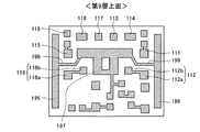
次に、積層体100に形成された導体パターンにつき、スイッチ回路SW1,SW2を中心として説明する。図5は積層体100の最上層である第9層の上面を示す説明図であり、図6は、最下層である第1層の下面、即ち、アンテナ切換モジュール10が備える積層体100の底面を表わしている。図7は積層体100の第9層の上面を覆うオーバコート層110の上面を示す説明図である。なお、図5,図6と後述する図8では、導体パターン,ビア電極を、それぞれ、右上がりの斜線ハッチング,右下がりの斜線ハッチングで表わすと共に、導体パターンの下に位置するビア電極の図示を省略している。
Next, the conductor pattern formed in the
図5に示すように、第9層の表面には、図4(A)に示した各種の実装部品の端子と導通される導体パターンが形成されている。この導体パターンには、ダイオードD2の入力端子に接続される端子パッド111と、ダイオードD2,SAWフィルタ121のそれぞれの端子に接続される端子パッド112と、SAWフィルタ121のSAWフィルタ回路SAW1側の出力端子に接続される端子パッド113,114と、抵抗器R2の出力端子およびダイオードD4の入力端子に接続される端子パッド115と、抵抗器R2の入力端子に接続される端子パッド119と、ダイオードD4,SAWフィルタ121のそれぞれの端子に接続される端子パッド116と、SAWフィルタ121のSAWフィルタ回路SAW2側の出力端子に接続される端子パッド117,118と、SAWフィルタ121のグランド端子に接続されるグランドパターン197とが含まれている。端子パッド112は、ダイオードD2の出力端子に接続される端子パッド112aと、SAWフィルタ121のSAWフィルタ回路SAW1側の入力端子に接続される端子パッド112bとを備えており、端子パッド116は、ダイオードD4の出力端子に接続される端子パッド116aと、SAWフィルタ121のSAWフィルタ回路SAW2側の入力端子に接続される端子パッド116bとを備えている。
As shown in FIG. 5, conductor patterns that are electrically connected to the terminals of the various mounting parts shown in FIG. 4A are formed on the surface of the ninth layer. The conductor pattern includes a
図6に示すように、積層体100の底面である第1層の下面には、図1のアンテナ切換回路AC1に示したアンテナ端子ANTと、送信端子TX1,TX2と、受信端子RX1a,RX1b,RX2a,RX2bと、制御端子VC1,VC2との他、グランドに接続されるグランド端子GND4,GND5,GND6とが設けられている。これらの端子は、積層体100の底面の互いに対向する2つの長辺に沿って、端子間の間隔をとりながら配置されている。一方の長辺側に配置された端子群と他方の長辺側に配置された端子群の間には、アンテナ切換モジュール10が実装された際にグランドに接続されるグランドパターン191,192,193,194が設けられている。
As shown in FIG. 6, on the lower surface of the first layer, which is the bottom surface of the laminate 100, the antenna terminal ANT shown in the antenna switching circuit AC1, the transmission terminals TX1 and TX2, and the reception terminals RX1a, RX1b, In addition to RX2a and RX2b and control terminals VC1 and VC2, ground terminals GND4, GND5 and GND6 connected to the ground are provided. These terminals are arranged along the two long sides facing each other on the bottom surface of the
ダイオードD2の入力端子に接続される端子パッド111は、積層体100内部の各層を介して、積層体100の底面の制御端子VC1に接続されている。制御端子VC1に対して制御電圧が印加されると、この電圧の印加によって生じたバイアス電流が端子パッド111に供給される。こうしたバイアス電流が端子パッド111を通じてダイオードD2の入力端子に入力されることにより、ダイオードD2が駆動(ON状態)する。これにより、アンテナに接続される信号経路が、送信端子TX1側から受信端子RX1a,RX1b側に切り換えられる。
The
抵抗器R2の出力端子およびダイオードD4の入力端子に接続される端子パッド115は、抵抗器R2,端子パッド119および積層体100内部の各層を介して、積層体100の底面の制御端子VC2に接続されている。制御端子VC2に対して制御電圧が印加されると、この電圧の印加によって生じたバイアス電流が端子パッド115に供給される。こうしたバイアス電流が端子パッド115を通じてダイオードD4の入力端子に入力されることによりダイオードD4が駆動(ON状態)する。これにより、アンテナに接続される信号経路が、送信端子TX2側から受信端子RX2a,RX2b側に切り換えられる。
The
SAWフィルタ121との接続用のグランドパターン197は、第9層の表面のほぼ中央部に設けられ、積層体100内部の各層を介してグランドに接続されている。このグランドパターン197は、第9層の表面において、その周縁の一部に設けられたシールドキャップ160用のグランドパターン196に、グランドパターン198を介して連結されている。この連結用のグランドパターン198は、連結対象となるグランドパターン196,197よりも狭い幅で、ダイオードD2との接続用の端子パッド111とダイオードD2およびSAWフィルタ121との接続用の端子パッド112の間を通って設けられている。また、SAWフィルタ121との接続用のグランドパターン197は、グランドパターン199を介して、第9層の表面のグランドパターン196に対向する周縁領域に設けられた、もう1つのシールドキャップ160用のグランドパターン195にも連結されている。この連結用のグランドパターン199は、グランドパターン198と同様に、連結対象となるグランドパターン195,197よりも狭い幅で、ダイオードD4との接続用の端子パッド115とダイオードD4およびSAWフィルタ121との接続用の端子パッド116の間を通って設けられている。
The
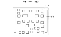
図7に示すように、オーバコート層110は、第9層の上面とほぼ同じ外形形状を有する。オーバコート層110には、複数の開口部OPTが設けられている。この複数の開口部OPTは、第9層の導体パターンに対応する位置に形成されている。
As shown in FIG. 7, the
オーバコート層110が第9層の上面にコーティングされたときの様子を図8に示した。なお、図8では、オーバコート層110に覆われた端子パッドを破線で表わすと共に、SAWフィルタ121、ダイオードD2,D4が実装される位置を二点鎖線で表わしている。図8に示すように、オーバコート層110が第9層の表面にコーティングされると、第9層の表面に形成されている導体パターンの一部がオーバコート層110の開口部OPTから露出した状態となる。この導体パターンのうちの端子パッドが露出した部分に、図4(A)に示した各種の実装部品の端子が半田付けによって実装される。こうした開口部OPTから露出した端子パッドには、図8に示すように、ダイオードD2の入力端子が装着される端子パッド111と、ダイオードD2の出力端子が装着される端子パッド112aと、SAWフィルタ121のSAWフィルタ回路SAW1側の入力端子が装着される端子パッド112bと、ダイオードD4の入力端子が装着される端子パッド115と、ダイオードD4の出力端子が装着される端子パッド116aと、SAWフィルタ121のSAWフィルタ回路SAW2側の入力端子が装着される端子パッド116bと、SAWフィルタ121のグランド端子が装着される端子パッドPG1a〜dとが含まれている。端子パッド111,端子パッド112aに、それぞれ、ダイオードD2の入力端子,出力端子が装着されると、ダイオードD2は連結用のグランドパターン198を跨ぐようにして実装される。また、端子パッド115,端子パッド116aに、それぞれ、ダイオードD4の入力端子,出力端子が装着されると、ダイオードD4は連結用のグランドパターン199を跨ぐようにして実装される。
A state when the
A−(4).アンテナ切換モジュール10の製造方法:
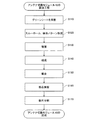
アンテナ切換モジュール10の製造方法について説明する。図9は、アンテナ切換モジュール10の製造工程の概略を示す説明図である。アンテナ切換モジュール10を製造する際には、始めに、誘電体材料の一つである低温焼成可能なガラスセラミックス材料から成るグリーンシートを複数用意する(工程S110)。グリーンシートの大きさは、複数個分の積層体100の大きさである。
A- (4). Manufacturing method of antenna switching module 10:
A method for manufacturing the
その後、各グリーンシートに、積層体100の隣接する各層を導通させるスルーホールと、アンテナ切換回路AC1を形成する導体パターンとを、積層体100の各層に対応させて形成する(工程S120)。スルーホールについては、スルーホールを形成する箇所に穴を開けた後、その穴に導体ペーストを充填させることによってビア電極を形成する。導体パターンについては、グリーンシートの表面に導体ペーストを印刷することによって形成する。なお、本実施例の導体ペーストの材料は、銀を主体とする材料を用いる。この工程において、積層体100の最下層表面や最上層表面に対応するグリーンシートには、既述した種々の接続端子や端子パッド111〜119、グランドパターン191〜199となる導体パターンが形成される。
Thereafter, a through hole for conducting each adjacent layer of the
導体パターンおよびビア電極を形成した後(工程S120)、積層体100の各層の導体パターンおよびビア電極が形成されたグリーンシートを、積層体100における各層の並びの順で積層する(工程S130)。この工程において、第9層に対応するグリーンシートには、図7に示したオーバコート層110がコーティングされる。オーバコート層110は、第9層と同様のアルミナを基調としたガラスセラミック材料から成る。
After forming the conductor pattern and the via electrode (step S120), the green sheet on which the conductor pattern and the via electrode of each layer of the laminate 100 are formed is laminated in the order of the layers in the laminate 100 (step S130). In this step, the
こうしてグリーンシートを積層した後(工程S130)、積層したグリーンシートを焼成する(工程S140)。その後、焼成したグリーンシートにおける各積層体100の表面に現れている導体パターンにニッケル−金メッキを施し(工程S150)、積層体100の最上層表面に、SAWフィルタ121やダイオードD2,D4等の実装部品やシールドキャップ160を半田付けする(工程S160)。この工程において、ダイオードD1,D2,D3,D4が極性の向きが同じ向きになるように実装され、ダイオードD2,D4が、それぞれ、連結用のグランドパターン198,199を跨ぐようにして実装される。その後、各積層体100を形成する個片毎に分割することで(工程S170)、アンテナ切換モジュール10が完成する。
After the green sheets are laminated in this way (step S130), the laminated green sheets are fired (step S140). Thereafter, the conductive pattern appearing on the surface of each laminate 100 in the fired green sheet is subjected to nickel-gold plating (step S150), and the
以上説明した本実施例のアンテナ切換モジュール10によれば、積層体100の最上面に、スイッチ回路SW1を構成する実装部品としてのダイオードD2を装着するための一対の端子パッド111,112aが設けられると共に、この一対の端子パッド111,112aの間の位置に、グランドに接続されるグランドパターン198が設けられている。これにより、ダイオードD2は、グランドパターン198を跨ぐようにして実装される。スイッチ回路SW2を構成する実装部品としてのダイオードD4も、ダイオードD2と同様に、グランドパターン199を跨ぐようにして実装される。このため、ダイオードD2,D4がバイアス電流を受けたことによってノイズが発生した場合に、このノイズは、ダイオードD2,D4が跨いでいるグランドパターン198,199に速やかに導かれる。従って、各スイッチ回路SW1,SW2での信号経路の切り換えに伴って発生したノイズを速やかに低減させることができる。
According to the
また、ダイオードD2,D4が跨いでいるグランドパターン198,199は、各グランドパターン198,199よりも大きな面積を有するSAWフィルタ121接続用のグランドパターン197に連結されることにより、それぞれ、SAWフィルタ121のグランド端子が装着される端子パッドPG1d,PG1aに接続されている。こうすれば、各グランドパターン198,199がグランドに接続される経路として、SAWフィルタ121接続用のグランドパターン197を介してグランドに接続される経路が増えるので、SAWフィルタ回路SAW1,SAW2のグランド電極のグランド電位が安定し、フィルタ特性が向上する。しかも、グランドパターン198,199が連結されるSAWフィルタ121接続用のグランドパターン197は、各グランドパターン198,199よりも大きな面積を有するので、SAWフィルタ回路SAW1,SAW2におけるグランド電位の安定度合いを更に高めることができる。
Further, the
更に、ダイオードD2,D4が跨いでいるグランドパターン198,199は、SAWフィルタ121の入力端子が装着される端子パッド112b,116bとダイオードD2,D4の入力端子が装着される端子パッド111,115の間に配置されている。従って、ダイオードD2,D4が端子パッド111,115を介してバイアス電流を受けたことによって発生したノイズが、SAWフィルタ121の入力側に回り込んでしまうことを防止することができる。
Furthermore, the
加えて、端子パッド111,115が受けたバイアス電流が、端子パッド111,115から他の端子(例えば、図8に示す端子パッド112a,116aや端子パッド112b,116b)に漏れた場合に、この漏れ信号は、ダイオードD2,D4が跨いでいるグランドパターン198,199に速やかに導かれる。従って、スイッチ回路での切り換えに際して受けたバイアス電流がパッド間で漏れてしまうことを防止することができる。
In addition, when the bias current received by the
本実施例のアンテナ切換モジュール10は、積層体100の最上面に装着されるシールドキャップ160は、互いに向かい合う縦方向の側壁163,165に付与された傾斜により、側壁163,165が有する端部167q,167sの近傍における収納部170の高さが端部167q,167sに近づくにつれて漸減されている。こうした形状のシールドキャップ160が装着される積層体100の最上面には、端部167s,端部167qが装着される周縁寄りの位置に、相対的に高さの低い実装部品(第1の部品群、第2の部品群)が配置されている。シールドキャップ160を装着したときに、周縁付近に実装された実装部品が、収納部170の高さを漸減させている側壁163,165に干渉しにくくなり、実装部品とシールドキャップ160との干渉によって生じ得る種々の不具合(例えば、実装部品と導体パターンとの接続不良や実装部品自体の破損)を回避することができる。
In the
本実施例のアンテナ切換モジュール10では、積層体100の最上面に、4つのダイオードD1,D2,D3,D4が、極性の向きが同じ向きになるように実装されるので、製造段階でのダイオードの誤った実装を回避し易くなる。また、4つのダイオードD1,D2,D3,D4は樹脂モールドされているので、ダイオードの強度を確保することができる。
In the
B.その他の実施形態:
以上、本発明の実施の形態について説明したが、本発明はこうした実施の形態に何ら限定されるものではなく、本発明の趣旨を逸脱しない範囲内において様々な形態で実施し得ることは勿論である。例えば、アンテナ切換モジュールが対応する通信システムは、デュアルに限るものではなく、トリプルバンドやクワッドバンド、更に5つ以上の通信方式に対応するものに適用できることは勿論である。また、上記実施例では、積層体100に、GSMおよびDCSの2つの通信システムのそれぞれに対応したアンテナ切換回路AC1を形成したが、1つの通信システムに対応したアンテナ切換回路AC1を積層体100に形成することとしても差し支えない。
B. Other embodiments:
As mentioned above, although embodiment of this invention was described, this invention is not limited to such embodiment at all, Of course, it can implement with various forms within the range which does not deviate from the meaning of this invention. is there. For example, the communication system supported by the antenna switching module is not limited to the dual, but can be applied to a triple band, quad band, or a communication system corresponding to five or more communication methods. Moreover, in the said Example, although the antenna switching circuit AC1 corresponding to each of the two communication systems of GSM and DCS was formed in the
上記実施例において、各接続端子の並設の順序は、実施例の順序に限定されるものではなく、本発明の範囲を逸脱しない範囲で適宜変更することができる。また、並設された送信端子と受信端子との間のグランドパターンや各接続端子の形状・大きさは、実施例のものに限定するものではなく、円形や多角形など種々の態様を採ることができる。 In the above-described embodiment, the order in which the connection terminals are arranged in parallel is not limited to the order of the embodiments, and can be changed as appropriate without departing from the scope of the present invention. In addition, the ground pattern between the transmission terminal and the reception terminal arranged in parallel and the shape and size of each connection terminal are not limited to those of the embodiment, and various forms such as a circle and a polygon are adopted. Can do.
上記実施例において説明した製造工程において、各接続端子やグランドパターンを、積層工程前のグリーンシートに形成するのではなく、焼成後に形成することとしても良い。また、積層工程(図9の工程S130)において、オーバコート層110によるコーティングをしないこととしても差し支えない。
In the manufacturing process described in the above embodiment, each connection terminal and ground pattern may be formed after firing instead of being formed on the green sheet before the lamination process. Further, in the stacking step (step S130 in FIG. 9), the
上記実施例では、スイッチ回路に用いるスイッチング素子をダイオードとしたが、ダイオード以外のスイッチング素子(例えば、GaAs(ガリウム・ヒ素)スイッチ)を用いてスイッチ回路を構成することも可能である。こうしたスイッチング素子を駆動させるトリガーとしては、上記実施例のようなバイアス電流のほか、各種の電気信号や磁気信号等、ノイズの発生源となり得る種々の信号を考えることができる。 In the above embodiment, the switching element used in the switch circuit is a diode, but it is also possible to configure the switch circuit using a switching element other than the diode (for example, a GaAs (gallium arsenide) switch). As a trigger for driving such a switching element, in addition to the bias current as in the above-described embodiment, various signals that can be sources of noise such as various electric signals and magnetic signals can be considered.
上記実施例では、シールドキャップ160を、実装部品の配置が予定されていない部位である「積層体100の最上面の周縁」に装着したが、実装部品の配置が予定されていない他の部位にシールドキャップ160を装着してもよい。こうした他の部位としては、例えば、積層体100の側面などを考えることができる。
In the above embodiment, the
更に、上記実施例では、ローパスフィルタ回路LPF3、ダイプレクサ回路DP、スイッチ回路SW1、SAWフィルタ回路SAW1、ローパスフィルタ回路LPF1、スイッチ回路SW2、SAWフィルタ回路SAW2、ローパスフィルタ回路LPF2から構成されるアンテナ切換回路AC1を1つの積層体100に形成したが、上記のアンテナ切換回路AC1を構成する一部の回路のみを1つの積層体に形成することとしても差し支えない。この場合には、上記の各回路を複数の積層体に分けて形成しておき、積層体同士を導通可能に接続すれば、上記実施例のアンテナ切換モジュール10と同様の機能を実現することができる。
Further, in the above embodiment, the antenna switching circuit including the low-pass filter circuit LPF3, the diplexer circuit DP, the switch circuit SW1, the SAW filter circuit SAW1, the low-pass filter circuit LPF1, the switch circuit SW2, the SAW filter circuit SAW2, and the low-pass filter circuit LPF2. Although AC1 is formed in one
10,10A,10B,10C...アンテナ切換モジュール
100...積層体
101...第1長辺部
102...第2長辺部
103...第1短辺部
104...第2短辺部
110...オーバコート層
111〜119...端子パッド
121...SAWフィルタ
131,D1,D2,D3,D4...ダイオード
141,L9,L10,L11...コイル
151,R1,R2...抵抗器
160...シールドキャップ
161...天壁
161a...表面
161b...裏面
162〜165...側壁
162a〜165a...表面
162b〜165b...裏面
167、167p〜s...端部
170...収納部
191〜199...グランドパターン
AC1...アンテナ切換回路
ANT...アンテナ端子
C10...コンデンサ
DP...ダイプレクサ回路
GND4〜6...グランド端子
LPF1,LPF2,LPF3...ローパスフィルタ回路
SW1,SW2...スイッチ回路
OPT...開口部
PG1a〜d...端子パッド
RX1a,RX1b,RX2a,RX2b...受信端子
SAW1,SAW2...SAWフィルタ回路
TX1,TX2...送信端子
VC1,VC2...制御端子
10, 10A, 10B, 10C ...
Claims (10)
前記アンテナ切換回路は、所定の信号を受けて駆動するスイッチング素子の駆動状態を変更することにより、前記アンテナと前記送信回路または前記受信回路のいずれかに接続を切り換えるスイッチ回路を備え、
前記積層体の表面には、前記スイッチング素子が有する端子と導通するための少なくとも一対のスイッチング素子用端子パッドが設けられると共に、該一対のスイッチング素子用端子パッドの間の位置に、グランドに接続されるグランドパターンが設けられており、
前記スイッチング素子は、前記端子を前記スイッチング素子用端子パッドに接続することにより、前記グランドパターンを跨ぐようにして実装された
アンテナ切換モジュール。 At least a part of an antenna switching circuit that switches connection between a transmission circuit and a reception circuit corresponding to a communication system of a predetermined communication frequency band and an antenna that transmits and receives communication radio waves is provided in a laminate in which dielectric ceramic layers are laminated. An antenna switching module,
The antenna switching circuit includes a switch circuit that switches a connection between the antenna and the transmission circuit or the reception circuit by changing a driving state of a switching element that receives and drives a predetermined signal.
On the surface of the laminate, at least a pair of switching element terminal pads are provided for electrical connection with the terminals of the switching elements, and connected to the ground at a position between the pair of switching element terminal pads. Ground pattern is provided,
The switching element is mounted so as to straddle the ground pattern by connecting the terminal to the switching element terminal pad.
前記アンテナ切換回路は、特定の周波数帯域の信号を通過させるフィルタ回路を備え、
該フィルタ回路は、前記スイッチ回路と前記受信回路との間に接続され、
前記積層体の表面には、前記フィルタ回路が形成されたフィルタ素子が実装され、
前記積層体の表面には、該フィルタ素子が有する端子と導通するための少なくとも一つのフィルタ回路用端子パッドが形成され、
該フィルタ回路用端子パッドのうち、グランドに接続される端子パッドと前記グランドパターンとが接続されている
アンテナ切換モジュール。 The antenna switching module according to claim 1,
The antenna switching circuit includes a filter circuit that passes a signal of a specific frequency band,
The filter circuit is connected between the switch circuit and the receiving circuit,
A filter element in which the filter circuit is formed is mounted on the surface of the laminate,
On the surface of the laminate, at least one filter circuit terminal pad is formed for electrical connection with a terminal of the filter element,
Of the filter circuit terminal pads, a terminal pad connected to the ground and the ground pattern are connected to the antenna switching module.
前記アンテナ切換回路は、通信周波数帯域の異なる複数の通信システムのそれぞれに対応する前記送信回路および前記受信回路と前記アンテナとの接続を切り換える回路であり、
前記アンテナ切換回路は、前記複数の通信システムのそれぞれに対応する送信回路および受信回路ごとに、別々の前記スイッチ回路を備えており、
前記スイッチング素子用端子パッドは、前記別々のスイッチ回路のそれぞれが備える前記スイッチング素子の端子との導通に対応して、前記積層体の表面の複数の箇所に設けられており、
前記それぞれのスイッチング素子が、対応する前記スイッチング素子用端子パッドへの接続によって、前記グランドパターンを跨ぐように実装された
アンテナ切換モジュール。 The antenna switching module according to claim 1 or 2,
The antenna switching circuit is a circuit that switches the connection between the transmission circuit and the reception circuit and the antenna corresponding to each of a plurality of communication systems having different communication frequency bands,
The antenna switching circuit includes a separate switch circuit for each of a transmission circuit and a reception circuit corresponding to each of the plurality of communication systems,
The switching element terminal pads are provided at a plurality of locations on the surface of the multilayer body, corresponding to conduction with the terminals of the switching elements included in each of the separate switch circuits,
An antenna switching module, wherein each switching element is mounted so as to straddle the ground pattern by connection to the corresponding switching element terminal pad.
前記アンテナ切換回路は、特定の周波数帯域の信号を通過させるフィルタ回路を複数備えており、該複数のフィルタ回路のそれぞれは、前記別々の各スイッチ回路とそれぞれのスイッチ回路に対応した受信回路との間に接続され、
前記積層体の表面には、前記複数の各フィルタ回路が形成された複数の各フィルタ素子が実装され、
前記積層体の表面には、各フィルタ素子が有する端子と導通するための少なくとも一つのフィルタ回路用端子パッドが形成され、
該フィルタ回路用端子パッドのうち、グランドに接続される端子パッドと前記グランドパターンとが接続されている
アンテナ切換モジュール。 The antenna switching module according to claim 3,
The antenna switching circuit includes a plurality of filter circuits that allow a signal in a specific frequency band to pass, and each of the plurality of filter circuits includes a separate switch circuit and a reception circuit corresponding to the switch circuit. Connected between and
A plurality of filter elements in which the plurality of filter circuits are formed are mounted on the surface of the laminate,
On the surface of the laminate, at least one filter circuit terminal pad is formed for electrical connection with a terminal of each filter element,
Of the filter circuit terminal pads, a terminal pad connected to the ground and the ground pattern are connected to the antenna switching module.
前記積層体の表面に実装された複数の素子を収納する収納部と前記積層体の周縁に装着される端部とを備えたシールドキャップを備え、
該シールドキャップは、前記端部の近傍における前記収納部の高さが該端部に近づくにつれて漸減された形状を有しており、
前記積層体の表面には、その近傍における収納部の高さが漸減されている前記端部が装着される前記周縁寄りの位置に、相対的に高さの低い前記素子が実装されている
アンテナ切換モジュール。 The antenna switching module according to any one of claims 1 to 4,
A shield cap including a storage portion for storing a plurality of elements mounted on the surface of the laminate, and an end attached to the periphery of the laminate,
The shield cap has a shape in which the height of the storage portion in the vicinity of the end portion is gradually reduced as it approaches the end portion,
The element having a relatively low height is mounted on the surface of the laminated body at a position near the peripheral edge where the end portion where the height of the storage portion in the vicinity thereof is gradually reduced is mounted. Antenna Switching module.
前記アンテナ切換回路は、所定の信号の入力によってスイッチング素子を駆動させることにより、前記アンテナに接続される回路を前記送信回路または前記受信回路のいずれかに切り換えるスイッチ回路を備え、
前記積層体の表面には、前記スイッチング素子が有する端子に導通するための端子パッドが設けられており、
前記端子パッドのうち前記所定の信号が通過する端子パッドと、それ以外のパッドとの間に、グランドに接続されるグランドパターンが設けられている
積層体。 Formed by laminating dielectric ceramic layers, at least part of an antenna switching circuit for switching connection between a transmission circuit and a reception circuit corresponding to a communication system of a predetermined communication frequency band and an antenna for transmitting and receiving communication radio waves is formed A laminated body comprising:
The antenna switching circuit includes a switch circuit that switches a circuit connected to the antenna to either the transmission circuit or the reception circuit by driving a switching element by inputting a predetermined signal.
The surface of the laminate is provided with a terminal pad for conducting to the terminal of the switching element,
A laminate in which a ground pattern connected to the ground is provided between a terminal pad through which the predetermined signal passes among the terminal pads and the other pads.
前記アンテナ切換回路は、所定の信号の入力によってスイッチング素子を駆動させることにより、前記アンテナに接続される回路を前記送信回路または前記受信回路のいずれかに切り換えるスイッチ回路を備え、
前記積層体の表面には、前記スイッチング素子が有する端子に接続される複数個の端子パッドが設けられており、
該複数個の端子パッドの間に、グランドに接続されるグランドパターンを設けた
積層体。 Formed by laminating dielectric ceramic layers, at least part of an antenna switching circuit for switching connection between a transmission circuit and a reception circuit corresponding to a communication system of a predetermined communication frequency band and an antenna for transmitting and receiving communication radio waves is formed A laminated body comprising:
The antenna switching circuit includes a switch circuit that switches a circuit connected to the antenna to either the transmission circuit or the reception circuit by driving a switching element by inputting a predetermined signal.
A plurality of terminal pads connected to the terminals of the switching element are provided on the surface of the laminate,
A laminate in which a ground pattern connected to the ground is provided between the plurality of terminal pads.
Priority Applications (1)
| Application Number | Priority Date | Filing Date | Title |
|---|---|---|---|
| JP2004109681A JP2005295350A (en) | 2004-04-02 | 2004-04-02 | Antenna switching module and laminate for forming antenna switching circuit |
Applications Claiming Priority (1)
| Application Number | Priority Date | Filing Date | Title |
|---|---|---|---|
| JP2004109681A JP2005295350A (en) | 2004-04-02 | 2004-04-02 | Antenna switching module and laminate for forming antenna switching circuit |
Publications (1)
| Publication Number | Publication Date |
|---|---|
| JP2005295350A true JP2005295350A (en) | 2005-10-20 |
Family
ID=35327769
Family Applications (1)
| Application Number | Title | Priority Date | Filing Date |
|---|---|---|---|
| JP2004109681A Pending JP2005295350A (en) | 2004-04-02 | 2004-04-02 | Antenna switching module and laminate for forming antenna switching circuit |
Country Status (1)
| Country | Link |
|---|---|
| JP (1) | JP2005295350A (en) |
Cited By (2)
| Publication number | Priority date | Publication date | Assignee | Title |
|---|---|---|---|---|
| US8660603B2 (en) | 2006-03-31 | 2014-02-25 | Epcos Ag | Mobile radio module for multiband-multimode operation |
| JPWO2012117992A1 (en) * | 2011-03-02 | 2014-07-07 | 株式会社村田製作所 | High frequency module |
Citations (3)
| Publication number | Priority date | Publication date | Assignee | Title |
|---|---|---|---|---|
| JP2000049651A (en) * | 1998-07-27 | 2000-02-18 | Hitachi Metals Ltd | High frequency switch module for multi-band |
| JP2001352269A (en) * | 2000-06-09 | 2001-12-21 | Hitachi Metals Ltd | High frequency switch module |
| JP2002158449A (en) * | 2000-11-22 | 2002-05-31 | Tdk Corp | High-frequency electronic circuit module and multilayer board therefor |
-
2004
- 2004-04-02 JP JP2004109681A patent/JP2005295350A/en active Pending
Patent Citations (3)
| Publication number | Priority date | Publication date | Assignee | Title |
|---|---|---|---|---|
| JP2000049651A (en) * | 1998-07-27 | 2000-02-18 | Hitachi Metals Ltd | High frequency switch module for multi-band |
| JP2001352269A (en) * | 2000-06-09 | 2001-12-21 | Hitachi Metals Ltd | High frequency switch module |
| JP2002158449A (en) * | 2000-11-22 | 2002-05-31 | Tdk Corp | High-frequency electronic circuit module and multilayer board therefor |
Cited By (2)
| Publication number | Priority date | Publication date | Assignee | Title |
|---|---|---|---|---|
| US8660603B2 (en) | 2006-03-31 | 2014-02-25 | Epcos Ag | Mobile radio module for multiband-multimode operation |
| JPWO2012117992A1 (en) * | 2011-03-02 | 2014-07-07 | 株式会社村田製作所 | High frequency module |
Similar Documents
| Publication | Publication Date | Title |
|---|---|---|
| US9160304B2 (en) | Branching filter and communication module component | |
| JP3818896B2 (en) | Demultiplexer and electronic device using the same | |
| US9252476B2 (en) | Circuit module including a splitter and a mounting substrate | |
| US9413413B2 (en) | High-frequency module | |
| JP2005268878A (en) | Antenna duplexer | |
| US11742821B2 (en) | Multiplexer, filter, and communication module | |
| JP4166635B2 (en) | Multilayer high frequency module | |
| JP3925771B2 (en) | High frequency switch module | |
| JP2005260837A (en) | Antenna switching module and design method thereof | |
| US20140179364A1 (en) | Circuit module | |
| US7183878B2 (en) | Surface acoustic wave filter | |
| JP2005295350A (en) | Antenna switching module and laminate for forming antenna switching circuit | |
| JP2005311929A (en) | Antenna switching module | |
| JP4177282B2 (en) | Antenna switching module | |
| JP4596300B2 (en) | High frequency switch module | |
| JP3806719B2 (en) | Antenna switching module and manufacturing method thereof | |
| JP4006698B2 (en) | Dual band transceiver | |
| JP2001352272A (en) | High frequency switch module | |
| JPH10276117A (en) | Composite switch circuit parts | |
| JP4565368B2 (en) | High frequency switch module | |
| JP4331634B2 (en) | Antenna switching module and manufacturing method thereof | |
| JP3838438B2 (en) | Composite switch circuit parts | |
| JP4135936B2 (en) | High frequency module and high frequency circuit | |
| JP2005295479A (en) | Antenna switching module | |
| JP2005039407A (en) | Branching filter |
Legal Events
| Date | Code | Title | Description |
|---|---|---|---|
| A977 | Report on retrieval |
Free format text: JAPANESE INTERMEDIATE CODE: A971007 Effective date: 20070717 |
|
| A131 | Notification of reasons for refusal |
Free format text: JAPANESE INTERMEDIATE CODE: A131 Effective date: 20071016 |
|
| A02 | Decision of refusal |
Free format text: JAPANESE INTERMEDIATE CODE: A02 Effective date: 20080304 |