JP2005295322A - Package, piezoelectric device and manufacturing method thereof - Google Patents
Package, piezoelectric device and manufacturing method thereof Download PDFInfo
- Publication number
- JP2005295322A JP2005295322A JP2004109165A JP2004109165A JP2005295322A JP 2005295322 A JP2005295322 A JP 2005295322A JP 2004109165 A JP2004109165 A JP 2004109165A JP 2004109165 A JP2004109165 A JP 2004109165A JP 2005295322 A JP2005295322 A JP 2005295322A
- Authority
- JP
- Japan
- Prior art keywords
- substrate
- package
- hole
- vibrating piece
- connecting portion
- Prior art date
- Legal status (The legal status is an assumption and is not a legal conclusion. Google has not performed a legal analysis and makes no representation as to the accuracy of the status listed.)
- Pending
Links
- 238000004519 manufacturing process Methods 0.000 title claims abstract description 24
- 239000000758 substrate Substances 0.000 claims abstract description 244
- 238000007789 sealing Methods 0.000 claims abstract description 39
- 238000010438 heat treatment Methods 0.000 claims abstract description 25
- 238000000034 method Methods 0.000 claims abstract description 21
- 238000007872 degassing Methods 0.000 claims abstract description 17
- 230000000149 penetrating effect Effects 0.000 claims abstract description 8
- 229910052751 metal Inorganic materials 0.000 claims description 41
- 239000002184 metal Substances 0.000 claims description 41
- 238000000465 moulding Methods 0.000 claims description 12
- 230000001678 irradiating effect Effects 0.000 claims description 8
- 238000004891 communication Methods 0.000 claims description 4
- 239000003566 sealing material Substances 0.000 description 24
- 239000000463 material Substances 0.000 description 17
- WFKWXMTUELFFGS-UHFFFAOYSA-N tungsten Chemical compound [W] WFKWXMTUELFFGS-UHFFFAOYSA-N 0.000 description 8
- 229910052721 tungsten Inorganic materials 0.000 description 8
- 239000010937 tungsten Substances 0.000 description 8
- 239000000853 adhesive Substances 0.000 description 7
- 230000001070 adhesive effect Effects 0.000 description 7
- 230000005284 excitation Effects 0.000 description 7
- 238000005520 cutting process Methods 0.000 description 6
- 230000015572 biosynthetic process Effects 0.000 description 5
- 238000001465 metallisation Methods 0.000 description 5
- 238000009423 ventilation Methods 0.000 description 5
- 238000010030 laminating Methods 0.000 description 4
- 230000002093 peripheral effect Effects 0.000 description 4
- 238000007639 printing Methods 0.000 description 4
- 239000010453 quartz Substances 0.000 description 4
- VYPSYNLAJGMNEJ-UHFFFAOYSA-N silicon dioxide Inorganic materials O=[Si]=O VYPSYNLAJGMNEJ-UHFFFAOYSA-N 0.000 description 4
- 238000005245 sintering Methods 0.000 description 4
- 239000011230 binding agent Substances 0.000 description 3
- 239000011248 coating agent Substances 0.000 description 3
- 238000000576 coating method Methods 0.000 description 3
- 239000010931 gold Substances 0.000 description 3
- 238000002844 melting Methods 0.000 description 3
- 230000008018 melting Effects 0.000 description 3
- 238000007747 plating Methods 0.000 description 3
- 229920003002 synthetic resin Polymers 0.000 description 3
- 239000000057 synthetic resin Substances 0.000 description 3
- 229910017401 Au—Ge Inorganic materials 0.000 description 2
- 101000911772 Homo sapiens Hsc70-interacting protein Proteins 0.000 description 2
- PXHVJJICTQNCMI-UHFFFAOYSA-N Nickel Chemical compound [Ni] PXHVJJICTQNCMI-UHFFFAOYSA-N 0.000 description 2
- 239000000919 ceramic Substances 0.000 description 2
- 239000011651 chromium Substances 0.000 description 2
- 230000005684 electric field Effects 0.000 description 2
- 238000000605 extraction Methods 0.000 description 2
- 239000000945 filler Substances 0.000 description 2
- 238000011049 filling Methods 0.000 description 2
- 238000010304 firing Methods 0.000 description 2
- 239000011521 glass Substances 0.000 description 2
- PCHJSUWPFVWCPO-UHFFFAOYSA-N gold Chemical compound [Au] PCHJSUWPFVWCPO-UHFFFAOYSA-N 0.000 description 2
- 229910052737 gold Inorganic materials 0.000 description 2
- 238000005304 joining Methods 0.000 description 2
- 239000000155 melt Substances 0.000 description 2
- 239000002245 particle Substances 0.000 description 2
- 238000003825 pressing Methods 0.000 description 2
- WSMQKESQZFQMFW-UHFFFAOYSA-N 5-methyl-pyrazole-3-carboxylic acid Chemical compound CC1=CC(C(O)=O)=NN1 WSMQKESQZFQMFW-UHFFFAOYSA-N 0.000 description 1
- VYZAMTAEIAYCRO-UHFFFAOYSA-N Chromium Chemical compound [Cr] VYZAMTAEIAYCRO-UHFFFAOYSA-N 0.000 description 1
- 101001139126 Homo sapiens Krueppel-like factor 6 Proteins 0.000 description 1
- BQCADISMDOOEFD-UHFFFAOYSA-N Silver Chemical compound [Ag] BQCADISMDOOEFD-UHFFFAOYSA-N 0.000 description 1
- 238000000137 annealing Methods 0.000 description 1
- 239000005388 borosilicate glass Substances 0.000 description 1
- 229910052804 chromium Inorganic materials 0.000 description 1
- 238000005530 etching Methods 0.000 description 1
- 239000000835 fiber Substances 0.000 description 1
- 238000007689 inspection Methods 0.000 description 1
- 239000011810 insulating material Substances 0.000 description 1
- GQYHUHYESMUTHG-UHFFFAOYSA-N lithium niobate Chemical compound [Li+].[O-][Nb](=O)=O GQYHUHYESMUTHG-UHFFFAOYSA-N 0.000 description 1
- 238000010295 mobile communication Methods 0.000 description 1
- 229910052759 nickel Inorganic materials 0.000 description 1
- 239000011224 oxide ceramic Substances 0.000 description 1
- 229910052574 oxide ceramic Inorganic materials 0.000 description 1
- TWNQGVIAIRXVLR-UHFFFAOYSA-N oxo(oxoalumanyloxy)alumane Chemical compound O=[Al]O[Al]=O TWNQGVIAIRXVLR-UHFFFAOYSA-N 0.000 description 1
- 239000004033 plastic Substances 0.000 description 1
- 238000006116 polymerization reaction Methods 0.000 description 1
- 239000000843 powder Substances 0.000 description 1
- 238000004080 punching Methods 0.000 description 1
- 229910052709 silver Inorganic materials 0.000 description 1
- 239000004332 silver Substances 0.000 description 1
- 239000012780 transparent material Substances 0.000 description 1
Images


Landscapes
- Piezo-Electric Or Mechanical Vibrators, Or Delay Or Filter Circuits (AREA)
Abstract
【課題】 脱ガス用の孔を封止する際に、加熱用ビームをパッケージ内に侵入させることがなく、周波数シフトが生じることを有効に防止できるパッケージと、圧電デバイス、および圧電デバイスの製造方法を提供すること。
【解決手段】 パッケージ37内に圧電振動片32を収容して、このパッケージを気密に封止した圧電デバイス30であって、前記パッケージが複数層の絶縁基板を積層した底部を有しており、最も外側に位置する第1の基板55には、外部に開いた貫通孔62が形成されていて、前記第1の基板に重ねられた第2の基板56には、前記貫通孔の一部と重なる箇所を基端として基板平面に沿って延びる細い幅の連絡部63が形成されており、前記連絡部は、基端側が前記貫通孔と連通した有底の溝であり、延長端側が前記パッケージ内部に開口している貫通部64を備えている。
【選択図】 図2
PROBLEM TO BE SOLVED: To provide a package capable of effectively preventing a frequency shift without causing a heating beam to enter the package when sealing a degassing hole, a piezoelectric device, and a method for manufacturing the piezoelectric device To provide.
A piezoelectric device 30 in which a piezoelectric vibrating piece 32 is housed in a package 37 and the package is hermetically sealed, the package having a bottom portion on which a plurality of insulating substrates are stacked, A through hole 62 opened to the outside is formed in the first substrate 55 located on the outermost side, and a part of the through hole is formed on the second substrate 56 superimposed on the first substrate. A connecting portion 63 having a narrow width extending along the substrate plane with the overlapping portion as a base end is formed. The connecting portion is a bottomed groove whose base end side communicates with the through hole, and the extended end side is the package. A penetrating portion 64 opened inside is provided.
[Selection] Figure 2
Description
本発明は、パッケージと、パッケージ内に圧電振動片を収容した圧電デバイスおよびその製造方法に関する。 The present invention relates to a package, a piezoelectric device in which a piezoelectric vibrating piece is accommodated in the package, and a manufacturing method thereof.
HDD(ハード・ディスク・ドライブ)、モバイルコンピュータ、あるいはICカード等の小型の情報機器や、携帯電話、自動車電話、またはページングシステム等の移動体通信機器において、圧電振動子や圧電発振器等の圧電デバイスが広く使用されている。
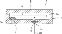
従来の表面実装型の圧電デバイスは、例えば、図9の概略断面図に示すように構成されている(特許文献1参照)。
Piezoelectric devices such as piezoelectric vibrators and piezoelectric oscillators in small information devices such as HDDs (hard disk drives), mobile computers, IC cards, and mobile communication devices such as mobile phones, car phones, and paging systems Is widely used.
A conventional surface-mount type piezoelectric device is configured, for example, as shown in a schematic cross-sectional view of FIG. 9 (see Patent Document 1).
図において、圧電デバイス1は、セラミック製の浅い箱状のパッケージ2内に電極部4を形成し、この電極部4に導電性接着剤4aを用いて、圧電振動片3を固定している。このパッケージ2は、蓋体5により気密に封止されている。
パッケージ2の底部には、貫通孔6が形成されており、蓋体5の封止に際して、真空雰囲気下において、封止材5aが加熱されると、例えば、導電性接着剤4a等から生成されるガス成分がこの貫通孔6からパッケージ2の外部に排出される。これにより、有害なガス成分が圧電振動片3に付着して、周波数をシフトさせることなどが、防止されている。
In the figure, the
A through-
ここで、貫通孔6を利用した上記脱ガス工程の後で、貫通孔6の段部には、金属ボールが配置され、レーザ光LB等のような加熱用ビームを用いて、この金属ボールを溶融することによる充填材6aで貫通孔6を塞ぎ、孔封止を行うようにしている。
Here, after the degassing step using the through-
ところが、パッケージ2に形成された貫通孔6は、パッケージ2のほぼ中心付近に形成されている。
このため、金属ボールにレーザ光LBを照射して、充填材6aとする際に、レーザ光LBが短時間でも金属ボールを溶かしながらパッケージ2内部に点線で示すように透過してしまうと、圧電振動片3自体の下面に照射されてしまう。
このパッケージ2内に侵入したレーザ光LBは、圧電振動片3の電極などの金属膜を部分的に蒸散させてしまうおそれがあり、その場合には、圧電振動片3の周波数がシフトするおそれがある。
However, the
For this reason, when the metal ball is irradiated with the laser beam LB to form the
The laser beam LB that has entered the
本発明は、以上の課題を解決するためになされたもので、脱ガス用の孔を封止する際に、加熱用ビームをパッケージ内に侵入させることがなく、周波数シフトが生じることを有効に防止できるパッケージと、圧電デバイス、および圧電デバイスの製造方法を提供することを目的とする。 The present invention has been made to solve the above-described problems, and effectively seals a degassing hole without causing a heating beam to enter the package and causing a frequency shift. An object of the present invention is to provide a package that can be prevented, a piezoelectric device, and a method for manufacturing the piezoelectric device.
上述の目的は、第1の発明にあっては、パッケージ内に圧電振動片を収容して、このパッケージを気密に封止した圧電デバイスであって、前記パッケージが複数層の絶縁基板を積層した底部を有しており、最も外側に位置する第1の基板には、外部に開いた貫通孔が形成されていて、前記第1の基板に重ねられた第2の基板には、前記貫通孔の一部と重なる箇所を基端として基板平面に沿って延びる細い幅の連絡部が形成されており、前記連絡部は、基端側が前記貫通孔と連通した有底の溝であり、延長端側が前記パッケージ内部に開口している貫通部を備えている圧電デバイスにより、達成される。
第1の発明の構成によれば、前記パッケージ内部は第2の基板に形成した前記貫通部から、前記細い幅の連絡部を通り前記第1の基板の貫通孔とつながっており、外部と通気できるようにされている。これにより、脱ガスの工程では、パッケージ内部のガスは前記第2の基板の貫通部、細い幅の連絡部、第1の基板の貫通孔をそれぞれ通過して、パッケージの外部に排出される。
また、前記第1の基板の外部に開いた前記貫通孔を金属封止材により封止する際に、この貫通孔に臨ませてリジットな金属封止材を配置した状態においては、この金属封止材にレーザ等の加熱ビームを照射して溶融させる場合に、加熱ビームは金属封止材の溶融の際に第2の基板を貫通することができないから、加熱ビームがパッケージ内部に侵入することがなく、圧電振動片に照射されるおそれがない。このため、周波数をシフトさせることがない。しかも、第1の基板の貫通孔とパッケージ内部とをつなぐ部分は、細い幅の連絡部とされることにより、大きなスリットや開口とする場合に比べて、パッケージ底部の強度を十分に確保して、通気構造を実現できる。
According to the first aspect of the present invention, there is provided a piezoelectric device in which a piezoelectric vibrating piece is accommodated in a package and the package is hermetically sealed, and the package is formed by laminating a plurality of insulating substrates. The first substrate which has a bottom and is located on the outermost side is formed with a through hole opened to the outside, and the second substrate overlaid on the first substrate has the through hole A connecting portion having a narrow width extending along the substrate plane with a portion overlapping with a part of the connecting portion being formed as a base end, the connecting portion being a bottomed groove having a base end side communicating with the through hole, and an extension end This is achieved by a piezoelectric device having a through-side that opens into the package.
According to the configuration of the first invention, the inside of the package is connected to the through hole of the first substrate from the through portion formed in the second substrate, through the narrow connecting portion, and vented to the outside. It has been made possible. As a result, in the degassing step, the gas inside the package passes through the through portion of the second substrate, the narrow connecting portion, and the through hole of the first substrate, and is discharged to the outside of the package.
In addition, when the through hole opened to the outside of the first substrate is sealed with a metal sealing material, in the state where a rigid metal sealing material is disposed facing the through hole, the metal sealing is performed. When the stop material is irradiated with a heating beam such as a laser and melted, the heating beam cannot penetrate the second substrate when the metal sealing material is melted. There is no risk of irradiating the piezoelectric vibrating piece. For this reason, the frequency is not shifted. Moreover, the portion connecting the through hole of the first substrate and the inside of the package is a narrow connecting portion, so that the strength of the bottom of the package is sufficiently ensured as compared with the case of a large slit or opening. A ventilation structure can be realized.
上述の目的は、第2の発明にあっては、パッケージ内に圧電振動片を収容して、このパッケージを気密に封止した圧電デバイスであって、前記パッケージが複数層の絶縁基板を積層した底部を有しており、前記底部を構成する複数層の前記絶縁基板として、少なくとも第1ないし第3の3枚の基板を有しており、最も外側に位置する第1の基板には、外部に開いた貫通孔が形成されていて、前記第1の基板に重ねられた第2の基板には、前記貫通孔の一部と重なる箇所を基端として基板平面に沿って延びる細い幅の連絡部が形成されており、前記第2の基板に重ねられる第3の基板には、前記貫通孔と重ならない位置に前記パッケージ内部に開口する開口部が形成され、かつ前記連絡部は、基端側が前記貫通孔と連通し、延長端側が前記開口部と連通する構成とした圧電デバイスにより、達成される。
第2の発明の構成によれば、前記パッケージ内部は第3の基板の前記開口部から、前記第2の基板の細い幅の連絡部を通り前記第1の基板の貫通孔とつながっており、外部と通気できるようにされている。これにより、脱ガスの工程では、パッケージ内部のガスは前記第3の基板の開口部、第2の基板の細い幅の連絡部、第1の基板の貫通孔をそれぞれ通過して、パッケージの外部に排出される。
また、前記第1の基板の外部に開いた前記貫通孔を金属封止材により封止する際に、この貫通孔に臨ませてリジットな金属封止材を配置した状態においては、この金属封止材にレーザ等の加熱ビームを照射して溶融させる場合に、加熱ビームは金属封止材の溶融の際に第2の基板を貫通することができないから、加熱ビームがパッケージ内部に侵入することがなく、圧電振動片に照射されるおそれがない。このため、周波数をシフトさせることがない。しかも、第1の基板の貫通孔と第3の基板の前記開口部を介して、パッケージ内部とをつなぐ部分は、細い幅の連絡部とされることにより、大きなスリットや開口とする場合に比べて、パッケージ底部の強度を十分に確保して、通気構造を実現できる。
According to the second aspect of the present invention, there is provided a piezoelectric device in which a piezoelectric vibrating piece is accommodated in a package and the package is hermetically sealed, and the package is formed by laminating a plurality of insulating substrates. The first substrate having at least the first to third substrates as the plurality of layers of the insulating substrates constituting the bottom portion, and the outermost first substrate being external A through hole that is open to the first substrate is formed, and the second substrate that is overlapped with the first substrate has a narrow width that extends along the substrate plane with a portion that overlaps a part of the through hole as a base end. An opening that opens to the inside of the package is formed at a position that does not overlap with the through hole, and the communication portion has a base end. The side communicates with the through hole, and the extended end side is the opening. The piezoelectric devices configured to communicate with, be achieved.
According to the configuration of the second invention, the inside of the package is connected to the through hole of the first substrate from the opening of the third substrate through the narrow width connecting portion of the second substrate, It is made to be able to ventilate with the outside. Thereby, in the degassing step, the gas inside the package passes through the opening of the third substrate, the narrow connecting portion of the second substrate, and the through hole of the first substrate, respectively. To be discharged.
In addition, when the through hole opened to the outside of the first substrate is sealed with a metal sealing material, in the state where a rigid metal sealing material is disposed facing the through hole, the metal sealing is performed. When the stop material is irradiated with a heating beam such as a laser and melted, the heating beam cannot penetrate the second substrate when the metal sealing material is melted. There is no risk of irradiating the piezoelectric vibrating piece. For this reason, the frequency is not shifted. In addition, the portion connecting the through hole of the first substrate and the opening of the third substrate to the inside of the package is a narrow width connecting portion, so that a larger slit or opening is formed. Thus, the ventilation structure can be realized by sufficiently securing the strength of the bottom of the package.
第3の発明は、第2の発明の構成において、前記連絡部がその全長にわたって貫通したスリットとされていることを特徴とする。
第3の発明の構成によれば、前記第2の基板に形成すべき細い幅の連絡部を、当該基板の成形時に容易かつ確実に形成することができる。
A third invention is characterized in that, in the configuration of the second invention, the connecting portion is a slit penetrating the entire length thereof.
According to the configuration of the third invention, the narrow-width connecting portion to be formed on the second substrate can be easily and reliably formed at the time of forming the substrate.
第4の発明は、第2の発明の構成において、前記連絡部の前記基端側が有底の溝であり、前記延長端側が貫通部とされていることを特徴とする。
第4の発明の構成によれば、前記連絡部の一部を有底の溝とすることで、その分第2の基板の強度を必要以上に低下させることがない。
According to a fourth invention, in the configuration of the second invention, the base end side of the connecting portion is a bottomed groove, and the extension end side is a through portion.
According to the structure of 4th invention, the part of the said connection part is made into a groove | channel with a bottom, The intensity | strength of a 2nd board | substrate is not reduced more than it is necessary.
また、上述の目的は、第5の発明にあっては、パッケージ内に圧電振動片を収容し、気密に封止した圧電デバイスの製造方法であって、前記パッケージと、前記圧電振動片と、前記蓋体とを別々に形成するための個別の形成工程と、前記パッケージを構成する絶縁性基体に対して、前記圧電振動片を接合する工程と、前記パッケージを前記蓋体により気密に封止する蓋封止工程と、前記パッケージの外部から前記圧電振動片に形成されている金属膜に加熱用光ビームを照射する周波数調整工程と前記パッケージに設けた貫通孔を利用して、加熱下で脱ガスした後で、この貫通孔を封止する孔封止工程とを有しており、前記パッケージの形成工程では、複数の絶縁性基板を成形後、積層し焼結するようにされており、前記パッケージの底部を形成するための最も外側に位置する第1の基板には、前記成形の際に貫通孔が形成され、前記第1の基板に重ねられる第2の基板の前記成形時には、前記貫通孔の一部と重なる箇所を基端として、基板平面に沿って延びる細い幅の連絡部が形成されるとともに、この連絡部は、基端側が前記貫通孔と連通される有底の溝とされ、延長端側が前記パッケージ内部に開口する貫通部となるようにされる、圧電デバイスの製造方法により、達成される。
第5の発明の構成によれば、第1の基板に前記貫通孔を、第2の基板に細い幅の連絡部が形成されるパッケージの形成工程の中で、容易に形成することができる。
According to a fifth aspect of the present invention, there is provided a method for manufacturing a piezoelectric device in which a piezoelectric vibrating piece is accommodated in a package and hermetically sealed, wherein the package, the piezoelectric vibrating piece, An individual forming step for separately forming the lid, a step of bonding the piezoelectric vibrating piece to an insulating substrate constituting the package, and the package hermetically sealed by the lid A lid sealing step, a frequency adjustment step of irradiating a metal film formed on the piezoelectric vibrating piece from the outside of the package with a heating light beam, and a through-hole provided in the package. A hole sealing step for sealing the through hole after degassing. In the package forming step, a plurality of insulating substrates are formed, stacked and sintered. Shape the bottom of the package The first substrate located on the outermost side is formed with a through-hole during the molding, and a part of the through-hole is formed during the molding of the second substrate overlaid on the first substrate. A narrow-width connecting portion extending along the substrate plane is formed with the overlapping portion as the base end, and this connecting portion is a bottomed groove that communicates with the through hole on the base end side, and the extension end side on the extension end side This is achieved by a method for manufacturing a piezoelectric device that is adapted to be a through-hole that opens into the package.
According to the structure of 5th invention, the said through-hole can be easily formed in the formation process of the package in which a narrow width | variety connection part is formed in a 2nd board | substrate in a 1st board | substrate.
また、上述の目的は、第6の発明にあっては、パッケージ内に圧電振動片を収容し、気密に封止した圧電デバイスの製造方法であって、前記パッケージと、前記圧電振動片と、前記蓋体とを別々に形成するための個別の形成工程と、前記パッケージを構成する絶縁性基体に対して、前記圧電振動片を接合する工程と、前記パッケージを前記蓋体により気密に封止する蓋封止工程と、前記パッケージの外部から前記圧電振動片に形成されている金属膜に加熱用光ビームを照射する周波数調整工程と前記パッケージに設けた貫通孔を利用して、加熱下で脱ガスした後で、この貫通孔を封止する孔封止工程とを有しており、前記パッケージの形成工程では、複数の絶縁性基板を成形後、積層し焼結するようにされており、前記パッケージの底部を形成するための最も外側に位置する第1の基板には、前記成形の際に貫通孔が形成され、前記第1の基板に重ねられる第2の基板の前記成形時には、前記貫通孔の一部と重なる箇所を基端として基板平面に沿って延びる細い幅の連絡部が形成され、前記第2の基板に重ねられる第3の基板には、前記貫通孔と重ならない位置に前記パッケージ内部に開口する開口部が形成されるとともに、前記連絡部は、基端側が前記貫通孔と連通し、延長端側が前記開口部と連通するようにされる、圧電デバイスの製造方法により、達成される。
第6の発明の構成によれば、第1の基板に前記貫通孔を、第2の基板に細い幅の連絡部を、第3の基板に前記開口部が形成されるパッケージの形成工程の中で、容易に形成することができる。
In addition, the above-mentioned object is, in the sixth invention, a method of manufacturing a piezoelectric device in which a piezoelectric vibrating piece is accommodated in a package and hermetically sealed, the package, the piezoelectric vibrating piece, An individual forming step for separately forming the lid, a step of bonding the piezoelectric vibrating piece to an insulating substrate constituting the package, and the package hermetically sealed by the lid A lid sealing step, a frequency adjustment step of irradiating a metal film formed on the piezoelectric vibrating piece from the outside of the package with a heating light beam, and a through-hole provided in the package. A hole sealing step for sealing the through hole after degassing. In the package forming step, a plurality of insulating substrates are formed, stacked and sintered. Shape the bottom of the package The first substrate located on the outermost side is formed with a through-hole during the molding, and a part of the through-hole is formed during the molding of the second substrate overlaid on the first substrate. A narrow-width connecting portion extending along the substrate plane with the overlapping portion as a base end is formed, and the third substrate that is overlapped with the second substrate opens inside the package at a position that does not overlap the through hole. The opening is formed, and the connecting portion is achieved by a method of manufacturing a piezoelectric device in which a base end side communicates with the through hole and an extended end side communicates with the opening.
According to the configuration of the sixth invention, in the process of forming the package, the through hole is formed in the first substrate, the narrow connecting portion is formed in the second substrate, and the opening is formed in the third substrate. Thus, it can be easily formed.
さらにまた、上述の目的は、第7の発明にあっては、内部空間に電子部品を収容して、気密に封止するためのパッケージであって、複数層の絶縁基板を積層した底部を有しており、最も外側に位置する第1の基板には、外部に開いた貫通孔が形成されていて、前記第1の基板に重ねられた第2の基板には、前記貫通孔の一部と重なる箇所を基端として基板平面に沿って延びる細い幅の連絡部が形成されており、前記連絡部は、基端側が前記貫通孔と連通した有底の溝であり、延長端側が前記内部空間に開口している貫通部を備えているパッケージにより、達成される。
第7の発明の構成によれば、前記パッケージ内部は第2の基板に形成した前記貫通部から、前記細い幅の連絡部を通り前記第1の基板の貫通孔とつながっており、外部と通気できるようにされている。これにより、パッケージの内部に電子部品を収容し、脱ガスを行う必要があるデバイスを製造する場合においては、この脱ガスの工程で、パッケージ内部のガスは前記第2の基板の貫通部、細い幅の連絡部、第1の基板の貫通孔をそれぞれ通過して、パッケージの外部に排出される。
また、脱ガス後に、前記第1の基板の外部に開いた前記貫通孔を金属封止材により封止する際に、この貫通孔に臨ませてリジットな金属封止材を配置した状態においては、この金属封止材にレーザ等の加熱ビームを照射して溶融させる場合に、加熱ビームは金属封止材の溶融の際に第2の基板を貫通することができないから、加熱ビームがパッケージ内部に侵入することがなく、前記電子部品に照射されるおそれがない。このため、パッケージに収容する前記電子部品を損傷するおそれがない。しかも、第1の基板の貫通孔と第3の基板の前記開口部を介して、パッケージ内部とをつなぐ部分は、細い幅の連絡部とされることにより、大きなスリットや開口とする場合に比べて、パッケージ底部の強度を十分に確保して、通気構造を実現できる。
Furthermore, in the seventh invention, the above-mentioned object is a package for accommodating an electronic component in an internal space and hermetically sealing, and has a bottom portion on which a plurality of insulating substrates are laminated. The first substrate located on the outermost side is formed with a through hole that is open to the outside, and the second substrate stacked on the first substrate has a part of the through hole. A connecting portion having a narrow width extending along the substrate plane with a portion overlapping with the base plane being formed, the connecting portion being a bottomed groove communicating with the through hole on the base end side, and the extension end side on the inside This is achieved by a package with a through-opening opening in the space.
According to the configuration of the seventh invention, the inside of the package is connected to the through hole of the first substrate from the through portion formed in the second substrate, through the narrow connecting portion, and vented to the outside. It has been made possible. As a result, when manufacturing a device that houses electronic components in the package and needs to be degassed, in this degassing step, the gas inside the package is thinned through the penetrating portion of the second substrate. After passing through the width connecting portion and the through hole of the first substrate, they are discharged to the outside of the package.
In addition, when the through hole opened to the outside of the first substrate is sealed with a metal sealing material after degassing, in a state where a rigid metal sealing material is disposed facing the through hole. When the metal sealing material is irradiated with a heating beam such as a laser and melted, the heating beam cannot penetrate the second substrate when the metal sealing material is melted. There is no possibility of irradiating the electronic component. For this reason, there is no possibility of damaging the electronic component housed in the package. In addition, the portion connecting the through hole of the first substrate and the opening of the third substrate to the inside of the package is a narrow width connecting portion, so that a larger slit or opening is formed. Thus, the ventilation structure can be realized by sufficiently securing the strength of the bottom of the package.
また、上述の目的は、第8の発明にあっては、内部空間に電子部品を収容して、気密に封止するためのパッケージであって、複数層の絶縁基板を積層した底部を有しており、前記底部を構成する複数層の前記絶縁基板として、少なくとも第1ないし第3の3枚の基板を有しており、最も外側に位置する第1の基板には、外部に開いた貫通孔が形成されていて、前記第1の基板に重ねられた第2の基板には、前記貫通孔の一部と重なる箇所を基端として基板平面に沿って延びる細い幅の連絡部が形成されており、前記第2の基板に重ねられる第3の基板には、前記貫通孔と重ならない位置に前記パッケージ内部に開口する開口部が形成され、かつ前記連絡部は、基端側が前記貫通孔と連通し、延長端側が前記開口部と連通する構成としたパッケージにより、達成される。
第8の発明の構成によれば、前記パッケージ内部は第3の基板の前記開口部から、前記第2の基板の細い幅の連絡部を通り前記第1の基板の貫通孔とつながっており、外部と通気できるようにされている。これにより、パッケージの内部に電子部品を収容し、脱ガスを行う必要があるデバイスを製造する場合においては、この脱ガスの工程で、パッケージ内部のガスは前記第3の基板の開口部、第2の基板の細い幅の連絡部、第1の基板の貫通孔をそれぞれ通過して、パッケージの外部に排出される。
また、前記第1の基板の外部に開いた前記貫通孔を金属封止材により封止する際に、この貫通孔に臨ませてリジットな金属封止材を配置した状態においては、この金属封止材にレーザ等の加熱ビームを照射して溶融させる場合に、加熱ビームは金属封止材の溶融の際に第2の基板を貫通することができないから、加熱ビームがパッケージ内部に侵入することがなく、前記電子部品に照射されるおそれがない。このため、パッケージに収容する前記電子部品を損傷するおそれがない。しかも、第1の基板の貫通孔と第3の基板の前記開口部を介して、パッケージ内部とをつなぐ部分は、細い幅の連絡部とされることにより、大きなスリットや開口とする場合に比べて、パッケージ底部の強度を十分に確保して、通気構造を実現できる。
According to an eighth aspect of the present invention, there is provided a package for housing an electronic component in an internal space and hermetically sealing the package, and having a bottom portion on which a plurality of insulating substrates are stacked. And having at least first to third substrates as the plurality of layers of the insulating substrate constituting the bottom portion, and the first substrate located on the outermost side is open to the outside. The second substrate that is formed with a hole and is overlapped with the first substrate is formed with a narrow-width connecting portion that extends along the substrate plane with a portion overlapping the part of the through hole as a base end. The third substrate overlaid on the second substrate is formed with an opening that opens inside the package at a position that does not overlap the through hole, and the communication portion has a base end on the through hole. The package is configured such that the extended end communicates with the opening. By di, it is achieved.
According to the configuration of the eighth invention, the inside of the package is connected to the through hole of the first substrate from the opening of the third substrate through the narrow width connecting portion of the second substrate, It is made to be able to ventilate with the outside. As a result, in the case of manufacturing a device in which an electronic component is accommodated in the package and needs to be degassed, in the degassing step, the gas inside the package is removed from the opening of the third substrate, the third substrate, and the like. 2 passes through the narrow connecting portion of the substrate and the through hole of the first substrate, and is discharged to the outside of the package.
In addition, when the through hole opened to the outside of the first substrate is sealed with a metal sealing material, in the state where a rigid metal sealing material is disposed facing the through hole, the metal sealing is performed. When the stop material is irradiated with a heating beam such as a laser and melted, the heating beam cannot penetrate the second substrate when the metal sealing material is melted. There is no risk of irradiating the electronic component. For this reason, there is no possibility of damaging the electronic component housed in the package. In addition, the portion connecting the through hole of the first substrate and the opening of the third substrate to the inside of the package is a narrow width connecting portion, so that a larger slit or opening is formed. Thus, the ventilation structure can be realized by sufficiently securing the strength of the bottom of the package.
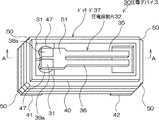
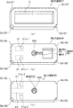
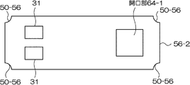
図1ないし図3は、本発明の圧電デバイスの第1の実施形態を示しており、図1はその概略斜視図、図2は図1のA−A線概略断面図、図3は図1の圧電デバイスのパッケージの底部を構成する各基板の図である。
これらの図において、圧電デバイス30は、圧電振動子を構成した例を示しており、圧電デバイス30は、図1および図2に示すように、パッケージ37内に圧電振動片32を収容している。パッケージ37は、例えば、後述するように、絶縁材料として、酸化アルミニウム質のセラミックグリーンシートを成形して形成される複数の基板を積層した後、焼結して形成されている。
1 to 3 show a first embodiment of a piezoelectric device according to the present invention. FIG. 1 is a schematic perspective view thereof, FIG. 2 is a schematic sectional view taken along line AA of FIG. 1, and FIG. It is a figure of each board | substrate which comprises the bottom part of the package of this piezoelectric device.
In these drawings, the
すなわち、この実施形態では、パッケージ37は、図3に示すような、第1の積層基板(以下、「基板」という)55と、第2の基板56と、第3の基板57とを積層して形成されており、このうち、第1の基板55と第2の基板56が、パッケージ37の底部を形成している。そして、パッケージ37は、図2および図3(a)に示すように、第3の基板57の内側の材料を除去することで、内部空間Sのスペースを形成している。この内部空間Sが圧電振動片32を収容するための収容空間である。そして、第2の基板56が絶縁性基体に相当し、この第2の基板56に圧電振動片32を接合している。
That is, in this embodiment, the
パッケージ37の内部空間S内の図において左端部付近において、内部空間Sに露出して内側底部を構成する絶縁性基体としての第2の基板56には、例えば、タングステンメタライズ上にニッケルメッキ及び金メッキで形成した電極部31,31が設けられている。
この電極部31,31は、図2に示す実装端子41、42と接続されており、外部から印加される駆動電圧を、圧電振動片32に供給するものである。具体的には、この実装端子41,42と電極部31,31は、パッケージ37外部をメタライズにより引き回したり、あるいは第1の基板55および第2の基板56の焼成前にタングステンメタライズ等を利用して形成した導電スルーホール31a等で接続することで形成できる。パッケージ37の四隅には、図1に示すように1/4円の形状でなるキャスタレーション50,50,50,50が形成されている。上述した電極部31,31は、基板上を水平に延長して、各キャスタレーション50の内周に形成した導電部でパッケージ37の厚み方向に引き回し、実装端子41,42と接続してもよい。
各電極部31,31の上には、導電性接着剤47が塗布されて、圧電振動片32の基部51が接合されている。この導電性接着剤47としては、例えば、合成樹脂などを利用したバインダー成分に、銀粒子などの導電粒子を混入したもので、機械的接合と電気的接続とを同時に行うことができるものである。
In the inner space S of the
The
A
パッケージ37は、図示の場合、内部空間Sを有する浅い箱状に形成され、平板状の蓋体40により気密に封止される構成であるが、これに限らず、例えば、第3の基板57を省略し、平板な第2の基板56の上に浅い箱状の図示しない蓋体を被せることで、蓋体内部に、圧電振動片を収容する空間を作るようにしたパッケージを使用してもよい。この場合においても、パッケージの底部はこの実施形態と同様の構造となる。
In the illustrated example, the
圧電振動片32は、例えば水晶で形成されており、水晶以外にもタンタル酸リチウム,ニオブ酸リチウム等の圧電材料を利用することができる。本実施形態の場合、圧電振動片32は、小型に形成して、必要な性能を得るために、図1に示す形状とされている。
すなわち、圧電振動片32は、パッケージ37側と固定される基部51と、この基部51を基端として、図において右方に向けて、二股に別れて平行に延びる一対の振動腕35,36を備えており、全体が音叉のような形状とされた、所謂、音叉型圧電振動片が利用されている。
The piezoelectric vibrating
That is, the piezoelectric vibrating
ここで、各振動腕35,36の主面には、好ましくは、それぞれ長さ方向に延びる長溝を形成し、この長溝内に励振電極を形成している(図示せず)。この長溝は、それぞれ振動腕35と、振動腕36の主面である表裏面に形成され、長溝内には励振電極がそれぞれ形成されており、各振動腕の長溝内に形成される励振電極は互いに分離された一対の電極とされている。これにより、励振電極に駆動電圧が印加されることによって、駆動時に、各振動腕の内部の電界効率を高めることができるようになっている。
Here, a long groove extending in the length direction is preferably formed on the main surface of each vibrating
また、圧電振動片32の基部51の端部の幅方向両端付近には、上述したように、パッケージ37の電極部31,31と接続するための電極部として、引出し電極38a,39aが形成されている。各引出し電極38a,39aは、基部51の外縁を回り込んで、圧電振動片32の基部51の表裏に設けられている。これらの各引出し電極38a,39aは上述した各励振電極と接続されており、例えば、水晶表面に、クロム(Cr)および金(Au)を順次メッキして形成することができる。また、振動腕35,36の少なくとも表面の先端領域には、この電極金属と同じ金属を利用して、電極形成の際に同時に周波数調整用の金属膜を形成してもよい。この金属膜に対して、図2のLB1に示すように、透明な蓋体40を透過させて、レーザ光のような加熱用の光ビームが照射され、これにより質量削減方式による周波数調整ができるようにされている。
In addition, as described above,
圧電振動片32は以上のように構成されており、引出し電極38a,39aから、図示しない励振電極に駆動電圧が印加されることにより、各振動腕35,36内で電界が適切に形成され、振動腕35,36の各先端部が互いに接近したり離間したりするように駆動されて、所定の周波数で振動する。
尚、圧電振動片としては、図示のような音叉型の圧電振動片に限らず、圧電材料を矩形にカットしたATカット振動片やコンベックスタイプの振動片等の種々の圧電振動片を使用することができる。
The piezoelectric vibrating
The piezoelectric vibrating piece is not limited to the tuning-fork type piezoelectric vibrating piece as shown in the figure, and various piezoelectric vibrating pieces such as an AT cut vibrating piece obtained by cutting a piezoelectric material into a rectangular shape or a convex type vibrating piece may be used. Can do.
パッケージ37の開放された上端には、蓋体40が接合されることにより、封止されている。
蓋体40は、好ましくは、上述した周波数調整を可能とするために、透明な材料で形成されており、例えば、パッケージ37側との熱膨張係数を近似させるために、硼珪酸ガラスなどにより形成されている。
A
The
さらに、この実施形態の圧電デバイス30では、パッケージ37の底部に、封止孔61を備えている。この封止孔61は、後述する脱ガス工程において、パッケージ37内の脱ガスを行うための孔である。
具体的には、封止孔61は、図2および図3に示されているように、第1の基板55に形成した外部に開く貫通孔62と、第2の基板56に形成された連絡部65を備えている。この連絡部65は、第1の基板55と第2の基板56とを図2のように重ねた状態において、第1の基板55の貫通孔62の周縁の一部と重なる箇所を基端として基板平面に沿って延びる細い幅の有底の溝63と、それより延長側に形成されて、パッケージ37の内部空間Sに開口している貫通部64とを備えている。
Further, in the
Specifically, as shown in FIG. 2 and FIG. 3, the sealing
ここで、貫通部64は、パッケージ37の内部空間Sに連絡していれば、溝63と同じ幅の開口とするなど、どのような構成でもよいが、この実施形態の場合、例えば、矩形の開口であり、比較的広い面積を備えている。貫通部64が広い面積とされていることで、圧電デバイス30に外部から衝撃が加えられた際に、圧電振動片32の各振動腕35,36の先端が下に振れた場合、パッケージ37の内側底部と衝突することを避けることができ、損傷を防止できる。
このような構成により、図2に示すように、封止孔61は、第2の基板56の底面が、第1の基板55の貫通孔62内で下向き段部66を形成しており、その貫通孔62の周縁の一部に、溝63と連通する隙間67を形成している。また、貫通孔62内の内周面には、封止材と接合性のよい金属被覆部68を備えている。そして、封止孔61の貫通孔62は、例えば、Au−Ge等の金属封止材71を充填して、気密に封止されている。
Here, the penetrating
With such a configuration, as shown in FIG. 2, the bottom surface of the
本実施形態の圧電デバイス30は以上のように形成されており、次にその製造方法の実施形態を説明する。
(圧電デバイスの製造方法)
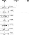
圧電デバイス30の製造方法の実施形態は、図4および図5のフローチャートを参照しながら説明する。
先ず、図1ないし図3で説明した圧電振動片32と蓋体40、パッケージ37は、図4の最上段に示すように、それぞれ別々に形成しておく。
(圧電振動片および蓋体の形成工程)
圧電振動片32については、例えば、水晶ウエハをエッチングして、既に説明した形状を形成するとともに、必要な励振電極を形成することで、従来と同様に製造することができるので、詳しい説明は省略する。電極形成後に、駆動電圧を印加して周波数を粗調整する。
蓋体40は、圧電振動片32とは別に形成される。この場合、蓋体40はガラスにより所定の形状と大きさに形成する。
The
(Piezoelectric device manufacturing method)
An embodiment of a method for manufacturing the
First, the piezoelectric vibrating
(Formation process of piezoelectric vibrating piece and lid)
The piezoelectric vibrating
The
(パッケージの形成工程)
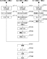
図3の第1の基板55、第2の基板56、第3の基板57は、図5に示すようにそれぞれ別々に成形した後で、積層される。
先ず、例えば、所定の溶液中にセラミックパウダを分散させ、バインダを添加して生成される混練物をシート状の長いテープ形状に成形し、これを所定の長さにカットして得た、所謂グリーンシート(図示せず)にする。
グリーンシートは、シート基板として上述した第1ないし第3の各基板55,56,57を形成するために共通して使用することができる。
(Package formation process)
The
First, for example, a so-called kneaded product obtained by dispersing ceramic powder in a predetermined solution, adding a binder, and forming the kneaded product into a sheet-like long tape shape, and cutting it into a predetermined length, so-called Use green sheets (not shown).
The green sheet can be used in common to form the first to
次に、各基板の成形と、電極パターン印刷、貫通孔の形成の工程を説明する。
図5のST11ないしST13は、図3の第3の基板57を成形する工程に対応している。尚、図3は理解の便宜のためひとつのパッケージ単位の大きさで表されているが、実際は基板の平面方向に縦横に同じものが連続する状態で成形がされる。
先ず、第3の基板57の形成例を説明する。
上記したグリーンシートをひとつのパッケージの大きさの単位に四隅に貫通孔を形成する。すなわち、図3(a)のキャスタレーション部50−57が打ち抜かれる(ST11)。
次に、グリーンシートの内側を矩形に打ち抜き、内部空間Sとなるキャビティを形成する(ST12)。
続いて、各キャスタレーション部50−57の内周面に導電ペーストとして、例えばタングステンメタライズなどを施し、導電部(図示せず)を形成する(ST13)。
Next, steps of forming each substrate, printing an electrode pattern, and forming a through hole will be described.
ST11 to ST13 in FIG. 5 correspond to the step of forming the
First, an example of forming the
Through holes are formed at the four corners in the unit of the size of the above-described green sheet. That is, the castellation part 50-57 of Fig.3 (a) is punched (ST11).
Next, the inside of the green sheet is punched into a rectangle to form a cavity that becomes the internal space S (ST12).
Subsequently, for example, tungsten metallization is applied to the inner peripheral surface of each castellation portion 50-57 as a conductive paste to form a conductive portion (not shown) (ST13).
次に、図3(b)の第2の基板56の形成例を説明する。
図3(b)は、第2の基板56の下面(図2における下を向いた面)を上にして、図示している。第2の基板56には、上記したグリーンシートをひとつのパッケージの大きさの単位に四隅に貫通孔を形成する。すなわち、図3(b)のキャスタレーション部50−56が打ち抜かれる(ST21)。
次に、グリーンシートの電極部31を形成する箇所などの必要箇所にスルーホール31a―1,31a―1を打ち抜く(ST22)。そして、このスルーホールにタングステンペーストを埋め込み、導電スルーホール31aなどを形成する(ST23)。なお、スルーホールは図示する箇所に限らず、必要な位置に必要な数だけ同様に形成する。
Next, an example of forming the
FIG. 3B illustrates the
Next, the through-
次に、抜き型等の所定の成形手段を用いて、貫通部64を打ち抜き、同時に溝63の部分を押し型等で加工する(ST24)。この抜き型と押し型は一体になったものを用いると加工精度が向上し、一度の工程で済むことから加工性に優れて好ましい。
続いて、キャスタレーション部50−56(ST25)、図3(b)では隠れている基板裏面(ST26)、および図3(b)の基板表面の電極部31,31に相当する箇所など(ST27)に順次、もしくは同時に導電パターンを形成するためにタングステンペーストなどでプリントを行う。また、第2の基板56の中央付近にタングステンペーストなどで、金属被覆部68の一部となる導電部68aを形成する。
また、上記の方法とは別に、溝63の部分を形成するようにしてもよい。すなわち、貫通部64の部分は材料を打ち抜くこととして、溝63に対応する部分には、基板の焼成温度付近の温度で溶融あるいは焼失するような溝形成材(図示せず)を配置しておく。例えば、細い紐状の合成あるいは天然繊維、リボン状、あるいは棒状の合成樹脂材料などでなる溝形成材を、溝63と対応する箇所に配置しておく。その後、上から加圧するか、あるいは、単に配置しておき、後述する積層の工程で、焼成前の可塑性のある状態の基板材料に、加圧により埋め込まれるようにしておく。また、第2の基板56の上面に、ペースト状などの溝形成材を印刷で配置してもよい。
これにより、後述するように、第1ないし第3の基板を積層後、焼結する際に、溝形成材が熱により溶融もしくは焼失し、溝63として、気体のリークに十分な細い溝が形成されることになる。なお、溝形成材は、使用する基板材料の焼結温度、例えば、本実施形態では、1200度ないし1500度(摂氏)程度で、溶融もしくは焼失するものが選択される。
Next, using a predetermined forming means such as a punching die, the penetrating
Subsequently, the castellation part 50-56 (ST25), the substrate back surface (ST26) hidden in FIG. 3B, the portions corresponding to the
In addition to the above method, the
As a result, as will be described later, when the first to third substrates are laminated and then sintered, the groove forming material is melted or burned by heat, and a groove sufficiently narrow to leak gas is formed as the
次に、図3(c)の第1の基板55の形成例を説明する。
図3(c)は、第1の基板55の上面側を示している。先ず、第1の基板55に、上記したグリーンシートをひとつのパッケージの大きさの単位に四隅に貫通孔を形成する。すなわち、図3(c)のキャスタレーション部50−55が打ち抜かれる(ST31)。
次に、第1の基板55に相当するグリーンシートのほぼ中央付近に貫通孔62を打ち抜く(ST32)。続いて、キャスタレーション部50−55(ST33)、図3(c)では隠れている基板裏面(ST34)、すなわち、図2で説明した実装端子41,41となる部分や、スルーホール31aの一部を構成するスルーホール31a−2,31a−2、金属被覆部68の一部となる導電部68bなどに順次、もしくは同時に導電パターンを形成するためにタングステンペーストなどでプリントを行う。
なお、実装端子となる部分は、図示の位置に限らず、第1の基板55の四隅に形成し、必要な配線を行ってもよい。
Next, an example of forming the
FIG. 3C shows the upper surface side of the
Next, the through-
Note that the portions to be mounting terminals are not limited to the illustrated positions, and may be formed at the four corners of the
次いで、成形後の第1の基板55の上に成形後の第2の基板56を、第2の基板56の上に成形後の第3の基板57を重ねることで積層するが、この際には、必要により重合面に結合剤を塗布しておく(ST41)。
次いで、各基板を積層した状態のグリーンシートの縦横の切断線に沿って、例えば、パッケージ4個分単位となるように、スナップカットし(ST42)。続いて、図1のキャスタレーション50を交叉位置とする個々のパッケージ単位の大きさとなる縦横の切断線に沿って切断する(ST43)。
その後、1200度ないし1500度(摂氏)で焼結する(ST44)。焼結後には、タングステンメタライズの上にニッケルメッキおよび金メッキを順次施して、電極や端子および導電パターンなどを形成して、図1や図2に示すようなパッケージ37を完成する。なお、パッケージ37の上端には、低融点ガラスなどの封止材58(図2参照)を塗布しておく。
Next, the
Next, snap cutting is performed along the vertical and horizontal cutting lines of the green sheets in a state where the respective substrates are stacked, for example, so as to be a unit of four packages (ST42). Subsequently, cutting is performed along vertical and horizontal cutting lines that are the size of each package unit with the
Thereafter, sintering is performed at 1200 to 1500 degrees (Celsius) (ST44). After sintering, nickel plating and gold plating are sequentially performed on the tungsten metallization to form electrodes, terminals, conductive patterns, and the like, and a
(圧電振動片の接合工程)
次に、図4において、図2に示すように、圧電振動片32をパッケージ37の電極部31の上に接合する(ST51)。すなわち、図1および図2で説明したように、パッケージ37の電極部31上に導電性接着剤47を塗布して、その上に圧電振動片32の基部51の引き出し電極38a,39aの個所を載置し、導電性接着剤47,47を硬化させることにより、電極部31と圧電振動片32とが電気的、機械的に接合される。このようにして、圧電振動片32は、絶縁基体である第2の基板56に対して、片持ち式に接合される。
(Piezoelectric vibrating piece joining process)
Next, in FIG. 4, as shown in FIG. 2, the piezoelectric vibrating
(蓋封止工程)
さらに、パッケージ37と蓋体40とを真空雰囲気中で、接合すること蓋封止を行う(ST52)。
ここで、重要なのは、この段階では、図2に示すように、貫通孔62がパッケージ37の内部と隙間67を介して外部と連通させている点である。
具体的には、図2のパッケージ37の内部空間Sは、第2の基板56に形成した貫通部65から、細い幅の連絡部64を通り,第1の基板55の貫通孔62とつながっており、外部と通気できるようにされている。
(Lid sealing process)
Further, the
Here, what is important is that, at this stage, as shown in FIG. 2, the through-
Specifically, the internal space S of the
(脱ガス工程)
この状態で、真空チャンバーなどに収容し、加熱することでアニール処理を行う(ST53)。この処理すなわち、脱ガスの工程では、パッケージ37内部のガスは第2の基板56の貫通部64、細い幅の連絡部65、第1の基板55の貫通孔62の隙間67をそれぞれ通過して、パッケージ37の外部に排出される。
(孔封止工程)
次に、図2の封止孔61を孔封止する(ST54)。
具体的には、第1の基板55の外部に開いた貫通孔62を、例えば、図2の上下を逆にして、その段部66を上に向ける。この段部66に、例えば、球形のAu−Ge等でなる金属封止材、すなわち、リジットな状態の金属封止材を載せる。
次いで、図2に示されているように、この金属封止材にレーザ等の加熱ビームLB2を照射して溶融させて、封止孔61内に充填する。この場合に、加熱ビームは金属封止材の溶融の際に第2の基板56の段部66に当たり、貫通することができないから、加熱ビームLB2がパッケージ37内部に侵入することがなく、圧電振動片32に照射されるおそれがない。このため、圧電振動片32の周波数をシフトさせることがない。
これにより、安全かつ確実に封止孔61を気密封止することができる。
(Degassing process)
In this state, the substrate is housed in a vacuum chamber or the like and heated for annealing (ST53). In this process, that is, the degassing step, the gas inside the
(Hole sealing process)
Next, the sealing
Specifically, for example, the through
Next, as shown in FIG. 2, the metal sealing material is irradiated with a heating beam LB2 such as a laser to be melted and filled in the sealing
Thereby, the sealing
(周波数調整)
次に、図2に示されているように、透明な蓋体40を介して、外部から加熱用の光ビーム、例えば、レーザ光LB1を、圧電振動片32の先端付近の電極もしくは金属被覆部に照射して、質量削減方式による周波数調整を行う(ST56)。
最後に、必要な検査を行い(ST57)、圧電デバイス30が完成する(ST58)。
(Frequency adjustment)
Next, as shown in FIG. 2, a heating light beam, for example, a laser beam LB <b> 1 is applied from the outside via a
Finally, necessary inspection is performed (ST57), and the
以上述べたように、この実施形態に係る製造方法では、パッケージの形成の際に、第1の基板55に封止孔61となる貫通孔を、第2の基板56に細い幅の連絡部65を簡単に製造することができ、孔封止工程で圧電振動片32を損傷しない構造を容易に形成することができる。
As described above, in the manufacturing method according to this embodiment, when the package is formed, the
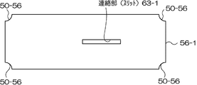
図6ないし図8は、圧電デバイスの第2の実施形態を示しており、図6は圧電デバイスの概略断面図、図7はそのパッケージの底部を形成するための第3の基板の概略平面図、図8はそのパッケージの底部を形成するための第2の基板の概略平面図である。
これらの図において、第1の実施形態と共通する構成には同一の符号を付して、重複する説明は省略し、以下、相違点を中心に説明する。
6 to 8 show a second embodiment of the piezoelectric device, FIG. 6 is a schematic sectional view of the piezoelectric device, and FIG. 7 is a schematic plan view of a third substrate for forming the bottom of the package. FIG. 8 is a schematic plan view of a second substrate for forming the bottom of the package.
In these drawings, the same components as those in the first embodiment are denoted by the same reference numerals, and redundant description is omitted. Hereinafter, differences will be mainly described.
圧電デバイス80は、第1の実施形態の圧電デバイス30と比較すると、パッケージ底部の構造だけが相違している。したがって、その製造方法の実施形態においても、底部の構造の相違に対応した箇所だけが異なり、その他の点では同じである。
パッケージ37−1においては、第1の実施形態と異なり、図6に示されているように、第1の基板55,第2の基板56−1、第3の基板56−2、第4の基板57を積層することにより形成されている。そして、パッケージ底部は、第1の実施形態と異なり、第1の基板55,第2の基板56−1、第3の基板56−2の3層の基板を積層して形成されている。これら積層基板のうち、第1の基板55の構成は第1の実施形態の第1の基板と同じで、第4の基板57は、第1の実施形態における第3の基板57と全く同じ構成である。相違する点は、いわば、第1の実施形態における第2の基板56が、この実施形態では、第2の基板56−1と、第3の基板56−2に分かれた構造となっている点である。
The
In the package 37-1, unlike the first embodiment, as shown in FIG. 6, the
第1の基板55の上に積層される第2の基板56―1は、図8に示されているように、細い幅の連絡部としてのスリット63−1を備えており、このスリット63−1は、第2の基板56−1を貫通した構成とされている。
そして、第2の基板56−1の上に積層される第3の基板56−2は、図7に示すように、貫通した矩形の開口部64−1を備えている。
図6に示されているように、スリット63−1の基端部は、第1の基板55の貫通孔62の周縁付近と重なる位置である。このため、封止孔61は、第1の隙間67を備えている。また、スリット63−1の延長端は、開口部64−1の外縁部と重なる位置に達している。このため、封止孔61は、パッケージ37の内側で第2の隙間67−1を備えている。
As shown in FIG. 8, the second substrate 56-1 laminated on the
And the 3rd board | substrate 56-2 laminated | stacked on the 2nd board | substrate 56-1 is provided with the rectangular opening part 64-1, which penetrated, as shown in FIG.
As shown in FIG. 6, the base end portion of the slit 63-1 is a position overlapping the vicinity of the peripheral edge of the through
このように、圧電デバイス80では、パッケージ37―1の内部空間Sは第3の基板56−2の開口部64−1から、第2の基板56−1の細い幅の連絡部63−1を通り、第1の基板55の貫通孔62とつながっており、外部と通気できるようにされている。これにより、製造工程における脱ガスの工程(図4、ST53参照)では、パッケージ内部のガスは第3の基板56−2の開口部64−1、第2の基板56−1の細い幅の連絡部63−1、第1の基板55の貫通孔62をそれぞれ通過して、パッケージ37の外部に排出される。
また、第1の基板55の外部に開いた貫通孔62に金属封止材を充填して封止孔61を封止する際に、この貫通孔62に臨ませてリジットな金属封止材を配置した状態においては、この金属封止材にレーザ等の加熱ビームLB2を照射して溶融させる場合に、加熱ビームは金属封止材の溶融の際に第2の基板56−1を貫通することができないから、加熱ビームがパッケージ37内部に侵入することがなく、圧電振動片32に照射されるおそれがない。このため、周波数をシフトさせることがない。
As described above, in the
Further, when the sealing
しかも、第1の基板55の貫通孔62と第3の基板56−2の開口部64−1を介して、パッケージ37の内部空間Sとをつなぐ部分は、細い幅の連絡部63−1とされることにより、大きなスリットや開口とする場合に比べて、パッケージ底部の強度を十分に確保して、通気構造を実現できる。
さらに、この実施形態では、第1の実施形態と比べて、多い数の積層基板を利用してパッケージの底部を形成していることからも、封止孔61を形成することにより剛性の低下のおそれがある底部の構造をより強化することができる。
また、第2の実施形態の圧電デバイス80は、パッケージの製造に際して、第1の実施形態よりも多い数の基板を形成することを除き、第1の実施形態と同様の方法で製造することができ、各積層基板の製造方法も上述した手法と同じである。
In addition, the portion connecting the internal space S of the
Furthermore, in this embodiment, compared to the first embodiment, since the bottom of the package is formed using a larger number of laminated substrates, the formation of the sealing
Further, the
本発明は上述の実施形態に限定されない。各実施形態の各構成はこれらを適宜組み合わせたり、省略し、図示しない他の構成と組み合わせることができる。
また、この発明は、パッケージや箱状の蓋体に被われるようにして、内部に圧電振動片もしくは圧電振動片とICなどの電子部品を収容するものであれば、圧電振動子、圧電発振器等の名称にかかわらず、全ての圧電デバイスに適用することができる。
The present invention is not limited to the above-described embodiment. Each configuration of each embodiment can be appropriately combined or omitted, and can be combined with other configurations not shown.
In addition, the present invention provides a piezoelectric vibrator, a piezoelectric oscillator, or the like as long as it is covered with a package or a box-shaped lid and accommodates a piezoelectric vibrating piece or a piezoelectric vibrating piece and an electronic component such as an IC. Regardless of the name, it can be applied to all piezoelectric devices.
30,80・・・圧電デバイス、32・・・圧電振動片、35,36・・・振動腕、31・・・電極部、37・・・パッケージ、47・・・導電性接着剤、55・・・第1の基板、56・・・第2の基板、57・・・第3の基板。
30, 80 ... piezoelectric device, 32 ... piezoelectric vibrating piece, 35,36 ... vibrating arm, 31 ... electrode part, 37 ... package, 47 ... conductive adhesive, 55. ..
Claims (8)
前記パッケージが複数層の絶縁基板を積層した底部を有しており、
最も外側に位置する第1の基板には、外部に開いた貫通孔が形成されていて、
前記第1の基板に重ねられた第2の基板には、前記貫通孔の一部と重なる箇所を基端として基板平面に沿って延びる細い幅の連絡部が形成されており、
前記連絡部は、基端側が前記貫通孔と連通した有底の溝であり、延長端側が前記パッケージ内部に開口している貫通部を備えている
ことを特徴とする、圧電デバイス。 A piezoelectric device that houses a piezoelectric vibrating piece in a package and hermetically seals the package,
The package has a bottom portion on which a plurality of insulating substrates are stacked;
The first substrate located on the outermost side has a through-hole opened to the outside,
The second substrate overlaid on the first substrate is formed with a narrow-width connecting portion extending along the substrate plane with a portion overlapping with a part of the through hole as a base end,
The piezoelectric device according to claim 1, wherein the connecting portion includes a bottomed groove that communicates with the through hole on a base end side, and a through portion that opens to the inside of the package on an extended end side.
前記パッケージが複数層の絶縁基板を積層した底部を有しており、
前記底部を構成する複数層の前記絶縁基板として、少なくとも第1ないし第3の3枚の基板を有しており、
最も外側に位置する第1の基板には、外部に開いた貫通孔が形成されていて、
前記第1の基板に重ねられた第2の基板には、前記貫通孔の一部と重なる箇所を基端として基板平面に沿って延びる細い幅の連絡部が形成されており、
前記第2の基板に重ねられる第3の基板には、前記貫通孔と重ならない位置に前記パッケージ内部に開口する開口部が形成され、
かつ前記連絡部は、基端側が前記貫通孔と連通し、延長端側が前記開口部と連通する構成とした
ことを特徴とする、圧電デバイス。 A piezoelectric device that houses a piezoelectric vibrating piece in a package and hermetically seals the package,
The package has a bottom portion on which a plurality of insulating substrates are stacked;
As the insulating substrate of the plurality of layers constituting the bottom portion, at least first to third substrates are included,
The first substrate located on the outermost side has a through-hole opened to the outside,
The second substrate overlaid on the first substrate is formed with a narrow-width connecting portion extending along the substrate plane with a portion overlapping with a part of the through hole as a base end,
In the third substrate overlaid on the second substrate, an opening that opens inside the package is formed at a position that does not overlap the through hole,
The connecting portion has a configuration in which a base end side communicates with the through hole and an extension end side communicates with the opening.
前記パッケージと、前記圧電振動片と、前記蓋体とを別々に形成するための個別の形成工程と、
前記パッケージを構成する絶縁性基体に対して、前記圧電振動片を接合する工程と、
前記パッケージを前記蓋体により気密に封止する蓋封止工程と、
前記パッケージの外部から前記圧電振動片に形成されている金属膜に加熱用光ビームを照射する周波数調整工程と
前記パッケージに設けた貫通孔を利用して、加熱下で脱ガスした後で、この貫通孔を封止する孔封止工程と
を有しており、
前記パッケージの形成工程では、複数の絶縁性基板を成形後、積層し焼結するようにされており、
前記パッケージの底部を形成するための最も外側に位置する第1の基板には、前記成形の際に貫通孔が形成され、
前記第1の基板に重ねられる第2の基板の前記成形時には、前記貫通孔の一部と重なる箇所を基端として、基板平面に沿って延びる細い幅の連絡部が形成されるとともに、この連絡部は、基端側が前記貫通孔と連通される有底の溝とされ、延長端側が前記パッケージ内部に開口する貫通部となるようにされる
ことを特徴とする、圧電デバイスの製造方法。 A method of manufacturing a piezoelectric device in which a piezoelectric vibrating piece is accommodated in a package and hermetically sealed,
An individual forming step for separately forming the package, the piezoelectric vibrating piece, and the lid;
Bonding the piezoelectric vibrating piece to an insulating substrate constituting the package;
A lid sealing step for hermetically sealing the package with the lid;
After degassing under heating by using a frequency adjustment step of irradiating a metal film formed on the piezoelectric vibrating piece from the outside of the package with a light beam for heating and a through hole provided in the package, A hole sealing step for sealing the through hole,
In the process of forming the package, a plurality of insulating substrates are formed, stacked and sintered,
The first substrate located on the outermost side for forming the bottom of the package has a through hole formed during the molding,
At the time of forming the second substrate overlaid on the first substrate, a narrow-width connecting portion extending along the substrate plane is formed starting from a portion that overlaps a part of the through hole. The manufacturing method of the piezoelectric device according to claim 1, wherein the part has a bottomed groove that communicates with the through hole at a base end side, and a through part that opens into the package at an extended end side.
前記パッケージと、前記圧電振動片と、前記蓋体とを別々に形成するための個別の形成工程と、
前記パッケージを構成する絶縁性基体に対して、前記圧電振動片を接合する工程と、
前記パッケージを前記蓋体により気密に封止する蓋封止工程と、
前記パッケージの外部から前記圧電振動片に形成されている金属膜に加熱用光ビームを照射する周波数調整工程と
前記パッケージに設けた貫通孔を利用して、加熱下で脱ガスした後で、この貫通孔を封止する孔封止工程と
を有しており、
前記パッケージの形成工程では、複数の絶縁性基板を成形後、積層し焼結するようにされており、
前記パッケージの底部を形成するための最も外側に位置する第1の基板には、前記成形の際に貫通孔が形成され、
前記第1の基板に重ねられる第2の基板の前記成形時には、前記貫通孔の一部と重なる箇所を基端として基板平面に沿って延びる細い幅の連絡部が形成され、
前記第2の基板に重ねられる第3の基板には、前記貫通孔と重ならない位置に前記パッケージ内部に開口する開口部が形成されるとともに、前記連絡部は、基端側が前記貫通孔と連通し、延長端側が前記開口部と連通するようにされる
ことを特徴とする、圧電デバイスの製造方法。 A method of manufacturing a piezoelectric device in which a piezoelectric vibrating piece is accommodated in a package and hermetically sealed,
An individual forming step for separately forming the package, the piezoelectric vibrating piece, and the lid;
Bonding the piezoelectric vibrating piece to an insulating substrate constituting the package;
A lid sealing step for hermetically sealing the package with the lid;
After degassing under heating by using a frequency adjustment step of irradiating a metal film formed on the piezoelectric vibrating piece from the outside of the package with a light beam for heating and a through hole provided in the package, A hole sealing step for sealing the through hole,
In the process of forming the package, a plurality of insulating substrates are formed, stacked and sintered,
The first substrate located on the outermost side for forming the bottom of the package has a through hole formed during the molding,
During the molding of the second substrate overlaid on the first substrate, a narrow-width connecting portion extending along the substrate plane with a portion overlapping with a part of the through hole as a base end is formed,
The third substrate overlaid on the second substrate has an opening that opens into the package at a position that does not overlap with the through-hole, and the communication portion has a proximal end communicating with the through-hole. And the extended end side is made to communicate with the said opening part. The manufacturing method of the piezoelectric device characterized by the above-mentioned.
複数層の絶縁基板を積層した底部を有しており、
最も外側に位置する第1の基板には、外部に開いた貫通孔が形成されていて、
前記第1の基板に重ねられた第2の基板には、前記貫通孔の一部と重なる箇所を基端として基板平面に沿って延びる細い幅の連絡部が形成されており、
前記連絡部は、基端側が前記貫通孔と連通した有底の溝であり、延長端側が前記内部空間に開口している貫通部を備えている
ことを特徴とする、パッケージ。 A package for accommodating an electronic component in an internal space and sealing hermetically,
It has a bottom where multiple layers of insulating substrates are stacked,
The first substrate located on the outermost side has a through-hole opened to the outside,
The second substrate overlaid on the first substrate is formed with a narrow-width connecting portion extending along the substrate plane with a portion overlapping with a part of the through hole as a base end,
The package is characterized in that the connecting portion includes a bottomed groove that communicates with the through hole on the base end side, and a through portion that opens to the internal space on the extended end side.
複数層の絶縁基板を積層した底部を有しており、
前記底部を構成する複数層の前記絶縁基板として、少なくとも第1ないし第3の3枚の基板を有しており、
最も外側に位置する第1の基板には、外部に開いた貫通孔が形成されていて、
前記第1の基板に重ねられた第2の基板には、前記貫通孔の一部と重なる箇所を基端として基板平面に沿って延びる細い幅の連絡部が形成されており、
前記第2の基板に重ねられる第3の基板には、前記貫通孔と重ならない位置に前記パッケージ内部に開口する開口部が形成され、
かつ前記連絡部は、基端側が前記貫通孔と連通し、延長端側が前記開口部と連通する構成とした
ことを特徴とする、パッケージ。 A package for accommodating an electronic component in an internal space and sealing hermetically,
It has a bottom where multiple layers of insulating substrates are stacked,
As the insulating substrate of the plurality of layers constituting the bottom portion, at least first to third substrates are included,
The first substrate located on the outermost side has a through-hole opened to the outside,
The second substrate overlaid on the first substrate is formed with a narrow-width connecting portion extending along the substrate plane with a portion overlapping with a part of the through hole as a base end,
In the third substrate overlaid on the second substrate, an opening that opens inside the package is formed at a position that does not overlap the through hole,
And the said connection part was set as the structure which the base end side connected with the said through-hole, and the extended end side connected with the said opening part. The package characterized by the above-mentioned.
Priority Applications (1)
| Application Number | Priority Date | Filing Date | Title |
|---|---|---|---|
| JP2004109165A JP2005295322A (en) | 2004-04-01 | 2004-04-01 | Package, piezoelectric device and manufacturing method thereof |
Applications Claiming Priority (1)
| Application Number | Priority Date | Filing Date | Title |
|---|---|---|---|
| JP2004109165A JP2005295322A (en) | 2004-04-01 | 2004-04-01 | Package, piezoelectric device and manufacturing method thereof |
Publications (1)
| Publication Number | Publication Date |
|---|---|
| JP2005295322A true JP2005295322A (en) | 2005-10-20 |
Family
ID=35327747
Family Applications (1)
| Application Number | Title | Priority Date | Filing Date |
|---|---|---|---|
| JP2004109165A Pending JP2005295322A (en) | 2004-04-01 | 2004-04-01 | Package, piezoelectric device and manufacturing method thereof |
Country Status (1)
| Country | Link |
|---|---|
| JP (1) | JP2005295322A (en) |
Cited By (3)
| Publication number | Priority date | Publication date | Assignee | Title |
|---|---|---|---|---|
| JP2007184859A (en) * | 2006-01-10 | 2007-07-19 | Epson Toyocom Corp | Hermetic sealing structure, piezoelectric device and manufacturing method thereof |
| JP2010087930A (en) * | 2008-09-30 | 2010-04-15 | Citizen Finetech Miyota Co Ltd | Piezoelectric device |
| JP2017229017A (en) * | 2016-06-24 | 2017-12-28 | セイコーエプソン株式会社 | Vibration device, method of manufacturing vibration device, electronic device, and movable body |
-
2004
- 2004-04-01 JP JP2004109165A patent/JP2005295322A/en active Pending
Cited By (3)
| Publication number | Priority date | Publication date | Assignee | Title |
|---|---|---|---|---|
| JP2007184859A (en) * | 2006-01-10 | 2007-07-19 | Epson Toyocom Corp | Hermetic sealing structure, piezoelectric device and manufacturing method thereof |
| JP2010087930A (en) * | 2008-09-30 | 2010-04-15 | Citizen Finetech Miyota Co Ltd | Piezoelectric device |
| JP2017229017A (en) * | 2016-06-24 | 2017-12-28 | セイコーエプソン株式会社 | Vibration device, method of manufacturing vibration device, electronic device, and movable body |
Similar Documents
| Publication | Publication Date | Title |
|---|---|---|
| US6541897B2 (en) | Piezoelectric device and package thereof | |
| JP2008236741A (en) | Package type piezoelectric vibrator and manufacturing method of package type piezoelectric vibrator | |
| US8499443B2 (en) | Method of manufacturing a piezoelectric vibrator | |
| JP5550373B2 (en) | Package manufacturing method | |
| JP2005278069A (en) | Piezoelectric vibrating piece and piezoelectric device using the same | |
| JP4038819B2 (en) | Surface-mount type piezoelectric device and its container, mobile phone device using surface-mount type piezoelectric device, and electronic equipment using surface-mount type piezoelectric device | |
| JP4341268B2 (en) | Package for piezoelectric device, piezoelectric device, mobile phone device using piezoelectric device, and electronic equipment using piezoelectric device | |
| JP2005295322A (en) | Package, piezoelectric device and manufacturing method thereof | |
| JP2005109886A (en) | Piezoelectric device, manufacturing method thereof, mobile phone device using piezoelectric device, and electronic apparatus using piezoelectric device | |
| JP4292575B2 (en) | Piezoelectric device and method of manufacturing lid | |
| JP2006074567A (en) | Piezoelectric device | |
| JP2003069368A (en) | Method for joining piezoelectric device and piezoelectric vibrating reed, mobile phone device using piezoelectric device, and electronic device using piezoelectric device | |
| JP2006033458A (en) | Package, piezoelectric device and manufacturing method thereof | |
| JP4144036B2 (en) | Electronic component package and piezoelectric vibration device using the electronic component package | |
| JP2004289478A (en) | Bonding structure of piezoelectric vibrating reed, piezoelectric device and manufacturing method thereof, mobile phone device using piezoelectric device, and electronic device using piezoelectric device | |
| JP4114149B2 (en) | Piezoelectric device, manufacturing method thereof, mobile phone device using piezoelectric device, and electronic apparatus using piezoelectric device | |
| JP2005051408A (en) | Piezoelectric device, manufacturing method thereof, mobile phone device using the piezoelectric device, and electronic equipment using the piezoelectric device | |
| JP2005065189A (en) | Piezoelectric device, manufacturing method thereof, mobile phone device using piezoelectric device, and electronic apparatus using piezoelectric device | |
| JP2005184229A (en) | Piezoelectric device, manufacturing method thereof, package for piezoelectric device, mobile phone device using piezoelectric device, and electronic apparatus using piezoelectric device | |
| JP2009284125A (en) | Package for crystal oscillator, and crystal oscillator | |
| JP2006157504A (en) | Method for manufacturing piezoelectric device and glass lid | |
| JP4472445B2 (en) | Method for manufacturing piezoelectric oscillator | |
| JP2006074568A (en) | Method for manufacturing piezoelectric device | |
| JP2005094461A (en) | Piezoelectric device, manufacturing method thereof, mobile phone device using piezoelectric device, and electronic apparatus using piezoelectric device | |
| JP2005244500A (en) | Piezoelectric device, manufacturing method thereof, package for piezoelectric device, mobile phone device using piezoelectric device, and electronic apparatus using piezoelectric device |
Legal Events
| Date | Code | Title | Description |
|---|---|---|---|
| A621 | Written request for application examination |
Free format text: JAPANESE INTERMEDIATE CODE: A621 Effective date: 20051209 |
|
| A977 | Report on retrieval |
Free format text: JAPANESE INTERMEDIATE CODE: A971007 Effective date: 20080828 |
|
| A131 | Notification of reasons for refusal |
Free format text: JAPANESE INTERMEDIATE CODE: A131 Effective date: 20080917 |
|
| A521 | Request for written amendment filed |
Free format text: JAPANESE INTERMEDIATE CODE: A523 Effective date: 20081117 |
|
| A02 | Decision of refusal |
Free format text: JAPANESE INTERMEDIATE CODE: A02 Effective date: 20090402 |