JP2005295300A - Dielectric filter - Google Patents
Dielectric filter Download PDFInfo
- Publication number
- JP2005295300A JP2005295300A JP2004108877A JP2004108877A JP2005295300A JP 2005295300 A JP2005295300 A JP 2005295300A JP 2004108877 A JP2004108877 A JP 2004108877A JP 2004108877 A JP2004108877 A JP 2004108877A JP 2005295300 A JP2005295300 A JP 2005295300A
- Authority
- JP
- Japan
- Prior art keywords
- dielectric
- filter
- circuit
- parallel circuit
- dielectric filter
- Prior art date
- Legal status (The legal status is an assumption and is not a legal conclusion. Google has not performed a legal analysis and makes no representation as to the accuracy of the status listed.)
- Pending
Links
Images


Landscapes
- Control Of Motors That Do Not Use Commutators (AREA)
- Filters And Equalizers (AREA)
Abstract
【課題】積層数を減らした小型の誘電体フィルタを提供することにある。
【解決手段】複数個の誘電体層1a〜1iを積層してなる積層体1の内部に、LC並列回路Fpの一端側にLC直列回路Fsを接続したフィルタ素子を配設してなる誘電体フィルタにおいて、LC並列回路Fpの容量成分C1とLC直列回路Fsの容量成分C2とが共通の誘電体層1f内に形成されている
【選択図】図2A compact dielectric filter with a reduced number of layers is provided.
A dielectric body in which a filter element in which an LC series circuit Fs is connected to one end of an LC parallel circuit Fp is disposed inside a multilayer body 1 formed by laminating a plurality of dielectric layers 1a to 1i. in the filter, LC BACKGROUND oF capacitance component C 2 and are formed on a common dielectric layer 1f of the capacitance component C 1 and the LC series circuit Fs parallel circuit Fp 2
Description
本発明は、内部にLC共振回路を有した積層型の誘電体フィルタに関するものである。 The present invention relates to a multilayer dielectric filter having an LC resonance circuit therein.
従来より、携帯電話等の高周波通信機器にLC共振回路を内部に有した誘電体フィルタが用いられている。 Conventionally, a dielectric filter having an LC resonance circuit in a high-frequency communication device such as a mobile phone has been used.
かかる従来の誘電体フィルタは、例えば、複数個の誘電体層を積層してなる積層体の内部に、LC並列回路の一端側にLC直列回路を接続したフィルタ素子を配設した構成のものが知られている(例えば、特許文献1参照。)。 Such a conventional dielectric filter has, for example, a structure in which a filter element in which an LC series circuit is connected to one end side of an LC parallel circuit is disposed in a laminate formed by laminating a plurality of dielectric layers. It is known (for example, refer to Patent Document 1).
上記誘電体フィルタの周波数特性は、LC並列回路の共振によりインピーダンスが無限大となり信号の通過が阻止されることによって形成される減衰極と、LC直列回路が共振によりインピーダンスが無限小となり信号がグランド電位に流れることによって形成される減衰極とを有しており、このような2つの減衰極を形成することによって広い阻止域を形成するようにしている。
しかしながら、上述した従来の誘電体フィルタにおいては、LC並列回路及びLC直列回路を構成するそれぞれの静電容量成分を異なる誘電体層に形成するようにしていることから、誘電体層の積層数が多くなってしまい、全体構造の小型化を図ることが困難であるという欠点を有していた。 However, in the above-described conventional dielectric filter, the capacitance components constituting the LC parallel circuit and the LC series circuit are formed in different dielectric layers, so the number of dielectric layers stacked is small. As a result, it has been disadvantageous in that it is difficult to reduce the size of the entire structure.
本発明は上記欠点に鑑み案出されたもので、その目的は、誘電体層の積層数を少なくすることにより全体構造の小型化を図ることができる誘電体フィルタを提供することにある。 The present invention has been devised in view of the above-described drawbacks, and an object of the present invention is to provide a dielectric filter capable of reducing the overall structure by reducing the number of laminated dielectric layers.
本発明の誘電体フィルタは、複数個の誘電体層を積層してなる積層体の内部に、LC並列回路の一端側にLC直列回路を接続したフィルタ素子を配設してなる誘電体フィルタにおいて、前記LC並列回路の容量成分C1と前記LC直列回路の容量成分C2とが共通の誘電体層内に形成されていることを特徴とするものである。 The dielectric filter of the present invention is a dielectric filter in which a filter element in which an LC series circuit is connected to one end side of an LC parallel circuit is disposed in a laminate formed by laminating a plurality of dielectric layers. and it is characterized in that the capacitance component C 2 of the LC series circuit and capacitance component C 1 of the LC parallel circuit is formed on a common dielectric layer.
また本発明の誘電体フィルタは、前記LC並列回路の誘導成分L1が、前記LC直列回路の前記容量電極と誘電体層を介して対向するように配設された周回パターンによって形成されていることを特徴とするものである。 The dielectric filter of the present invention, inductive component L 1 of the LC parallel circuit is formed by a circumferential pattern which is disposed so as to face each other through the capacitor electrode and the dielectric layer of the LC series circuit It is characterized by this.
更に本発明の誘電体フィルタは、前記LC並列回路の他端側に入力端子が、一端側に出力端子が接続されており、該出力端子と前記LC並列回路の一端部との間に、一端側をグランド端子に接続した前記LC直列回路の他端側を接続するようにしたことを特徴とするものである。 Furthermore, the dielectric filter of the present invention has an input terminal connected to the other end side of the LC parallel circuit and an output terminal connected to one end side, and one end between the output terminal and one end of the LC parallel circuit. The other end side of the LC series circuit whose side is connected to the ground terminal is connected.
本発明の誘電体フィルタによれば、LC並列回路の容量成分C1と、LC直列回路の容量成分C2とを共通の誘電体層内に形成するようにしたことから、誘電体層の積層数が少なくなり、全体構造の小型化を図ることができるようになる。またこの場合、2つの減衰極を形成するそれぞれのLC回路(LC並列回路及びLC直列回路)の容量成分が、共通の誘電体層内に形成されているため、誘電体層の厚み等がばらついても、この2つのLC回路の容量成分比は変わらなくなっており、2つの減衰極の間隔をほとんど変化させることなく阻止域全体の減衰量を安定させることができる利点もある。 According to the dielectric filter of the present invention, the capacitance component C 1 of the LC parallel circuit, since it has to form a capacitance component C 2 of the LC series circuits on a common dielectric layer, a stack of dielectric layers The number is reduced, and the overall structure can be reduced in size. In this case, since the capacitance components of the respective LC circuits (LC parallel circuit and LC series circuit) forming the two attenuation poles are formed in the common dielectric layer, the thickness of the dielectric layer varies. However, the capacitance component ratio of the two LC circuits does not change, and there is also an advantage that the attenuation amount of the entire stop band can be stabilized without substantially changing the interval between the two attenuation poles.
更に本発明の誘電体フィルタによれば、LC並列回路の誘導成分L1を、LC直列回路の容量電極と誘電体層を介して対向するように配設させておくことにより、LC並列回路の誘導成分L1である周回パターンとLC直列回路の容量電極との間にも容量成分が形成されることとなり、これによって良好な周波数特性が得られ易くなる。しかも、1つの容量電極で2つの容量成分が形成されるようになっているため、誘電体フィルタの構成も簡素化される。 Furthermore, according to the dielectric filter of the present invention, an inductive component L 1 of the LC parallel circuit, by keeping to arranged to face each other with a capacitor electrode and the dielectric layer of the LC series circuit, the LC parallel circuit capacitive component also between the capacitor electrodes cyclic pattern and the LC series circuit is an inductive component L 1 becomes to be formed, it tends thereby obtain good frequency characteristics. In addition, since the two capacitive components are formed by one capacitive electrode, the configuration of the dielectric filter is simplified.
また更に本発明の誘電体フィルタによれば、出力端子とLC並列回路の一端部との間に、一端側をグランド端子に接続したLC直列回路の他端側を接続させておくことにより、出力端子側のインピーダンスを低くして、外部の回路との整合性を高めることもできる。 Furthermore, according to the dielectric filter of the present invention, the output terminal and the one end of the LC parallel circuit are connected to the other end of the LC series circuit having one end connected to the ground terminal. The impedance on the terminal side can be lowered to improve the consistency with an external circuit.
以下、本発明を添付図面に基づいて詳細に説明する。 Hereinafter, the present invention will be described in detail with reference to the accompanying drawings.
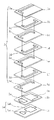
図1は本発明の誘電体フィルタの外観斜視図であり、図2は図1の誘電体フィルタの分解斜視図である。これらの図に示す誘電体フィルタは、積層体1の内部に導体パターンからなるフィルタ素子が配設され、外部に入力端子2、出力端子3及びグランド端子4が被着された構成となっている。
FIG. 1 is an external perspective view of the dielectric filter of the present invention, and FIG. 2 is an exploded perspective view of the dielectric filter of FIG. The dielectric filter shown in these drawings has a configuration in which a filter element made of a conductor pattern is disposed inside the
積層体1は、複数個の誘電体層1a〜1iを積層した構成となっており、誘電体層の材料としては、誘電体セラミック材料、焼結助剤、低融点ガラス材料等が用いられている。誘電体セラミック材料としては、例えばTiO2−Nd2O3−BaTiO3系等の高誘電率のセラミック材料が用いられ、これらのセラミック材料を用いる場合には、焼結温度が低いので、同時焼成により得られる積層体であっても後述するような高導電率材料を内蔵することができるので、インピーダンスの低い伝送線路を備えた部品とすることが可能である。また焼結温度を低くする為に用いる焼結助剤としては、例えば、BiVO4、CuO、Li2O、B2O3等が用いられ、各誘電体層の厚みは、例えば5μm〜300μmに設定される。
The laminated
積層体1の内部に配設される引出電極2a、3a、容量電極4a及び周回パターン5は、誘電体層間に導体パターンとして形成されており、導体パターンの材料としては、Ag、Ag−Pd、Ag−Pt等のAg合金を主成分とする導電材料が用いられ、例えば5μm〜25μmの厚みに形成される。
The
尚、上述した積層体1は、従来周知のセラミックグリーンシート積層法により製作される。具体的には、まずセラミック原料粉末に適当な有機溶剤等を添加・混合して泥漿状になすとともに、従来周知のドクターブレード法等を採用することによってセラミックグリーンシートを形成し、次に得られたセラミックグリーンシートに回路配線(図示せず)やビアホール導体を形成してこれらを積層し、しかる後、この積層体を所定の大きさに分割して、高温で焼成することにより製作される。その後、得られた積層体1の角部には、マイクロクラックの除去や欠けの発生を防止する目的で、バレル研磨等による面取りが施される。
In addition, the laminated
また積層体表面のグランド端子2や入力端子3、出力端子4は、Ag、Ag−Pd、Ag−Pt等のAg合金を主成分とする導電材料等から成り、かかる導電材料を用いて作製した導体ペーストを積層体1の表面に従来周知のディップ法やスクリーン印刷等によって所定パターンに塗布し、これを高温で焼成することによって形成され、これらグランド端子2や入力端子3、出力端子4の表面には、導電性接着剤の濡れ性を良好とするために、更にNiメッキやAuメッキ,Snメッキ,半田メッキ等のメッキ処理が施される。
The
尚、上記積層体1の一主面(上面)には、製品の方向性を示す目的で、積層体1とは異なる色調を呈するマーキングパターン6を形成する場合もある。
In addition, the
本実施形態における誘電体フィルタの内部に配設されるフィルタ素子は、以下に示す構造を有する。 The filter element disposed inside the dielectric filter in the present embodiment has the following structure.
周回パターン5は、複数個のインダクタライン5a〜5gが誘電体層を貫通して形成されるビアホール導体によって接続されたものである。また周回パターン5は、一端側に出力端子3が接続され、他端側に入力端子2が接続されている。尚、ビアホール導体の材料については、上記導体パターンと同じ材料が用いられる。
The
上記周回パターン5の他端側と入力端子2との接続は、引出電極2aを介して行われる。またこの入力側の引出電極2aは、誘電体層1hを介して出力側の引出電極3aの一方の容量形成部3aaと対向して容量成分を形成する役割も有している。
The connection between the other end of the
上記出力側の引出電極3aは、誘電体層1h−1i間に形成されており、他方の容量形成部3abが誘電体層1hを介して容量電極4aと対向して容量成分を形成している。上記容量電極4aは、グランド端子4に接続するグランド電位の導体パターンである。
The output-
尚、本実施形態においては、上記容量電極4aは入力側の引出電極2aと共通の誘電体層1g−1h間に形成されている。
In the present embodiment, the
次に上述した構造のフィルタ素子を有する本実施形態の誘電体フィルタのフィルタ特性について図を用いて説明する。 Next, the filter characteristics of the dielectric filter of the present embodiment having the filter element having the above-described structure will be described with reference to the drawings.
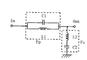
図3は本実施形態の誘電体フィルタの等価回路図、図4はフィルタ特性を示す図であり、同図に示す誘電体フィルタの等価回路はLC並列回路Fpの一端側にLC直列回路Fsを接続したフィルタ素子を配設した構成を有している。 FIG. 3 is an equivalent circuit diagram of the dielectric filter of the present embodiment, and FIG. 4 is a diagram showing filter characteristics. The equivalent circuit of the dielectric filter shown in FIG. 3 has an LC series circuit Fs on one end side of the LC parallel circuit Fp. It has a configuration in which connected filter elements are arranged.
LC並列回路Fpは、上記周回パターン5により形成される誘導成分L1と、引出電極2aと誘電体層1hを挟んで対向する容量形成部3aaとの間に形成される容量成分C1とを有した構成となっている。上記構成のLC並列回路Fpは、一端側に出力端子3が接続され、他端側に入力端子2が接続される。
LC parallel circuit Fp is used, the number and inductive component L1 which is formed by the orbiting
誘導成分L1は、周回パターン5がコイル状を成して強い電磁誘導を有しており、容量成分C1と特定の周波数においてLC並列共振することによりインピーダンスが無限大となり、この周波数においては信号の通過が阻止されるので減衰極Aが形成されることとなる。
The inductive component L 1 has a strong electromagnetic induction in which the
LC直列回路Fsは、上記容量形成部3abの誘導成分L2と、容量形成部3abと誘電体層1hを挟んで対向する容量電極4aとの間に形成される容量成分C2とから構成される。
LC series circuits Fs is the inductive component L 2 of the capacitance forming part 3ab, consists capacitance component C 2 Metropolitan formed between the
誘導成分L2と容量成分C2とは特定の周波数においてLC直列共振することによりインピーダンスが無限小となり、この周波数においては信号がグランド端子に流れて出力端子まで到達しなくなるので減衰極Bが形成されることとなる。 The inductive component L 2 and the capacitive component C 2 have an infinitesimal impedance due to LC series resonance at a specific frequency. At this frequency, the signal flows to the ground terminal and does not reach the output terminal, so that the attenuation pole B is formed. Will be.
上述した本実施形態の誘電体フィルタは、上記減衰極A、Bが形成されることによって、入力端子2から出力端子3までの間に低周波数帯域の通過域と高周波数帯域の広い阻止域(図4参照)を有したEMIノイズフィルタ等のローパスフィルタとして機能することとなる。
In the dielectric filter of the present embodiment described above, the attenuation poles A and B are formed, so that a low frequency band pass band and a high frequency band wide stop band (between the
かかる本実施形態の誘電体フィルタにおいて特徴的な点は、LC並列回路の容量成分C1と、LC直列回路の容量成分C2とが共通の誘電体層1h内に形成されていることである。 The characteristic feature in the dielectric filter according the present embodiment is that the capacitance component C 1 of the LC parallel circuit, and the capacitance component C 2 of the LC series circuits are formed on a common dielectric layer 1h .
これによって誘電体層の積層数を少なくすることができるため、誘電体フィルタの全体構造を小型化することが可能となる。 As a result, the number of laminated dielectric layers can be reduced, so that the overall structure of the dielectric filter can be reduced in size.
またこの場合、2つの減衰極A、Bを形成するそれぞれのLC回路(LC並列回路Fp及びLC直列回路Fs)の容量成分が、共通の誘電体層1h内に形成されているため、誘電体層1hの厚み等がばらついても、この2つのLC回路Fp,Fsの容量成分比は変わらなくなっており、2つの減衰極A、Bの間隔をほとんど変化させることなく阻止域全体の減衰量を安定させることができる。 In this case, since the capacitance components of the respective LC circuits (the LC parallel circuit Fp and the LC series circuit Fs) forming the two attenuation poles A and B are formed in the common dielectric layer 1h, Even if the thickness of the layer 1h varies, the capacitance component ratio of the two LC circuits Fp and Fs does not change, and the attenuation amount of the entire stop band can be reduced without substantially changing the distance between the two attenuation poles A and B. It can be stabilized.
更に本実施形態の誘電体フィルタによれば、LC並列回路Fpの誘導成分L1がLC直列回路Fsの容量電極4aに対して誘電体層を介し対向するように配設されているため、LC並列回路Fpの誘導成分L1である周回パターン5とLC直列回路Fsの容量電極4aとの間にも容量成分が形成されることとなり、これによって良好な周波数特性が得られ易くなる。しかも、1つの容量電極で2つの容量成分が形成されるようになっているため、誘電体フィルタの構成も簡素化される利点もある。
Furthermore, according to the dielectric filter of the present embodiment, since the inductance component L 1 of the LC parallel circuit Fp is disposed so as to face the dielectric layers with respect to the
また更に、出力端子3とLC並列回路Fpの一端部との間には、一端側をグランド端子4に接続したLC直列回路Fsの他端側が接続されているため、出力端子3側のインピーダンスを低くして、外部の回路との整合性を高めることもできる。
Furthermore, since the other end of the LC series circuit Fs having one end connected to the
尚、本発明は上述の実施形態に限定されるものではなく、本発明の要旨を逸脱しない範囲において種々の変更、改良等が可能である。 In addition, this invention is not limited to the above-mentioned embodiment, A various change, improvement, etc. are possible in the range which does not deviate from the summary of this invention.
例えば、上述した実施形態においては積層体の内部に1個のフィルタ素子を有した誘電体フィルタを例にとって説明したが、これに代えて、例えば図5に示すように、積層体の内部に複数のフィルタ素子を有した多連型の誘電体フィルタにも適用可能である。 For example, in the above-described embodiment, the dielectric filter having one filter element in the multilayer body has been described as an example. Instead of this, for example, as shown in FIG. The present invention can also be applied to a multiple-type dielectric filter having the above filter elements.
また上述した実施形態の誘電体フィルタにおいては、LC直列回路を出力端子側に接続するようにしたが、これに代えて、LC直列回路を入力端子側に接続するようにしても構わない。 In the dielectric filter of the above-described embodiment, the LC series circuit is connected to the output terminal side, but instead, the LC series circuit may be connected to the input terminal side.
更に上述した実施形態においては、誘電体層の材質としてセラミック材料を用いるようにしたが、これに代えて、誘電体層の材質として有機材料を用いたり、有機材料中にセラミックフィラーを含有させたセラミック−樹脂の複合材料を用いるようにしても構わない。 Further, in the above-described embodiment, the ceramic material is used as the material of the dielectric layer. Instead, an organic material is used as the material of the dielectric layer, or a ceramic filler is contained in the organic material. A ceramic-resin composite material may be used.
また更に上述した実施形態においては、Ag合金を主成分とする導電材料を用いて導体パターンを形成するようにしたが、これに代えて、AuやCuを主成分とする導電材料を用いて導体パターンを形成するようにしても構わない。これらの導電材料は、積層体表面のグランド電極2や入力端子電極3,出力端子電極4等に用いることができることは言うまでもない。
Furthermore, in the above-described embodiment, the conductive pattern is formed using a conductive material mainly composed of an Ag alloy. Instead, the conductive pattern is formed using a conductive material mainly composed of Au or Cu. A pattern may be formed. Needless to say, these conductive materials can be used for the
1、41・・・積層体
2、42・・・入力端子
2a・・・引出電極(入力側)
3、43・・・出力端子
3a・・・引出電極(出力側)
3aa、3ab・・・容量形成部
4、44・・・グランド端子
4a・・・容量電極
5・・・周回パターン
5a〜5g・・・インダクタパターン
6・・・マーキングパターン
DESCRIPTION OF
3, 43 ...
3aa, 3ab ...
Claims (3)
前記LC並列回路の容量成分C1と前記LC直列回路の容量成分C2とが共通の誘電体層内に形成されていることを特徴とする誘電体フィルタ。 In a dielectric filter in which a filter element in which an LC series circuit is connected to one end side of an LC parallel circuit is disposed inside a laminate formed by laminating a plurality of dielectric layers,
Dielectric filter, characterized in that the capacitance component C 2 of the LC series circuit and capacitance component C 1 of the LC parallel circuit is formed on a common dielectric layer.
Priority Applications (1)
| Application Number | Priority Date | Filing Date | Title |
|---|---|---|---|
| JP2004108877A JP2005295300A (en) | 2004-04-01 | 2004-04-01 | Dielectric filter |
Applications Claiming Priority (1)
| Application Number | Priority Date | Filing Date | Title |
|---|---|---|---|
| JP2004108877A JP2005295300A (en) | 2004-04-01 | 2004-04-01 | Dielectric filter |
Publications (1)
| Publication Number | Publication Date |
|---|---|
| JP2005295300A true JP2005295300A (en) | 2005-10-20 |
Family
ID=35327730
Family Applications (1)
| Application Number | Title | Priority Date | Filing Date |
|---|---|---|---|
| JP2004108877A Pending JP2005295300A (en) | 2004-04-01 | 2004-04-01 | Dielectric filter |
Country Status (1)
| Country | Link |
|---|---|
| JP (1) | JP2005295300A (en) |
Cited By (1)
| Publication number | Priority date | Publication date | Assignee | Title |
|---|---|---|---|---|
| CN104378080A (en) * | 2014-12-02 | 2015-02-25 | 天津航空机电有限公司 | Integrated electromagnetic interference filter |
-
2004
- 2004-04-01 JP JP2004108877A patent/JP2005295300A/en active Pending
Cited By (1)
| Publication number | Priority date | Publication date | Assignee | Title |
|---|---|---|---|---|
| CN104378080A (en) * | 2014-12-02 | 2015-02-25 | 天津航空机电有限公司 | Integrated electromagnetic interference filter |
Similar Documents
| Publication | Publication Date | Title |
|---|---|---|
| EP0793289A1 (en) | Multilayered frequency separator | |
| JP2005159512A (en) | Multilayer band-pass filter | |
| JP2006166136A (en) | Laminated band-pass filter | |
| KR100888019B1 (en) | Capacitor block and laminated plate comprising the same | |
| JP2851966B2 (en) | Multilayer dielectric filter | |
| JPH1028006A (en) | Multilayer resonator, multilayer dielectric filter, and method of adjusting resonance characteristics of multilayer dielectric filter | |
| JPH11225033A (en) | Laminated-type band pass filter | |
| JP2005295300A (en) | Dielectric filter | |
| JP3200954B2 (en) | Composite electronic components | |
| JP4530866B2 (en) | Filter element and electronic module | |
| JP4051252B2 (en) | Noise filter | |
| JP4741566B2 (en) | Noise filter and multilayer noise filter | |
| JP2010062260A (en) | Laminated chip component and its manufacturing method | |
| JP2012146940A (en) | Electronic component and electronic device | |
| JP4280131B2 (en) | Multilayer filter | |
| CN100566148C (en) | noise filter | |
| JPH06163321A (en) | Composite part of high-frequency lc | |
| JPH11205063A (en) | Band stop filter parts | |
| JP4794469B2 (en) | Multilayer dielectric filter | |
| JP2010258743A (en) | Multilayer dielectric filter | |
| JP2006014127A (en) | Balance-unbalance conversion circuit | |
| JP2007214509A (en) | Laminated electronic component | |
| JP2004296927A (en) | Wiring board for storing electronic components | |
| JPH09153703A (en) | Dielectric laminated filter | |
| KR100660971B1 (en) | Ultra-wideband Bandpass Filter Using Low Temperature Co-fired Ceramic Multi-layer Substrate |