JP2005294866A - Method for p-doping of light emitting device - Google Patents
Method for p-doping of light emitting device Download PDFInfo
- Publication number
- JP2005294866A JP2005294866A JP2005168644A JP2005168644A JP2005294866A JP 2005294866 A JP2005294866 A JP 2005294866A JP 2005168644 A JP2005168644 A JP 2005168644A JP 2005168644 A JP2005168644 A JP 2005168644A JP 2005294866 A JP2005294866 A JP 2005294866A
- Authority
- JP
- Japan
- Prior art keywords
- aluminum
- concentration
- gallium arsenide
- interface region
- layer
- Prior art date
- Legal status (The legal status is an assumption and is not a legal conclusion. Google has not performed a legal analysis and makes no representation as to the accuracy of the status listed.)
- Pending
Links
- 238000000034 method Methods 0.000 title claims abstract description 19
- OKTJSMMVPCPJKN-UHFFFAOYSA-N Carbon Chemical compound [C] OKTJSMMVPCPJKN-UHFFFAOYSA-N 0.000 claims abstract description 34
- 229910052799 carbon Inorganic materials 0.000 claims abstract description 34
- 238000005253 cladding Methods 0.000 claims abstract description 23
- 239000000758 substrate Substances 0.000 claims abstract description 14
- FTWRSWRBSVXQPI-UHFFFAOYSA-N alumanylidynearsane;gallanylidynearsane Chemical compound [As]#[Al].[As]#[Ga] FTWRSWRBSVXQPI-UHFFFAOYSA-N 0.000 claims description 35
- 229910052782 aluminium Inorganic materials 0.000 claims description 34
- XAGFODPZIPBFFR-UHFFFAOYSA-N aluminium Chemical compound [Al] XAGFODPZIPBFFR-UHFFFAOYSA-N 0.000 claims description 34
- 238000000151 deposition Methods 0.000 claims description 11
- 238000004519 manufacturing process Methods 0.000 claims description 7
- JLTRXTDYQLMHGR-UHFFFAOYSA-N trimethylaluminium Chemical compound C[Al](C)C JLTRXTDYQLMHGR-UHFFFAOYSA-N 0.000 abstract description 7
- XCZXGTMEAKBVPV-UHFFFAOYSA-N trimethylgallium Chemical compound C[Ga](C)C XCZXGTMEAKBVPV-UHFFFAOYSA-N 0.000 abstract description 7
- 229910052751 metal Inorganic materials 0.000 abstract 2
- 239000002184 metal Substances 0.000 abstract 2
- 150000002739 metals Chemical class 0.000 abstract 2
- 125000002524 organometallic group Chemical group 0.000 description 14
- JBRZTFJDHDCESZ-UHFFFAOYSA-N AsGa Chemical compound [As]#[Ga] JBRZTFJDHDCESZ-UHFFFAOYSA-N 0.000 description 11
- 229910001218 Gallium arsenide Inorganic materials 0.000 description 11
- 239000002019 doping agent Substances 0.000 description 10
- 239000007789 gas Substances 0.000 description 8
- QTQRGDBFHFYIBH-UHFFFAOYSA-N tert-butylarsenic Chemical compound CC(C)(C)[As] QTQRGDBFHFYIBH-UHFFFAOYSA-N 0.000 description 7
- 230000008021 deposition Effects 0.000 description 6
- 239000000463 material Substances 0.000 description 6
- VZGDMQKNWNREIO-UHFFFAOYSA-N tetrachloromethane Chemical group ClC(Cl)(Cl)Cl VZGDMQKNWNREIO-UHFFFAOYSA-N 0.000 description 6
- 230000008569 process Effects 0.000 description 5
- 230000004888 barrier function Effects 0.000 description 4
- 238000001004 secondary ion mass spectrometry Methods 0.000 description 4
- 239000004065 semiconductor Substances 0.000 description 4
- 238000004871 chemical beam epitaxy Methods 0.000 description 3
- 239000000203 mixture Substances 0.000 description 3
- 238000001451 molecular beam epitaxy Methods 0.000 description 3
- GYHNNYVSQQEPJS-UHFFFAOYSA-N Gallium Chemical compound [Ga] GYHNNYVSQQEPJS-UHFFFAOYSA-N 0.000 description 2
- CBENFWSGALASAD-UHFFFAOYSA-N Ozone Chemical compound [O-][O+]=O CBENFWSGALASAD-UHFFFAOYSA-N 0.000 description 2
- 238000006243 chemical reaction Methods 0.000 description 2
- 238000000354 decomposition reaction Methods 0.000 description 2
- 238000009826 distribution Methods 0.000 description 2
- 230000007613 environmental effect Effects 0.000 description 2
- 229910052733 gallium Inorganic materials 0.000 description 2
- 230000009467 reduction Effects 0.000 description 2
- 239000011669 selenium Substances 0.000 description 2
- 229910000530 Gallium indium arsenide Inorganic materials 0.000 description 1
- UFHFLCQGNIYNRP-UHFFFAOYSA-N Hydrogen Chemical compound [H][H] UFHFLCQGNIYNRP-UHFFFAOYSA-N 0.000 description 1
- 229910000673 Indium arsenide Inorganic materials 0.000 description 1
- BUGBHKTXTAQXES-UHFFFAOYSA-N Selenium Chemical compound [Se] BUGBHKTXTAQXES-UHFFFAOYSA-N 0.000 description 1
- XUIMIQQOPSSXEZ-UHFFFAOYSA-N Silicon Chemical compound [Si] XUIMIQQOPSSXEZ-UHFFFAOYSA-N 0.000 description 1
- DKGAVHZHDRPRBM-UHFFFAOYSA-N Tert-Butanol Chemical compound CC(C)(C)O DKGAVHZHDRPRBM-UHFFFAOYSA-N 0.000 description 1
- HCHKCACWOHOZIP-UHFFFAOYSA-N Zinc Chemical compound [Zn] HCHKCACWOHOZIP-UHFFFAOYSA-N 0.000 description 1
- KXNLCSXBJCPWGL-UHFFFAOYSA-N [Ga].[As].[In] Chemical compound [Ga].[As].[In] KXNLCSXBJCPWGL-UHFFFAOYSA-N 0.000 description 1
- MDPILPRLPQYEEN-UHFFFAOYSA-N aluminium arsenide Chemical compound [As]#[Al] MDPILPRLPQYEEN-UHFFFAOYSA-N 0.000 description 1
- 125000004429 atom Chemical group 0.000 description 1
- 230000008901 benefit Effects 0.000 description 1
- 230000015572 biosynthetic process Effects 0.000 description 1
- 230000008859 change Effects 0.000 description 1
- 238000005229 chemical vapour deposition Methods 0.000 description 1
- 230000000779 depleting effect Effects 0.000 description 1
- 238000009792 diffusion process Methods 0.000 description 1
- 238000000407 epitaxy Methods 0.000 description 1
- 125000004435 hydrogen atom Chemical group [H]* 0.000 description 1
- 230000006872 improvement Effects 0.000 description 1
- 238000010348 incorporation Methods 0.000 description 1
- APFVFJFRJDLVQX-UHFFFAOYSA-N indium atom Chemical compound [In] APFVFJFRJDLVQX-UHFFFAOYSA-N 0.000 description 1
- 238000002347 injection Methods 0.000 description 1
- 239000007924 injection Substances 0.000 description 1
- 230000010354 integration Effects 0.000 description 1
- 230000003287 optical effect Effects 0.000 description 1
- 239000000376 reactant Substances 0.000 description 1
- 229910052711 selenium Inorganic materials 0.000 description 1
- 229910052710 silicon Inorganic materials 0.000 description 1
- 239000010703 silicon Substances 0.000 description 1
- JBQYATWDVHIOAR-UHFFFAOYSA-N tellanylidenegermanium Chemical compound [Te]=[Ge] JBQYATWDVHIOAR-UHFFFAOYSA-N 0.000 description 1
- 239000011701 zinc Substances 0.000 description 1
- 229910052725 zinc Inorganic materials 0.000 description 1
Images

Classifications
-
- H—ELECTRICITY
- H01—ELECTRIC ELEMENTS
- H01S—DEVICES USING THE PROCESS OF LIGHT AMPLIFICATION BY STIMULATED EMISSION OF RADIATION [LASER] TO AMPLIFY OR GENERATE LIGHT; DEVICES USING STIMULATED EMISSION OF ELECTROMAGNETIC RADIATION IN WAVE RANGES OTHER THAN OPTICAL
- H01S5/00—Semiconductor lasers
- H01S5/30—Structure or shape of the active region; Materials used for the active region
- H01S5/305—Structure or shape of the active region; Materials used for the active region characterised by the doping materials used in the laser structure
- H01S5/3054—Structure or shape of the active region; Materials used for the active region characterised by the doping materials used in the laser structure p-doping
-
- H—ELECTRICITY
- H01—ELECTRIC ELEMENTS
- H01S—DEVICES USING THE PROCESS OF LIGHT AMPLIFICATION BY STIMULATED EMISSION OF RADIATION [LASER] TO AMPLIFY OR GENERATE LIGHT; DEVICES USING STIMULATED EMISSION OF ELECTROMAGNETIC RADIATION IN WAVE RANGES OTHER THAN OPTICAL
- H01S5/00—Semiconductor lasers
- H01S5/10—Construction or shape of the optical resonator, e.g. extended or external cavity, coupled cavities, bent-guide, varying width, thickness or composition of the active region
- H01S5/18—Surface-emitting [SE] lasers, e.g. having both horizontal and vertical cavities
- H01S5/183—Surface-emitting [SE] lasers, e.g. having both horizontal and vertical cavities having only vertical cavities, e.g. vertical cavity surface-emitting lasers [VCSEL]
- H01S5/18361—Structure of the reflectors, e.g. hybrid mirrors
Landscapes
- Physics & Mathematics (AREA)
- Condensed Matter Physics & Semiconductors (AREA)
- General Physics & Mathematics (AREA)
- Electromagnetism (AREA)
- Optics & Photonics (AREA)
- Semiconductor Lasers (AREA)
- Chemical Vapour Deposition (AREA)
Abstract
Description
本発明は、一般に、半導体材料のドーピングに関し、さらに詳しくは、発光デバイスにおいて用いられる層のドーピングに関する。 The present invention relates generally to doping semiconductor materials, and more particularly to doping layers used in light emitting devices.
近年、垂直キャビティ表面発光レーザ(VCSEL:vertical cavity surface emitting
laser)と呼ばれるレーザ・デバイスに対する関心が高まっている。VCSELデバイスの利点は、このデバイスはウェハに対して垂直な光を発光し、アレイ形成・集積およびオン・ウェハ試験(on-wafer testing)について将来性が高いことである。従来、VCSELデバイスは、その分散ブラグ・リフレクタ(DBR:Distributed Bragg Reflector )において高濃度にドーピングされたアルミニウム・ガリウム砒素層(AlxGa1-xAs/AlyGa1-yAs)を利用する。これらのVCSELデバイスは、一般に、可視(0.65ミクロン)から赤外線(0.98ミクロン)に近い波長の範囲で動作する。よって、DBRは0.57ミクロンよりも長い波長を反射するように作られる。一般に、DBRはp型ドーパントまたはn型ドーパントのいずれかでドーピングされる。これらの層構造の成長は、MOCVD(Metal-organic Chemical Vapor Deposition),MBE(Molecular Beam Epitaxy)またはCBE(Chemical Beam Epitaxy)などのエピタキシャル成長方法によって達成される。
Recently, vertical cavity surface emitting laser (VCSEL)
There is growing interest in laser devices called lasers. The advantage of a VCSEL device is that it emits light perpendicular to the wafer and has great potential for array formation and integration and on-wafer testing. Conventionally, VCSEL device, the distributed Bragg reflector: Using aluminum gallium arsenide layer which is heavily doped in the (DBR Distributed Bragg Reflector) (Al x Ga 1-x As / Al y Ga 1-y As) . These VCSEL devices generally operate in a wavelength range close to visible (0.65 microns) to infrared (0.98 microns). Thus, the DBR is made to reflect wavelengths longer than 0.57 microns. In general, the DBR is doped with either a p-type dopant or an n-type dopant. Growth of these layer structures is achieved by an epitaxial growth method such as MOCVD (Metal-organic Chemical Vapor Deposition), MBE (Molecular Beam Epitaxy), or CBE (Chemical Beam Epitaxy).
しかし、これらのドーピング層を作製するために適切なp型ドーパントを選択することは問題となる。例えば、MOCVDでは亜鉛(Zn)はp型ドーパントとして一般に用いられるが、亜鉛は極めて高い拡散係数を有するので、DBRをドーピングするのに利用できない。別の一般に用いられるp型ドーパント源として、炭素(C)用の四塩化炭素(carbon tetrachloride)(CCl4)があり、これはp型ドーパントである。残念ながら、四塩
化炭素は、現在使用が差し控えられいるオゾン破壊材料であるため、CCl4は利用でき
ない。こられ2つの一般に用いられるp型ドーパントは利用できないので、DBRをp型ドーピングするための別の方法が必要とされることが明白である。
However, selecting an appropriate p-type dopant to produce these doped layers is problematic. For example, zinc (Zn) is commonly used as a p-type dopant in MOCVD, but zinc cannot be used to dope DBR because it has a very high diffusion coefficient. Another commonly used p-type dopant source is carbon tetrachloride (CCl 4 ) for carbon (C), which is a p-type dopant. Unfortunately, CCl 4 is not available because carbon tetrachloride is an ozone depleting material that is currently withheld. Obviously, since these two commonly used p-type dopants are not available, another method for p-type doping the DBR is required.
従来のp型ドーパント材料の使用は製造または環境を考慮した条件を満たさないことがわかる。従って、性能レベルを改善または等しくし、環境問題に影響せず、製造方法を簡単にする、DBRをp型ドーピングする別の方法が極めて望ましい。 It can be seen that the use of conventional p-type dopant materials does not meet the requirements for manufacturing or environmental considerations. Therefore, another method of p-doping DBR that improves or equalizes performance levels, does not affect environmental issues, and simplifies the manufacturing process is highly desirable.
発光デバイス用の被着材料において炭素ドーピング・レベルを制御する方法が提供される。表面を有する基板が設けられる。第1ミラー・スタックがこの基板の表面上に被着される。第1クラッディング領域が第1ミラー・スタック上に被着される。活性層が第1クラッディング層上に被着される。第2クラッディング層が活性層上に被着される。第2ミラー・スタックが第2クラッディング層上に被着され、第2ミラー・スタックの少なくとも第1層は、V族有機金属TBAs(tertiarybutylarsine)とIII族のガリウムおよび
アルミニウム含有有機金属との比率によって制御される炭素ドーピング・レベルを有する。
A method is provided for controlling the carbon doping level in a deposition material for a light emitting device. A substrate having a surface is provided. A first mirror stack is deposited on the surface of this substrate. A first cladding region is deposited on the first mirror stack. An active layer is deposited on the first cladding layer. A second cladding layer is deposited on the active layer. A second mirror stack is deposited on the second cladding layer, and at least the first layer of the second mirror stack comprises a ratio of group V organometallic TBAs (tertiarybutylarsine) to group III gallium and aluminum containing organometallics. Having a carbon doping level controlled by.
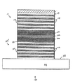
図1において、VCSEL100の構造の簡略拡大断面図の例を示す。一般に、VCSEL100構造は、DBR105,クラッディング領域106,活性領域108,クラッ
ディング領域109およびDBR111など、いくつかの主要部分からなる。VCSEL100構造は、平坦なVCSELデバイス,メサ・エッチ型(mesa-etched) VCSELデバイス,リッジ導波管(ridge-waveguide) VCSELデバイス,発光ダイオードなど、さまざまな構成に処理できることが理解される。さらに、1つのVCSEL構造100のみを基板102の表面101上に示しているが、多数のVCSELデバイスまたは構造を基板102上に形成して、デバイスのアレイを形成できることが理解される。
In FIG. 1, the example of the simplified expanded sectional view of the structure of VCSEL100 is shown. In general, the VCSEL 100 structure is composed of several main parts such as a
一般に、基板102は、n型ドーピング,p型ドーピングまたは半絶縁のガリウム砒素など、任意の適切な半導体材料からなるが、この特定の例では、基板102はガリウム砒素からなる。ガリウム砒素は、それぞれ異なるアルミニウム濃度でアルミニウム・ガリウム砒素の複数の層のエピタキシャル成長を促進するために基板102として用いられる。 In general, the substrate 102 comprises any suitable semiconductor material, such as n-type doping, p-type doping or semi-insulating gallium arsenide, although in this particular example the substrate 102 comprises gallium arsenide. Gallium arsenide is used as substrate 102 to promote epitaxial growth of multiple layers of aluminum gallium arsenide at different aluminum concentrations.
AlxGa1-xAsにおいて異なるアルミニウム組成の交互の層103,104を有するDBR105のエピタキシャル被着は、MOCVD,MBE,CBEなどの最新のエピタキシャル技術によって達成される。これらの技術により、ガリウム砒素,アルミニウム・ガリウム砒素,アルミニウム砒素,インジウム・ガリウム砒素などのさまざまな材料の半導体層のエピタキシャル被着が可能となる。
Epitaxial deposition of
一例として、シリコン(Si),セレニウム(Se)など任意の適切なn型ドーパントでドーピングされたアルミニウム・ガリウム砒素の交互膜または層103,104を有するDBR105のエピタキシャル被着は、基板102の表面101上に被着される。交互層103,104の被着は、VCSEL100構造の第1セットのDBRまたはミラー105を形成する。アルミニウム・ガリウム砒素の交互層103,104の厚さは、一般に、VCSEL100構造が動作するように設計される波長の1/4に設定される。さらに、選択された数の層103,104はVCSEL100について指定された量の反射を行うことが理解される。
As an example, epitaxial deposition of
クラッディング領域106は、交互層103,104を有するDBR105上にエピタキシャル被着される。クラッディング領域106は一般に2つの部分を有するが、これらの部分は図1が煩雑になるのを防ぐため図示されていない。まず第1に、600オングストロームから1,000オングストローム厚の範囲のn型ドーピングされたアルミニウム・ガリウム砒素がDBR105の上に被着される。アルミニウム・ガリウム砒素のドーピングは、一般に1E18cm-3の範囲に維持される。第2に、300オングストロームから700オングストロームの範囲の厚さを有し、より低いアルミニウム組成のドーピングされていないアルミニウム・ガリウム砒素層が、n型ドーピングされたアルミニウム・ガリウム砒素層上に被着される。
The cladding region 106 is epitaxially deposited on the
活性領域108は、クラッディング領域106上にエピタキシャル被着される。活性領域108は、一般に、ガリウム砒素またはインジウム・ガリウム砒素の1つまたはそれ以上の層からなり、アルミニウム・ガリウム砒素またはガリウム砒素障壁層によって分離された量子ウェルを形成する。量子ウェルおよび障壁の両方の公称厚さは、約100オングストロームに維持される。
The
クラッディング領域109は、活性領域108上にエピタキシャル被着される。クラッディング領域109は一般に2つの部分からなるが、これらの部分は図1が煩雑になるのを防ぐために図示されていない。まず第1に、ドーピングされていないアルミニウム・ガリウム砒素層が活性領域108上に被着される。このドーピングされていないアルミニウム・ガリウム砒素層の厚さは、300オングストロームから700オングストロームの範囲である。第2に、p型ドーピングされたアルミニウム・ガリウム砒素層がドーピングされていないアルミニウム・ガリウム砒素層上に被着される。このp型ドーピングされたア
ルミニウム・ガリウム砒素のドーピングは、1E18cm-3レベルに維持される。p型ドーピングされたアルミニウム・ガリウム砒素の厚さは、600オングストロームから1,000オングストロームの範囲である。クラッディング層106,109および活性領域108の厚さは、これらの領域の全光学的厚さがVCSELデバイスの動作波長の1波長または倍数波長に等しくなるように選択される。
A cladding region 109 is epitaxially deposited on the
DBRまたはミラー111は、第2クラッディング領域109上に被着される。ミラーまたはDBR111は、一般に、±5パーセントの公称範囲で、交互アルミニウム濃度がそれぞれ15パーセントおよび80パーセントの、p型ドーピングされたアルミニウム・ガリウム砒素の交互層114,116からなる。交互アルミニウム濃度の対応するp型ドーピング濃度は、1E17cm-3から5E18cm-3の範囲である。交互層114,116の厚さは、VCSEL100が動作するように設計される1/4波長に設定される。さらに、DBR111上のアルミニウム・ガリウム砒素の最後の層である、15パーセント・アルミニウム濃度を有するアルミニウム・ガリウム砒素層117の厚さは、他の交互層114,116で用いられる1/4波長ではなく、3/4波長または1/2波長の厚さに設定される。 The DBR or mirror 111 is deposited on the second cladding region 109. The mirror or DBR 111 generally consists of alternating layers 114, 116 of p-type doped aluminum gallium arsenide with a nominal range of ± 5 percent and alternating aluminum concentrations of 15 percent and 80 percent, respectively. The corresponding p-type doping concentration of the alternating aluminum concentration ranges from 1E17 cm −3 to 5E18 cm −3 . The thickness of the alternating layers 114, 116 is set to a quarter wavelength designed for the VCSEL 100 to operate. Furthermore, the final layer of aluminum gallium arsenide on DBR 111, the thickness of the aluminum gallium arsenide layer 117 having a 15 percent aluminum concentration, is not the quarter wavelength used in the other alternating layers 114 and 116. The thickness is set to 3/4 wavelength or 1/2 wavelength.
AlxGa1-xAs/AlyGa1-yAs、例えば、0.85ミクロンで動作するVCSEL100の場合x=0.15,y=0.80、からなるDBR105,111における反射は、屈折率の差があるために生じる。この屈折率の差は、DBR105,111のそれぞれの交互層103,104および114,116における異なるアルミニウム濃度に起因する。また、AlxGa1-xAs/AlyGa1-yAsのバンドギャップはアルミニウム濃度とともに変化し、DBR105,111内の隣接するAlxGa1-xAs/AlyGa1-yAs層間にヘテロ障壁(heterobarrier)を形成する。このへテロ障壁は、DBR105,
111の直列抵抗をさらに決定し、ヘテロ障壁高さが大きいほど、直列抵抗は大きくなる。直列抵抗を最小限に抑えるため、アルミニウム組成は交互層103,104および114,116間の界面で勾配がつけられる。さらに、ヘテロ障壁および直列抵抗の低下は、界面におけるドーピングの局所的増加によって達成できる。
Al x Ga 1-x As / Al y Ga 1-y As, for example, in the case of VCSEL100 operating at 0.85 microns x = 0.15, the reflection in the y = 0.80, consisting DBR105,111 is refracted This is due to the difference in rates. This difference in refractive index is due to the different aluminum concentrations in the
Further determining the 111 series resistance, the higher the heterobarrier height, the higher the series resistance. The aluminum composition is graded at the interface between the
本発明では、DBRまたはミラー111のp型ドーピングは、真性炭素(intrinsic carbon)(C)によって達成され、この真性炭素は、一般にトリメチルアルミニウム(trimethylaluminium)(TMAl)およびトリメチルガリウム(trimethylgallium)(TMGa)であるアルミニウムおよびガリウムの有機金属源の分解中に解放される。アルミニウム・ガリウム砒素層114,116におけるp型ドーピングの制御は、V族有機金属、例えばTBAs(tertiarybutylarsine)と、III族有機金属、例えばTMAlおよびTMGaと
の比率(V/III比)を変えることによって達成される。TBAsの分解中に生じる水素原子は炭素導入を低減するので、p型ドーピング・レベルはV/III比を変えることによって選択できる。
In the present invention, p-type doping of the DBR or mirror 111 is achieved by intrinsic carbon (C), which is generally trimethylaluminium (TMAl) and trimethylgallium (TMGa). Is released during the decomposition of organometallic sources of aluminum and gallium. Control of p-type doping in the aluminum gallium arsenide layers 114 and 116 is achieved by changing the ratio (V / III ratio) of group V organometallics, such as TBAs (tertiarybutylarsine), to group III organometallics, such as TMAl and TMGa. Achieved. Since hydrogen atoms generated during the decomposition of TBAs reduce carbon incorporation, the p-type doping level can be selected by changing the V / III ratio.
以下で説明するプロセスはAixtron MOCVD エピタキシャル被着システムについてであるが、システムのばらつきや特性差を考慮してプロセス・パラメータを適切に変更することにより、他のエピタキシー・システムも利用できることが理解される。要するに、基板102は、摂氏700度〜900度の範囲の温度および15〜25ミリバールの圧力を有するMOCVDシステムの反応室に入れられる。ただし、本発明の好適な実施例では、反応室の温度は約摂氏720度に設定され、圧力は約20ミリバールに設定される。水素ガスをキャリアとして用いて、反応物質のガスフローまたは蒸気は、10〜60sccmの範囲のTMAl,7〜30sccmの範囲のTMGaおよび70〜110sccmの範囲のTBAsである。広い範囲の温度および圧力下で、同様な結果がMOCVDプロセスで得られることが理解される。よって、ここに示す例は、本発明をわかりやすく説明するように説明のためのみのものである。 The process described below is for an Aixtron MOCVD epitaxial deposition system, but it is understood that other epitaxy systems can be used by appropriately changing process parameters to account for system variability and characteristic differences. . In short, the substrate 102 is placed in a reaction chamber of a MOCVD system having a temperature in the range of 700 to 900 degrees Celsius and a pressure of 15 to 25 mbar. However, in the preferred embodiment of the present invention, the temperature of the reaction chamber is set to about 720 degrees Celsius and the pressure is set to about 20 mbar. Using hydrogen gas as a carrier, the reactant gas flow or vapor is TMAl in the range of 10-60 sccm, TMGa in the range of 7-30 sccm and TBAs in the range of 70-110 sccm. It is understood that similar results are obtained with the MOCVD process under a wide range of temperatures and pressures. Thus, the examples shown here are for illustrative purposes only to illustrate the present invention.
V族含有有機金属とIII族有機金属との適切な比率を与えることにより、15%および80%のアルミニウム濃度で、それぞれ1E16cm-3〜1E17cm-3および3E17cm-3〜3E18cm-3の炭素濃度を有するアルミニウム・ガリウム砒素の膜が得られ、それによりVCSELデバイス構造100のDBRまたはミラー111について適切なp型ドーピング・レベルが得られる。さらに、本発明で具現されるV族およびIII族の有機金属ガスまたは蒸気の適切な比率を利用することにより、VCSEL,発光ダイオードなどの発光デバイスの層のp型ドーピングは、プロセスからCCl4を排除することに
より簡略化される。従って、DBR111の交互のアルミニウム・ガリウム砒素層における適切なp型ドーパント濃度は、リフレクタ領域111の直列抵抗をさらに低減し、DBRまたはミラー111に流れる注入電流(injection current)を可能にする。
By giving an appropriate ratio of Group V containing organometallic Group III organometallic, aluminum concentrations of 15% and 80%, the carbon concentration of each 1E16cm -3 ~1E17cm -3 and 3E17cm -3 ~3E18cm -3 A film of aluminum gallium arsenide is obtained that provides the appropriate p-type doping level for the DBR or mirror 111 of the
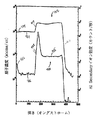
図2は、炭素濃度と、V族含有有機金属ガスまたは蒸気とIII族有機金属ソース・ガスまたは蒸気との比率との関係を示すグラフである。このグラフにおいて、V族有機金属ソース・ガスはTBAsであり、III族有機金属ソース・ガスはトリメチルガリウムおよびトリメチルアルミニウムである。曲線201は、p型ドーピング濃度、すなわち、本発明により被着された15パーセント・アルミニウム濃度を有するアルミニウム・ガリウム砒素層における炭素、を示す。p型ドーピング・レベルの濃度(炭素濃度)は、1E16cm-3から1E17cm-3の範囲であり、V/III比の変化によるアルミニウム・ガリウム砒素における炭素ドーピングの可変濃度を示す。曲線202は、p型ドーピング濃度、すなわち、80パーセント・アルミニウム濃度を有するアルミニウム・ガリウム砒素における炭素、を表す。p型ドーピング・レベルの濃度(炭素濃度)は、3E17cm-3から3E18cm-3の範囲である。従って、V族とIII族有機金属ソース・ガスの適切な比率を選択することにより、適切なドーピング・レベルを有するアルミニウム・ガリウム砒素膜が得られる。さらに、オゾンを破壊する四塩化炭素を必要・使用せずに、p型ドーピング・レベルが生成され、それによりVCSEL,発光ダイオード(LED)などの発光デバイス用のアルミニウム・ガリウム砒素膜を生成する安全かつ効率的な方法が得られる。
FIG. 2 is a graph showing the relationship between the carbon concentration and the ratio of the group V-containing organometallic gas or vapor to the group III organometallic source gas or vapor. In this graph, the Group V organometallic source gas is TBAs, and the Group III organometallic source gas is trimethylgallium and trimethylaluminum.
図3は、SIMS(Secondary Ion Mass Spectrometry)深度分布であり、80パーセン
ト・アルミニウム濃度を有するアルミニウム・ガリウム砒素層上に被着された15パーセント・アルミニウム濃度を有するアルミニウム・ガリウム砒素層におけるオングストローム単位の深さの関数としての立方センチメートル単位の炭素濃度原子を表す。
FIG. 3 is a SIMS (Secondary Ion Mass Spectrometry) depth distribution in Angstrom units in an aluminum gallium arsenide layer having a 15 percent aluminum concentration deposited on an aluminum gallium arsenide layer having an 80 percent aluminum concentration. Represents carbon concentration atoms in cubic centimeters as a function of depth.
ライン401,402は、深度の関数としての炭素濃度およびアルミニウム濃度をそれぞれ表す。ライン401,402の部分403,404は、それぞれ15パーセント・アルミニウム濃度および80パーセント・アルミニウム濃度を有するアルミニウム・ガリウム砒素層の表面またはその付近の炭素およびアルミニウムの濃度レベルを示す。部分406,407は、アルミニウム・ガリウム砒素層のバルクまたは内部におけるそれぞれ炭素およびアルミニウムの濃度レベルを示す。図3R>3からわかるように、炭素およびアルミニウムのバルク濃度は、均等かつ一貫している。しかし、15パーセントおよび80パーセント・アルミニウムを有するアルミニウム・ガリウム砒素層間の界面部分408,409では、炭素濃度はV/III比を低下することにより局所的に増加され、アルミニウム濃度は所望のレベルに調整される。炭素濃度が界面でスパイクが生じるように(尖頭)増加されると、炭素濃度、すなわち、ライン401の部分415は、所望のレベルに調整され、よって2つのアルミニウム・ガリウム砒素層の界面における炭素濃度の可変性が実証される。さらに、DBR111(図2に図示)の炭素濃度の調整により、直列抵抗はさらに低減され、DBR111の性能を向上させる。この性能の向上は、アルミニウム・ガリウム砒素層の界面におけるV/III比を調整して、炭素濃度をスパイクを生じるように増加することによって得られる。従って、界面においてより高いp型ドーピング・レベル
を施すことは、異なるアルミニウム濃度の交互層間のバンドギャップ差によって生じるキャリアの障壁高さの低減に寄与する。
以上、アルミニウム・ガリウム砒素膜の交互層を含む、VCSEL,LEDなどのp型ドーピング層、例えば、DBRの成長およびドーピングの新規な方法が提供されたことが理解される。この方法は、高度に制御可能かつ予測可能に、これらのp型ドーピングされた層を作製する環境的に安全かつ効率的な方法を提供する。さらに、V族とIII族の有機金属ガス・ソースの適切な比率を選択することにより、CCl4を用いずにp型ドーピ
ングが達成され、ドーピング・プロセスを簡略化する。
By now it should be appreciated that a novel method for the growth and doping of p-type doping layers, such as VCSELs, LEDs, etc., including DBR, including alternating layers of aluminum gallium arsenide films, has been provided. This method provides an environmentally safe and efficient way of making these p-type doped layers in a highly controllable and predictable manner. Furthermore, by selecting the appropriate ratio of Group V and Group III organometallic gas sources, p-type doping is achieved without CCl 4 , simplifying the doping process.
100…VCSEL、101…基板の表面、102…基板、103,104…交互層、105…DBR、106…クラッディング領域、108…活性領域、109…クラッディング領域、111…DBR、114,116…交互層、117…アルミニウム・ガリウム砒素層。
DESCRIPTION OF
Claims (4)
表面(101)を有する基板(102)を設ける工程と、
前記基板(102)の前記表面(101)上に第1ミラー・スタック(105)を被着する工程と、
前記第1ミラー・スタック(105)上に第1クラッディング層(106)を被着する工程と、
前記第1クラッディング層(106)上に活性層(108)を被着する工程と、
前記活性層(108)上に第2クラッディング層(109)を被着する工程と、
前記第2クラッディング層(109)上に第2ミラー・スタック(111)を被着する工程と、
複数のアルミニウム・ガリウム砒素の交互の層(114,116)を設ける工程であって、前記交互の層の少なくとも2つ(114,116)は界面領域を画成する、交互の層を設ける工程と、
前記界面領域ではV族有機金属とIII族有機金属の比率を調整することによって前記界面領域で炭素濃度のスパイクを形成する工程とを備え、前記炭素濃度のスパイクは、前記界面領域における炭素濃度が前記界面領域を画成する前記相互の層内部の炭素濃度よりも高くするものである、発光デバイスの製造方法。 A method for manufacturing a light emitting device, comprising:
Providing a substrate (102) having a surface (101);
Depositing a first mirror stack (105) on the surface (101) of the substrate (102);
Depositing a first cladding layer (106) on the first mirror stack (105);
Depositing an active layer (108) on the first cladding layer (106);
Depositing a second cladding layer (109) on the active layer (108);
Depositing a second mirror stack (111) on the second cladding layer (109);
Providing a plurality of alternating layers of aluminum gallium arsenide (114, 116), wherein at least two of the alternating layers (114, 116) define an interfacial region; ,
Forming a carbon concentration spike in the interface region by adjusting a ratio of a Group V organometal to a Group III organometal in the interface region, wherein the carbon concentration spike has a carbon concentration in the interface region. A method for manufacturing a light-emitting device, wherein the concentration is higher than the carbon concentration inside the mutual layers defining the interface region.
Applications Claiming Priority (1)
| Application Number | Priority Date | Filing Date | Title |
|---|---|---|---|
| US27071994A | 1994-07-05 | 1994-07-05 |
Related Parent Applications (1)
| Application Number | Title | Priority Date | Filing Date |
|---|---|---|---|
| JP7189756A Division JPH0832181A (en) | 1994-07-05 | 1995-07-04 | Method for p-type doping luminous |
Publications (1)
| Publication Number | Publication Date |
|---|---|
| JP2005294866A true JP2005294866A (en) | 2005-10-20 |
Family
ID=23032509
Family Applications (2)
| Application Number | Title | Priority Date | Filing Date |
|---|---|---|---|
| JP7189756A Pending JPH0832181A (en) | 1994-07-05 | 1995-07-04 | Method for p-type doping luminous |
| JP2005168644A Pending JP2005294866A (en) | 1994-07-05 | 2005-06-08 | Method for p-doping of light emitting device |
Family Applications Before (1)
| Application Number | Title | Priority Date | Filing Date |
|---|---|---|---|
| JP7189756A Pending JPH0832181A (en) | 1994-07-05 | 1995-07-04 | Method for p-type doping luminous |
Country Status (4)
| Country | Link |
|---|---|
| US (1) | US5547898A (en) |
| JP (2) | JPH0832181A (en) |
| KR (1) | KR100346532B1 (en) |
| DE (1) | DE19523181A1 (en) |
Families Citing this family (14)
| Publication number | Priority date | Publication date | Assignee | Title |
|---|---|---|---|---|
| US6256333B1 (en) | 1997-12-12 | 2001-07-03 | Honeywell Inc. | VCSEL structure insensitive to mobile hydrogen |
| US6301281B1 (en) * | 1998-08-31 | 2001-10-09 | Agilent Technologies, Inc. | Semiconductor laser having co-doped distributed bragg reflectors |
| US20020163688A1 (en) * | 2001-03-26 | 2002-11-07 | Zuhua Zhu | Optical communications system and vertical cavity surface emitting laser therefor |
| US6878958B2 (en) * | 2001-03-26 | 2005-04-12 | Gazillion Bits, Inc. | Vertical cavity surface emitting laser with buried dielectric distributed Bragg reflector |
| US6858519B2 (en) * | 2002-08-14 | 2005-02-22 | Finisar Corporation | Atomic hydrogen as a surfactant in production of highly strained InGaAs, InGaAsN, InGaAsNSb, and/or GaAsNSb quantum wells |
| US7170916B2 (en) * | 2002-10-30 | 2007-01-30 | Finisar Corporation | Selectively etchable heterogeneous composite distributed Bragg reflector |
| US20060215720A1 (en) * | 2005-03-24 | 2006-09-28 | Corzine Scott W | Quantum cascade laser with grating formed by a periodic variation in doping |
| KR100810230B1 (en) | 2005-12-29 | 2008-03-07 | 삼성전자주식회사 | Fabrication method of vertical surface emitting laser light source and vertical surface emitting laser using the same |
| WO2009039354A2 (en) * | 2007-09-19 | 2009-03-26 | Massachusetts Institute Of Technology | Hybrid organic-inorganic dielectric bragg mirrors, and methods of use thereof |
| JP2012134473A (en) * | 2010-11-30 | 2012-07-12 | Sumitomo Chemical Co Ltd | Semiconductor substrate, semiconductor substrate manufacturing method and vertical cavity surface emitting laser |
| WO2012086150A1 (en) * | 2010-12-21 | 2012-06-28 | 住友化学株式会社 | Semiconductor substrate, method for manufacturing semiconductor substrate, and vertical-cavity surface-emitting laser |
| US9991417B2 (en) * | 2015-07-31 | 2018-06-05 | International Business Machines Corporation | Resonant cavity strained III-V photodetector and LED on silicon substrate |
| US10886703B1 (en) * | 2019-06-27 | 2021-01-05 | Lumileds Llc | LED DBR structure with reduced photodegradation |
| US20250219356A1 (en) * | 2022-03-11 | 2025-07-03 | Sony Semiconductor Solutions Corporation | Vertical-cavity surface-emitting laser |
Family Cites Families (10)
| Publication number | Priority date | Publication date | Assignee | Title |
|---|---|---|---|---|
| JPH084169B2 (en) * | 1986-08-28 | 1996-01-17 | ソニー株式会社 | Compound semiconductor laser |
| JPH0754805B2 (en) * | 1986-12-08 | 1995-06-07 | 松下電器産業株式会社 | Vapor growth method of compound semiconductor |
| DE69024246T2 (en) * | 1989-03-31 | 1996-05-30 | Toshiba Kawasaki Kk | Process for producing a thin film semiconductor alloy |
| JP2699661B2 (en) * | 1991-01-08 | 1998-01-19 | 日本電気株式会社 | Semiconductor multilayer reflective film |
| JP2757633B2 (en) * | 1990-12-28 | 1998-05-25 | 日本電気株式会社 | Surface emitting semiconductor laser |
| US5116455A (en) * | 1991-01-24 | 1992-05-26 | Spire Corporation | Process of making strain-free, carbon-doped epitaxial layers and products so made |
| US5226055A (en) * | 1991-09-30 | 1993-07-06 | At&T Bell Laboratories | Devices having repetitive layers |
| US5170407A (en) * | 1991-10-11 | 1992-12-08 | At&T Bell Laboratories | Elimination of heterojunction band discontinuities |
| US5244829A (en) * | 1992-07-09 | 1993-09-14 | Texas Instruments Incorporated | Organometallic vapor-phase epitaxy process using (CH3)3 As and CCl4 for improving stability of carbon-doped GaAs |
| JPH06163985A (en) * | 1992-11-24 | 1994-06-10 | Mitsubishi Kasei Corp | Light emitting and receiving device using III-V group compound |
-
1995
- 1995-06-26 DE DE19523181A patent/DE19523181A1/en not_active Withdrawn
- 1995-07-04 JP JP7189756A patent/JPH0832181A/en active Pending
- 1995-07-05 KR KR1019950019555A patent/KR100346532B1/en not_active Expired - Lifetime
- 1995-09-18 US US08/529,468 patent/US5547898A/en not_active Expired - Lifetime
-
2005
- 2005-06-08 JP JP2005168644A patent/JP2005294866A/en active Pending
Also Published As
| Publication number | Publication date |
|---|---|
| DE19523181A1 (en) | 1996-01-11 |
| US5547898A (en) | 1996-08-20 |
| KR100346532B1 (en) | 2002-11-23 |
| JPH0832181A (en) | 1996-02-02 |
| KR960006167A (en) | 1996-02-23 |
Similar Documents
| Publication | Publication Date | Title |
|---|---|---|
| US7033938B2 (en) | Method of making a long wavelength indium gallium arsenide nitride (InGaAsN) active region | |
| US6207973B1 (en) | Light emitting devices with layered III-V semiconductor structures | |
| JP5018433B2 (en) | Epitaxial wafer for semiconductor light emitting device and semiconductor light emitting device | |
| US6181723B1 (en) | Semiconductor light emitting device with both carbon and group II element atoms as p-type dopants and method for producing the same | |
| JP4259709B2 (en) | Quantum well active layer | |
| US5547898A (en) | Method for p-doping of a light-emitting device | |
| JP2004253801A (en) | InGaAsN device with improved wavelength stability | |
| KR100912622B1 (en) | Method For Manufacturing Semiconductor Optical Device | |
| US6798808B1 (en) | Semiconductor laser device and method of manufacturing same | |
| US5625637A (en) | Surface emitting semiconductor laser and its manufacturing process | |
| JP7095498B2 (en) | Method for manufacturing a vertical resonance type surface emitting laser and a vertical resonance type surface emitting laser | |
| US7915634B2 (en) | Laser diode epitaxial wafer and method for producing same | |
| JP3432909B2 (en) | Semiconductor laser | |
| US5270246A (en) | Manufacturing method of semiconductor multi-layer film and semiconductor laser | |
| US20070241322A1 (en) | Long Wavelength Induim Arsenide Phosphide (InAsP) Quantum Well Active Region And Method For Producing Same | |
| JP3245545B2 (en) | III-V compound semiconductor light emitting device | |
| US20050178318A1 (en) | Method of growing crystal of compound semiconductor and method of manufacturing compound semiconductor device | |
| US6876686B2 (en) | Method of fabricating active layers in a laser utilizing InP-based active regions | |
| JP4636309B2 (en) | Manufacturing method of semiconductor laser device | |
| JP2004165349A (en) | Method for growing compound semiconductor crystal and method for manufacturing light emitting device | |
| JP2009158818A (en) | Epitaxial wafer for semiconductor light emitting device and semiconductor light emitting device | |
| JP2003158079A (en) | GaInNAs crystal growth method and light emitting device manufacturing method | |
| JPH10256160A (en) | Vapor phase growth method of III-V compound semiconductor and semiconductor laser using the same |
Legal Events
| Date | Code | Title | Description |
|---|---|---|---|
| A131 | Notification of reasons for refusal |
Free format text: JAPANESE INTERMEDIATE CODE: A131 Effective date: 20051115 |
|
| A02 | Decision of refusal |
Free format text: JAPANESE INTERMEDIATE CODE: A02 Effective date: 20060425 |