JP2005294791A - Nonvolatile memory and method of manufacturing nonvolatile memory - Google Patents
Nonvolatile memory and method of manufacturing nonvolatile memory Download PDFInfo
- Publication number
- JP2005294791A JP2005294791A JP2004194150A JP2004194150A JP2005294791A JP 2005294791 A JP2005294791 A JP 2005294791A JP 2004194150 A JP2004194150 A JP 2004194150A JP 2004194150 A JP2004194150 A JP 2004194150A JP 2005294791 A JP2005294791 A JP 2005294791A
- Authority
- JP
- Japan
- Prior art keywords
- film
- nonvolatile memory
- insulating layer
- forming
- manufacturing
- Prior art date
- Legal status (The legal status is an assumption and is not a legal conclusion. Google has not performed a legal analysis and makes no representation as to the accuracy of the status listed.)
- Pending
Links
Images


Classifications
-
- H—ELECTRICITY
- H10—SEMICONDUCTOR DEVICES; ELECTRIC SOLID-STATE DEVICES NOT OTHERWISE PROVIDED FOR
- H10B—ELECTRONIC MEMORY DEVICES
- H10B41/00—Electrically erasable-and-programmable ROM [EEPROM] devices comprising floating gates
- H10B41/30—Electrically erasable-and-programmable ROM [EEPROM] devices comprising floating gates characterised by the memory core region
-
- H—ELECTRICITY
- H10—SEMICONDUCTOR DEVICES; ELECTRIC SOLID-STATE DEVICES NOT OTHERWISE PROVIDED FOR
- H10B—ELECTRONIC MEMORY DEVICES
- H10B69/00—Erasable-and-programmable ROM [EPROM] devices not provided for in groups H10B41/00 - H10B63/00, e.g. ultraviolet erasable-and-programmable ROM [UVEPROM] devices
-
- H—ELECTRICITY
- H10—SEMICONDUCTOR DEVICES; ELECTRIC SOLID-STATE DEVICES NOT OTHERWISE PROVIDED FOR
- H10D—INORGANIC ELECTRIC SEMICONDUCTOR DEVICES
- H10D30/00—Field-effect transistors [FET]
- H10D30/60—Insulated-gate field-effect transistors [IGFET]
- H10D30/68—Floating-gate IGFETs
- H10D30/681—Floating-gate IGFETs having only two programming levels
-
- H—ELECTRICITY
- H10—SEMICONDUCTOR DEVICES; ELECTRIC SOLID-STATE DEVICES NOT OTHERWISE PROVIDED FOR
- H10D—INORGANIC ELECTRIC SEMICONDUCTOR DEVICES
- H10D30/00—Field-effect transistors [FET]
- H10D30/60—Insulated-gate field-effect transistors [IGFET]
- H10D30/791—Arrangements for exerting mechanical stress on the crystal lattice of the channel regions
- H10D30/794—Arrangements for exerting mechanical stress on the crystal lattice of the channel regions comprising conductive materials, e.g. silicided source, drain or gate electrodes
-
- H—ELECTRICITY
- H10—SEMICONDUCTOR DEVICES; ELECTRIC SOLID-STATE DEVICES NOT OTHERWISE PROVIDED FOR
- H10D—INORGANIC ELECTRIC SEMICONDUCTOR DEVICES
- H10D30/00—Field-effect transistors [FET]
- H10D30/60—Insulated-gate field-effect transistors [IGFET]
- H10D30/791—Arrangements for exerting mechanical stress on the crystal lattice of the channel regions
- H10D30/795—Arrangements for exerting mechanical stress on the crystal lattice of the channel regions being in lateral device isolation regions, e.g. STI
-
- H—ELECTRICITY
- H10—SEMICONDUCTOR DEVICES; ELECTRIC SOLID-STATE DEVICES NOT OTHERWISE PROVIDED FOR
- H10D—INORGANIC ELECTRIC SEMICONDUCTOR DEVICES
- H10D62/00—Semiconductor bodies, or regions thereof, of devices having potential barriers
- H10D62/10—Shapes, relative sizes or dispositions of the regions of the semiconductor bodies; Shapes of the semiconductor bodies
- H10D62/17—Semiconductor regions connected to electrodes not carrying current to be rectified, amplified or switched, e.g. channel regions
- H10D62/213—Channel regions of field-effect devices
- H10D62/221—Channel regions of field-effect devices of FETs
- H10D62/235—Channel regions of field-effect devices of FETs of IGFETs
Landscapes
- Non-Volatile Memory (AREA)
- Semiconductor Memories (AREA)
Abstract
【課題】
チャネル領域の半導体基板の応力を制御し、メモリセルの電流のオン/オフ比を高くすること、同時に、ゲート酸化膜の劣化を抑制する。
【解決手段】
【0190】
ソース電極27、ドレイン電極28、第1絶縁層11、電荷蓄積層16、第2絶縁層22、及び制御ゲート電極26を具備する不揮発性メモリを用いる。ソース電極27は半導体基板10内に設けられる。ドレイン電極28は半導体基板10内にソース電極27から離れて設けられる。第1絶縁層11はソース電極27とドレイン電極28との間の第1領域8を覆うように設けられる。電荷蓄積層16は第1絶縁層11を介して第1領域8を覆うように設けられる。第2絶縁層22は電荷蓄積層16を覆うように設けられる。制御ゲート電極26は第2絶縁層22を覆うように設けられる。第1領域8における圧縮応力の大きさが50MPa以下である。
【選択図】 図1B【Task】
The stress of the semiconductor substrate in the channel region is controlled to increase the on / off ratio of the memory cell current, and at the same time, the deterioration of the gate oxide film is suppressed.
[Solution]
[0190]
A nonvolatile memory including the source electrode 27, the drain electrode 28, the first insulating layer 11, the charge storage layer 16, the second insulating layer 22, and the control gate electrode 26 is used. The source electrode 27 is provided in the semiconductor substrate 10. The drain electrode 28 is provided in the semiconductor substrate 10 away from the source electrode 27. The first insulating layer 11 is provided so as to cover the first region 8 between the source electrode 27 and the drain electrode 28. The charge storage layer 16 is provided so as to cover the first region 8 via the first insulating layer 11. The second insulating layer 22 is provided so as to cover the charge storage layer 16. The control gate electrode 26 is provided so as to cover the second insulating layer 22. The magnitude of the compressive stress in the first region 8 is 50 MPa or less.
[Selection] Figure 1B
Description
本発明は不揮発性メモリ及び不揮発性メモリの製造方法に関し、特にメモリセルの保持特性を改善した不揮発性メモリ及び不揮発性メモリの製造方法に関する。 The present invention relates to a nonvolatile memory and a method for manufacturing the nonvolatile memory, and more particularly to a nonvolatile memory having improved memory cell retention characteristics and a method for manufacturing the nonvolatile memory.
消去や書き込みをしない限り、一度記憶されたデータが電源を切っても消えないという不揮発性の特性を持つ不揮発性メモリが知られている。この不揮発性メモリのセル構造の例として、1トランジスタ型メモリセル構造がある。このセル構造では、半導体基板上に形成されたゲート絶縁膜上に、電荷蓄積層と制御ゲートとがこの順に積層構造を形成している。電荷蓄積層に蓄積された電荷が記憶されるデータに対応する。1トランジスタ型メモリセル構造は電荷蓄積層の構造により、以下のように分類される。すなわち、電荷蓄積層が層間絶縁膜と導電性を帯びるように不純物が導入された半導体とがこの順に積層した構造である場合、フローティングゲート型セルと呼ばれる。層間絶縁膜と電荷捕獲中心を多く含む絶縁膜がこの順に積層した構造である場合、MONOS(Metal−Oxide−Nitride−Oxide−Semiconductor)型セルと呼ばれる。また、電荷蓄積層が層間絶縁膜と半導体の微粒子を含む絶縁膜とがこの順に積層した構造である場合、ナノクリスタル型セルと呼ばれる。この半導体の微粒子を含む絶縁膜は、さらに金属の微粒子を含む場合もある。さらに、電荷蓄積層が強誘電体、又は、強誘電体、金属電極がこの順に積層した構造である場合、MF(M)IS(Metal−Ferroelectrics−(Metal)−Insulator−Semiconductor)型セルと呼ばれる。MFMIS型セルを用いた不揮発性メモリにおいては、電荷蓄積層に含まれる強誘電体の自発分極の方向が記憶されるデータに対応する。 There is known a nonvolatile memory having a nonvolatile characteristic that data stored once is not erased even if the power is turned off unless erased or written. As an example of the cell structure of this nonvolatile memory, there is a one-transistor type memory cell structure. In this cell structure, a charge storage layer and a control gate form a laminated structure in this order on a gate insulating film formed on a semiconductor substrate. The charge stored in the charge storage layer corresponds to the stored data. The one-transistor memory cell structure is classified as follows according to the structure of the charge storage layer. That is, when the charge storage layer has a structure in which an interlayer insulating film and a semiconductor into which impurities are introduced so as to be conductive are stacked in this order, it is called a floating gate type cell. A structure in which an interlayer insulating film and an insulating film including many charge trapping centers are stacked in this order is referred to as a MONOS (Metal-Oxide-Nitride-Oxide-Semiconductor) type cell. When the charge storage layer has a structure in which an interlayer insulating film and an insulating film containing semiconductor fine particles are stacked in this order, it is called a nanocrystal cell. The insulating film containing semiconductor fine particles may further contain metal fine particles. Furthermore, when the charge storage layer has a ferroelectric structure, or a structure in which a ferroelectric substance and a metal electrode are laminated in this order, it is called an MF (M) IS (Metal-Ferroelectrics- (Metal) -Insulator-Semiconductor) type cell. . In the nonvolatile memory using the MFMIS type cell, the direction of spontaneous polarization of the ferroelectric contained in the charge storage layer corresponds to stored data.
これらの1トランジスタ型メモリセル構造をとる不揮発性メモリの共通点は、データの書き込みや読み出しが、セル構造周辺の半導体基板上に形成された、ソース、ドレイン及び積層構造の制御ゲートを用いて、ソースとドレインの間のチャネル領域に流れる電流を制御することで行われるということである。したがって、これらの構造を用いた不揮発性メモリの高性能化、高信頼性化を実現するには、その製造プロセスにおいて、チャネル領域、ゲート絶縁膜の諸物性量を十分に制御することが必須である。 The common point of these non-volatile memories having a one-transistor memory cell structure is that data writing and reading are performed using a source, drain, and stacked structure control gate formed on a semiconductor substrate around the cell structure. This is done by controlling the current flowing in the channel region between the source and drain. Therefore, in order to achieve high performance and high reliability of nonvolatile memories using these structures, it is essential to fully control the physical properties of the channel region and gate insulating film in the manufacturing process. is there.
他方、メモリの大容量化、小型化の要請から、メモリセルの微細化が追求されている。これに伴い、素子分離に起因する応力が、チャネル領域に及ぶようになる。浅いトレンチによる素子分離の場合、トレンチに埋設される絶縁膜はチャネル領域において、基板表面に平行方向の圧縮応力を及ぼす。チャネル領域に強い圧縮応力が印加されると、電子の移動度が低下する。このとき、メモリセルの電流のオン/オフ比が低下するため、ゲート酸化膜を介して電荷蓄積層に出し入れする電荷量を多くしなくてはならない。出し入れする電荷量が多くなると、ゲート酸化膜の劣化が著しくなり、オン電流の減少や、保持特性の劣化が生じる。また、浅いトレンチによる素子分離に起因する圧縮応力はチャネル領域とともにゲート絶縁膜にも同様に印加される。ゲート絶縁膜に強い圧縮応力が印加されると、ゲート絶縁膜中に存在する、電子トラップの活性化エネルギーが減少する。このことは電子トラップに捕獲されていた電子が放出されやすくなること、したがって、トランジスタのしきい値電圧が変動しやすくなることを意味している。これは保持特性劣化の一因となる。 On the other hand, miniaturization of memory cells has been pursued due to demands for increasing the capacity and size of memories. Along with this, stress due to element isolation reaches the channel region. In the case of element isolation by a shallow trench, the insulating film buried in the trench exerts a compressive stress in a direction parallel to the substrate surface in the channel region. When strong compressive stress is applied to the channel region, the mobility of electrons decreases. At this time, since the on / off ratio of the current of the memory cell is lowered, the amount of charge to and from the charge storage layer through the gate oxide film must be increased. When the amount of charge to be taken in and out increases, the gate oxide film is remarkably deteriorated, the on-current is reduced, and the retention characteristics are deteriorated. Further, the compressive stress resulting from the element isolation by the shallow trench is similarly applied to the gate insulating film as well as the channel region. When a strong compressive stress is applied to the gate insulating film, the activation energy of the electron trap existing in the gate insulating film is reduced. This means that the electrons trapped in the electron trap are likely to be emitted, and therefore the threshold voltage of the transistor is likely to fluctuate. This contributes to deterioration of holding characteristics.
以上ではチャネル領域やゲート絶縁膜に対する圧縮応力の影響について述べたが、引張応力も、メモリ動作に影響を与える。強い引張応力がチャネル領域及びゲート絶縁膜に印加されると、ゲート絶縁膜と半導体基板との界面に存在するダングリングボンド−水素原子等の結合が切断されやすくなる。したがって、強い引張応力下では、応力なしの場合に比べゲート絶縁膜/半導体基板界面の界面準位数が多い。このことは、強い引張応力下では界面準位の回復によるトランジスタのしきい値電圧の変動が大きくなることを意味している。よって、強い引張応力も保持特性劣化の一因である。 In the above, the influence of the compressive stress on the channel region and the gate insulating film has been described, but the tensile stress also affects the memory operation. When a strong tensile stress is applied to the channel region and the gate insulating film, dangling bonds-hydrogen atoms and the like existing at the interface between the gate insulating film and the semiconductor substrate are likely to be broken. Therefore, under a strong tensile stress, the number of interface states at the gate insulating film / semiconductor substrate interface is larger than that without stress. This means that the fluctuation of the threshold voltage of the transistor due to the recovery of the interface state becomes large under a strong tensile stress. Therefore, a strong tensile stress is also a cause of deterioration of holding characteristics.
したがって、保持特性劣化を抑制し、高信頼化された不揮発性メモリを実現するには、チャネル領域における半導体基板応力の絶対値を低減する技術が望まれる。この技術により、メモリセルの電流のオン/オフ比を高くすること、ゲート酸化膜の劣化を抑制することメモリセルの特性を維持することが可能となる。その結果、書き換え回数を向上することや、多値メモリに適するセル特性を得ることが可能となる。 Therefore, a technique for reducing the absolute value of the semiconductor substrate stress in the channel region is desired in order to suppress the retention characteristic deterioration and realize a highly reliable nonvolatile memory. This technique makes it possible to increase the on / off ratio of the current of the memory cell and to suppress the deterioration of the gate oxide film and maintain the characteristics of the memory cell. As a result, it is possible to improve the number of rewrites and obtain cell characteristics suitable for a multilevel memory.
関連する技術として、特開平8−31962号公報に不揮発性半導体記憶装置の製造方法の技術が開示されている。この発明の目的は、ゲート絶縁膜特性の劣化をもたらさないような層間絶縁膜を実現することにある。この不揮発性半導体記憶装置の製造方法は、電気的に書き換え可能な不揮発性半導体記憶装置の製造方法である。ここで、不揮発性半導体記憶装置は、第1導電型を有する半導体基板にゲート絶縁膜を介して設けられた浮遊ゲート電極と、その浮遊ゲート電極上に少なくとも一部分が積層される形で層間絶縁膜を介して設けられた制御ゲート電極と、その半導体基板内に互いに分離して設けられた第2導電型のソース、ドレイン領域を備える。そして、その層間絶縁膜として化学気相成長法により単層酸化シリコン膜を形成することを特徴とする。本公報では、この技術により、層間絶縁膜の応力が緩和されるため、ゲート絶縁膜の劣化が低減されると記載されている。 As a related technique, Japanese Patent Application Laid-Open No. 8-31962 discloses a technique for manufacturing a nonvolatile semiconductor memory device. An object of the present invention is to realize an interlayer insulating film which does not cause deterioration of gate insulating film characteristics. This method for manufacturing a nonvolatile semiconductor memory device is a method for manufacturing an electrically rewritable nonvolatile semiconductor memory device. Here, the nonvolatile semiconductor memory device includes a floating gate electrode provided on a semiconductor substrate having a first conductivity type via a gate insulating film, and an interlayer insulating film in which at least a part is stacked on the floating gate electrode. And a second conductivity type source / drain region provided separately from each other in the semiconductor substrate. A single-layer silicon oxide film is formed as the interlayer insulating film by chemical vapor deposition. In this publication, this technique describes that the stress of the interlayer insulating film is relieved, so that the deterioration of the gate insulating film is reduced.
従って、本発明の目的は、チャネル領域における半導体基板の応力の絶対値を抑制することが可能な不揮発性メモリ及び不揮発性メモリの製造方法を提供することにある。 Accordingly, an object of the present invention is to provide a nonvolatile memory and a method for manufacturing the nonvolatile memory that can suppress the absolute value of the stress of the semiconductor substrate in the channel region.
また、本発明の他の目的は、メモリセルの電流のオン/オフ比を高くすることができる不揮発性メモリの構造及び不揮発性メモリの製造方法を提供することにある。 Another object of the present invention is to provide a non-volatile memory structure and a non-volatile memory manufacturing method capable of increasing the on / off ratio of the current of a memory cell.
本発明の更に他の目的は、ゲート酸化膜の劣化を抑制することができる不揮発性メモリの構造及び不揮発性メモリの製造方法を提供することにある。 Still another object of the present invention is to provide a non-volatile memory structure and a non-volatile memory manufacturing method capable of suppressing deterioration of a gate oxide film.
本発明の別の目的は、メモリセルの特性を維持し、書き換え回数を向上することが可能な不揮発性メモリの構造及び不揮発性メモリの製造方法を提供することにある。 Another object of the present invention is to provide a non-volatile memory structure and a non-volatile memory manufacturing method capable of maintaining the characteristics of memory cells and improving the number of rewrites.
本発明の更に別の目的は、多値メモリに適するセル特性を得ることができる不揮発半導体メモリの構造及び不揮発性メモリの製造方法を提供することにある。 Still another object of the present invention is to provide a non-volatile semiconductor memory structure and a non-volatile memory manufacturing method capable of obtaining cell characteristics suitable for a multi-level memory.
以下に、発明を実施するための最良の形態で使用される番号・符号を用いて、課題を解決するための手段を説明する。これらの番号・符号は、特許請求の範囲の記載と発明を実施するための最良の形態との対応関係を明らかにするために括弧付きで付加されたものである。ただし、それらの番号・符号を,特許請求の範囲に記載されている発明の技術的範囲の解釈に用いてはならない。 Hereinafter, means for solving the problem will be described using the numbers and symbols used in the best mode for carrying out the invention. These numbers and symbols are added in parentheses in order to clarify the correspondence between the description of the claims and the best mode for carrying out the invention. However, these numbers and symbols should not be used for the interpretation of the technical scope of the invention described in the claims.
上記課題を解決するために、本発明の不揮発性メモリは、ソース電極(27)と、ドレイン電極(28)と、第1絶縁層(11)と、電荷蓄積層(16)と、第2絶縁層(22)と、制御ゲート電極(26)とを具備する。ソース電極(27)は、半導体基板(10)内に設けられている。ドレイン電極(28)は、半導体基板(10)内にソース電極(27)から離れて設けられている。第1絶縁層(11)は、ソース電極(27)及びドレイン電極(28)の少なくとも一部、及び、ソース電極(27)とドレイン電極(28)との間の第1領域(8)を覆うように設けられている。電荷蓄積層(16)は、第1絶縁層(11)を介して第1領域(8)を覆うように設けられている。第2絶縁層(22)は、電荷蓄積層(16)を覆うように設けられている。制御ゲート電極(26)は、第2絶縁層(22)を覆うように設けられている。第1領域(8)における圧縮応力の大きさが、50MPa以下である。 In order to solve the above problems, a nonvolatile memory according to the present invention includes a source electrode (27), a drain electrode (28), a first insulating layer (11), a charge storage layer (16), and a second insulating layer. A layer (22) and a control gate electrode (26) are provided. The source electrode (27) is provided in the semiconductor substrate (10). The drain electrode (28) is provided in the semiconductor substrate (10) apart from the source electrode (27). The first insulating layer (11) covers at least a part of the source electrode (27) and the drain electrode (28) and the first region (8) between the source electrode (27) and the drain electrode (28). It is provided as follows. The charge storage layer (16) is provided so as to cover the first region (8) through the first insulating layer (11). The second insulating layer (22) is provided so as to cover the charge storage layer (16). The control gate electrode (26) is provided so as to cover the second insulating layer (22). The magnitude of the compressive stress in the first region (8) is 50 MPa or less.
上記の不揮発性メモリにおいて、第1領域(8)における引張応力の大きさが、50MPa以下である。 In the above nonvolatile memory, the magnitude of the tensile stress in the first region (8) is 50 MPa or less.
上記の不揮発性メモリにおいて、制御ゲート電極(26)は、第2絶縁層(22)側から順に半導体膜(24)、金属膜(25)の積層構造を有する。 In the above nonvolatile memory, the control gate electrode (26) has a stacked structure of a semiconductor film (24) and a metal film (25) in this order from the second insulating layer (22) side.
上記の不揮発性メモリにおいて、金属膜(25)は、タングステン、タンタル、モリブデン、窒化タングステン、窒化タンタル、及び窒化モリブデンのうちの少なくとも一つを含む。 In the above nonvolatile memory, the metal film (25) includes at least one of tungsten, tantalum, molybdenum, tungsten nitride, tantalum nitride, and molybdenum nitride.
上記の不揮発性メモリにおいて、半導体基板(10)の少なくとも一部が表面側から順にシリコン、シリコンゲルマニウムの積層構造を有する。 In the above nonvolatile memory, at least a part of the semiconductor substrate (10) has a laminated structure of silicon and silicon germanium in order from the surface side.
上記の不揮発性メモリにおいて、ソース電極(27)及びドレイン電極(28)の少なくとも一方が、炭素が添加されたシリコンゲルマニウム(29)及び炭素が添加されたシリコン(29)のうちの少なくとも一方を含む。 In the above nonvolatile memory, at least one of the source electrode (27) and the drain electrode (28) includes at least one of silicon germanium (29) to which carbon is added and silicon (29) to which carbon is added. .
上記の不揮発性メモリにおいて、電荷蓄積層(16)が、半導体薄膜である。 In the above nonvolatile memory, the charge storage layer (16) is a semiconductor thin film.
上記の不揮発性メモリにおいて、電荷蓄積層(16)が電荷捕獲中心を含有する絶縁層である。 In the above nonvolatile memory, the charge storage layer (16) is an insulating layer containing charge trapping centers.
上記の不揮発性メモリにおいて、その電荷捕獲中心を含有する絶縁層は、窒化シリコン、酸化アルミニウム、酸窒化アルミニウム、酸化ハフニウム、酸窒化ハフニウム、酸化シリコンハフニウム、酸窒化シリコンハフニウム、酸化ジルコニウム、酸窒化ジルコニウム、酸化シリコンジルコニウム、及び、酸窒化シリコンジルコニウムのうちの少なくとも一つである。 In the above nonvolatile memory, the insulating layer containing the charge trapping center is silicon nitride, aluminum oxide, aluminum oxynitride, hafnium oxide, hafnium oxynitride, silicon hafnium oxide, silicon hafnium oxynitride, zirconium oxide, zirconium oxynitride , Silicon zirconium oxide, and silicon zirconium oxynitride.
上記の不揮発性メモリにおいて、電荷蓄積層(16)は、絶縁体薄膜(16a)と半導体微粒子(16b)とから形成される。 In the above nonvolatile memory, the charge storage layer (16) is formed of an insulator thin film (16a) and semiconductor fine particles (16b).
上記の不揮発性メモリにおいて、第2絶縁層(22)を持たず、かつ、電荷蓄積層(16)が強誘電体ある。 In the above nonvolatile memory, the second insulating layer (22) is not provided, and the charge storage layer (16) is a ferroelectric substance.
上記の不揮発性メモリにおいて、第2絶縁層(22)を持たず、かつ、電荷蓄積層(16)が第1絶縁層側から順に金属、強誘電体の積層構造を有する。 In the above nonvolatile memory, the second insulating layer (22) is not provided, and the charge storage layer (16) has a stacked structure of metal and ferroelectric in order from the first insulating layer side.
上記の不揮発性メモリにおいて、第1絶縁層(11)と制御ゲート電極(26)とを覆うように設けられた第3絶縁層(35)とを更に具備する。 The nonvolatile memory further includes a third insulating layer (35) provided so as to cover the first insulating layer (11) and the control gate electrode (26).
上記の不揮発性メモリにおいて、第3絶縁膜(35)は、引張応力を有する。 In the above nonvolatile memory, the third insulating film (35) has a tensile stress.
上記の不揮発性メモリにおいて、第3絶縁膜(35)は、SiN膜、SiON膜、SiCN膜、AlO膜、及びAlSiN膜の少なくとも一つを含む。 In the above nonvolatile memory, the third insulating film (35) includes at least one of a SiN film, a SiON film, a SiCN film, an AlO film, and an AlSiN film.
上記の不揮発性メモリにおいて、電荷蓄積層(16)、第2絶縁層(22)及び制御ゲート電極(26)の側面を覆い、下部が第1絶縁層(11)に接するように設けられたサイドウォール(30)を更に具備する。サイドウォール(30)は、第1絶縁層(11)に概ね平行な第1層と、その側面に概ね平行な第2層とを備えている。その第1層は、引張応力を有する。 In the above nonvolatile memory, the side provided so as to cover the side surfaces of the charge storage layer (16), the second insulating layer (22), and the control gate electrode (26), and the lower portion is in contact with the first insulating layer (11). A wall (30) is further provided. The sidewall (30) includes a first layer substantially parallel to the first insulating layer (11) and a second layer substantially parallel to the side surface. The first layer has a tensile stress.
上記の不揮発性メモリにおいて、その第1層は、SiN膜、SiON膜、SiCN膜、AlO膜、及びAlSiN膜の少なくとも一つを含む。 In the above nonvolatile memory, the first layer includes at least one of a SiN film, a SiON film, a SiCN film, an AlO film, and an AlSiN film.
上記の不揮発性メモリにおいて、半導体基板(10)内に設けられた素子分離絶縁部(20)を更に具備する。 The nonvolatile memory further includes an element isolation insulating part (20) provided in the semiconductor substrate (10).
上記の不揮発性メモリにおいて、素子分離絶縁部(20)は、少なくとも一部にシリコン窒化膜を含むトレンチ溝(19)である。 In the above nonvolatile memory, the element isolation insulating portion (20) is a trench groove (19) including a silicon nitride film at least partially.
上記課題を解決するために、本発明の不揮発性メモリの製造方法は、半導体基板(10)上に第1絶縁層(11)を形成するステップと、半導体基板(10)の第1領域(8)上の第1絶縁層(11)を覆うように、電荷蓄積膜(16)、第2絶縁層(22)及び制御ゲート電極(26)がこの順で積層された上部構造を形成するステップと、半導体基板(10)内において、ソース電極(27)及びドレイン電極(28)を、各々が第1領域(8)に接し、互いに離れるように形成するステップとを具備する。その上部構造を形成するステップは、不揮発性メモリ製造後の第1領域(8)における圧縮応力の大きさが50MPa以下、あるいは引張応力の大きさが50MPa以下であるように、制御ゲート電極(26)として第2絶縁層(22)側から順に半導体膜(24)、金属膜(25)の積層構造を形成するステップを備える。 In order to solve the above problems, a method for manufacturing a nonvolatile memory according to the present invention includes a step of forming a first insulating layer (11) on a semiconductor substrate (10), and a first region (8) of the semiconductor substrate (10). ) Forming an upper structure in which the charge storage film (16), the second insulating layer (22), and the control gate electrode (26) are stacked in this order so as to cover the first insulating layer (11) on the upper side) Forming a source electrode (27) and a drain electrode (28) in the semiconductor substrate (10) so as to be in contact with the first region (8) and away from each other. The step of forming the superstructure includes the control gate electrode (26) so that the magnitude of the compressive stress in the first region (8) after manufacturing the nonvolatile memory is 50 MPa or less, or the magnitude of the tensile stress is 50 MPa or less. ) As a stacked structure of a semiconductor film (24) and a metal film (25) in order from the second insulating layer (22) side.
上記の不揮発性メモリの製造方法において、金属膜(25)は、タングステン、タンタル、モリブデン、窒化タングステン、窒化タンタル、及び窒化モリブデンのうちの少なくとも一つを含む膜である。 In the above method for manufacturing a nonvolatile memory, the metal film (25) is a film including at least one of tungsten, tantalum, molybdenum, tungsten nitride, tantalum nitride, and molybdenum nitride.
上記課題を解決するために、本発明の不揮発性メモリの製造方法は、半導体基板(10)上に、シリコンゲルマニウム膜(10b)とシリコン膜(10a)とがこの順に積層された積層構造を形成するステップと、その積層構造上に、第1絶縁層(11)を形成するステップと、半導体基板(10)の第1領域(8)上の第1絶縁層(11)を覆うように、電荷蓄積膜(16)、第2絶縁層(22)及び制御ゲート電極(26)がこの順で積層された上部構造を形成するステップと、半導体基板(10)内において、ソース電極(27)及びドレイン電極(28)を、各々が第1領域(8)に接し、互いに離れるように形成するステップとを具備する。その積層構造は、不揮発性メモリ製造後の第1領域(8)における圧縮応力の大きさが50MPa以下、あるいは引張応力の大きさが50MPa以下となるように形成される。 In order to solve the above-described problems, a method for manufacturing a nonvolatile memory according to the present invention forms a stacked structure in which a silicon germanium film (10b) and a silicon film (10a) are stacked in this order on a semiconductor substrate (10). A step of forming a first insulating layer (11) on the stacked structure, and a charge so as to cover the first insulating layer (11) on the first region (8) of the semiconductor substrate (10). A step of forming an upper structure in which a storage film (16), a second insulating layer (22), and a control gate electrode (26) are stacked in this order; and a source electrode (27) and a drain in the semiconductor substrate (10) Forming electrodes (28), each in contact with the first region (8) and away from each other. The stacked structure is formed such that the magnitude of the compressive stress in the first region (8) after manufacturing the nonvolatile memory is 50 MPa or less, or the magnitude of the tensile stress is 50 MPa or less.
上記課題を解決するために、本発明の不揮発性メモリの製造方法は、シリコン基板(10)上に、第1絶縁層(11)を形成するステップと、シリコン基板(10)の第1領域(8)上の第1絶縁層(11)を覆うように、電荷蓄積膜(16)、第2絶縁層(22)及び制御ゲート電極(26)がこの順で積層された上部構造を形成するステップと、シリコン基板(10)内のソース電極(27)及びドレイン電極(28)となる部分の少なくとも一部に、炭素を添加したシリコンゲルマニウム膜(29)及び炭素を添加したシリコン膜(29)の少なくとも一方を形成するステップと、シリコン基板(10)内においてソース電極(27)及びドレイン電極(28)を、各々が第1領域(8)に接し、互いに離れるように形成するステップとを具備する。炭素を添加されたシリコンゲルマニウム膜(29)及び炭素を添加されたシリコン膜(29)は、不揮発性メモリ製造後の第1領域(8)における圧縮応力の大きさが50MPa以下、あるいは引張応力の大きさが50MPa以下であるように形成される。 In order to solve the above problems, a method for manufacturing a nonvolatile memory according to the present invention includes a step of forming a first insulating layer (11) on a silicon substrate (10), and a first region ( 8) A step of forming an upper structure in which the charge storage film (16), the second insulating layer (22), and the control gate electrode (26) are laminated in this order so as to cover the first insulating layer (11) on the upper side. And a silicon germanium film (29) to which carbon is added and a silicon film (29) to which carbon is added to at least a part of portions to be the source electrode (27) and the drain electrode (28) in the silicon substrate (10). Forming at least one, and forming a source electrode (27) and a drain electrode (28) in the silicon substrate (10) so as to be in contact with the first region (8) and away from each other. Comprising a. The silicon germanium film (29) to which carbon is added and the silicon film (29) to which carbon is added have a compressive stress of 50 MPa or less or a tensile stress in the first region (8) after manufacturing the nonvolatile memory. It is formed so that the size is 50 MPa or less.
上記課題を解決するために、本発明の不揮発性メモリの製造方法は、半導体基板(10)上に、素子分離絶縁部(20)を形成するステップと、素子分離絶縁部(20)以外の半導体基板(10)上に第1絶縁層(11)を形成するステップと、半導体基板(10)の第1領域(8)上の第1絶縁層(11)を覆うように、電荷蓄積膜(16)、第2絶縁層(22)及び制御ゲート電極(26)がこの順で積層された上部構造を形成するステップと、半導体基板(10)内において,ソース電極(27)及びドレイン電極(28)を、各々が第1領域(8)に接し、互いに離れるように形成するステップとを具備する。素子分離絶縁部(20)を形成するステップは、不揮発性メモリ製造後の第1領域(8)における圧縮応力の大きさが50MPa以下、あるいは引張応力の大きさが50MPa以下であるように、素子分離絶縁部(20)の少なくとも一部を窒化シリコン膜が含まれるトレンチ溝(19)で形成するステップを備える。 In order to solve the above problems, a method for manufacturing a nonvolatile memory according to the present invention includes a step of forming an element isolation insulating part (20) on a semiconductor substrate (10), and a semiconductor other than the element isolation insulating part (20). A step of forming a first insulating layer (11) on the substrate (10) and a charge storage film (16) so as to cover the first insulating layer (11) on the first region (8) of the semiconductor substrate (10). ), A step of forming an upper structure in which the second insulating layer (22) and the control gate electrode (26) are laminated in this order, and a source electrode (27) and a drain electrode (28) in the semiconductor substrate (10). Are formed so that each is in contact with the first region (8) and away from each other. The step of forming the element isolation insulating portion (20) is performed so that the magnitude of the compressive stress in the first region (8) after manufacturing the nonvolatile memory is 50 MPa or less, or the magnitude of the tensile stress is 50 MPa or less. Forming at least a part of the isolation insulating part (20) with a trench groove (19) including a silicon nitride film.
上記課題を解決するために、本発明の不揮発性メモリの製造方法は、半導体基板(10)上に第1絶縁層(11)を形成するステップと、半導体基板(10)の第1領域(8)上の第1絶縁層(11)を覆うように、電荷蓄積膜(16)、第2絶縁層(22)及び制御ゲート電極(26)がこの順で積層された上部構造を形成するステップと、半導体基板(10)内において、ソース電極(27)及びドレイン電極(28)を、各々が第1領域(8)に接し、互いに離れるように形成するステップと、第1絶縁層(11)上及びその上部構造上に、第1領域(8)における圧縮応力の大きさが50MPa以下、あるいは引張応力の大きさが50MPa以下であるように第3絶縁層(35)を形成するステップとを具備する。 In order to solve the above problems, a method for manufacturing a nonvolatile memory according to the present invention includes a step of forming a first insulating layer (11) on a semiconductor substrate (10), and a first region (8) of the semiconductor substrate (10). ) Forming an upper structure in which the charge storage film (16), the second insulating layer (22), and the control gate electrode (26) are stacked in this order so as to cover the first insulating layer (11) on the upper side) And forming a source electrode (27) and a drain electrode (28) in the semiconductor substrate (10) so as to be in contact with the first region (8) and away from each other, and on the first insulating layer (11). And forming a third insulating layer (35) on the upper structure so that the magnitude of the compressive stress in the first region (8) is 50 MPa or less, or the magnitude of the tensile stress is 50 MPa or less. To do.
上記の不揮発性メモリの製造方法において、第3絶縁層(35)を形成するステップは、シラン又はジクロルシランを原料ガスとして、CVD法で600℃以上の温度にて製膜するステップを備える。 In the method for manufacturing a nonvolatile memory, the step of forming the third insulating layer (35) includes a step of forming a film at a temperature of 600 ° C. or higher by a CVD method using silane or dichlorosilane as a source gas.
上記の不揮発性メモリの製造方法において、第3絶縁層(35)を形成するステップは、モノメチルシランとヒドラジンを原料ガスとして、CVD法で製膜するステップを備える。 In the method for manufacturing a nonvolatile memory, the step of forming the third insulating layer (35) includes a step of forming a film by a CVD method using monomethylsilane and hydrazine as source gases.
上記の不揮発性メモリの製造方法において、第1絶縁層(11)上及びその上部構造上に第4絶縁層(31a、32a、33a)を形成するステップと、第4絶縁層(31a、32a、33a)のうち、その上部構造の側面を除いた部分を除去して、その側面にサイドウォール(30)を形成するステップとを更に具備する。サイドウォール(30)は、引張応力を有する。 In the method for manufacturing a nonvolatile memory, a step of forming a fourth insulating layer (31a, 32a, 33a) on the first insulating layer (11) and an upper structure thereof, and a fourth insulating layer (31a, 32a, 33a), a portion excluding the side surface of the superstructure is removed, and a side wall (30) is formed on the side surface. The sidewall (30) has a tensile stress.
上記の不揮発性メモリにおいて、第3絶縁層(35)及びサイドウォール(30)のうちの少なくとも一方は、SiN膜、SiON膜、SiCN膜、AlO膜、及びAlSiN膜の少なくとも一つを含む。 In the above nonvolatile memory, at least one of the third insulating layer (35) and the sidewall (30) includes at least one of a SiN film, a SiON film, a SiCN film, an AlO film, and an AlSiN film.
上記の不揮発性メモリの製造方法において、その上部構造を形成するステップは、電荷蓄積膜(16)として、半導体薄膜を形成するステップを備える。 In the above nonvolatile memory manufacturing method, the step of forming the upper structure includes the step of forming a semiconductor thin film as the charge storage film (16).
上記の不揮発性メモリの製造方法において、その上部構造を形成するステップは、電荷蓄積膜(16)として、電荷捕獲中心を含有する絶縁膜を形成するステップを備える。 In the nonvolatile memory manufacturing method, the step of forming the upper structure includes a step of forming an insulating film containing a charge trapping center as the charge storage film (16).
上記の不揮発性メモリの製造方法において、その電荷捕獲中心を含有するその絶縁膜を形成するステップが、窒化シリコン、酸化アルミニウム、酸窒化アルミニウム、酸化ハフニウム、酸窒化ハフニウム、酸化シリコンハフニウム、酸窒化シリコンハフニウム、酸化ジルコニウム、酸窒化ジルコニウム、酸化シリコンジルコニウム、酸窒化シリコンジルコニウムのうちの少なくとも一つの薄膜を形成するステップを備える。 In the method for manufacturing a nonvolatile memory, the step of forming the insulating film containing the charge trapping center includes silicon nitride, aluminum oxide, aluminum oxynitride, hafnium oxide, hafnium oxynitride, silicon hafnium oxide, silicon oxynitride. Forming a thin film of at least one of hafnium, zirconium oxide, zirconium oxynitride, silicon zirconium oxide, and silicon zirconium oxynitride.
上記の不揮発性メモリの製造方法において、その上部構造を形成するステップは、電荷蓄積膜(16)として、絶縁体(16a)と半導体微粒子(16b)とからなる薄膜を形成するステップを備える。 In the method for manufacturing a nonvolatile memory, the step of forming the upper structure includes a step of forming a thin film made of an insulator (16a) and semiconductor fine particles (16b) as the charge storage film (16).
上記の不揮発性メモリの製造方法において、その上部構造を形成するステップは、電荷蓄積膜(18)として、強誘電体薄膜を形成するステップを備え、第2絶縁層(22)を形成するステップを有しない。 In the nonvolatile memory manufacturing method, the step of forming the upper structure includes the step of forming a ferroelectric thin film as the charge storage film (18), and the step of forming the second insulating layer (22). Does not have.
上記の不揮発性メモリの製造方法において、その上部構造を形成するステップは、電荷蓄積膜(18)として、第1絶縁層(11)側から順に、金属、強誘電体の積層構造を持つ薄膜を形成するステップを備え、第2絶縁層(22)を形成するステップを有しない。 In the nonvolatile memory manufacturing method described above, the step of forming the upper structure is to form, as the charge storage film (18), a thin film having a laminated structure of metal and ferroelectric in order from the first insulating layer (11) side. A step of forming, and no step of forming the second insulating layer (22).
上記の不揮発性メモリの製造方法において、その上部構造を用いて自己整合的に素子分離領域(20)を形成するステップを更に具備する。 The method for manufacturing a nonvolatile memory may further include a step of forming an element isolation region (20) in a self-aligning manner using the upper structure.
本発明により,チャネル領域(8)における半導体基板の応力を抑制することができる。その結果、メモリセルの電流のオン/オフ比を高くし,ゲート酸化膜の劣化を抑制することが可能となる。これにより、メモリセルの特性を維持し,書き換え回数を向上すると共に,多値メモリに適するセル特性を得ることができる。 According to the present invention, the stress of the semiconductor substrate in the channel region (8) can be suppressed. As a result, the on / off ratio of the current of the memory cell can be increased and deterioration of the gate oxide film can be suppressed. As a result, the characteristics of the memory cell can be maintained, the number of rewrites can be improved, and the cell characteristics suitable for the multilevel memory can be obtained.
以下、本発明の不揮発性メモリ及び不揮発性メモリの製造方法の実施の形態に関して、添付図面を参照して説明する。 Hereinafter, embodiments of a nonvolatile memory and a method for manufacturing a nonvolatile memory according to the present invention will be described with reference to the accompanying drawings.
(第1の実施の形態)
まず、本発明の不揮発性メモリの第1の実施の形態について説明する。
(First embodiment)
First, a first embodiment of the nonvolatile memory of the present invention will be described.
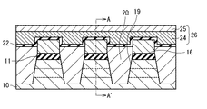
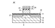
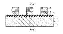
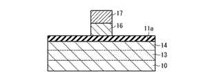
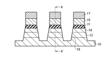
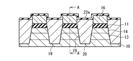
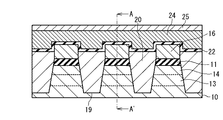
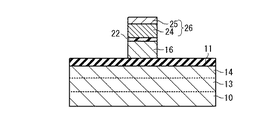
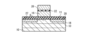
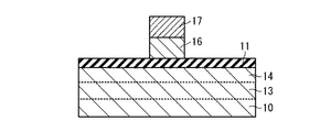
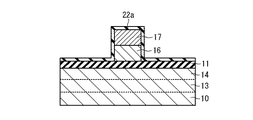
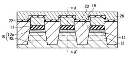
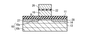
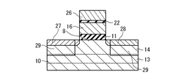
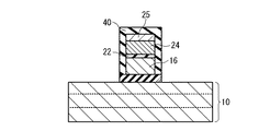
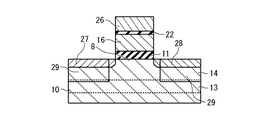
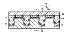
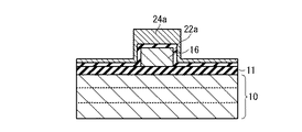
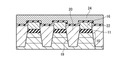
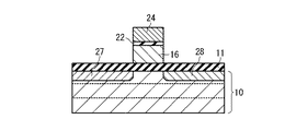
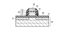
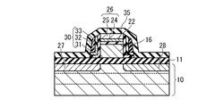
図1A及び図1Bは、本発明の不揮発性メモリの第1の実施の形態の構成を示す断面図である。ただし、図1Bは、図1AにおけるAA’断面図である。不揮発性メモリは、半導体基板10、ゲート絶縁層11、浮遊ゲート16、ポリシリコン層間絶縁層22、制御ゲート26及び素子分離絶縁部20を具備する。ここでは、半導体基板10の導電型がP型の場合について説明するが、N型の場合も同様に適用可能である。
1A and 1B are cross-sectional views showing the configuration of the first embodiment of the nonvolatile memory of the present invention. However, FIG. 1B is an AA ′ cross-sectional view in FIG. 1A. The nonvolatile memory includes a
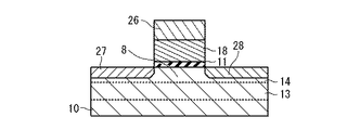
図1Bを参照して,半導体基板10は、N型不純物をドープしたディープNウエル13と、半導体基板10表面側のP型不純物をドープしたPウエル14を備える。Pウエル14には、N型のソース27及びドレイン28が半導体基板10表面に接するように設けられている。ソース27とドレイン28との間の領域は、不揮発性メモリのチャネル領域8(第1領域)である。両者の距離は、例えば、150nmである。
Referring to FIG. 1B, a
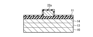
第1絶縁層としてのゲート絶縁層11は,チャネル領域8とソース27及びドレイン28の各々の少なくとも一部とを覆うように設けられている。材質は、例えば、酸化シリコンである。膜厚は、電荷がトンネルすることが可能な大きさであり、例えば、10nmである。
The
電荷蓄積層としての浮遊ゲート16は、チャネル領域8上のゲート絶縁層11を覆うように設けられている。材質は、例えば、ポリシリコンである。膜厚は、例えば、250nmである。半導体基板10に平行な平面の大きさは、例えば150nm×150nmである。
The floating
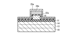
第2絶縁層としてのポリシリコン層間絶縁層22は、浮遊ゲート16を覆うように設けられている。材質は、例えば、酸窒化シリコンや、酸化シリコン/窒化シリコン/酸化シリコンの積層膜である。膜厚は、例えば、30nmである。
The polysilicon
制御ゲート26は、ポリシリコン層間絶縁層22を覆うように設けられている。制御ゲート26は、ポリシリコン層24及び金属層25を備える。ポリシリコン層24は、ポリシリコン層間絶縁層22を覆うように設けられている。膜厚は、例えば、100nmである。金属層25は、ポリシリコン層24を覆うように設けられている。金属層25はチャネル領域8に引張応力を及ぼし、チャネル領域8の圧縮応力を緩和する。金属層25の膜厚は例えば150nmである。その材質は、たとえば、タングステン、タンタル、モリブデン及びそれらの窒化物である。それらの組み合わせ(積層膜)でも良い。
The
金属層25は、その膜厚や、その膜中の材質を調整することにより、所望の引張応力とすることができる。また、上記タングステン等及びそれらの窒化物の成分の調整により、所望の引張応力とすることができる。例えば、タングステン等:他の導電性物質=90:10、などである。これにより、チャネル領域8の圧縮応力の大きさに対応して、その圧縮応力を緩和することができる。
The
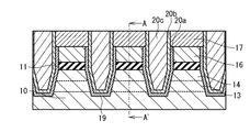
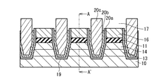
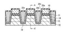
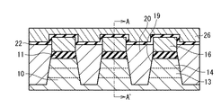
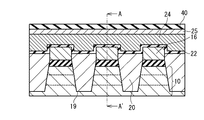
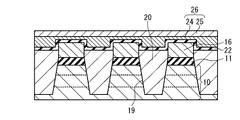
図1Aを参照して、半導体基板10には、隣接する素子同士を分離する素子分離溝19が設けられ、素子分離絶縁部20が満たされている。素子分離絶縁部20は、例えばSTI(Shallow Trench Isolation)である。その深さは、Nウエル13よりも深い。材質は、例えば、酸化シリコンである。
Referring to FIG. 1A, the
上記の構造を有する不揮発性メモリの特性について説明する。
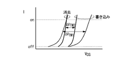
図34は、メモリセルの電圧と電流との関係を示すグラフである。縦軸はドレイン電流Iであり、onはオン電流に対応し、offがオフ電流に対応する。横軸は制御ゲートの電圧VCGである。
破線のグラフは、チャネル領域8の応力が高い場合を示す。実線のグラフは、チャネル領域8の応力が低い場合を示す。“消去”は、データが消去されている場合を示す。“書き込み”は、データが書き込まれている場合を示す。
The characteristics of the nonvolatile memory having the above structure will be described.
FIG. 34 is a graph showing the relationship between the voltage and current of the memory cell. The vertical axis represents the drain current I, on corresponds to the on current, and off corresponds to the off current. The horizontal axis represents the control gate voltage VCG .
A broken line graph indicates a case where the stress in the
この図において、チャネル領域8の応力が小さい場合(実線)の電圧VCGの閾値の変動ΔVTM2は、応力が大きい場合(破線)の電圧VCGの閾値の変動ΔVTM1に比較して小さくなる。データの書き換えに伴いチャネル領域8から浮遊ゲート16へ移動する電荷ΔQは、
ΔQ=CFG・ΔVTM
で表される。ここで、CFGは浮遊ゲート16とゲート絶縁層11とチャネル領域8とで形成される容量の大きさである。すなわち、応力を小さくするほど、閾値の変動ΔVTMが、例えばΔVTM1からΔVTM2へと小さくなる。そうすると、上式より、データの書き換え毎にゲート絶縁層11を介して出し入れする電荷量が小さくなる。それにより、ゲート酸化膜の劣化が抑制され、オン電流の劣化や、保持特性の劣化が抑制される。
In this figure, the variation [Delta] V TM2 threshold voltage V CG of the case the stress of the
ΔQ = C FG · ΔV TM
It is represented by Here, C FG is the size of the capacitance formed by the floating
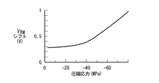
図35は、チャネル領域8の圧縮応力とゲート電圧の閾値の変動との関係を示すグラフである。縦軸はゲート電圧の閾値の変動であるVTMシフト(V)(上記のΔVTM)、横軸はチャネル領域8の圧縮応力(MPa)である。ただし、数字の符号であるマイナスは圧縮応力を示す。この図から、チャネル領域8の圧縮応力を小さくするほど、VTMシフト(ΔVTM)が小さく抑えられることが分かる。上記のような劣化の抑制等の効果を得るには、メモリセルの設計からVTMシフトを0.5V以下にすることが好ましい。その場合、チャネル領域8の圧縮応力を概ね50MPa以下にする必要があることが分かる。更に、VTMシフトを0.3V以下にすることがより好ましい。その場合、圧縮応力を概ね20MPa以下にする。
FIG. 35 is a graph showing the relationship between the compressive stress in the
一方、チャネル領域8の引張り応力が大きい場合、例えば、J.APPl.Phys.77、699−705(1995)、J.T.Yount、et al.に記載されるように、酸化シリコン/シリコン界面に存在する水素により終端された界面準位の結合が弱くなり、界面準位が生成しやすくなるという問題がある。トンネル膜/シリコン界面における界面準位の生成、回復は、フラッシュメモリではゲート電圧の閾値変動の原因となる。したがって、引張応力が大きい場合もフラッシュメモリの保持特性は劣化する。良好な保持特性を得るためのチャネル領域8の引張り応力上限値は必ずしも明らかではないが,少なくとも+50MPa以下の素子については良好な保持特性が得られることが分かっている。より好ましくは、+20MPaである。ただし、数字の符号のプラスは引張応力を示す。したがって、チャネル領域8が+50MPa以下の引張応力を有することは良好な保持特性を得るうえで好ましい。+20MPa以下の引張応力であることはより好ましい。
On the other hand, when the tensile stress of the
以上の結果から、チャネル領域8における応力Pは、−50MPa(圧縮)≦P≦+50MPa(引張)であることが好ましい。より好ましくは、−20MPa(圧縮)≦P≦+20MPa(引張)である。
From the above results, the stress P in the
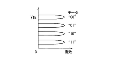
また、上記のようにΔVTMを小さくすることは、メモリセルの多値化にも効果がある。図36は、ゲート電圧の閾値の分布を示すグラフである。グラフの右側に示す“データ”は、記憶されるデータを示し、それに対応する閾値電圧VTMが縦軸に示されている。横軸は、その度数である。各データに対応する閾値電圧VTMは、そのVTMシフト(ΔVTM)が小さいほど、狭い範囲に分布する。この図では例として4種類のデータのいずれかを格納できるとしているが、VTMシフトを小さくするほど、より多くの種類のデータのいずれかを格納することが可能となる。 Further, reducing ΔV TM as described above is also effective in increasing the number of memory cells. FIG. 36 is a graph showing the distribution of threshold values of the gate voltage. “Data” shown on the right side of the graph indicates stored data, and the threshold voltage V TM corresponding to the data is shown on the vertical axis. The horizontal axis is the frequency. The threshold voltage V TM corresponding to each data is distributed in a narrower range as the V TM shift (ΔV TM ) is smaller. In this figure, one of four types of data can be stored as an example, but as the VTM shift is reduced, one of more types of data can be stored.
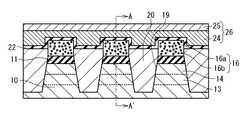
次に、本発明の不揮発性メモリの製造方法の第1の実施の形態について説明する。図2A及び図2B〜図11A及び図11Bは、本発明の不揮発性メモリの製造方法の実施の形態の各ステップを説明する断面図である。ただし、各図における図Aと図Bとの関係は、図1A及び図1Bとの関係(各図Bは各図Aの図1におけるAA’断面)と同じである。また説明には図1A及び図1Bも適宜用いる。 Next, a first embodiment of a method for manufacturing a nonvolatile memory according to the present invention will be described. 2A and 2B to FIG. 11A and FIG. 11B are cross-sectional views illustrating each step of the embodiment of the method for manufacturing a nonvolatile memory according to the present invention. However, the relationship between FIG. A and FIG. B in each drawing is the same as the relationship with FIG. 1A and FIG. 1B (each drawing B is an AA ′ cross section in FIG. 1 of each drawing A). In the description, FIGS. 1A and 1B are also used as appropriate.
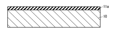
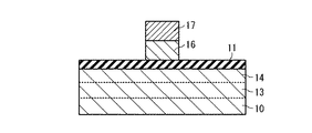
まず、図2A及び図2Bを参照して,表面を洗浄した半導体基板10を覆うように、熱酸化法で、ゲート絶縁膜11aを10nmの膜厚で形成する。
First, referring to FIGS. 2A and 2B, a
次に、図3A及び図3Bを参照して、ゲート絶縁膜11aを介して半導体基板10へN型不純物をイオン注入する。その後、熱処理により、ディープNウェル13を形成する。続いて、ゲート絶縁膜11aを介して半導体基板10へP型不純物をイオン注入する。その後、熱処理により、Pウェル14を形成する。
Next, referring to FIGS. 3A and 3B, N-type impurities are ion-implanted into the
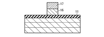
続いて、図4A及び図4Bを参照して、ゲート絶縁膜11aを覆うように、CVD(化学気相成長)法でポリシリコン膜を250nmの膜厚で形成する。そのポリシリコン膜上に、CVD法で窒化シリコン膜を150nmの膜厚で形成する。その後、フォトリソグラフィ及びエッチングの技術により、窒化シリコン膜及びポリシリコン膜をメモリセルの形状にパターンニングする。これより,窒化シリコン層17及び浮遊ゲート16が形成される。
4A and 4B, a polysilicon film having a thickness of 250 nm is formed by CVD (chemical vapor deposition) so as to cover the
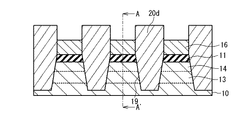
その後、図5Aを参照して、窒化シリコン層17及び浮遊ゲート16に対して、フォトリソグラフィ及びエッチングの技術により、自己整合的に素子分離溝(トレンチ)19を形成する。その深さは、ディープNウエル13よりも深くする。ゲート絶縁膜11aは、ゲート絶縁層11になる。ただし、図5Bを参照して、図5B方向については、素子分離溝を形成しない。
Thereafter, referring to FIG. 5A, element isolation trenches (trench) 19 are formed in a self-aligned manner with respect to
次に、図6A及び図6Bを参照して、素子分離溝19を埋め、窒化シリコン層17及び浮遊ゲート16の周辺及び上部を覆うように高密度プラズマCVD法により、酸化シリコン層20dを形成する。そして、窒化シリコン17の表面が露出し、酸化シリコン層20dの表面が平坦になるようにCMP(化学機械研磨)法で、酸化シリコン層20dを研磨する。
Next, referring to FIGS. 6A and 6B, a
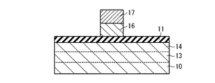
続いて、図7A及び図7Bを参照して、浮遊ゲート16上の窒化シリコン層17をウエットエッチングの技術により除去する。
Subsequently, referring to FIGS. 7A and 7B, the
次に、図8A及び図8Bを参照して、異方性エッチングの技術により、酸化シリコン層20dを浮遊ゲート16の高さよりも低くし,素子分離絶縁部20とする。そして、素子分離絶縁部20、浮遊ゲート16及びゲート絶縁層11を覆うように、CVD法で、酸窒化シリコン膜22aを30nmの膜厚で形成する。
Next, referring to FIGS. 8A and 8B, the
更に、図9A及び図9Bを参照して、酸窒化シリコン膜22aを覆うように、CVD法で、ポリシリコン膜24aを100nmの膜厚で形成する。さらにポリシリコン膜を覆うように、マグネトロンスパッタ法でタングステン膜25aを形成する。このタングステン膜25aは半導体基板10に引張応力を印加する。この応力を用いて、チャネル領域の応力を制御することができる。堆積速度や、スパッタ時の基板温度、膜厚を変化させ応力値を所望の値となるように制御する。
Furthermore, referring to FIGS. 9A and 9B, a
その後、図10A及び図10Bを参照して、フォトリソグラフィ及びエッチングの技術により、酸窒化シリコン膜22a、ポリシリコン膜24a及びタングステン膜25aをパターンニングして、ポリシリコン層間絶縁層22、ポリシリコン層24、及び金属層25を形成する。
Thereafter, referring to FIGS. 10A and 10B, the
図11A及び図11Bを参照して、ポリシリコン層24をマスクとして、N型不純物のイオン注入を行う。その後、熱処理により、ソース27及びドレイン28を形成する。
Referring to FIGS. 11A and 11B, N-type impurity ions are implanted using
上記製造方法により、図1A及び図1Bに示すチャネル領域8の応力の小さい不揮発性メモリを製造することができる。
With the above manufacturing method, a nonvolatile memory with a small stress in the
本発明により、チャネル領域の応力を緩和することができ、チャネル領域での電子の移動度を向上させることができる。そのため、メモリセルのオン/オフ比が向上し、書き換え毎に浮遊ゲートに出し入れする電荷量を小さくすることができる。そして、ゲート絶縁膜(トンネル酸化膜)の劣化を低減することが可能となる。加えて、ゲート絶縁膜(トンネル酸化膜)とチャネル領域との界面の応力を緩和することで、書き換え動作により生成される界面準位の増加が抑制される。それにより、オン電流の劣化を抑えることができる。それにより、不揮発性メモリにおける書き込み消去の書き換え動作の繰り返しよるオン電流の低下や、保持特性の劣化が抑制できる。 According to the present invention, stress in the channel region can be relieved and electron mobility in the channel region can be improved. As a result, the on / off ratio of the memory cell is improved, and the amount of charge withdrawn into and out of the floating gate for each rewrite can be reduced. And it becomes possible to reduce deterioration of a gate insulating film (tunnel oxide film). In addition, by relaxing the stress at the interface between the gate insulating film (tunnel oxide film) and the channel region, an increase in the interface state generated by the rewriting operation is suppressed. Thereby, deterioration of on-current can be suppressed. As a result, it is possible to suppress a decrease in on-state current and deterioration of retention characteristics due to repetitive write / erase rewrite operations in the nonvolatile memory.
(第2の実施の形態)
以下、本発明の不揮発性メモリの第2の実施の形態に関して、添付図面を参照して説明する。
(Second Embodiment)
Hereinafter, a second embodiment of the nonvolatile memory according to the present invention will be described with reference to the accompanying drawings.
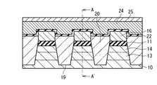
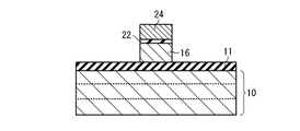
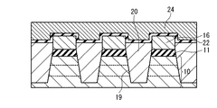
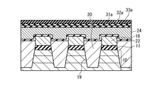
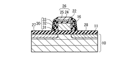
図12A及び図12Bは、本発明の不揮発性メモリの第2の実施の形態の構成を示す断面図である。ただし、図12Bは、図12AにおけるAA’断面図である。不揮発性メモリは、半導体基板10、ゲート絶縁層11、浮遊ゲート16、ポリシリコン層間絶縁層22、制御ゲート26及び素子分離絶縁部20を具備する。ここでは、半導体基板10の導電型がP型の場合について説明するが,N型の場合も同様に適用可能である。
12A and 12B are cross-sectional views showing the configuration of the second embodiment of the nonvolatile memory of the present invention. However, FIG. 12B is an AA ′ cross-sectional view in FIG. 12A. The nonvolatile memory includes a
図12Bを参照して、半導体基板10は、N型不純物をドープしたディープNウエル13と、半導体基板10表面側のP型不純物をドープしたPウエル14を備える。Pウエル14には、N型のソース27及びドレイン28が半導体基板10表面に接するように設けられている。ソース27とドレイン28との間の領域は、不揮発性メモリのチャネル領域8(第1領域)である。両者の距離は、例えば、150nmである。
Referring to FIG. 12B, the
第1絶縁層としてのゲート絶縁層11は、チャネル領域8とソース27及びドレイン28の各々の少なくとも一部とを覆うように設けられている。材質は、例えば、酸化シリコンである。膜厚は、電荷がトンネルすることが可能な大きさであり、例えば、10nmである。
The
電荷蓄積層としての浮遊ゲート16は、チャネル領域8上のゲート絶縁層11を覆うように設けられている。材質は、例えば,ポリシリコンである。膜厚は、例えば、250nmである。半導体基板10に平行な平面の大きさは、例えば150nm×150nmである。
The floating
第2絶縁層としてのポリシリコン層間絶縁層22は、浮遊ゲート16を覆うように設けられている。材質は、例えば、酸窒化シリコンや、酸化シリコン/窒化シリコン/酸化シリコンの積層膜である。膜厚は、例えば、30nmである。
The polysilicon
制御ゲート26は、ポリシリコン層間絶縁層22を覆うように設けられている。材質は、例えば、多結晶シリコンである。膜厚は、例えば、200nmである。
The
図12Aを参照して、半導体基板10には、隣接する素子同士を分離する素子分離溝19が設けられ、素子分離絶縁部20が満たされている。素子分離絶縁部20は、素子分離溝19に接する側から順に、酸化シリコン20a、窒化シリコン20b、酸化シリコン20cの層状構造をもつSTI(Shallow Trench Isolation)である。その深さは、ディープNウエル13よりも深く設ける。酸化シリコン20a、窒化シリコン20bの厚さは、例えば10nm、3nmである。この層状構造をもつSTIによりチャネル領域の応力を制御することができる。
Referring to FIG. 12A, the
層状構造をもつSTIは、その各膜の膜厚の組み合わせ及び成膜条件、素子分離溝19の深さを調整することにより、チャネル領域8に与える応力を小さくすることができる。また、素子分離絶縁部20に用いる膜の材質(成分)の調整により、チャネル領域8に与える応力を小さくすることができる。
The STI having a layered structure can reduce the stress applied to the
図34〜図36については、第1の実施の形態と同様であるので、その説明を省略する。 34 to 36 are the same as those in the first embodiment, and thus the description thereof is omitted.
次に、本発明の不揮発性メモリの製造方法の第2の実施の形態について説明する。図2A及び図2B〜図5A及び図5B、図19A及び図19B〜図21A及び図21B、図9A及び図9B〜図11A及び図11Bは、本発明の不揮発性メモリの製造方法の実施の形態の各ステップを説明する断面図である。ただし、各図における図Aと図Bとの関係は、図12A及び図12Bとの関係(各図Bは各図Aの図12におけるAA’断面)と同じである。また説明には図12A及び図12Bも適宜用いる。 Next, a second embodiment of the method for manufacturing a nonvolatile memory according to the present invention will be described. 2A and 2B to 5A and 5B, FIG. 19A and FIG. 19B to FIG. 21A and FIG. 21B, and FIG. 9A and FIG. 9B to FIG. 11A and FIG. It is sectional drawing explaining each of these steps. However, the relationship between FIG. A and FIG. B in each drawing is the same as the relationship with FIG. 12A and FIG. 12B (each drawing B is an AA ′ cross section in FIG. 12 of each drawing A). In the description, FIGS. 12A and 12B are also used as appropriate.
まず、不揮発性メモリの製造方法の第1の実施の形態に基づき、図2A及び図2B〜図5A及び図5Bに示される素子分離溝19の形成まで行う。
First, based on the first embodiment of the manufacturing method of the nonvolatile memory, the process up to the formation of the
次に、図13A及び図13Bを参照して、素子分離溝19の内壁及び浮遊ゲート16の外壁を熱酸化法で酸化して、酸化シリコン層20aを形成する。厚さは、例えば10nmである。続いて、プラズマCVD法で窒化シリコン膜20bを形成する。厚さは、例えば3nmである。さらに、高密度プラズマCVD法で酸化シリコン膜20cを、素子分離溝19を埋めるように形成する。そして、窒化シリコン膜17の表面が露出するまで、窒化シリコン膜20b及び酸化シリコン膜20cをCMPで研磨する。このような層状構造を持つSTIは通常のSTIに比べ、チャネル領域に与える圧縮応力が小さい。したがって、良好な保持特性を得ることができる。チャネル領域に与える応力の大きさは窒化シリコン膜20bの厚さや、酸化シリコン層20aの酸化条件により制御することができる。
Next, referring to FIGS. 13A and 13B, the inner wall of
続いて、図14A及び図14Bを参照して、ウエットエッチングにより、浮遊ゲート16上の窒化シリコン層17及び窒化シリコン層20bの一部を取り除く。
Subsequently, referring to FIGS. 14A and 14B, the
次に、図15A及び図15Bを参照して、異方性エッチングの技術により、酸化シリコン層20a及び酸化シリコン膜20cを窒化シリコン層20bの高さに合わせ、素子分離絶縁部20とする。そして、素子分離絶縁部20、浮遊ゲート16及びゲート絶縁層11を覆うように、CVD法で、酸窒化シリコン膜22aを形成する。膜厚は、例えば30nmである。
Next, referring to FIG. 15A and FIG. 15B, the
その後、上記の不揮発性メモリの製造方法の第1の実施の形態における図9A及び図9B〜図11A及び図11Bで説明したステップ(工程)に基づき、上部構造およびソース27とドレイン28を形成する。ただし、上部構造を形成する際、金属膜25を形成するステップは必ずしも必要ではない。また、そのステップは、シリコンと金属との化合物薄膜を形成するステップであっても良い。
Thereafter, the upper structure and the
上記製造方法により、図12A及び図12Bに示されるチャネル領域8の応力の小さい不揮発性メモリを製造することができる。
By the manufacturing method described above, a nonvolatile memory having a small stress in the
本実施の形態においても、第1の実施の形態で説明したものと同様の効果を得ることができる。 Also in this embodiment, the same effects as those described in the first embodiment can be obtained.
(第3の実施の形態)
以下、本発明の不揮発性メモリの第3の実施の形態に関して、添付図面を参照して説明する。
(Third embodiment)
Hereinafter, a third embodiment of the nonvolatile memory of the present invention will be described with reference to the accompanying drawings.
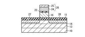
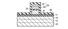
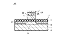
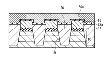
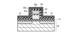
図16A及び図16Bは、本発明の不揮発性メモリの第3の実施の形態の構成を示す断面図である。ただし、図16Bは、図16AにおけるAA’断面図である。不揮発性メモリは、半導体基板10、ゲート絶縁層11、浮遊ゲート16、層間絶縁層22、制御ゲート26及び素子分離絶縁部20を具備する。ここでは、半導体基板10がP型の場合について説明するが、N型の場合も同様に適用可能である。
16A and 16B are cross-sectional views showing the configuration of the third embodiment of the nonvolatile memory of the present invention. However, FIG. 16B is a cross-sectional view along AA ′ in FIG. 16A. The nonvolatile memory includes a
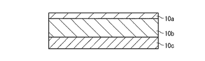
図16Bを参照して、半導体基板10は、その表面側から順にシリコン層10a、シリコンゲルマニウム層10bの層構造を含む。不揮発性メモリが作られる前のシリコン層10aはシリコンゲルマニウム層10bから引張応力を受けており、不揮発性メモリが作られることにより生じる圧縮応力が打ち消されることになる。これによりチャネル領域8の応力を制御することができる。さらに、半導体基板10はN型不純物をドープしたディープNウエル13と、半導体基板10表面側のP型不純物をドープしたPウエル14を備える。Pウエル14には、N型のソース27及びドレイン28が半導体基板10表面に接するように設けられている。ソース27とドレイン28との間の領域は、不揮発性メモリのチャネル領域8(第1領域)である。両者の距離は、例えば、150nmである。
Referring to FIG. 16B, the
層構造をもつ半導体基板10は、シリコンゲルマニウム層10b及びシリコン層10aの膜厚の組み合わせ及び成膜条件を調整することにより、チャネル領域8に与える応力を調整することができる。
The
第1絶縁層としてのゲート絶縁層11は、チャネル領域8とソース27及びドレイン28の各々の少なくとも一部とを覆うように設けられている。材質は、例えば、酸化シリコンである。膜厚は、電荷がトンネルすることが可能な大きさであり、例えば、10nmである。
The
電荷蓄積層としての浮遊ゲート16は、チャネル領域8上のゲート絶縁層11を覆うように設けられている。材質は、例えば、ポリシリコンである。膜厚は、例えば、250nmである。半導体基板10に平行な平面の大きさは、例えば150nm×150nmである。
The floating
第2絶縁層としての層間絶縁層22は、浮遊ゲート16を覆うように設けられている。材質は、例えば、酸窒化シリコンや、酸化シリコン/窒化シリコン/酸化シリコンの積層膜である。膜厚は、例えば,30nmである。
The interlayer insulating
制御ゲート26は、層間絶縁層22を覆うように設けられている。材質は例えばポリシリコンである。膜厚は、例えば、200nmである。
The
図16Aを参照して、半導体基板10には、隣接する素子同士を分離する素子分離溝19が設けられ、素子分離絶縁部20が満たされている。素子分離絶縁部20は、例えばSTI(Shallow Trench Isolation)である。その深さは、ディープNウエル13よりも深く設ける。材質は、例えば、酸化シリコンである。
Referring to FIG. 16A, the
図34〜図36については、第1の実施の形態と同様であるので、その説明を省略する。 34 to 36 are the same as those in the first embodiment, and thus the description thereof is omitted.
次に、本発明の不揮発性メモリの製造方法の第3の実施の形態について説明する。図17A及び図17B、図2A及び図2B〜図11A及び図11Bは、本発明の不揮発性メモリの製造方法の実施の形態の各ステップを説明する断面図である。ただし、各図における図Aと図Bとの関係は、図16A及び図16Bとの関係(各図Bは各図Aの図16におけるAA’断面)と同じである。また説明には図16A及び図16Bも適宜用いる。 Next, a third embodiment of the method for manufacturing a nonvolatile memory according to the present invention will be described. 17A and 17B, FIG. 2A and FIG. 2B to FIG. 11A and FIG. 11B are cross-sectional views illustrating each step of the embodiment of the method for manufacturing a nonvolatile memory according to the present invention. However, the relationship between FIG. A and FIG. B in each drawing is the same as the relationship with FIG. 16A and FIG. 16B (each drawing B is an AA ′ cross section in FIG. 16 of each drawing A). In addition, FIG. 16A and FIG.
図17A及び図17Bを参照して、まず表面を洗浄したシリコン基板10c上にCVD法によりシリコンゲルマニウム膜をシリコンゲルマニウム層10bとしてエピタキシャル成長させる。このとき、シリコンゲルマニウム膜の膜厚は、シリコン基板10cとの間に発生する応力が緩和するのに十分で、且つ、この応力緩和に伴い生じる結晶欠陥が、デバイス製造に支障のない密度にまで減少する膜厚である。その後CVD法によりシリコン膜をシリコン層10aとしてエピタキシャル成長させる。このシリコン膜にはシリコンゲルマニウム膜との格子定数の差から生じる引張応力が印加されている。これによりチャネル領域8の応力を制御することができる。
Referring to FIGS. 17A and 17B, first, a silicon germanium film is epitaxially grown as a
その後、上記の不揮発性メモリの製造方法の第1の実施の形態における図2A及び図2B〜図11A及び図11Bで説明したステップに基づき、図17A及び図17Bに示された基板上に不揮発性メモリを形成する。その際、金属膜25を形成するステップは必ずしも必要ではない。また、そのステップは、シリコンと金属との化合物薄膜を形成するステップであっても良い。
Then, based on the steps described in FIGS. 2A and 2B to 11A and 11B in the first embodiment of the method for manufacturing the nonvolatile memory described above, the nonvolatile memory is formed on the substrate shown in FIGS. 17A and 17B. Form a memory. At this time, the step of forming the
上記製造方法により、図16A及び図16Bに示されるチャネル領域8の応力の小さい不揮発性メモリを製造することができる。
With the above manufacturing method, a nonvolatile memory with a small stress in the
本実施の形態においても、第1の実施の形態で説明したものと同様の効果を得ることができる。 Also in this embodiment, the same effects as those described in the first embodiment can be obtained.
(第4の実施の形態)
以下、本発明の不揮発性メモリの第4の実施の形態に関して、添付図面を参照して説明する。
(Fourth embodiment)
Hereinafter, a fourth embodiment of the nonvolatile memory of the present invention will be described with reference to the accompanying drawings.
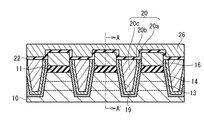
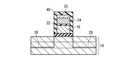
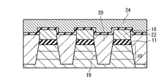
図18A及び図18Bは、本発明の不揮発性メモリの第4の実施の形態の構成を示す断面図である。ただし、図18Bは、図18AにおけるAA’断面図である。不揮発性メモリは、シリコン基板10、ゲート絶縁層11、浮遊ゲート16、層間絶縁層22、制御ゲート26及び素子分離絶縁部20を具備する。ここでは、シリコン基板10がP型の場合について説明するが、N型の場合も同様に適用可能である。
18A and 18B are cross-sectional views showing the configuration of the fourth embodiment of the nonvolatile memory of the present invention. However, FIG. 18B is an AA ′ sectional view in FIG. 18A. The nonvolatile memory includes a
図18Bを参照して、シリコン基板10は、N型不純物をドープしたディープNウエル13と、半導体基板10表面側のP型不純物をドープしたPウエル14を備える。Pウエル14には、N型のソース27及びドレイン28が半導体基板10表面に接するように設けられている。ソース27とドレイン28との間の領域は、不揮発性メモリのチャネル領域8(第1領域)である。両者の距離は、例えば、150nmである。領域29は半導体基板10をエッチングした後、炭素を添加したシリコンをエピタキシャル成長させた領域である。領域29は、ソース27とドレイン28は領域29の一部を含むように設けられている。この構造をとることで、チャネル領域8には引張応力が印加される。この応力は、チャネル領域8のシリコンと領域29の炭素を添加したシリコンとの間の格子定数の差によって生じる。その応力の大きさは炭素の添加量や、領域29とチャネル8との位置関係、深さを変えることで調整することができる。それにより、その応力を使って、チャネル領域8の応力を制御することができる。
Referring to FIG. 18B,
第1絶縁層としてのゲート絶縁層11は、チャネル領域8とソース27及びドレイン28の各々の少なくとも一部とを覆うように設けられている。材質は、例えば、酸化シリコンである。膜厚は,電荷がトンネルすることが可能な大きさであり、例えば、10nmである。
The
電荷蓄積層としての浮遊ゲート16は、チャネル領域8上のゲート絶縁層11を覆うように設けられている。材質は、例えば、ポリシリコンである。膜厚は、例えば、250nmである。半導体基板10に平行な平面の大きさは、例えば150nm×150nmである。
The floating
第2絶縁層としてのポリシリコン層間絶縁層22は、浮遊ゲート16を覆うように設けられている。材質は、例えば、酸窒化シリコンや、酸化シリコン/窒化シリコン/酸化シリコンの積層膜である。膜厚は、例えば、30nmである。
The polysilicon
制御ゲート26は、層間絶縁層22を覆うように設けられている。材質は例えばポリシリコンである。膜厚は、例えば、200nmである。
The
図18Aを参照して、半導体基板10には、隣接する素子同士を分離する素子分離溝19が設けられ、素子分離絶縁部20が満たされている。素子分離絶縁部20は、例えばSTI(Shallow Trench Isolation)である。その深さは、ディープNウエル13よりも深く設ける。材質は、例えば、酸化シリコンである。
Referring to FIG. 18A, the
図34〜図36については、第1の実施の形態と同様であるので、その説明を省略する。 34 to 36 are the same as those in the first embodiment, and thus the description thereof is omitted.
次に、本発明の不揮発性メモリの製造方法の第4の実施の形態について説明する。図2A及び図2B〜図10A及び図10B、図19A及び図19B〜図22A及び図22Bは、本発明の不揮発性メモリの製造方法の実施の形態の各ステップを説明する断面図である。ただし、各図における図Aと図Bとの関係は、図18A及び図18Bとの関係(各図Bは各図Aの図18におけるAA’断面)と同じである。また説明には図18A及び図18Bも適宜用いる。 Next, a fourth embodiment of the method for manufacturing a nonvolatile memory according to the present invention will be described. 2A and 2B to FIG. 10A and FIG. 10B, FIG. 19A and FIG. 19B to FIG. 22A and FIG. 22B are cross-sectional views illustrating each step of the embodiment of the method for manufacturing a nonvolatile memory according to the present invention. However, the relationship between FIG. A and FIG. B in each drawing is the same as the relationship with FIG. 18A and FIG. 18B (each drawing B is an AA ′ cross section in FIG. 18 of each drawing A). 18A and 18B are also used as appropriate for the description.
まず、不揮発性メモリの製造方法の第1の実施の形態に基づき、図2A及び図2B〜図10A及び図10Bに示される制御ゲート26の形成までを行う。この際、金属膜25を形成するステップは必ずしも必要ではない。また、このステップがシリコンと金属との化合物薄膜を形成するステップであっても良い。
First, based on the first embodiment of the manufacturing method of the nonvolatile memory, the process up to the formation of the
次に、図19A及び図19Bを参照して、浮遊ゲート16、層間絶縁層22、制御ゲート26及びゲート絶縁層11を覆うようにCVD法により酸化シリコン膜40を形成する。
Next, referring to FIGS. 19A and 19B, a
続いて、図20A及び図20Bを参照して、フォトリソグラフィ及びエッチングの技術により、酸化シリコン膜40及びゲート絶縁膜11をパターンニングする。
Subsequently, referring to FIGS. 20A and 20B, the
その後、図21A及び図21Bを参照して、酸化シリコン膜40をマスクとして半導体基板10をドライエッチングによりエッチングする。さらに、エッチングされた半導体基板表面を洗浄した後、選択的エピタキシャル成長の技術により半導体基板のエッチングされた領域にのみ,炭素が添加されたシリコン膜29を形成する。この炭素が添加されたシリコン膜29と半導体基板10との間の格子定数の差により、チャネル領域には引張応力が印加される。この応力によりチャネル領域の応力を制御することが可能となる。チャネル領域に印加される引張り応力の大きさは、添加される炭素の量により制御することができる。
21A and 21B, the
次に、図22A及び図22Bを参照して、酸化シリコン膜をエッチングにより除去する。続いて、制御ゲート26をマスクとして、N型不純物のイオン注入を行う。その後、熱処理により、ソース27及びドレイン28を形成する。
Next, referring to FIGS. 22A and 22B, the silicon oxide film is removed by etching. Subsequently, ion implantation of N-type impurities is performed using the
上記製造方法により、図18A及び図18Bに示されるチャネル領域8の応力の小さい不揮発性メモリを製造することができる。
By the above manufacturing method, it is possible to manufacture a nonvolatile memory with a small stress in the
本実施の形態においても、第1の実施の形態で説明したものと同様の効果を得ることができる。 Also in this embodiment, the same effects as those described in the first embodiment can be obtained.
(第5の実施の形態)
以下、本発明の不揮発性メモリの第5の実施の形態に関して、添付図面を参照して説明する。
(Fifth embodiment)
Hereinafter, a fifth embodiment of the nonvolatile memory of the present invention will be described with reference to the accompanying drawings.
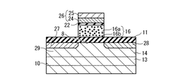
図23A及び図23Bは、本発明の不揮発性メモリの第5の実施の形態の構成を示す断面図である。ただし、図23Bは、図23AにおけるAA’断面図である。不揮発性メモリは、シリコン基板10、ゲート絶縁層11、電荷蓄積絶縁層16、層間絶縁層22、制御ゲート26及び素子分離絶縁部20を具備する。ここでは,半導体基板10の導電型がP型の場合について説明するが、N型の場合も同様に適用可能である。
23A and 23B are cross-sectional views showing the configuration of the fifth embodiment of the nonvolatile memory of the present invention. However, FIG. 23B is an AA ′ sectional view in FIG. 23A. The nonvolatile memory includes a
図23Bを参照して、半導体基板10は、N型不純物をドープしたディープNウエル13と、半導体基板10表面側のP型不純物をドープしたPウエル14を備える。Pウエル14には、N型のソース27及びドレイン28が半導体基板10表面に接するように設けられている。ソース27とドレイン28との間の領域は、不揮発性メモリのチャネル領域8(第1領域)である。両者の距離は、例えば、150nmである。
Referring to FIG. 23B, the
ゲート絶縁層11は、チャネル領域8とソース27及びドレイン28の各々の少なくとも一部とを覆うように設けられている。材質は、例えば、酸化シリコンである。膜厚は、電荷がトンネルすることが可能な大きさであり、例えば、1.5nmである。
The
電荷蓄積絶縁層16は、チャネル領域8上のゲート絶縁層11上に設けられている。材質は,シリコン微粒子16bを含んだ酸化シリコン膜16aである。酸化シリコン膜16aの膜厚は、例えば、250nmである。シリコン微粒子16bの粒径は例えば5nmである。半導体基板10に平行な平面の大きさは,例えば150nm×150nmである。
The charge
層間絶縁層22は,電荷蓄積絶縁層を覆うように設けられている。材質は、例えば、酸化シリコンである。膜厚は、例えば7nmである。
The interlayer insulating
制御ゲート26は、層間絶縁層22を覆うように設けられている。制御ゲート26は、金属層25及びポリシリコン層24を備える。ポリシリコン層24は、ポリシリコン層間絶縁層22を覆うように設けられている。膜厚は、例えば、100nmである。金属層25は、ポリシリコン層24を覆うように設けられている。金属層25はチャネル領域8に引張応力を及ぼし、チャネル領域8の圧縮応力を緩和する。金属層26Aの膜厚は、例えば150nmである。その材質は、たとえば、タングステン、タンタル、モリブデンおよびそれらの窒化物である。
The
金属層25は、その膜厚や、その膜中の材質を調整することにより、所望の引張応力とすることができる。また、上記タングステン等及びそれらの窒化物の成分調整により、所望の引張応力とすることができる。これにより、チャネル領域8の圧縮応力の大きさに対応して、その圧縮応力を緩和することができる。
The
図23Aを参照して、半導体基板10には、隣接する素子同士を分離する素子分離溝19が設けられ,素子分離絶縁部20が満たされている。素子分離絶縁部20は、例えばSTI(Shallow Trench Isolation)である。その深さは、Nウエル13よりも深く設ける。材質は、例えば、酸化シリコンである。
Referring to FIG. 23A, the
図34〜図36については、第1の実施の形態と同様であるので、その説明を省略する。 34 to 36 are the same as those in the first embodiment, and thus the description thereof is omitted.
本発明の不揮発性メモリの製造方法の第5の実施の形態については、電荷蓄積絶縁層16の材質が異なるほかは、第1の実施の形態と同様であるのでその説明を省略する。ただし、電荷蓄積絶縁層16は、シリコン微粒子を分散された酸化シリコンのスラリーを塗布、焼成して形成することが出来る。
Since the fifth embodiment of the method for manufacturing a nonvolatile memory according to the present invention is the same as the first embodiment except that the material of the charge
本実施の形態においても、第1の実施の形態で説明したものと同様の効果を得ることができる。 Also in this embodiment, the same effects as those described in the first embodiment can be obtained.
(第6の実施の形態)
以下、本発明の不揮発性メモリの第6の実施の形態に関して、添付図面を参照して説明する。
(Sixth embodiment)
Hereinafter, a sixth embodiment of the nonvolatile memory of the present invention will be described with reference to the accompanying drawings.
図24A及び図24Bは、本発明の不揮発性メモリの第6の実施の形態の構成を示す断面図である。ただし、図24Bは、図24AにおけるAA’断面図である。不揮発性メモリは、シリコン基板10、ゲート絶縁層11、電荷蓄積絶縁層16、層間絶縁層22、制御ゲート26及び素子分離絶縁部20を具備する。ここでは,半導体基板10の導電型がP型の場合について説明するが、N型の場合も同様に適用可能である。
24A and 24B are cross-sectional views showing the configuration of the sixth embodiment of the nonvolatile memory of the present invention. However, FIG. 24B is a cross-sectional view along AA ′ in FIG. 24A. The nonvolatile memory includes a
図24Bを参照して、半導体基板10は、N型不純物をドープしたディープNウエル13と、半導体基板10表面側のP型不純物をドープしたPウエル14を備える。Pウエル14には、N型のソース27及びドレイン28が半導体基板10表面に接するように設けられている。ソース27とドレイン28との間の領域は、不揮発性メモリのチャネル領域8(第1領域)である。両者の距離は、例えば、150nmである。
Referring to FIG. 24B, the
ゲート絶縁層11は、チャネル領域8とソース27及びドレイン28の各々の少なくとも一部とを覆うように設けられている。材質は、例えば、酸化シリコンである。膜厚は、電荷がトンネルすることが可能な大きさであり、例えば、7nmである。
The
電荷蓄積絶縁層16は、チャネル領域8上のゲート絶縁層11上に設けられている。材質は、例えば、窒化シリコン、酸化アルミニウム、酸窒化アルミニウム、酸化ハフニウム、酸窒化ハフニウム、酸窒化シリコンハフニウム、酸化ジルコニウム、酸窒化ジルコニウム、酸窒化シリコンジルコニウムのいずれかである。これらの材料により形成される電荷蓄積層16は、電荷捕獲中心を含有する。膜厚は、例えば、10nmである。半導体基板10に平行な平面の大きさは、例えば150nm×150nmである。
The charge
層間絶縁層22は、電荷蓄積絶縁層16の上に設けられている。材質は、例えば、酸化シリコンである。膜厚は例えば7nmである。
The interlayer insulating
制御ゲート26は、層間絶縁層22を覆うように設けられている。制御ゲート26は、金属層25及びポリシリコン層24を備える。ポリシリコン層24は、ポリシリコン層間絶縁層22を覆うように設けられている。膜厚は、例えば、100nmである。金属層25は、ポリシリコン層26Aを覆うように設けられている。金属層25はチャネル領域8に引張応力を及ぼし、チャネル領域8の圧縮応力を緩和する。金属層25の膜厚は例えば150nmである。その材質は、たとえば、タングステン、タンタル、モリブデンおよびそれらの窒化物、それらの組み合わせ(積層)である。
The
図24Aを参照して、半導体基板10には、隣接する素子同士を分離する素子分離溝19が設けられ、素子分離絶縁部20が満たされている。素子分離絶縁部20は、例えばSTI(Shallow Trench Isolation)である。その深さは、Nウエル13よりも深く設ける。材質は、例えば、酸化シリコンである。
Referring to FIG. 24A, the
図34〜図36については、第1の実施の形態と同様であるので、その説明を省略する。 34 to 36 are the same as those in the first embodiment, and thus the description thereof is omitted.
本発明の不揮発性メモリの製造方法の第6の実施の形態については、電荷蓄積絶縁層16の材質が異なるほかは、第1の実施の形態と同様であるのでその説明を省略する。
Since the sixth embodiment of the method for manufacturing a nonvolatile memory according to the present invention is the same as the first embodiment except that the material of the charge
本実施の形態においても、第1の実施の形態で説明したものと同様の効果を得ることができる。 Also in this embodiment, the same effects as those described in the first embodiment can be obtained.
(第7の実施の形態)
以下、本発明の不揮発性メモリの第7の実施の形態に関して、添付図面を参照して説明する。
(Seventh embodiment)
Hereinafter, a seventh embodiment of the nonvolatile memory of the present invention will be described with reference to the accompanying drawings.
図25A及び図25Bは、本発明の不揮発性メモリの第7の実施の形態の構成を示す断面図である。ただし、図25Bは、図25AにおけるAA’断面図である。不揮発性メモリは、半導体基板10、ゲート絶縁層11、強誘電体層18、制御ゲート26及び素子分離絶縁部20を具備する。ここでは、半導体基板10の導電型がP型の場合について説明するが、N型の場合も同様に適用可能である。強誘電体層18はゲート絶縁層11側から順に金属、強誘電体の積層構造をとる薄膜であっても良い。
25A and 25B are cross-sectional views showing the configuration of the seventh embodiment of the nonvolatile memory of the present invention. However, FIG. 25B is a cross-sectional view along AA ′ in FIG. 25A. The nonvolatile memory includes a
図25Bを参照して、半導体基板10は、N型不純物をドープしたディープNウエル13と、半導体基板10表面側のP型不純物をドープしたPウエル14を備える。Pウエル14には、N型のソース27及びドレイン28が半導体基板10表面に接するように設けられている。ソース27とドレイン28との間の領域は、不揮発性メモリのチャネル領域8(第1領域)である。両者の距離は、例えば、150nmである。
Referring to FIG. 25B, the
第1絶縁層としてのゲート絶縁層11は、チャネル領域8とソース27及びドレイン28の各々の少なくとも一部とを覆うように設けられている。材質は、例えば、酸化ハフニウムである。膜厚は、例えば、8nmである。
The
電荷蓄積層としての強誘電体層18は、チャネル領域8上のゲート絶縁層11の上に設けられている。材質は、例えば、タンタル酸ビスマス酸ストロンチウムである。膜厚は、例えば、250nmである。半導体基板10に平行な平面の大きさは、例えば150nm×150nmである。ゲート絶縁層11と強誘電体層18との間に金属層(図示されず)を有していても良い。
A
制御ゲート26は、強誘電体層16の上に設けられている。材質は例えばルテニウムである。膜厚は例えば100nmである。
The
図25Aを参照して,半導体基板10には、隣接する素子同士を分離する素子分離溝19が設けられ、素子分離絶縁部20が満たされている。素子分離絶縁部20は、酸化シリコン20a、窒化シリコン20b、酸化シリコン20cの層状構造をもつSTI(Shallow Trench Isolation)である。その深さは、ディープNウエル13よりも深く設ける。酸化シリコン20a、窒化シリコン20bの厚さは例えば10nm、3nmである。この層状構造をもつSTIにより、第2の実施の形態と同様にチャネル領域の応力を制御することができる。
Referring to FIG. 25A, the
図34〜図36については、第1の実施の形態と同様であるので、その説明を省略する。 34 to 36 are the same as those in the first embodiment, and thus the description thereof is omitted.
本発明の不揮発性メモリの製造方法の第7の実施の形態については、層間絶縁層22を設けないほかは、第2の実施の形態と同様であるのでその説明を省略する。
Since the seventh embodiment of the method for manufacturing a nonvolatile memory according to the present invention is the same as the second embodiment except that the interlayer insulating
本実施の形態においても、第1の実施の形態で説明したものと同様の効果を得ることができる。 Also in this embodiment, the same effects as those described in the first embodiment can be obtained.
(第8の実施の形態)
以下、本発明の不揮発性メモリの第8の実施の形態に関して、添付図面を参照して説明する。
(Eighth embodiment)
Hereinafter, an eighth embodiment of the nonvolatile memory of the present invention will be described with reference to the accompanying drawings.
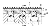
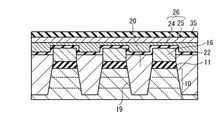
図26A及び図26Bは、本発明の不揮発性メモリの第8の実施の形態の構成を示す断面図である。ただし、図26Bは、図26AにおけるAA’断面図である。不揮発性メモリは、半導体基板10、ゲート絶縁層11、浮遊ゲート16、ポリシリコン層間絶縁層22、制御ゲート26、サイドウォール30、層間絶縁層35及び素子分離絶縁部20を具備する。ここでは、半導体基板10がP型の場合について説明するが、N型の場合も同様に適用可能である。
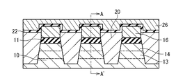
26A and 26B are cross-sectional views showing the configuration of the eighth embodiment of the nonvolatile memory of the present invention. However, FIG. 26B is an AA ′ sectional view in FIG. 26A. The nonvolatile memory includes a
図26Bを参照して、半導体基板10は、N型不純物をドープしたディープNウエル13と、半導体基板10表面側のP型不純物をドープしたPウエル14を備える。Pウエル14には、N型のソース27及びドレイン28が半導体基板10表面に接するように設けられている。ソース27とドレイン28との間の領域は、不揮発性メモリのチャネル領域8(第1領域)である。両者の距離は、例えば、150nmである。
Referring to FIG. 26B, the
第1絶縁層としてのゲート絶縁層11は、チャネル領域8とソース27及びドレイン28の各々の少なくとも一部とを覆うように設けられている。材質は、例えば、酸化シリコンである。膜厚は、電荷がトンネルすることが可能な大きさであり、例えば、10nmである。
The
電荷蓄積層としての浮遊ゲート16は、チャネル領域8上のゲート絶縁層11を覆うように設けられている。材質は、例えば、ポリシリコンである。膜厚は、例えば、250nmである。半導体基板10に平行な平面の大きさは、例えば150nm×150nmである。
The floating
第2絶縁層としてのポリシリコン層間絶縁層22は、浮遊ゲート16を覆うように設けられている。材質は、例えば、酸窒化シリコンや、酸化シリコン/窒化シリコン/酸化シリコンの積層膜である。膜厚は、例えば、30nmである。
The polysilicon
制御ゲート26は、ポリシリコン層間絶縁層22を覆うように設けられている。制御ゲート26は、シリサイド層25及びポリシリコン層24を備える。ポリシリコン層24は、ポリシリコン層間絶縁層22を覆うように設けられている。膜厚は、例えば、200nmである。シリサイド層25は、ポリシリコン層24を覆うように設けられている。材質は、例えば、CoSi2である。膜厚は、例えば、100nmである。
The
サイドウォール30は、浮遊ゲート16、ポリシリコン層間絶縁層22及び制御ゲート26の側面を覆い、下部がゲート絶縁層11に接するように設けられている。サイドウォール30は、引張応力を有する。そして、その引張応力により、チャネル領域8の圧縮応力を緩和することができる。特に、ゲート絶縁層11に接する部分及びそれと概ね平行な部分の引張応力の効果が大きい。サイドウォール30は、第1側壁絶縁層31、第2側壁絶縁層32及び第3側壁絶縁層33を備える。
The
第1側壁絶縁層31は、浮遊ゲート16、ポリシリコン層間絶縁層22及び制御ゲート26の側面を覆い、下部がゲート絶縁層11に接するように設けられている。材質は、例えば、酸化シリコンである。製造方法は、減圧CVD法に例示されるCVD法である。膜厚は、例えば、10nmである。
第2側壁絶縁層32は、第1側壁絶縁層31の表面を覆うように設けられている。例えば、窒化シリコン(SiN)、SiON膜、SiCN膜、AlO膜、及びAlSiN膜の少なくとも一つを含む膜である。製造方法は、減圧CVD法である。製膜温度は、600℃以上900℃以下が好ましい。この範囲では、膜に引張応力を持たせることができる。膜厚は、例えば、10nmである。
第3側壁絶縁層33は、第2側壁絶縁層32の表面を覆うように設けられている。材質は、例えば、酸化シリコンである。製造方法は、製造方法は、減圧CVD法に例示されるCVD法である。膜厚は、例えば、20nmである。これら第1側壁絶縁層31、第2側壁絶縁層32及び第3側壁絶縁層33の少なくとも一つが、特に、半導体基板10の表面に概ね平行な方向に引張応力を有することにより、チャネル領域8の圧縮応力を緩和することができる。
The first
The second
The third
第3絶縁層としての層間絶縁層35は、ゲート絶縁層11、サイドウォール30及び制御ゲート26を覆うように設けられている。例えば、窒化シリコン、SiON膜、SiCN膜、AlO膜、及びAlSiN膜の少なくとも一つを含む膜である。製造方法は、減圧CVD法のようなCVD法である。原料ガスは、シラン又はジクロルシランである。製膜温度は、膜質(膜に引張応力を持たせる条件)から600℃以上900℃以下が好ましい。膜厚は、例えば、200nmである。モノメチルシランとヒドラジンを原料ガスとして、CVD法で製膜しても良い。この層間絶縁層35は、引張応力を有する。そして、その引張応力により、チャネル領域8の圧縮応力を緩和することができる。
The interlayer insulating
図26Aを参照して、半導体基板10には、隣接する素子同士を分離する素子分離溝19が設けられ、素子分離絶縁部20が満たされている。素子分離絶縁部20は、STI(Shallow Trench Isolation)に例示される。その深さは、ディープNウエル13よりも深く設ける。材質は、例えば、酸化シリコンである。
Referring to FIG. 26A, the
図34〜図36については、第1の実施の形態と同様であるので、その説明を省略する。 34 to 36 are the same as those in the first embodiment, and thus the description thereof is omitted.
次に、本発明の不揮発性メモリの製造方法の第8の実施の形態について説明する。図2A及び図2B〜図8A及び図8B、図27A及び図27B〜図33A及び図33Bは、本発明の不揮発性メモリの製造方法の実施の形態の各ステップを説明する断面図である。ただし、各図における図Aと図Bとの関係は、図26A及び図26Bとの関係(各図Bは各図Aの図26におけるAA’断面)と同じである。 Next, an eighth embodiment of a method for manufacturing a nonvolatile memory according to the present invention will be described. 2A and 2B to FIG. 8A and FIG. 8B, and FIG. 27A and FIG. 27B to FIG. 33A and FIG. 33B are cross-sectional views illustrating each step of the embodiment of the method for manufacturing a nonvolatile memory according to the present invention. However, the relationship between FIG. A and FIG. B in each drawing is the same as the relationship between FIG. 26A and FIG. 26B (each drawing B is an AA ′ cross section in FIG. 26 of each drawing A).
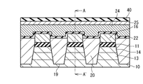
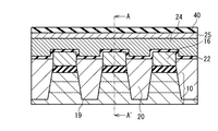
まず、不揮発性メモリの製造方法の第1の実施の形態に基づき、図2A及び図2B〜図8A及び図8Bに示される酸窒化シリコン膜22aの形成までを行う。
First, based on the first embodiment of the manufacturing method of the nonvolatile memory, the process up to the formation of the
次に、図27A及び図27Bを参照して、酸窒化シリコン膜22aを覆うように、CVD法で、ポリシリコン膜24aを300nmの膜厚で形成する。
Next, referring to FIGS. 27A and 27B, a
その後、図28A及び図28Bを参照して、フォトリソグラフィ及びエッチングの技術により、酸窒化シリコン膜22a及びポリシリコン膜24aをパターンニングして、ポリシリコン層24及びポリシリコン層間絶縁層22を形成する。
28A and 28B, the
図29A及び図29Bを参照して、ポリシリコン層24をマスクとして、N型不純物のイオン注入を行い、その後の熱処理により、ソース27及びドレイン28を形成する。
Referring to FIGS. 29A and 29B, N-type impurity ions are implanted using
図30A及び図30Bを参照して、ゲート絶縁層11及びポリシリコン層24を覆うように、CVD法で、サイドウォール用の酸化シリコン膜31a、窒化シリコン膜32a及び酸化シリコン膜33aをそれぞれ10nm、10nm及び20nmの膜厚で形成する。その時、引張応力を有するように、上述の製造条件を用いる。それにより、チャネル領域8の圧縮応力を低減することができる。
Referring to FIGS. 30A and 30B, the sidewall
図31A及び図31Bを参照して、異方性エッチングにより、サイドウォール30(第1側壁絶縁層31、第2側壁絶縁層32及び第3側壁絶縁層33)を形成する。
Referring to FIGS. 31A and 31B, sidewalls 30 (first
図32A及び図32Bを参照して、ポリシリコン層24を覆うように、スパッタ法で、Co膜を100nmの膜厚で製膜後、フォトリソグラフィ及びエッチングの技術により、ポリシリコン層24上にCo膜を残す。そして、熱処理によりポリシリコン層24と反応させ、100nm膜厚のCoSi2のシリサイド層25を形成する。これにより、制御ゲート26(シリサイド層25及びポリシリコン層24)を形成する。
Referring to FIGS. 32A and 32B, a Co film is formed to a thickness of 100 nm by sputtering so as to cover
図33A及び図33Bを参照して、ゲート絶縁膜11、サイドウォール30及び制御ゲート26を覆うように、CVD法で、層間絶縁膜35を200nmの膜厚で形成する。その時、引張応力を有するように、上述の製造条件を用いる。それにより、チャネル領域8の圧縮応力を低減することができる。
Referring to FIGS. 33A and 33B, an
上記製造方法により、図26A及び図26Bに示されるチャネル領域8の応力の小さい不揮発性メモリを製造することができる。
By the manufacturing method described above, a nonvolatile memory having a small stress in the
本実施の形態においても、第1の実施の形態で説明したものと同様の効果を得ることができる。 Also in this embodiment, the same effects as those described in the first embodiment can be obtained.
上記各実施の形態は、互いに矛盾が発生しない限り、重複して実施しても良い。 Each of the above embodiments may be repeated as long as no contradiction occurs.
8 チャネル領域
10 半導体基板
10a シリコン
10b シリコンゲルマニウム
11 ゲート絶縁膜
13 Nウエル
14 Pウエル
16 電荷蓄積層
16a 絶縁体
16b 半導体微粒子
17 窒化シリコン
18 強誘電体膜
20 素子分離絶縁部
20a 酸化シリコン
20b 窒化シリコン
20c 酸化シリコン
20d 酸化シリコン
22 層間絶縁膜
22a 酸窒化シリコン
24 ポリシリコン
24a ポリシリコン膜
25 金属
25a 金属膜
26 制御ゲート
27 ソース
28 ドレイン
29 炭素が添加されたシリコン
40 酸化シリコン
30 サイドウォール
31 第1側壁絶縁層
32 第2側壁絶縁層
33 第3側壁絶縁層
35 第2層間絶縁膜
8
Claims (36)
前記半導体基板内に前記ソース電極から離れて設けられたドレイン電極と、
前記ソース電極及び前記ドレイン電極の少なくとも一部、及び、前記ソース電極と前記ドレイン電極との間の第1領域を覆うように設けられた第1絶縁層と、
前記第1絶縁層を介して前記第1領域を覆うように設けられた電荷蓄積層と、
前記電荷蓄積層を覆うように設けられた第2絶縁層と、
前記第2絶縁層を覆うように設けられた制御ゲート電極と
を具備し、
前記第1領域における圧縮応力の大きさが、50MPa以下である
不揮発性メモリ。 A source electrode provided in a semiconductor substrate;
A drain electrode provided in the semiconductor substrate away from the source electrode;
A first insulating layer provided to cover at least a part of the source electrode and the drain electrode and a first region between the source electrode and the drain electrode;
A charge storage layer provided to cover the first region via the first insulating layer;
A second insulating layer provided to cover the charge storage layer;
A control gate electrode provided to cover the second insulating layer,
A non-volatile memory in which the magnitude of compressive stress in the first region is 50 MPa or less.
前記第1領域における引張応力の大きさが、50MPa以下である
不揮発性メモリ。 The non-volatile memory according to claim 1.
A non-volatile memory in which the magnitude of the tensile stress in the first region is 50 MPa or less.
前記制御ゲート電極は、前記第2絶縁層側から順に半導体膜、金属膜の積層構造を有する
不揮発性メモリ。 The nonvolatile memory according to claim 1 or 2,
The control gate electrode has a stacked structure of a semiconductor film and a metal film in order from the second insulating layer side.
前記金属膜は、タングステン、タンタル、モリブデン、窒化タングステン、窒化タンタル、及び窒化モリブデンのうちの少なくとも一つを含む
不揮発性メモリ。 The non-volatile memory according to claim 3,
The non-volatile memory, wherein the metal film includes at least one of tungsten, tantalum, molybdenum, tungsten nitride, tantalum nitride, and molybdenum nitride.
前記半導体基板の少なくとも一部が表面側から順にシリコン、シリコンゲルマニウムの積層構造を有する
不揮発性メモリ。 The nonvolatile memory according to any one of claims 1 to 4,
A nonvolatile memory in which at least a part of the semiconductor substrate has a stacked structure of silicon and silicon germanium in order from the surface side.
前記ソース電極及び前記ドレイン電極の少なくとも一方が、炭素が添加されたシリコンゲルマニウム及び炭素が添加されたシリコンのうちの少なくとも一方を含む
不揮発性メモリ。 The nonvolatile memory according to any one of claims 1 to 4,
A nonvolatile memory in which at least one of the source electrode and the drain electrode includes at least one of silicon germanium to which carbon is added and silicon to which carbon is added.
前記電荷蓄積層が、半導体薄膜である
不揮発性メモリ。 The nonvolatile memory according to any one of claims 1 to 6,
A nonvolatile memory in which the charge storage layer is a semiconductor thin film.
前記電荷蓄積層が電荷捕獲中心を含有する絶縁層である
不揮発性メモリ。 The nonvolatile memory according to any one of claims 1 to 6,
A nonvolatile memory, wherein the charge storage layer is an insulating layer containing charge trapping centers.
前記電荷捕獲中心を含有する絶縁層は、窒化シリコン、酸化アルミニウム、酸窒化アルミニウム、酸化ハフニウム、酸窒化ハフニウム、酸化シリコンハフニウム、酸窒化シリコンハフニウム、酸化ジルコニウム、酸窒化ジルコニウム、酸化シリコンジルコニウム、及び、酸窒化シリコンジルコニウムのうちの少なくとも一つである
不揮発性メモリ。 The nonvolatile memory according to claim 8,
The insulating layer containing the charge trapping center is silicon nitride, aluminum oxide, aluminum oxynitride, hafnium oxide, hafnium oxynitride, silicon hafnium oxide, silicon oxynitride hafnium, zirconium oxide, zirconium oxynitride, silicon zirconium oxide, and A non-volatile memory that is at least one of silicon zirconium oxynitride.
前記電荷蓄積層は、絶縁体薄膜と半導体微粒子とから形成される
不揮発性メモリ。 The nonvolatile memory according to any one of claims 1 to 6,
The charge storage layer is a non-volatile memory formed of an insulating thin film and semiconductor fine particles.
前記第2絶縁層を持たず、かつ、前記電荷蓄積層が強誘電体ある
不揮発性メモリ。 The nonvolatile memory according to any one of claims 1 to 6,
A non-volatile memory that does not have the second insulating layer and the charge storage layer is a ferroelectric.
前記第2絶縁層を持たず、かつ、前記電荷蓄積層が第1絶縁層側から順に金属、強誘電体の積層構造を有する
不揮発性メモリ。 The nonvolatile memory according to any one of claims 1 to 6,
A non-volatile memory that does not have the second insulating layer, and that the charge storage layer has a stacked structure of metal and ferroelectric in order from the first insulating layer side.
前記第1絶縁層と前記制御ゲート電極とを覆うように設けられた第3絶縁層と
を更に具備する
不揮発性メモリ。 The nonvolatile memory according to any one of claims 7 to 12,
A non-volatile memory further comprising: a third insulating layer provided to cover the first insulating layer and the control gate electrode.
前記第3絶縁膜は、引張応力を有する
不揮発性メモリ。 The non-volatile memory according to claim 13.
The third insulating film has a tensile stress.
前記第3絶縁膜は、SiN膜、SiON膜、SiCN膜、AlO膜、及びAlSiN膜の少なくとも一つを含む
不揮発性メモリ。 The nonvolatile memory according to claim 13 or 14,
The third insulating film includes a non-volatile memory including at least one of a SiN film, a SiON film, a SiCN film, an AlO film, and an AlSiN film.
前記電荷蓄積層、前記第2絶縁層及び前記制御ゲート電極の側面を覆い、下部が前記第1絶縁層に接するように設けられたサイドウォールを更に具備し、
前記サイドウォールは、
前記第1絶縁層に概ね平行な第1層と、
前記側面に概ね平行な第2層と
を備え、
前記第1層は、引張応力を有する
不揮発性メモリ。 The nonvolatile memory according to any one of claims 13 to 15,
A side wall that covers side surfaces of the charge storage layer, the second insulating layer, and the control gate electrode, and that has a lower portion in contact with the first insulating layer;
The sidewall is
A first layer generally parallel to the first insulating layer;
A second layer generally parallel to the side surface,
The first layer has a tensile stress.
前記第1層は、SiN膜、SiON膜、SiCN膜、AlO膜、及びAlSiN膜の少なくとも一つを含む
不揮発性メモリ。 The non-volatile memory according to claim 16,
The first layer includes a non-volatile memory including at least one of a SiN film, a SiON film, a SiCN film, an AlO film, and an AlSiN film.
前記半導体基板内に設けられた素子分離絶縁部を更に具備する
不揮発性メモリ。 The nonvolatile memory according to any one of claims 1 to 17,
A non-volatile memory further comprising an element isolation insulating part provided in the semiconductor substrate.
前記素子分離絶縁部は、少なくとも一部にシリコン窒化膜を含むトレンチ溝である
不揮発性メモリ。 The non-volatile memory according to claim 18,
The element isolation insulating portion is a trench groove including a silicon nitride film at least in part.
前記半導体基板の第1領域上の前記第1絶縁層を覆うように、電荷蓄積膜、第2絶縁層及び制御ゲート電極がこの順で積層された上部構造を形成するステップと、
前記半導体基板内において、ソース電極及びドレイン電極を、各々が前記第1領域に接し、互いに離れるように形成するステップと
を具備し、
前記上部構造を形成するステップは、
不揮発性メモリ製造後の前記第1領域における圧縮応力の大きさが50MPa以下、あるいは引張応力の大きさが50MPa以下であるように、前記制御ゲート電極として前記第2絶縁層側から順に半導体膜、金属膜の積層構造を形成するステップを備える
不揮発性メモリの製造方法。 Forming a first insulating layer on a semiconductor substrate;
Forming an upper structure in which a charge storage film, a second insulating layer, and a control gate electrode are stacked in this order so as to cover the first insulating layer on the first region of the semiconductor substrate;
Forming a source electrode and a drain electrode in the semiconductor substrate, each in contact with the first region and away from each other, and
Forming the superstructure comprises:
A semiconductor film as the control gate electrode in order from the second insulating layer side so that the magnitude of compressive stress in the first region after manufacturing the nonvolatile memory is 50 MPa or less, or the magnitude of tensile stress is 50 MPa or less, A method for manufacturing a nonvolatile memory, comprising: forming a stacked structure of metal films.
前記金属膜は、タングステン、タンタル、モリブデン、窒化タングステン、窒化タンタル、及び窒化モリブデンのうちの少なくとも一つを含む膜である
不揮発性メモリの製造方法。 The method of manufacturing a nonvolatile memory according to claim 20,
The method of manufacturing a nonvolatile memory, wherein the metal film is a film including at least one of tungsten, tantalum, molybdenum, tungsten nitride, tantalum nitride, and molybdenum nitride.
前記積層構造上に、第1絶縁層を形成するステップと、
前記半導体基板の第1領域上の前記第1絶縁層を覆うように、電荷蓄積膜、第2絶縁層及び制御ゲート電極がこの順で積層された上部構造を形成するステップと、
前記半導体基板内において、ソース電極及びドレイン電極を、各々が前記第1領域に接し、互いに離れるように形成するステップと
を具備し、
前記積層構造は、不揮発性メモリ製造後の前記第1領域における圧縮応力の大きさが50MPa以下、あるいは引張応力の大きさが50MPa以下となるように形成される
不揮発性メモリの製造方法。 Forming a stacked structure in which a silicon germanium film and a silicon film are stacked in this order on a semiconductor substrate;
Forming a first insulating layer on the laminated structure;
Forming an upper structure in which a charge storage film, a second insulating layer, and a control gate electrode are stacked in this order so as to cover the first insulating layer on the first region of the semiconductor substrate;
Forming a source electrode and a drain electrode in the semiconductor substrate, each in contact with the first region and away from each other, and
The method for manufacturing a nonvolatile memory, wherein the stacked structure is formed such that the magnitude of compressive stress in the first region after manufacturing the nonvolatile memory is 50 MPa or less, or the magnitude of tensile stress is 50 MPa or less.
前記シリコン基板の第1領域上の前記第1絶縁層を覆うように、電荷蓄積膜、第2絶縁層及び制御ゲート電極がこの順で積層された上部構造を形成するステップと、
前記シリコン基板内のソース電極及びドレイン電極となる部分の少なくとも一部に、炭素を添加したシリコンゲルマニウム膜及び炭素を添加したシリコン膜の少なくとも一方を形成するステップと、
前記シリコン基板内において前記ソース電極及び前記ドレイン電極を、各々が前記第1領域に接し、互いに離れるように形成するステップと
を具備し、
前記炭素を添加されたシリコンゲルマニウム膜及び前記炭素を添加されたシリコン膜は、不揮発性メモリ製造後の前記第1領域における圧縮応力の大きさが50MPa以下、あるいは引張応力の大きさが50MPa以下であるように形成される
不揮発性メモリの製造方法。 Forming a first insulating layer on a silicon substrate;
Forming an upper structure in which a charge storage film, a second insulating layer, and a control gate electrode are stacked in this order so as to cover the first insulating layer on the first region of the silicon substrate;
Forming at least one of a silicon germanium film to which carbon is added and a silicon film to which carbon is added to at least a part of portions to be a source electrode and a drain electrode in the silicon substrate;
Forming the source electrode and the drain electrode in the silicon substrate so as to be in contact with the first region and away from each other,
The silicon germanium film to which carbon is added and the silicon film to which carbon is added have a compressive stress of 50 MPa or less in a first region after manufacturing a nonvolatile memory, or a tensile stress of 50 MPa or less. A method for manufacturing a non-volatile memory formed as described above.
前記素子分離絶縁部以外の前記半導体基板上に第1絶縁層を形成するステップと、
前記半導体基板の第1領域上の前記第1絶縁層を覆うように、電荷蓄積膜、第2絶縁層及び制御ゲート電極がこの順で積層された上部構造を形成するステップと、
前記半導体基板内において,ソース電極及びドレイン電極を、各々が前記第1領域に接し、互いに離れるように形成するステップと
を具備し、
前記素子分離絶縁部を形成するステップは、
不揮発性メモリ製造後の前記第1領域における圧縮応力の大きさが50MPa以下、あるいは引張応力の大きさが50MPa以下であるように、前記素子分離絶縁部の少なくとも一部を窒化シリコン膜が含まれるトレンチ溝で形成するステップを備える
不揮発性メモリの製造方法。 Forming an element isolation insulating portion on the semiconductor substrate;
Forming a first insulating layer on the semiconductor substrate other than the element isolation insulating portion;
Forming an upper structure in which a charge storage film, a second insulating layer, and a control gate electrode are stacked in this order so as to cover the first insulating layer on the first region of the semiconductor substrate;
Forming a source electrode and a drain electrode in the semiconductor substrate, each in contact with the first region and away from each other,
The step of forming the element isolation insulating portion includes:
A silicon nitride film is included in at least a part of the element isolation insulating portion so that the magnitude of the compressive stress in the first region after manufacturing the nonvolatile memory is 50 MPa or less, or the magnitude of the tensile stress is 50 MPa or less. A method for manufacturing a non-volatile memory, comprising: forming a trench groove.
前記半導体基板の第1領域上の前記第1絶縁層を覆うように、電荷蓄積膜、第2絶縁層及び制御ゲート電極がこの順で積層された上部構造を形成するステップと、
前記半導体基板内において、ソース電極及びドレイン電極を、各々が前記第1領域に接し、互いに離れるように形成するステップと、
前記第1絶縁層上及び前記上部構造上に、前記第1領域における圧縮応力の大きさが50MPa以下、あるいは引張応力の大きさが50MPa以下であるように第3絶縁層を形成するステップと
を具備する
不揮発性メモリの製造方法。 Forming a first insulating layer on a semiconductor substrate;
Forming an upper structure in which a charge storage film, a second insulating layer, and a control gate electrode are stacked in this order so as to cover the first insulating layer on the first region of the semiconductor substrate;
Forming a source electrode and a drain electrode in the semiconductor substrate so as to be in contact with the first region and away from each other;
Forming a third insulating layer on the first insulating layer and on the upper structure so that the magnitude of compressive stress in the first region is 50 MPa or less, or the magnitude of tensile stress is 50 MPa or less; A method for manufacturing a nonvolatile memory.
前記第3絶縁層を形成するステップは、
シラン又はジクロルシランを原料ガスとして、CVD法で600℃以上の温度にて製膜するステップを備える
不揮発性メモリの製造方法。 The method of manufacturing a nonvolatile memory according to claim 25,
Forming the third insulating layer comprises:
A method for manufacturing a nonvolatile memory, comprising a step of forming a film at a temperature of 600 ° C. or higher by a CVD method using silane or dichlorosilane as a source gas.
前記第3絶縁層を形成するステップは、
モノメチルシランとヒドラジンを原料ガスとして、CVD法で製膜するステップを備える
不揮発性メモリの製造方法。 The method of manufacturing a nonvolatile memory according to claim 25,
Forming the third insulating layer comprises:
A method for manufacturing a nonvolatile memory, comprising: forming a film by a CVD method using monomethylsilane and hydrazine as source gases.
前記第1絶縁層上及び前記上部構造上に、第4絶縁層を形成するステップと、
前記第4絶縁層のうち、前記上部構造の側面を除いた部分を除去して、前記側面にサイドウォールを形成するステップと
を更に具備し、
前記サイドウォールは、引張応力を有する
不揮発性メモリの製造方法。 The method for manufacturing a nonvolatile memory according to any one of claims 25 to 27,
Forming a fourth insulating layer on the first insulating layer and on the upper structure;
Removing the portion of the fourth insulating layer except for the side surface of the upper structure to further form a sidewall on the side surface;
The sidewall has a tensile stress. A method for manufacturing a nonvolatile memory.
前記第3絶縁層及び前記サイドウォールのうちの少なくとも一方は、SiN膜、SiON膜、SiCN膜、AlO膜、及びAlSiN膜の少なくとも一つを含む
不揮発性メモリの製造方法。 The nonvolatile memory of claim 28,
At least one of the third insulating layer and the sidewall includes at least one of a SiN film, a SiON film, a SiCN film, an AlO film, and an AlSiN film.
前記上部構造を形成するステップは、
前記電荷蓄積膜として、半導体薄膜を形成するステップを備える
不揮発性メモリの製造方法。 The method for manufacturing a nonvolatile memory according to any one of claims 20 to 29,
Forming the superstructure comprises:
A method for manufacturing a nonvolatile memory, comprising: forming a semiconductor thin film as the charge storage film.
前記上部構造を形成するステップは、
前記電荷蓄積膜として、電荷捕獲中心を含有する絶縁膜を形成するステップを備える
不揮発性メモリの製造方法。 The method for manufacturing a nonvolatile memory according to any one of claims 20 to 29,
Forming the superstructure comprises:
A method for manufacturing a nonvolatile memory, comprising: forming an insulating film containing a charge trapping center as the charge storage film.
前記電荷捕獲中心を含有する前記絶縁膜を形成するステップが、
窒化シリコン、酸化アルミニウム、酸窒化アルミニウム、酸化ハフニウム、酸窒化ハフニウム、酸化シリコンハフニウム、酸窒化シリコンハフニウム、酸化ジルコニウム、酸窒化ジルコニウム、酸化シリコンジルコニウム、酸窒化シリコンジルコニウムのうちの少なくとも一つの薄膜を形成するステップを備える
不揮発性メモリの製造方法。 The method for manufacturing a nonvolatile memory according to claim 31,
Forming the insulating film containing the charge trapping center,
Forms a thin film of at least one of silicon nitride, aluminum oxide, aluminum oxynitride, hafnium oxide, hafnium oxynitride, silicon hafnium oxide, silicon hafnium oxynitride, zirconium oxide, zirconium oxynitride, silicon zirconium oxide, and silicon zirconium oxynitride A method for manufacturing a nonvolatile memory.
前記上部構造を形成するステップは、
前記電荷蓄積膜として、絶縁体と半導体微粒子とからなる薄膜を形成するステップを備える
不揮発性メモリの製造方法。 The method for manufacturing a nonvolatile memory according to any one of claims 20 to 29,
Forming the superstructure comprises:
A method for manufacturing a nonvolatile memory, comprising: forming a thin film made of an insulator and semiconductor fine particles as the charge storage film.
前記上部構造を形成するステップは、
前記電荷蓄積膜として、強誘電体薄膜を形成するステップを備え、前記第2絶縁層を形成するステップを有しない
不揮発性メモリの製造方法。 30. The method for manufacturing a nonvolatile memory according to claim 20, wherein:
Forming the superstructure comprises:
A non-volatile memory manufacturing method, comprising: forming a ferroelectric thin film as the charge storage film; and not forming the second insulating layer.
前記上部構造を形成するステップは、
前記電荷蓄積膜として、前記第1絶縁層側から順に、金属、強誘電体の積層構造を持つ薄膜を形成するステップを備え、前記第2絶縁層を形成するステップを有しない
不揮発性メモリの製造方法。 The method for manufacturing a nonvolatile memory according to any one of claims 20 to 29,
Forming the superstructure comprises:
Non-volatile memory manufacturing comprising the step of forming a thin film having a laminated structure of metal and ferroelectric in order from the first insulating layer side as the charge storage film, and not including the step of forming the second insulating layer Method.
前記上部構造を用いて自己整合的に素子分離領域を形成するステップを更に具備する
不揮発性メモリの製造方法。 The method for manufacturing a nonvolatile memory according to any one of claims 20 to 35,
A method of manufacturing a nonvolatile memory, further comprising the step of forming an element isolation region in a self-aligning manner using the upper structure.
Priority Applications (3)
| Application Number | Priority Date | Filing Date | Title |
|---|---|---|---|
| JP2004194150A JP2005294791A (en) | 2004-03-09 | 2004-06-30 | Nonvolatile memory and method of manufacturing nonvolatile memory |
| US11/074,064 US7064382B2 (en) | 2004-03-09 | 2005-03-08 | Nonvolatile memory and nonvolatile memory manufacturing method |
| CNA200510052703XA CN1667830A (en) | 2004-03-09 | 2005-03-09 | Nonvolatile memory and nonvolatile memory manufacturing method |
Applications Claiming Priority (2)
| Application Number | Priority Date | Filing Date | Title |
|---|---|---|---|
| JP2004065882 | 2004-03-09 | ||
| JP2004194150A JP2005294791A (en) | 2004-03-09 | 2004-06-30 | Nonvolatile memory and method of manufacturing nonvolatile memory |
Publications (1)
| Publication Number | Publication Date |
|---|---|
| JP2005294791A true JP2005294791A (en) | 2005-10-20 |
Family
ID=34921738
Family Applications (1)
| Application Number | Title | Priority Date | Filing Date |
|---|---|---|---|
| JP2004194150A Pending JP2005294791A (en) | 2004-03-09 | 2004-06-30 | Nonvolatile memory and method of manufacturing nonvolatile memory |
Country Status (3)
| Country | Link |
|---|---|
| US (1) | US7064382B2 (en) |
| JP (1) | JP2005294791A (en) |
| CN (1) | CN1667830A (en) |
Cited By (5)
| Publication number | Priority date | Publication date | Assignee | Title |
|---|---|---|---|---|
| JP2005268756A (en) * | 2004-03-17 | 2005-09-29 | Samsung Electronics Co Ltd | SONOS type memory device |
| JP2008210859A (en) * | 2007-02-23 | 2008-09-11 | Oki Electric Ind Co Ltd | Memory cell of nonvolatile semiconductor storage device |
| JP2009521100A (en) * | 2005-12-13 | 2009-05-28 | アプライド マテリアルズ インコーポレイテッド | Memory cell with stressed layer |
| JP2009164192A (en) * | 2007-12-28 | 2009-07-23 | Spansion Llc | Semiconductor device and manufacturing method thereof |
| US8134189B2 (en) | 2007-10-09 | 2012-03-13 | Fujitsu Semiconductor Limited | Semiconductor device and method of manufacturing the same |
Families Citing this family (30)
| Publication number | Priority date | Publication date | Assignee | Title |
|---|---|---|---|---|
| US7122222B2 (en) * | 2003-01-23 | 2006-10-17 | Air Products And Chemicals, Inc. | Precursors for depositing silicon containing films and processes thereof |
| JP4102334B2 (en) * | 2004-06-16 | 2008-06-18 | 株式会社東芝 | Semiconductor device and manufacturing method thereof |
| KR100643468B1 (en) * | 2005-12-01 | 2006-11-10 | 동부일렉트로닉스 주식회사 | Non-volatile memory device formed with insulating film spacer and manufacturing method thereof |
| US7544584B2 (en) | 2006-02-16 | 2009-06-09 | Micron Technology, Inc. | Localized compressive strained semiconductor |
| US8294224B2 (en) * | 2006-04-06 | 2012-10-23 | Micron Technology, Inc. | Devices and methods to improve carrier mobility |
| US7998809B2 (en) * | 2006-05-15 | 2011-08-16 | Micron Technology, Inc. | Method for forming a floating gate using chemical mechanical planarization |
| US7485544B2 (en) * | 2006-08-02 | 2009-02-03 | Micron Technology, Inc. | Strained semiconductor, devices and systems and methods of formation |
| US7968960B2 (en) | 2006-08-18 | 2011-06-28 | Micron Technology, Inc. | Methods of forming strained semiconductor channels |
| JP2008078376A (en) * | 2006-09-21 | 2008-04-03 | Oki Electric Ind Co Ltd | Semiconductor memory device |
| US7651915B2 (en) * | 2006-10-12 | 2010-01-26 | Infineon Technologies Ag | Strained semiconductor device and method of making same |
| US7671403B2 (en) * | 2006-12-06 | 2010-03-02 | Spansion Llc | P-channel NAND in isolated N-well |
| US8154107B2 (en) * | 2007-02-07 | 2012-04-10 | Taiwan Semiconductor Manufacturing Co., Ltd. | Semiconductor device and a method of fabricating the device |
| US20090096009A1 (en) * | 2007-10-16 | 2009-04-16 | Promos Technologies Pte. Ltd. | Nonvolatile memories which combine a dielectric, charge-trapping layer with a floating gate |
| US8710576B2 (en) * | 2008-02-12 | 2014-04-29 | Halo Lsi Inc. | High density vertical structure nitride flash memory |
| JP5269484B2 (en) * | 2008-05-29 | 2013-08-21 | 株式会社東芝 | Semiconductor memory device |
| JP5356005B2 (en) * | 2008-12-10 | 2013-12-04 | 株式会社東芝 | Nonvolatile semiconductor memory device and manufacturing method thereof |
| WO2010151856A2 (en) * | 2009-06-26 | 2010-12-29 | Cornell University | Chemical vapor deposition process for aluminum silicon nitride |
| KR20120026313A (en) * | 2010-09-09 | 2012-03-19 | 삼성전자주식회사 | Non-volatile memory device and method of fabricating the same |
| US9202930B2 (en) * | 2011-05-19 | 2015-12-01 | Freescale Semiconductor, Inc. | Memory with discrete storage elements |
| CN104716099B (en) * | 2013-12-13 | 2018-12-14 | 旺宏电子股份有限公司 | Non-volatile memory and its manufacturing method |
| US10651080B2 (en) | 2016-04-26 | 2020-05-12 | Lam Research Corporation | Oxidizing treatment of aluminum nitride films in semiconductor device manufacturing |
| US10049869B2 (en) * | 2016-09-30 | 2018-08-14 | Lam Research Corporation | Composite dielectric interface layers for interconnect structures |
| KR102616489B1 (en) | 2016-10-11 | 2023-12-20 | 삼성전자주식회사 | Method for fabricating semiconductor device |
| US9859153B1 (en) * | 2016-11-14 | 2018-01-02 | Lam Research Corporation | Deposition of aluminum oxide etch stop layers |
| US10879250B2 (en) * | 2017-08-29 | 2020-12-29 | Taiwan Semiconductor Manufacturing Company Ltd. | Semiconductor structure for memory device and method for forming the same |
| JP7089967B2 (en) * | 2018-07-17 | 2022-06-23 | ルネサスエレクトロニクス株式会社 | Semiconductor devices and their manufacturing methods |
| WO2020179006A1 (en) * | 2019-03-06 | 2020-09-10 | キオクシア株式会社 | Nonvolatile semiconductor storage device and method for manufacturing same |
| TWI738202B (en) * | 2019-06-03 | 2021-09-01 | 旺宏電子股份有限公司 | 3d flash memory and array layout thereof |
| US12022654B2 (en) | 2020-11-17 | 2024-06-25 | Macronix International Co., Ltd. | Memory device and method of manufacturing the same |
| US12550385B2 (en) * | 2022-03-04 | 2026-02-10 | International Business Machines Corporation | Contact resistance of nanosheet transistor |
Citations (10)
| Publication number | Priority date | Publication date | Assignee | Title |
|---|---|---|---|---|
| JPH07111293A (en) * | 1993-10-14 | 1995-04-25 | Mitsubishi Electric Corp | Nonvolatile memory device and manufacturing method thereof |
| JPH11150194A (en) * | 1997-11-17 | 1999-06-02 | Hitachi Ltd | Memory element by field effect element |
| JP2002009179A (en) * | 2000-06-21 | 2002-01-11 | Sony Corp | Nonvolatile semiconductor memory device and method of manufacturing the same |
| JP2002110932A (en) * | 2000-09-28 | 2002-04-12 | Toshiba Corp | Semiconductor device and manufacturing method thereof |
| WO2002063690A1 (en) * | 2001-02-08 | 2002-08-15 | Hitachi, Ltd. | Semiconductor integrated circuit device and its manufacturing method |
| JP2002319638A (en) * | 2001-04-23 | 2002-10-31 | Toshiba Corp | Semiconductor storage device |
| JP2002368139A (en) * | 2001-06-05 | 2002-12-20 | Matsushita Electric Ind Co Ltd | Non-volatile memory device |
| JP2003158241A (en) * | 2001-11-26 | 2003-05-30 | Hitachi Ltd | Semiconductor device and manufacturing method |
| JP2003229496A (en) * | 2002-02-05 | 2003-08-15 | Denso Corp | Method for fabricating semiconductor device |
| JP2003347543A (en) * | 2002-05-29 | 2003-12-05 | Toshiba Corp | Semiconductor device and manufacturing method thereof |
Family Cites Families (4)
| Publication number | Priority date | Publication date | Assignee | Title |
|---|---|---|---|---|
| JPH0831962A (en) | 1994-07-14 | 1996-02-02 | Hitachi Ltd | Method of manufacturing nonvolatile semiconductor memory device |
| JP4173672B2 (en) * | 2002-03-19 | 2008-10-29 | 株式会社ルネサステクノロジ | Semiconductor device and manufacturing method thereof |
| US6977408B1 (en) * | 2003-06-30 | 2005-12-20 | Lattice Semiconductor Corp. | High-performance non-volatile memory device and fabrication process |
| JP4449374B2 (en) * | 2003-09-04 | 2010-04-14 | 株式会社日立製作所 | Semiconductor device |
-
2004
- 2004-06-30 JP JP2004194150A patent/JP2005294791A/en active Pending
-
2005
- 2005-03-08 US US11/074,064 patent/US7064382B2/en not_active Expired - Fee Related
- 2005-03-09 CN CNA200510052703XA patent/CN1667830A/en active Pending
Patent Citations (10)
| Publication number | Priority date | Publication date | Assignee | Title |
|---|---|---|---|---|
| JPH07111293A (en) * | 1993-10-14 | 1995-04-25 | Mitsubishi Electric Corp | Nonvolatile memory device and manufacturing method thereof |
| JPH11150194A (en) * | 1997-11-17 | 1999-06-02 | Hitachi Ltd | Memory element by field effect element |
| JP2002009179A (en) * | 2000-06-21 | 2002-01-11 | Sony Corp | Nonvolatile semiconductor memory device and method of manufacturing the same |
| JP2002110932A (en) * | 2000-09-28 | 2002-04-12 | Toshiba Corp | Semiconductor device and manufacturing method thereof |
| WO2002063690A1 (en) * | 2001-02-08 | 2002-08-15 | Hitachi, Ltd. | Semiconductor integrated circuit device and its manufacturing method |
| JP2002319638A (en) * | 2001-04-23 | 2002-10-31 | Toshiba Corp | Semiconductor storage device |
| JP2002368139A (en) * | 2001-06-05 | 2002-12-20 | Matsushita Electric Ind Co Ltd | Non-volatile memory device |
| JP2003158241A (en) * | 2001-11-26 | 2003-05-30 | Hitachi Ltd | Semiconductor device and manufacturing method |
| JP2003229496A (en) * | 2002-02-05 | 2003-08-15 | Denso Corp | Method for fabricating semiconductor device |
| JP2003347543A (en) * | 2002-05-29 | 2003-12-05 | Toshiba Corp | Semiconductor device and manufacturing method thereof |
Cited By (6)
| Publication number | Priority date | Publication date | Assignee | Title |
|---|---|---|---|---|
| JP2005268756A (en) * | 2004-03-17 | 2005-09-29 | Samsung Electronics Co Ltd | SONOS type memory device |
| JP2009521100A (en) * | 2005-12-13 | 2009-05-28 | アプライド マテリアルズ インコーポレイテッド | Memory cell with stressed layer |
| JP2008210859A (en) * | 2007-02-23 | 2008-09-11 | Oki Electric Ind Co Ltd | Memory cell of nonvolatile semiconductor storage device |
| US8134189B2 (en) | 2007-10-09 | 2012-03-13 | Fujitsu Semiconductor Limited | Semiconductor device and method of manufacturing the same |
| US8551849B2 (en) | 2007-10-09 | 2013-10-08 | Fujitsu Semiconductor Limited | Semiconductor device and method of manufacturing the same |
| JP2009164192A (en) * | 2007-12-28 | 2009-07-23 | Spansion Llc | Semiconductor device and manufacturing method thereof |
Also Published As
| Publication number | Publication date |
|---|---|
| CN1667830A (en) | 2005-09-14 |
| US20050199945A1 (en) | 2005-09-15 |
| US7064382B2 (en) | 2006-06-20 |
Similar Documents
| Publication | Publication Date | Title |
|---|---|---|
| US7064382B2 (en) | Nonvolatile memory and nonvolatile memory manufacturing method | |
| JP5230274B2 (en) | Nonvolatile semiconductor memory device | |
| EP1912254B1 (en) | Vertical-channel FinFET SONOS memory and manufacturing method thereof | |
| KR100318683B1 (en) | Method of forming oxide/nitride/oxide dielectric layer | |
| US8278696B2 (en) | Semiconductor device and method of manufacturing the same | |
| US8115249B2 (en) | Nonvolatile semiconductor memory device and method for manufacturing the same | |
| JP5416936B2 (en) | Semiconductor device and manufacturing method thereof | |
| JP5806439B2 (en) | Memory cell and manufacturing method thereof | |
| US20070120179A1 (en) | SONOS type non-volatile memory devices having a laminate blocking insulation layer and methods of manufacturing the same | |
| JP6334268B2 (en) | Semiconductor device and manufacturing method thereof | |
| US8253190B2 (en) | Semiconductor device and method for manufacturing the same | |
| US20060246666A1 (en) | Method of fabricating flash memory with u-shape floating gate | |
| WO2010087265A1 (en) | Nonvolatile semiconductor storage device and method for manufacturing same | |
| CN106024889B (en) | Semiconductor device and method for manufacturing the same | |
| US8598001B2 (en) | Method for manufacturing twin bit structure cell with hafnium oxide and nano-crystalline silicon layer | |
| KR100905276B1 (en) | Flash memory device including multylayer tunnel insulator and method of fabricating the same | |
| CN101038893A (en) | Method for fabricating non-volatile memory element comprising shunt silicon layer | |
| CN119342837B (en) | Ferroelectric 3D NAND flash memory device, operation method and manufacturing method thereof | |
| US20080149988A1 (en) | Semiconductor memory devices and methods for fabricating the same | |
| KR101083418B1 (en) | Charge trap flash type nonvolatile memory device | |
| US20130256779A1 (en) | Method of manufacturing semiconductor device and semiconductor device | |
| US20100240209A1 (en) | Semiconductor devices including hydrogen implantation layers and methods of forming the same | |
| KR101327500B1 (en) | Flash memory devices including multi-layer tunnel insulator and method of fabricating the same | |
| TW521402B (en) | Method for reducing random bit failures of flash memories |
Legal Events
| Date | Code | Title | Description |
|---|---|---|---|
| A621 | Written request for application examination |
Free format text: JAPANESE INTERMEDIATE CODE: A621 Effective date: 20070522 |
|
| A977 | Report on retrieval |
Free format text: JAPANESE INTERMEDIATE CODE: A971007 Effective date: 20110228 |
|
| A131 | Notification of reasons for refusal |
Free format text: JAPANESE INTERMEDIATE CODE: A131 Effective date: 20110525 |
|
| A02 | Decision of refusal |
Free format text: JAPANESE INTERMEDIATE CODE: A02 Effective date: 20110926 |