JP2005294746A - Printed-circuit board and its manufacturing method - Google Patents
Printed-circuit board and its manufacturing method Download PDFInfo
- Publication number
- JP2005294746A JP2005294746A JP2004111207A JP2004111207A JP2005294746A JP 2005294746 A JP2005294746 A JP 2005294746A JP 2004111207 A JP2004111207 A JP 2004111207A JP 2004111207 A JP2004111207 A JP 2004111207A JP 2005294746 A JP2005294746 A JP 2005294746A
- Authority
- JP
- Japan
- Prior art keywords
- metal foil
- pattern
- adhesive
- conductive
- patterns
- Prior art date
- Legal status (The legal status is an assumption and is not a legal conclusion. Google has not performed a legal analysis and makes no representation as to the accuracy of the status listed.)
- Granted
Links
- 238000004519 manufacturing process Methods 0.000 title claims description 22
- 229910052751 metal Inorganic materials 0.000 claims abstract description 124
- 239000002184 metal Substances 0.000 claims abstract description 124
- 239000011888 foil Substances 0.000 claims abstract description 120
- 239000000853 adhesive Substances 0.000 claims abstract description 76
- 230000001070 adhesive effect Effects 0.000 claims abstract description 76
- 239000000758 substrate Substances 0.000 claims abstract description 24
- 239000002923 metal particle Substances 0.000 claims description 15
- BQCADISMDOOEFD-UHFFFAOYSA-N Silver Chemical compound [Ag] BQCADISMDOOEFD-UHFFFAOYSA-N 0.000 claims description 9
- 238000005530 etching Methods 0.000 claims description 9
- 238000003825 pressing Methods 0.000 claims description 9
- 238000000034 method Methods 0.000 claims description 8
- 238000010438 heat treatment Methods 0.000 claims description 7
- 239000002245 particle Substances 0.000 claims description 7
- 238000005520 cutting process Methods 0.000 claims description 6
- 238000005488 sandblasting Methods 0.000 claims description 4
- 239000002313 adhesive film Substances 0.000 description 15
- 229910052709 silver Inorganic materials 0.000 description 5
- 239000004332 silver Substances 0.000 description 5
- 239000004020 conductor Substances 0.000 description 3
- 238000007650 screen-printing Methods 0.000 description 3
- RYGMFSIKBFXOCR-UHFFFAOYSA-N Copper Chemical compound [Cu] RYGMFSIKBFXOCR-UHFFFAOYSA-N 0.000 description 2
- 239000000428 dust Substances 0.000 description 2
- 238000013508 migration Methods 0.000 description 2
- 230000005012 migration Effects 0.000 description 2
- 239000002244 precipitate Substances 0.000 description 2
- 238000007639 printing Methods 0.000 description 2
- 229910000906 Bronze Inorganic materials 0.000 description 1
- JOYRKODLDBILNP-UHFFFAOYSA-N Ethyl urethane Chemical compound CCOC(N)=O JOYRKODLDBILNP-UHFFFAOYSA-N 0.000 description 1
- OAICVXFJPJFONN-UHFFFAOYSA-N Phosphorus Chemical compound [P] OAICVXFJPJFONN-UHFFFAOYSA-N 0.000 description 1
- 239000003082 abrasive agent Substances 0.000 description 1
- NIXOWILDQLNWCW-UHFFFAOYSA-N acrylic acid group Chemical group C(C=C)(=O)O NIXOWILDQLNWCW-UHFFFAOYSA-N 0.000 description 1
- 239000010974 bronze Substances 0.000 description 1
- 239000003795 chemical substances by application Substances 0.000 description 1
- 239000011248 coating agent Substances 0.000 description 1
- 238000000576 coating method Methods 0.000 description 1
- 238000007796 conventional method Methods 0.000 description 1
- 229910052802 copper Inorganic materials 0.000 description 1
- 239000010949 copper Substances 0.000 description 1
- 239000011889 copper foil Substances 0.000 description 1
- KUNSUQLRTQLHQQ-UHFFFAOYSA-N copper tin Chemical compound [Cu].[Sn] KUNSUQLRTQLHQQ-UHFFFAOYSA-N 0.000 description 1
- 239000003822 epoxy resin Substances 0.000 description 1
- 239000000463 material Substances 0.000 description 1
- 229920000647 polyepoxide Polymers 0.000 description 1
- 239000004576 sand Substances 0.000 description 1
Images
Landscapes
- Printing Elements For Providing Electric Connections Between Printed Circuits (AREA)
- Structure Of Printed Boards (AREA)
Abstract
Description
本発明は、各種電子機器に使用されるプリント配線基板およびこの製造方法に係わり、特に導電パターンと金属箔パターンとを確実に接続することができるプリント配線基板およびこの製造方法に関する。 The present invention relates to a printed wiring board used in various electronic devices and a manufacturing method thereof, and more particularly to a printed wiring board capable of reliably connecting a conductive pattern and a metal foil pattern and a manufacturing method thereof.
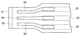
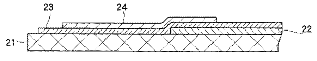
従来のプリント配線基板は、図10、図11に示すように、絶縁基板21上に複数の導電パターン22が形成され、これらの導電パターン22の端部側を被覆する面積が大きな異方性導電性接着膜23が配設されている。
また、異方性導電性接着膜23上で、複数の導電パターン22の端部と対向する部分には、複数の金属箔パターン24が、絶縁基板21の図示左端部方向に延出形成されている。即ち、導電パターン22と金属箔パターン24とは、異方性導電性接着膜23を介して電気的に接続している。
そして、、絶縁基板21の図示左端部方向に延びる金属箔パターン24の互いに隣り合う間隔寸法は、導電パターン22の互いに隣り合う間隔寸法より幅狭に形成されている。
As shown in FIGS. 10 and 11, the conventional printed wiring board has a plurality of
Further, on the anisotropic conductive
Further, the adjacent dimension of the
このような従来のプリント配線基板の製造方法は、図示を省略するが、まず最初に、所定の大きさからなる離型シートの全面にコートにより異方性導電性接着剤膜23を所定の厚さに形成する。即ち、異方性導電性接着剤膜23は、一方の面に剥離シートが張り付けされている。
その後、異方性導電性接着剤膜23の他方の面に、銅箔等からなる1枚の金属箔を貼り付ける。
In such a conventional method for manufacturing a printed wiring board, although not shown in the figure, first, an anisotropic conductive
Thereafter, one metal foil made of copper foil or the like is attached to the other surface of the anisotropic conductive
次ぎに、異方性導電性接着剤膜23の他方の面に貼り付けた1枚の金属箔を、エッチング加工により部分的に除去して、所定ピッチ寸法で複数の金属箔パターン24をパターン状に形成する。
続いて、金属箔パターン24が形成された異方性導電性接着剤膜23の他方の面側に、粘着力が弱い微粘着シートを貼り付ける。
即ち、異方性導電性接着剤膜23は、一方の面に離型シートが貼り付けられると共に、他方の面に複数の金属箔パターン24が形成されている。
Next, one metal foil attached to the other surface of the anisotropic conductive
Subsequently, a slightly adhesive sheet having a weak adhesive force is attached to the other surface side of the anisotropic conductive
That is, the anisotropic conductive
また、絶縁基板21の表面に、スクリーン印刷法により導電ペーストを印刷して導電パターン22を形成する。
次ぎに、剥離シートを剥離した異方性導電性接着剤膜23の一方の面を、絶縁基板21に重ね合わせる。
この時の導電パターン22と金属箔パターン24とは、異方性導電性接着剤膜23を介して互いに対向するように位置決めされている。
Further, the
Next, one surface of the anisotropic conductive
At this time, the
この状態で、所定温度に加熱した加圧ポンチを、金属箔パターン24を介して異方性導電性接着剤膜23を導電パター22および絶縁基板21の表面に圧接する。このことにより、金属箔パターン24が異方性導電性接着剤膜23を介して絶縁基板21表面に接着されると共に、導電パターン22と金属箔パターン24とが電気的に導通する。
また、互いに隣り合う金属箔パターン24間が異方性導電性接着剤膜23で絶縁されて、図10、図11に示すような従来のプリント配線基板が製造されている。
Further, the
しかし、従来のプリント配線基板は、異方性導電性接着剤膜23が高価であったので、コストアップになる問題があった。
本発明は、前述したような課題を解決するために、導電パターンと金属箔パターンとを低コストの絶縁性接着剤で接着して低価格のプリント配線基板を提供することを目的とする。
However, the conventional printed wiring board has a problem that the cost increases because the anisotropic conductive
In order to solve the problems described above, an object of the present invention is to provide a low-cost printed wiring board by bonding a conductive pattern and a metal foil pattern with a low-cost insulating adhesive.
前記課題を解決するための第1の解決手段として本発明のプリント配線基板は、絶縁基板上に形成した複数の導電パターンと、この複数の導電パターンにそれぞれ電気的に接続された複数の金属箔パターンとを備え、前記導電パターンと前記金属箔パターンとは、隣り合う前記導電パターン間、および隣り合う前記金属箔パターン間に位置する絶縁性の接着剤により接着されて、互いに電気的に接続されていることを特徴とする。 As a first means for solving the above problems, a printed wiring board according to the present invention includes a plurality of conductive patterns formed on an insulating substrate and a plurality of metal foils electrically connected to the plurality of conductive patterns, respectively. The conductive pattern and the metal foil pattern are bonded by an insulating adhesive located between the adjacent conductive patterns and between the adjacent metal foil patterns, and are electrically connected to each other. It is characterized by.
また、前記課題を解決するための第2の解決手段として、前記接着剤は、フィルム状に形成され、このフィルム状の接着剤を挟持した前記導電パターンおよび前記金属箔パターンの少なくとも前記金属箔パターンを加熱・加圧することにより、前記導電パターンと前記金属箔パターンとの間から押し出された前記接着剤が、前記隣り合う導電パターン間、および前記隣り合う金属箔パターン間に位置していることを特徴とする。 Further, as a second solving means for solving the problem, the adhesive is formed in a film shape, and at least the metal foil pattern of the conductive pattern and the metal foil pattern sandwiching the film-like adhesive. That the adhesive extruded from between the conductive pattern and the metal foil pattern is positioned between the adjacent conductive patterns and between the adjacent metal foil patterns. Features.
また、前記課題を解決するための第3の解決手段として、前記導体パターンには、金属粒子が含有され、前記金属粒子は、少なくとも銀粉が含有されていることを特徴とする。 Further, as a third solving means for solving the above-mentioned problem, the conductor pattern contains metal particles, and the metal particles contain at least silver powder.
また、前記課題を解決するための第4の解決手段として、前記導電パターンおよび前記金属箔パターンは、少なくとも互いに対向するいずれか一方の面が凹凸状に形成されていることを特徴とする。 Further, as a fourth solving means for solving the above-described problem, the conductive pattern and the metal foil pattern are characterized in that at least one of the surfaces facing each other is formed in an uneven shape.
また、前記課題を解決するための第5の解決手段として、前記導電パターンは、粒径の異なる少なくとも2種類の前記金属粒子を含有させた導電ペーストにより形成されていることを特徴とする。 As a fifth means for solving the problems, the conductive pattern is formed of a conductive paste containing at least two types of metal particles having different particle diameters.
また、前記課題を解決するための第6の解決手段として本発明のプリント配線基板の製造方法は、絶縁基板上に導電ペーストを印刷して複数の導電パターンを形成し、この導電パターン上に、フィルム状に形成された絶縁性の接着剤を介して複数の金属箔パターンを対向させて載置し、前記金属箔パターンを所定の温度と圧力で加熱・加圧して前記導電パターに圧接することにより、前記加熱で軟化した前記接着剤が前記導電パターンと前記金属パターンとの間から押し出されて、隣り合う前記導電パターン間、および隣り合う前記金属箔パターン間に位置し、前記導電性パターンと前記金属箔パターンとが前記接着剤で接着される共に、前記導電パターンと前記金属箔パターンとが電気的に接続されることを特徴とする。 Further, as a sixth means for solving the above problems, the printed wiring board manufacturing method of the present invention forms a plurality of conductive patterns by printing a conductive paste on an insulating substrate, and on the conductive patterns, A plurality of metal foil patterns are placed facing each other through an insulating adhesive formed in a film shape, and the metal foil patterns are heated and pressed at a predetermined temperature and pressure to be brought into pressure contact with the conductive pattern. The adhesive softened by heating is extruded from between the conductive pattern and the metal pattern, and is positioned between the adjacent conductive patterns and between the adjacent metal foil patterns, and the conductive pattern The metal foil pattern is bonded with the adhesive, and the conductive pattern and the metal foil pattern are electrically connected.
また、前記課題を解決するための第7の解決手段として、前記複数の金属箔パターンは、1枚の金属箔をプレス加工またはエッチング加工により短冊状に形成されて、前記接着剤の一方の面に所定のピッチ寸法で接着されていることを特徴とする。 Further, as a seventh solving means for solving the above problem, the plurality of metal foil patterns are formed in a strip shape by pressing or etching one metal foil, and one surface of the adhesive It is characterized in that it is bonded with a predetermined pitch dimension.
また、前記課題を解決するための第8の解決手段として、前記1枚の金属箔は、プレス加工またはエッチング加工により、両端部が連結部で連結された複数のスリット溝を形成し、このスリット溝が形成された前記1枚の金属箔を前記フィルム状の接着剤の一方の面に接着して前記連結部を切断することにより、前記接着剤の一方の面には、短冊状に分離された前記金属箔パターンが接着されて一体形成されることを特徴とする。 Further, as an eighth solving means for solving the above-mentioned problem, the one metal foil forms a plurality of slit grooves having both ends connected by a connecting portion by pressing or etching, and this slit By bonding the one metal foil with grooves formed on one surface of the film-like adhesive and cutting the connecting portion, the one surface of the adhesive is separated into strips. Further, the metal foil pattern is bonded and integrally formed.
また、前記課題を解決するための第9の解決手段として、前記接着剤は、前記一方の面と反対側の他方の面に剥離シートを貼着し、この剥離シートを剥離して、前記金属箔パターンを前記接着剤を介して前記導電パターンに加熱・加圧して圧接するようにしたことを特徴とする。 Further, as a ninth solving means for solving the above-mentioned problem, the adhesive has a release sheet attached to the other surface opposite to the one surface, the release sheet is peeled off, and the metal The foil pattern is heated and pressed against the conductive pattern via the adhesive and is press-contacted.
また、前記課題を解決するための第10の解決手段として、前記導電パターンと前記金属箔パターンとは、少なくともいずれか一方の互いに対向する面が、サンドブラスト加工により凹凸状に形成されていることを特徴とする。 Further, as a tenth solution means for solving the above-mentioned problem, at least one of the conductive pattern and the metal foil pattern is formed to be uneven by sandblasting. Features.
本発明のプリント配線基板は、導電パターンと金属箔パターンとは、隣り合う導電パターン間、および隣り合う金属箔パターン間に位置する絶縁性の接着剤により接着されて、互いに電気的に接続されているので、導電パターンと金属箔パターンとの端面を低コストの接着剤で強固に接着できる。そのために、低コストのプリンタ配線基板を提供できる。
また、導電パターンに、銀粉を含有させたとしても、隣り合うパターン間が絶縁性の接着剤で遮蔽されて、銀が析出するマイグレーションの発生を防止できる。
In the printed wiring board of the present invention, the conductive pattern and the metal foil pattern are bonded to each other by an insulating adhesive located between the adjacent conductive patterns and between the adjacent metal foil patterns, and are electrically connected to each other. Therefore, the end surfaces of the conductive pattern and the metal foil pattern can be firmly bonded with a low-cost adhesive. Therefore, a low-cost printer wiring board can be provided.
Moreover, even if silver powder is contained in the conductive pattern, the adjacent patterns are shielded by an insulating adhesive, and the occurrence of migration in which silver precipitates can be prevented.
また、接着剤は、フィルム状に形成され、このフィルム状の接着剤を挟持した導電パターンおよび金属箔パターンの少なくとも金属箔パターンを加熱・加圧することにより、導電パターンと金属箔パターンとの間から押し出された接着剤が、隣り合う導電パターン間、および隣り合う金属箔パターン間に位置しているので、導電パターンと金属箔パターンとの間から押し出された接着剤によって、導電パターンと金属箔パターンとを確実で強固に接着することができる。 In addition, the adhesive is formed in a film shape, and by heating / pressing at least the metal foil pattern of the conductive pattern and the metal foil pattern sandwiching the film-like adhesive, the adhesive is placed between the conductive pattern and the metal foil pattern. Since the extruded adhesive is located between the adjacent conductive patterns and between the adjacent metal foil patterns, the conductive pattern and the metal foil pattern are applied by the adhesive extruded from between the conductive pattern and the metal foil pattern. Can be securely and firmly bonded.
また、導体パターンには、金属粒子が含有され、前記金属粒子は、少なくとも銀粉が含有されているので、回路抵抗を低く抑えることができるプリント配線基板を提供できる。 Moreover, since the conductive pattern contains metal particles and the metal particles contain at least silver powder, it is possible to provide a printed wiring board that can keep circuit resistance low.
また、導電パターンおよび金属箔パターンは、少なくとも互いに対向するいずれか一方の面が凹凸状に形成されているので、金属箔パターンを導電パターンに加熱・加圧しても、表面の凹部に残った接着剤で、導電パターンと金属箔パターンとの端面だけでなく、互いに対向する平面部分でも接着することが、更に強固な接着力で導電パターンと金属箔パターンとを接着することができる。 In addition, since at least one of the conductive pattern and the metal foil pattern is formed in a concavo-convex shape, even if the metal foil pattern is heated and pressed to the conductive pattern, the adhesion remaining in the concave portion on the surface It is possible to bond the conductive pattern and the metal foil pattern with a stronger adhesive force by adhering not only the end surfaces of the conductive pattern and the metal foil pattern but also the planar portions facing each other.
また、導電パターンは、粒径の異なる少なくとも2種類の金属粒子を含有させた導電ペーストにより形成されているので、導電パターンの表面が凹凸状になって、凹部に適量の接着剤を残すことができる。そのために、導電パターンと金属箔パターンとの互いに対向する平面部分で強固に接着することができる。 In addition, since the conductive pattern is formed of a conductive paste containing at least two types of metal particles having different particle sizes, the surface of the conductive pattern may be uneven, leaving an appropriate amount of adhesive in the recess. it can. Therefore, it is possible to firmly bond the conductive pattern and the metal foil pattern at the mutually facing flat portions.
また、本発明のプリント配線基板の製造方法は、金属箔パターンを所定の温度と圧力で加熱・加圧して導電パターに圧着することにより、加熱で軟化した接着剤が導電パターンと金属パターンとの間から押し出されて、隣り合う導電パターン間、および隣り合う金属箔パターン間に位置し、導電性パターンと金属箔パターンとが接着剤で接着される共に、導電パターンと金属箔パターンとが電気的に接続されるので、製造が容易なプリント配線基板を提供できる。 Further, the printed wiring board manufacturing method of the present invention is a method in which the metal foil pattern is heated and pressed at a predetermined temperature and pressure and pressed onto a conductive pattern, so that the adhesive softened by heating is formed between the conductive pattern and the metal pattern. Extruded from above, located between adjacent conductive patterns and between adjacent metal foil patterns, the conductive pattern and the metal foil pattern are bonded with an adhesive, and the conductive pattern and the metal foil pattern are electrically connected Therefore, it is possible to provide a printed wiring board that can be easily manufactured.
また、複数の金属箔パターンは、1枚の金属箔をプレス加工またはエッチング加工により短冊状に形成されて、接着剤の一方の面に所定のピッチ寸法で接着されているので、金属箔パターンの取り扱いが容易となり、製造効率を向上させることができる。 In addition, the plurality of metal foil patterns are formed in a strip shape by pressing or etching one metal foil, and are bonded to one surface of the adhesive with a predetermined pitch dimension. Handling becomes easy and manufacturing efficiency can be improved.
また、1枚の金属箔は、プレス加工またはエッチング加工により、両端部が連結部で連結された複数のスリット溝を形成し、このスリット溝が形成された1枚の金属箔をフィルム状の接着剤の一方の面に接着して連結部を切断することにより、接着剤の一方の面には、短冊状に分離された金属箔パターンが接着されて一体形成されるので、金属パターンを容易に接着剤と一体形成することができる。 Further, one metal foil is formed by pressing or etching to form a plurality of slit grooves whose both ends are connected by a connecting portion, and the one metal foil having the slit grooves formed thereon is bonded to a film. By cutting the connecting part by bonding to one side of the agent, the metal foil pattern separated in a strip shape is bonded and integrally formed on one side of the adhesive, so the metal pattern can be easily formed It can be integrally formed with the adhesive.
また、接着剤は、一方の面と反対側の他方の面に剥離シートが貼着され、この剥離シートを剥離して、金属箔パターンを接着剤を介して導電パターンに加熱・加圧して圧接するようにしたので、導電パターン上に載置するまでのフィルム状の接着剤は、他方の面が剥離シートで覆われており、他方の面側にゴミ等が付着して接着力が低下するのを防止できる。 Also, the adhesive has a release sheet attached to the other side opposite to one side, the release sheet is peeled off, and the metal foil pattern is heated and pressed to the conductive pattern via the adhesive to press contact. Since the film adhesive until it is placed on the conductive pattern, the other surface is covered with a release sheet, and dust or the like adheres to the other surface, resulting in a decrease in adhesive strength. Can be prevented.
また、導電パターンと金属箔パターンとは、少なくともいずれか一方の互いに対向する面が、サンドブラスト加工により凹凸状に形成されているので、凹部に接着剤が残って導電パターンと金属箔パターンとを確実に接着することができる。 In addition, since at least one of the conductive pattern and the metal foil pattern is formed in an uneven shape by sandblasting, the adhesive remains in the concave portion to ensure the conductive pattern and the metal foil pattern. Can be glued to.
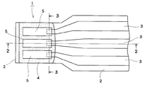
以下に、本発明のプリント配線基板およびこの製造方法について、図面に基づいて説明する。図1は本発明のプリント配線基板の平面図であり、図2は図1の2−2断面図であり、図3は図1の3−3断面図であり、図4は本発明に係わる接着剤に金属パターンを接着した平面図であり、図5は図4の5−5断面図であり、図6は、本発明に係わる金属箔パターンの製造方法を説明する金属箔の平面図であり、図7は本発明に係わる絶縁基板の平面図であり、図8は図7の8−8断面図であり、図9は本発明のプリント配線基板の製造方法を説明する概略図である。 Below, the printed wiring board of this invention and this manufacturing method are demonstrated based on drawing. 1 is a plan view of a printed wiring board according to the present invention, FIG. 2 is a cross-sectional view taken along the line 2-2 in FIG. 1, FIG. 3 is a cross-sectional view taken along the line 3-3 in FIG. FIG. 5 is a sectional view taken along line 5-5 in FIG. 4, and FIG. 6 is a plan view of the metal foil for explaining the method for producing the metal foil pattern according to the present invention. 7 is a plan view of an insulating substrate according to the present invention, FIG. 8 is a sectional view taken along the line 8-8 in FIG. 7, and FIG. 9 is a schematic view for explaining a method for manufacturing a printed wiring board according to the present invention. .
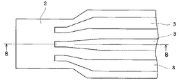
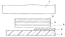
まず、本発明のプリント配線基板1は、図1〜図3に示すように、最下部にフレキシブル基板(FPC)からなる絶縁基板2が配設され、この絶縁基板2の上面に複数の導電パターン3が形成されている。
前記導電パターン3は、銀等の金属粒子を含有させた導電ペーストを、スクリーン印刷により図7に示すようなパターン状に所定厚さで形成されて、図示左端部側のピッチ寸法が図示右側のピッチ寸法よりも幅狭になっている。
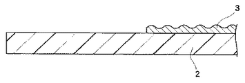
また、導電パターン2は、粒径の異なる少なくとも2種類の金属粒子を含有させた導電ペーストを用いて形成され、図8に示すように、表面が凹凸状になっている。
First, in the printed
The
Moreover, the
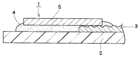
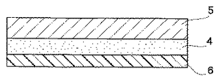
また、導電パターン3の図示左端部寄りの表面を含む絶縁基板2の図示左端部寄りの上面には、絶縁性の接着剤4が配設されている。この接着剤4は、例えば硬化時の収縮が小さなエポキシ樹脂材料、あるいはアクリル系、ウレタン系等を用いている。
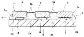
前記絶縁性の接着剤4は、図4、図5に示すように、所定厚さで面積の広いシート状に形成され、一方の面である上面には、形状が短冊状の複数の金属箔パターン5が、導電パターン3の左端部側のピッチ寸法と同じピッチ寸法で接着されている。
また、接着剤4の他方の面である下面側には、PET等のフィルムシートからなる剥離シート6が接着されて、接着剤4の下面側にゴミ等が付着しないようになっている。
An insulating
As shown in FIGS. 4 and 5, the insulating
Further, a
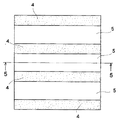
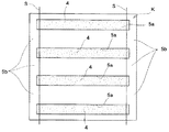
前記接一方の面に金属箔パターン5を張り付けした接着剤4の製造方法は、図6に示すような、銅またはリン青銅等の1枚の金属箔Kを、プレス加工、またはエッチング加工等により、所定の幅寸法と長さ寸法で複数のスリット溝5aを形成する。
前記スリット溝5aは、長手方向である図示左右両端部が、それぞれ連結部5bで連結されている。また、スリット溝5aは、ピッチ寸法が導電パターン3の左端部側のピッチ寸法と同じに形成されている。
このような複数のスリット溝5aが形成された金属箔Kは、下面側がシート状の接着剤4を介して剥離シート6に接着されて、スリット溝5aから接着剤4が露出している。
そして、金属箔Kは、図6に示すスリット溝5aの左右両端部寄りの切断線Sからプレス等で連結部5bを切断すると、図4、図5に示すように、短冊状に分離された複数の金属箔パターン5が接着剤4の一方の面に接着されて、接着剤4と金属箔パターン5、および剥離シート6が一体形成されている。
The manufacturing method of the adhesive 4 in which the
The
The metal foil K having such a plurality of
And when the
前記複数の金属箔パターン5を一方の面に接着したフィルム状の接着剤4は、剥離シート6を剥離して導電パターン3の図示左端部側を覆うように絶縁基板2上に載置して、金属箔パターン5を加熱・加圧することにより、導電パターン3と金属箔パターン5との間のフィルム状の接着剤4が軟化して、導電パターン3と金属箔パターン5との間から押し出される。
このことにより、導電パターン3と金属箔パターン5とが電気的に導通するようになっている。
The film-
As a result, the
また、導電パターン3と金属箔パターン5との間から押し出されて、隣り合う導電体パターン3間、および隣り合う金属箔パターン5間に位置する絶縁性の接着剤4によって、導電パターン3と金属箔パターン5とのそれぞれの端面3a、5aが所定の接着強度で接着されるようになっている。
また、導電パターン3は、粒径の異なる少なくとも2種類の金属粒子を含有させた導電ペーストで形成されて、表面が凹凸状になっているので、凹部に残った接着剤4によって、導電パターン3と金属箔パターン5との接着強度を更に強固にすることができる。
Further, the
In addition, the
尚、本発明の実施の形態では、金属箔Kを、図6に示すように、接着剤4と金属箔パターン5、および剥離シート6を一体化した状態で、左右両方の切断線Sから左右2箇所の連結部5bを切断することで説明したが、図示を省略するが、いずれか一方の切断線からいずれか一方の連結部5bを切断し、切断されてないいずれか他方の連結部5bの端部を絶縁基板2の図示左側の端部と位置合わせして張り合わせ、その後、切断されてない、いずれか他方の連結部5bを絶縁基板2の端部寄りも含めて切断するようにしても良い。
In the embodiment of the present invention, as shown in FIG. 6, the metal foil K is left and right from both the left and right cutting lines S in a state where the adhesive 4, the
このような構成の本発明のプリント配線基板1の製造方法は、銀等からなる粒径の異なる少なくとも2種類の金属粒子を含有させた導電ペーストを用いて、絶縁基板2の表面に複数の導電パターン3をスクリーン印刷等で形成する。
次ぎに、図9に示すように、短冊状の金属箔パターン5を一方の面に接着すると共に、他方の面に離型シート6を接着したフィルム状の接着剤4を、他方の面から剥離シート6を剥離して、導電パターン3の図示左端部上に載置する。
この時の接着剤4は、金属箔パターン5が接着剤4を介して導電パターン3と対向するように位置決めされている。
In the method for manufacturing the printed
Next, as shown in FIG. 9, the strip-shaped
The adhesive 4 at this time is positioned so that the
その後、温度を例えば略180°に上昇させた加圧ポンチ7により、金属箔パターン5を導電パターン3に所定の圧力で加圧することにより、接着剤4が温度上昇して軟化し、金属箔パターン5と導電パターン3との間から押し出される。
このことにより、金属箔パターン5と導電パターン3とが電気的に導通すると共に、金属箔パターン5と導電パターン3との間から押し出された接着剤4によって、金属箔パターン5と導電パターン3との幅方向の端面3a、5aが接着される。また、凹凸状に形成された導電パターン3の表面の凹部に残った接着剤4によって、更に強固に金属箔パターン5と導電パターン3とを接着することができる。
Thereafter, the
As a result, the
このような製造方法で製造された本発明のプリント配線基板1は、導電パターン3に低抵抗の銀からなる金属粒子を用いても、間隔が狭くなった図示左端部側の導電パターン3間に位置する絶縁性の接着剤4によって、銀が析出するマイグレーションの発生を防止できる。
また、本発明は、低コストの絶縁性の接着剤4を用いているので、低コストのプリント配線基板を提供できる。
In the printed
Moreover, since the low
尚、本発明の実施の形態では、粒径の異なる少なくとも2種類の金属粒子を含有させた導電ペーストを用いることによって、導電パターン3の表面を凹凸状にしたもので説明したが、導電パターン3と金属箔パターン5とは、少なくともいずれか一方の互いに対向する面が、砂あるいは砥粒材等を用いるサンドブラスト加工により凹凸状に形成したものでも良い。
また、金属箔パターン5の製造方法は、シート状の接着剤4に1枚の金属箔Kを接着し、その後、金属箔の一部をエッチング加工で短冊状の複数の金属箔5を形成したものでも良い。
In the embodiment of the present invention, the
Moreover, the manufacturing method of the
1 本発明のプリント配線基板
2 絶縁基板
3 導電パターン
4 接着剤
5 金属箔パターン
6 剥離シート
7 加圧ポンチ
DESCRIPTION OF
Claims (10)
The printed wiring according to any one of claims 6 to 9, wherein at least one of the conductive pattern and the metal foil pattern is formed in a concavo-convex shape by sandblasting. A method for manufacturing a substrate.
Priority Applications (1)
| Application Number | Priority Date | Filing Date | Title |
|---|---|---|---|
| JP2004111207A JP4427374B2 (en) | 2004-04-05 | 2004-04-05 | Printed wiring board and manufacturing method thereof |
Applications Claiming Priority (1)
| Application Number | Priority Date | Filing Date | Title |
|---|---|---|---|
| JP2004111207A JP4427374B2 (en) | 2004-04-05 | 2004-04-05 | Printed wiring board and manufacturing method thereof |
Publications (2)
| Publication Number | Publication Date |
|---|---|
| JP2005294746A true JP2005294746A (en) | 2005-10-20 |
| JP4427374B2 JP4427374B2 (en) | 2010-03-03 |
Family
ID=35327302
Family Applications (1)
| Application Number | Title | Priority Date | Filing Date |
|---|---|---|---|
| JP2004111207A Expired - Fee Related JP4427374B2 (en) | 2004-04-05 | 2004-04-05 | Printed wiring board and manufacturing method thereof |
Country Status (1)
| Country | Link |
|---|---|
| JP (1) | JP4427374B2 (en) |
Cited By (2)
| Publication number | Priority date | Publication date | Assignee | Title |
|---|---|---|---|---|
| WO2019035370A1 (en) * | 2017-08-14 | 2019-02-21 | 住友電工プリントサーキット株式会社 | Flexible printed wiring board |
| WO2019035278A1 (en) * | 2017-08-14 | 2019-02-21 | 住友電気工業株式会社 | Flexible printed wiring board |
Citations (8)
| Publication number | Priority date | Publication date | Assignee | Title |
|---|---|---|---|---|
| JPS62145602A (en) * | 1985-12-19 | 1987-06-29 | 住友ベークライト株式会社 | Conductive resin paste |
| JPH05152039A (en) * | 1991-09-27 | 1993-06-18 | Teikoku Tsushin Kogyo Co Ltd | Flexible board terminal structure |
| JPH11214450A (en) * | 1997-11-18 | 1999-08-06 | Matsushita Electric Ind Co Ltd | Electronic component package, electronic device using the same, and method of manufacturing electronic component package |
| JP2001119131A (en) * | 1999-10-20 | 2001-04-27 | Matsushita Electric Ind Co Ltd | Electronic component package, electronic device using the same, and method of manufacturing electronic component package |
| JP2003243788A (en) * | 2002-02-20 | 2003-08-29 | Alps Electric Co Ltd | Printed wiring board and manufacturing method of the same |
| JP2004039379A (en) * | 2002-07-02 | 2004-02-05 | Sumitomo Electric Ind Ltd | Conductive paste, conductive film, and method of manufacturing conductive film |
| JP2004039960A (en) * | 2002-07-05 | 2004-02-05 | Matsushita Electric Ind Co Ltd | Wiring board with terminals |
| JP2004079710A (en) * | 2002-08-14 | 2004-03-11 | Seiko Epson Corp | Semiconductor device and manufacturing method thereof, circuit board, and electronic apparatus |
-
2004
- 2004-04-05 JP JP2004111207A patent/JP4427374B2/en not_active Expired - Fee Related
Patent Citations (8)
| Publication number | Priority date | Publication date | Assignee | Title |
|---|---|---|---|---|
| JPS62145602A (en) * | 1985-12-19 | 1987-06-29 | 住友ベークライト株式会社 | Conductive resin paste |
| JPH05152039A (en) * | 1991-09-27 | 1993-06-18 | Teikoku Tsushin Kogyo Co Ltd | Flexible board terminal structure |
| JPH11214450A (en) * | 1997-11-18 | 1999-08-06 | Matsushita Electric Ind Co Ltd | Electronic component package, electronic device using the same, and method of manufacturing electronic component package |
| JP2001119131A (en) * | 1999-10-20 | 2001-04-27 | Matsushita Electric Ind Co Ltd | Electronic component package, electronic device using the same, and method of manufacturing electronic component package |
| JP2003243788A (en) * | 2002-02-20 | 2003-08-29 | Alps Electric Co Ltd | Printed wiring board and manufacturing method of the same |
| JP2004039379A (en) * | 2002-07-02 | 2004-02-05 | Sumitomo Electric Ind Ltd | Conductive paste, conductive film, and method of manufacturing conductive film |
| JP2004039960A (en) * | 2002-07-05 | 2004-02-05 | Matsushita Electric Ind Co Ltd | Wiring board with terminals |
| JP2004079710A (en) * | 2002-08-14 | 2004-03-11 | Seiko Epson Corp | Semiconductor device and manufacturing method thereof, circuit board, and electronic apparatus |
Cited By (6)
| Publication number | Priority date | Publication date | Assignee | Title |
|---|---|---|---|---|
| WO2019035370A1 (en) * | 2017-08-14 | 2019-02-21 | 住友電工プリントサーキット株式会社 | Flexible printed wiring board |
| WO2019035278A1 (en) * | 2017-08-14 | 2019-02-21 | 住友電気工業株式会社 | Flexible printed wiring board |
| JPWO2019035370A1 (en) * | 2017-08-14 | 2020-07-27 | 住友電工プリントサーキット株式会社 | Flexible printed wiring board |
| US11051399B2 (en) | 2017-08-14 | 2021-06-29 | Sumitomo Electric Industries, Ltd. | Flexible printed circuit board |
| JP7090622B2 (en) | 2017-08-14 | 2022-06-24 | 住友電工プリントサーキット株式会社 | Flexible printed wiring board |
| US11483928B2 (en) | 2017-08-14 | 2022-10-25 | Sumitomo Electric Printed Circuits, Inc. | Flexible printed circuit board |
Also Published As
| Publication number | Publication date |
|---|---|
| JP4427374B2 (en) | 2010-03-03 |
Similar Documents
| Publication | Publication Date | Title |
|---|---|---|
| JP7306594B1 (en) | Conductive film, wound body, connected structure, and method for manufacturing connected structure | |
| JP5152499B2 (en) | Electrical device and connection method thereof | |
| CN106304607B (en) | Rigid-flex board and manufacturing method thereof | |
| JP2010147442A (en) | Flexible printed wiring board, method of manufacturing the same, and flexible printed circuit board | |
| KR200442294Y1 (en) | Solderable Elastic Electrical Contact Terminals | |
| JP4427374B2 (en) | Printed wiring board and manufacturing method thereof | |
| CN204230234U (en) | Distribution component | |
| CN103517587B (en) | Rigid-flexible circuit board and preparation method thereof | |
| JP2005032815A (en) | Flexible wiring board and its manufacturing method | |
| JP5379710B2 (en) | Method for manufacturing flexible printed circuit board with reinforcing layer | |
| JP3305633B2 (en) | IC card manufacturing method | |
| JP3463539B2 (en) | Flexible circuit board with anisotropic conductive adhesive and manufacturing method | |
| KR20150114302A (en) | Connector and manufacturing method thereof | |
| JP2003243788A (en) | Printed wiring board and manufacturing method of the same | |
| JP5024190B2 (en) | IC module manufacturing method | |
| JP5581882B2 (en) | Flat cable and its manufacturing method | |
| JPH043117B2 (en) | ||
| JP4336617B2 (en) | Printed wiring board and manufacturing method thereof | |
| JP5217287B2 (en) | Flat cable manufacturing method | |
| JP2007273655A (en) | Flexible flat circuit board and manufacturing method thereof | |
| JP2505751Y2 (en) | Bending resistant thermocompression bonding member | |
| JPH0437523B2 (en) | ||
| WO2023189767A1 (en) | Individual piece processing adhesive film, method for manufacturing connecting structure, and connecting structure | |
| JP5040551B2 (en) | Non-contact type data carrier conductive member and method and apparatus for manufacturing the same | |
| JP2000067948A (en) | Adhesive anisotropic conductive film connector |
Legal Events
| Date | Code | Title | Description |
|---|---|---|---|
| A621 | Written request for application examination |
Free format text: JAPANESE INTERMEDIATE CODE: A621 Effective date: 20060901 |
|
| RD03 | Notification of appointment of power of attorney |
Free format text: JAPANESE INTERMEDIATE CODE: A7423 Effective date: 20080306 |
|
| A977 | Report on retrieval |
Free format text: JAPANESE INTERMEDIATE CODE: A971007 Effective date: 20090310 |
|
| A131 | Notification of reasons for refusal |
Free format text: JAPANESE INTERMEDIATE CODE: A131 Effective date: 20090331 |
|
| A521 | Written amendment |
Free format text: JAPANESE INTERMEDIATE CODE: A523 Effective date: 20090520 |
|
| A131 | Notification of reasons for refusal |
Free format text: JAPANESE INTERMEDIATE CODE: A131 Effective date: 20090623 |
|
| A521 | Written amendment |
Free format text: JAPANESE INTERMEDIATE CODE: A523 Effective date: 20090804 |
|
| TRDD | Decision of grant or rejection written | ||
| A01 | Written decision to grant a patent or to grant a registration (utility model) |
Free format text: JAPANESE INTERMEDIATE CODE: A01 Effective date: 20091124 |
|
| A01 | Written decision to grant a patent or to grant a registration (utility model) |
Free format text: JAPANESE INTERMEDIATE CODE: A01 |
|
| A61 | First payment of annual fees (during grant procedure) |
Free format text: JAPANESE INTERMEDIATE CODE: A61 Effective date: 20091214 |
|
| R150 | Certificate of patent or registration of utility model |
Free format text: JAPANESE INTERMEDIATE CODE: R150 |
|
| FPAY | Renewal fee payment (event date is renewal date of database) |
Free format text: PAYMENT UNTIL: 20121218 Year of fee payment: 3 |
|
| FPAY | Renewal fee payment (event date is renewal date of database) |
Free format text: PAYMENT UNTIL: 20131218 Year of fee payment: 4 |
|
| LAPS | Cancellation because of no payment of annual fees |