JP2005294740A - Multi-finger NMOS transistor structure - Google Patents
Multi-finger NMOS transistor structure Download PDFInfo
- Publication number
- JP2005294740A JP2005294740A JP2004111172A JP2004111172A JP2005294740A JP 2005294740 A JP2005294740 A JP 2005294740A JP 2004111172 A JP2004111172 A JP 2004111172A JP 2004111172 A JP2004111172 A JP 2004111172A JP 2005294740 A JP2005294740 A JP 2005294740A
- Authority
- JP
- Japan
- Prior art keywords
- nmos transistor
- finger
- resistance
- drain
- transistor structure
- Prior art date
- Legal status (The legal status is an assumption and is not a legal conclusion. Google has not performed a legal analysis and makes no representation as to the accuracy of the status listed.)
- Withdrawn
Links
Images

Landscapes
- Semiconductor Integrated Circuits (AREA)
Abstract
Description
本発明は、半導体集積回路における静電気破壊保護回路、特に、複数のゲート電極を有するマルチフィンガー型のNMOSトランジスタの構造に関する。 The present invention relates to an electrostatic breakdown protection circuit in a semiconductor integrated circuit, and more particularly to a structure of a multi-finger type NMOS transistor having a plurality of gate electrodes.
半導体集積回路の静電気保護素子としては、従来からPN接合ダイオードが用いられてきたが、近年の微細化の進展に伴い、MOSトランジスタのゲート酸化膜厚が、例えば、0.35μmのプロセスでは60〜70Å、0.25μmのプロセスでは40〜60Å、というように薄膜化してきている。 A PN junction diode has been conventionally used as an electrostatic protection element of a semiconductor integrated circuit. However, with the progress of miniaturization in recent years, the gate oxide film thickness of a MOS transistor is, for example, 60 to 60 mm in a process of 0.35 μm. In the process of 70 mm and 0.25 μm, the film thickness has been reduced to 40 to 60 mm.
このようにゲート酸化膜の薄膜化が進むと、低電圧化による動作が可能になる反面、静電気耐性が劣化してしまうという問題がある。従来のPNダイオードを用いた保護素子・回路では、PNダイオード自身のブレークダウン電圧がゲート酸化膜の耐圧より大きいこと、又、ブレークダウンする速さが静電気パルスに追従できないこと等から、ゲート酸化膜に損傷が生じてしまうため、近年ではマルチフィンガーNMOSトランジスタの寄生バイポーラトランジスタによるスナップバック特性を利用し、より積極的に静電気電荷を能動素子により消費する方法が用いられている(非特許文献1参照)。 As the gate oxide film becomes thinner in this way, the operation by lowering the voltage becomes possible, but there is a problem that the electrostatic resistance deteriorates. In a conventional protection element / circuit using a PN diode, the breakdown voltage of the PN diode itself is larger than the breakdown voltage of the gate oxide film, and the breakdown speed cannot follow the electrostatic pulse. In recent years, a method has been used in which electrostatic charges are more actively consumed by active elements using the snapback characteristics of parasitic bipolar transistors of multi-finger NMOS transistors (see Non-Patent Document 1). ).
図7(a)〜(c)、図8及び図9を用いて従来例を説明する。 A conventional example will be described with reference to FIGS. 7A to 7C, FIG. 8 and FIG.
図7(a)は通常用いられるマルチフィンガーNMOSトランジスタの平面図、図7(b)は断面図、図7(c)は寄生のNPNトランジスタまで含めた等価回路図である。図8はNMOSトランジスタのスナップバック特性を示す図、図9はフィンガー数が3の場合のマルチフィンガーNMOSトランジスタのスナップバック特性を示す図である。 7A is a plan view of a commonly used multi-finger NMOS transistor, FIG. 7B is a sectional view, and FIG. 7C is an equivalent circuit diagram including a parasitic NPN transistor. FIG. 8 is a diagram illustrating the snapback characteristics of the NMOS transistor, and FIG. 9 is a diagram illustrating the snapback characteristics of the multi-finger NMOS transistor when the number of fingers is three.
微細化されたMOSトランジスタでは、ソース・ドレイン抵抗が増加し性能が劣化するが、これを防ぐためにソース・ドレイン領域にシリサイドが形成され、ソース・ドレイン抵抗を低減させる手法が採られる。 In a miniaturized MOS transistor, the source / drain resistance increases and the performance deteriorates. In order to prevent this, silicide is formed in the source / drain region, and a method of reducing the source / drain resistance is adopted.
しかしながら、保護素子用のNMOSトランジスタにシリサイド構造を適用すると静電気耐性が劣化することが報告されており(非特許文献2参照)、静電気耐性劣化を防ぐために、通常シリサイド・ブロック技術により保護NMOSトランジスタのゲート電極(図7(a)の11)と静電気放電パルスが印加されるドレイン電極(図7(a)の13)との間にシリサイドを設けない領域(図7(a)の15)を設定する。マルチフィンガーNMOSトランジスタにシリサイド・ブロック技術を適用すると、シリサイド・
ブロックされた領域はバラスト抵抗として動作し、各フィンガーの動作均一性を促す。図7(c)及び図8は静電気放電パルスがドレイン領域に印加されたときのマルチフィンガーNMOSトランジスタの動作、所謂スナップバック特性を示す。
However, it has been reported that when a silicide structure is applied to an NMOS transistor for a protection element (see Non-Patent Document 2), in order to prevent the deterioration of the electrostatic resistance, the protection NMOS transistor is usually protected by a silicide block technology. A region (15 in FIG. 7A) where no silicide is provided is set between the gate electrode (11 in FIG. 7A) and the drain electrode to which the electrostatic discharge pulse is applied (13 in FIG. 7A). To do. When silicide block technology is applied to multi-finger NMOS transistors, silicide
The blocked area acts as a ballast resistor, facilitating the operational uniformity of each finger. FIGS. 7C and 8 show the so-called snapback characteristics of the multi-finger NMOS transistor when an electrostatic discharge pulse is applied to the drain region.
図9を用いてマルチフィンガーNMOSトランジスタの動作を説明する。
尚、図9はフィンガー数が3本の場合の例である。
The operation of the multi-finger NMOS transistor will be described with reference to FIG.
FIG. 9 shows an example in which the number of fingers is three.
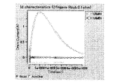
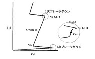
先ず、パッドに静電気放電パルスが印加されると、N型半導体であるドレイン部とP型半導体であるバックゲート部でアバランシェ・ブレークダウンが起こり、インパクト・イオン化により大量の電子−正孔対が発生し、電子はドレイン電界により引かれ、正孔はバックゲ−ト電位を上昇させるか、最低電位のソース電界に引かれる。バックゲート電位が、ソースをエミッタ、バックゲートをベース、ドレインをコレクタとする寄生NPNトランジスタのエミッタ−ベース間の順方向電圧より大きくなると、寄生NPNトランジスタが動作する。図9のVt1、It1はこの動作点である。寄生NPNトランジスタがONすると、ドレイン部の電流−電圧特性は寄生NMOSトランジスタのON抵抗に従ったものとなる。このとき注意すべき点は、以下の通りである。 First, when an electrostatic discharge pulse is applied to the pad, an avalanche breakdown occurs in the drain part which is an N-type semiconductor and the back gate part which is a P-type semiconductor, and a large number of electron-hole pairs are generated due to impact ionization. The electrons are attracted by the drain electric field, and the holes are attracted to the back gate potential or the lowest potential source electric field. When the back gate potential becomes higher than the forward voltage between the emitter and base of a parasitic NPN transistor having a source as an emitter, a back gate as a base, and a drain as a collector, the parasitic NPN transistor operates. Vt1 and It1 in FIG. 9 are these operating points. When the parasitic NPN transistor is turned on, the current-voltage characteristic of the drain portion follows the ON resistance of the parasitic NMOS transistor. The points to be noted at this time are as follows.
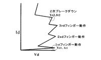
マルチフィンガーNMOSトランジスタでは、各ゲート毎に複数のNMOSトランジスタが並列に接続されてなるが、レイアウト的に全てのNMOSトランジスタに同じ構造を用いても、様々な不均一性(多くはプロセス的な)のために全てのNMOSトランジスタの寄生NPNトランジスタが同時にONすることはなく、必ず、或る1つのNMOSトランジスタの寄生NPNトランジスタがONすることから動作が始まる。このとき、各NMOSトランジスタのドレイン部は共通に接続されているので、各ドレイン電圧は一番最初に寄生NPNトランジスタがONしたNMOSトランジスタのドレイン電圧に追従した動作をすることになる(図9の1stフィンガー)。 In a multi-finger NMOS transistor, a plurality of NMOS transistors are connected in parallel for each gate. However, even if the same structure is used for all NMOS transistors in terms of layout, various non-uniformities (mostly process-like) Therefore, the parasitic NPN transistors of all the NMOS transistors are not turned on at the same time, and the operation always starts when the parasitic NPN transistor of one NMOS transistor is turned on. At this time, since the drain portions of the NMOS transistors are connected in common, each drain voltage operates so as to follow the drain voltage of the NMOS transistor in which the parasitic NPN transistor is turned on first (FIG. 9). 1st finger).
ドレイン電圧は動作している寄生NPNトランジスタのON抵抗に沿って上昇する。ON抵抗は、ソ−ス・ドレインの抵抗成分で、コンタクト抵抗、バラスト抵抗の値を含めたものとなる。ON抵抗での電圧上昇がVt1を超えると、2つ目のフィンガーで再びアバランシェ・ブレークダウンが起こり、バックゲート電位が上昇し、2つ目の寄生NPNトランジスタがONする。この結果、ON抵抗は2つの寄生NPNトランジスタのON抵抗の合成値となり、この抵抗に沿って3つ目の寄生NPNトランジスタがONするまで電位上昇が起こる。このようにして、全ての寄生NPNトランジスタを順次ONしていくことにより静電気放電パルスのエネルギーをON抵抗で消費される熱エネルギーに変換することで、MOSトランジスタのゲートを保護する。全ての寄生トランジスタがONすると、その合成ON抵抗に沿って電圧は上昇するが、熱暴走に至るまでに温度が上昇すると接合が損傷を受け(図9のVt2、It2)、接合でのリーク電流が増大する。 The drain voltage rises along the ON resistance of the operating parasitic NPN transistor. The ON resistance is a resistance component of the source / drain and includes the values of contact resistance and ballast resistance. When the voltage rise at the ON resistance exceeds Vt1, avalanche breakdown occurs again at the second finger, the back gate potential rises, and the second parasitic NPN transistor is turned on. As a result, the ON resistance becomes a composite value of the ON resistances of the two parasitic NPN transistors, and the potential rises along this resistance until the third parasitic NPN transistor is turned ON. In this way, the gate of the MOS transistor is protected by converting the energy of the electrostatic discharge pulse into the thermal energy consumed by the ON resistance by sequentially turning on all the parasitic NPN transistors. When all the parasitic transistors are turned on, the voltage increases along the combined ON resistance, but if the temperature rises until thermal runaway occurs, the junction is damaged (Vt2, It2 in FIG. 9), and the leakage current at the junction Will increase.
従って、熱暴走に至るまでに静電気放電エネルギーを全て消費することが必要である。 Therefore, it is necessary to consume all the electrostatic discharge energy before thermal runaway occurs.
しかしながら、このような構成によるとソース・ドレイン抵抗の最適化が困難であるという問題がある。即ち、寄生NPNトランジスタを順次ONさせるためには、ドレイン部のバラスト抵抗は大きい方が、ドレイン電圧がより早くVt1に到達するため望ましいが、大き過ぎるバラスト抵抗値はジュール熱による温度上昇による接合損傷を生じさせる。従って、バラスト抵抗での温度上昇の面からは抵抗値が低い方が良いが、抵抗値を下げることでドレイン電圧がVt1に達するのに時間が掛かり、その期間の電流集中による損傷の問題も発生する。特に、シリサイド部分は粒子状であり、電流が局所的に集中し易いため、容易に熱的損傷を受ける。 However, such a configuration has a problem that it is difficult to optimize the source / drain resistance. That is, in order to turn on the parasitic NPN transistors sequentially, it is preferable that the ballast resistance of the drain portion is large because the drain voltage reaches Vt1 earlier, but the ballast resistance value that is too large is damaged by the temperature rise due to Joule heat. Give rise to Therefore, the resistance value should be low from the viewpoint of temperature rise in the ballast resistor, but it takes time for the drain voltage to reach Vt1 by lowering the resistance value, and there is a problem of damage due to current concentration during that period. To do. In particular, the silicide portion is in the form of particles, and the current easily concentrates locally, so that it is easily damaged thermally.
これらのことから、ドレイン部の抵抗に最適な値が存在することは明らかであるが、ドレイン抵抗を構成するコンタクト抵抗、シリサイド部抵抗、シリサイド・ブロック領域(ドレイン・インプラント部)、更には、通常シリサイド・ブロック領域はマスクを用いるため、マスクずれの問題等、プロセスに非常に敏感であり、このため、静電気耐性にロットごとに差が生じるという問題もある。
本発明は、以上のような点に鑑みてなされたもので、プロセス変動に影響されにくく、且つ、マルチフィンガーNMOSトランジスタの寄生NPNトランジスタを、ほぼ同時にONさせるような静電気保護素子としてのマルチフィンガーNMOSトランジスタの構造を提供することを目的とする。
From these, it is clear that there is an optimum value for the resistance of the drain part, but the contact resistance, silicide part resistance, silicide block region (drain implant part) constituting the drain resistance, and usually Since the silicide block region uses a mask, it is very sensitive to the process, such as a mask displacement problem. For this reason, there is a problem that a difference in electrostatic resistance is generated for each lot.
The present invention has been made in view of the above points, and is a multi-finger NMOS as an electrostatic protection element that is not easily affected by process variations and that turns on the parasitic NPN transistor of the multi-finger NMOS transistor almost simultaneously. An object is to provide a transistor structure.
前述のような問題は、ドレイン部における電圧を、いわばドレイン抵抗が監視し、ドレイン電圧がVt1を超えた時点でアバランシェ・ブレークダウンを起すことを繰返していく過程で生じていることに着目すると、静電気放電パルスが印加された直後のアバランシェ・ブレークダウンに伴うインパクトイオン化によるバックゲート電位上昇を大きくし、寄生のNPNトランジスタがほぼ同時にトリガーされる状況が望ましく、このためにはバックゲート電位を、如何に上昇させるかが重要である。 Focusing on the fact that the above-mentioned problem occurs in the process of repeating the avalanche breakdown when the drain resistance is monitored by the drain resistance and the drain voltage exceeds Vt1. It is desirable to increase the back gate potential due to impact ionization associated with avalanche breakdown immediately after the electrostatic discharge pulse is applied, and the parasitic NPN transistor is triggered almost simultaneously. It is important to raise it.
インパクトイオン化に伴うバックゲート電位上昇を効率的にするためには、バックゲートのインピーダンスを大きくすることが有効であり、最もインピーダンスを高くするにはフローティング状態が望ましいが、完全なフローティング状態はラッチアップを誘発し易いため、望ましくない。 Increasing the back gate impedance is effective to efficiently increase the back gate potential due to impact ionization, and the floating state is desirable for the highest impedance, but the fully floating state is latched up. This is not desirable because it is easy to induce.
又、P基板においては、フローティング状態を造ることは不可能である。このため、インピーダンスを高めるためには、基板方向ではなく保護素子の側面を基板と切り離すような構造が必要となる。 Moreover, it is impossible to create a floating state in the P substrate. For this reason, in order to increase the impedance, a structure in which the side surface of the protection element is separated from the substrate instead of the substrate direction is required.
このために、CMOSプロセスにおいてPMOSトランジスタを製造する際に必須なN型のウェルによってNMOSトランジスタを取り囲むように構成し、
且つ、取り囲まれたP領域は底面のみで基板へ接続され、 金属配線では特定電位(殆どの場合最低電位)へ接続されないような構造とする。
For this purpose, the NMOS transistor is configured to be surrounded by an N-type well which is essential when manufacturing a PMOS transistor in a CMOS process.
In addition, the P region surrounded is connected to the substrate only at the bottom, and the metal wiring is not connected to a specific potential (in most cases, the lowest potential).
本発明によれば、マルチフィンガータイプの保護NMOSトランジスタをN型の拡散層で囲み、且つ、囲まれたバックゲート領域を金属配線で最低電位へ接続することなく基板との間に抵抗成分を持たせることで各フィンガー部の寄生NPNトランジスタのトリガー均一性を得ることができ、従来例のような1つの寄生NPNトランジスタへの電流集中を防ぎ、電流集中によるドレイン抵抗部の温度上昇を抑え、ジュール熱による接合破壊を防止することが可能になる。 According to the present invention, a multi-finger type protective NMOS transistor is surrounded by an N-type diffusion layer, and the enclosed back gate region has a resistance component between the substrate and the metal wiring without being connected to the lowest potential. By doing so, the trigger uniformity of the parasitic NPN transistor of each finger portion can be obtained, current concentration to one parasitic NPN transistor as in the conventional example is prevented, temperature rise of the drain resistance portion due to current concentration is suppressed, and Joule It becomes possible to prevent the junction breakage due to heat.
図1に本発明の実施の形態を示す。
図1はフィンガー数が4本の場合を示しているが、フィンガー数は多いほど2次ブレークダウン耐性が向上するので、通常は10本程度の場合が多い。
FIG. 1 shows an embodiment of the present invention.
Although FIG. 1 shows the case where the number of fingers is four, the higher the number of fingers, the more the secondary breakdown resistance is improved.
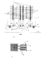
図1(a)本発明の実施の形態の断面図、図1(b)は平面図である。
図1(a),(b)において、11はフィンガーとなるゲート、12はソース、13はドレイン、14はソース、ドレイン部の抵抗を下げるためのサリサイド、15はバラスト抵抗に相当するサリサイドブロック、16は保護NMOSトランジスタを囲繞するN型の拡散層Nウェル、17はフィールド酸化膜、18は1のフィンガーを電気的に接続する金属配線、19はフィンガーごとに構成されるソース12を電気的に接続し、且つ、最低電位接続するための金属配線、110はフィンガーごとに構成されれる3のドレインを電気的に接続し、且つ、パッド111へ接続する金属配線、112は金属配線によってはどの電位へも接続されていない保護NMOSトランジスタのバックゲートである。
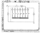
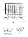
図2はシミュレーションで用いた回路図である。
FIG. 1A is a cross-sectional view of an embodiment of the present invention, and FIG. 1B is a plan view.
1A and 1B, 11 is a gate to be a finger, 12 is a source, 13 is a drain, 14 is a source, a salicide for reducing the resistance of the drain portion, 15 is a salicide block corresponding to a ballast resistor, 16 is an N-type diffusion layer N-well surrounding the protective NMOS transistor, 17 is a field oxide film, 18 is a metal wiring for electrically connecting one finger, and 19 is an
FIG. 2 is a circuit diagram used in the simulation.
図2において、NOはフィンガー数4のNMOSトランジスタを示しており、1はバックゲートで図1(a)のバックゲート112に相当する部分、2はゲートで図1(a)のゲート11へ、3,4,5はソースで図1(a)のソース12へ、6,7はドレインで図1(a)のドレイス13にそれぞれ相当する。R7はバックゲートと最低電位間のインピーダンス、R6はゲート抵抗、R1,R2,R4はソース直列抵抗、R3,R5はサリサイドブロック部のバラスト抵抗を含んだドレイン部の直列抵抗、VINは静電気放電パルスが印加される端子で、R0は人体帯電モデルの際の1.5kΩ抵抗を示す。
In FIG. 2, NO indicates an NMOS transistor having 4 fingers, 1 is a back gate, a portion corresponding to the
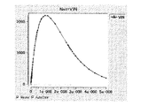
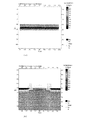
図3はシミュレーションで用いた人体帯電モデルの電圧波形図、図4(a),(b)はシミュレーションで用いたマルチフィンガーNMOSトランジスタの全体図及び1つのフィンガー部の拡大図である。 FIG. 3 is a voltage waveform diagram of the human body charging model used in the simulation, and FIGS. 4A and 4B are an overall view of the multi-finger NMOS transistor used in the simulation and an enlarged view of one finger portion.
このような構造において、先ずパッド111へ静電気放電パルスが印加されると、配線10、サリサイド4を経由してドレイン部3の電位は急激に上昇する。人体帯電モデルでは、およそ200v/nsec、2000vmaxの波形が1.5kΩの抵抗を通してパッド111へ印加される。
In such a structure, first, when an electrostatic discharge pulse is applied to the
急激に上昇したドレイン部の電圧は、バックゲートとの間でアバランシェ・ブレークダウンを起し、大量の電子−正孔対を生成し、生成された正孔がバックゲート電位を上昇させる。この電位がソース12をエミッタ、ドレイン13をコレクタ、バックゲート112をベースとする寄生NPNトランジスタのベース・エミッタ間順方向の閾値電圧を超えると寄生NPNトランジスタが動作し、図9に示すスナップバック特性を示すようになる。課題としているのは、フィンガー毎に存在する寄生のNPNトランジスタがほぼ同時にトリガーされ動作することであるが、図5及び図6にバックゲートへ接続される抵抗R7を0.1Ω、1kΩとした場合の各ドレイン電流波形を示している。
The drastically increased drain voltage causes avalanche breakdown with the back gate, generates a large number of electron-hole pairs, and the generated holes raise the back gate potential. When this potential exceeds the threshold voltage in the forward direction between the base and the emitter of the parasitic NPN transistor having the
図5はR7=0.1Ωの場合であるが、具体的にはバックゲートが金属配線により最低電位へ接続された状態を表している。 FIG. 5 shows a case where R7 = 0.1Ω, but specifically shows a state in which the back gate is connected to the lowest potential by a metal wiring.
ドレイン電流の一方は電流値がゼロであり、寄生NPNトランジスタが動作していないことが分かる。このことは、静電気放電パルスエネルギーを1つの寄生NPNトランジスタで消費しなくてはならず、この結果電流集中により、ドレイン抵抗に熱的損傷を引き起こすことを示している。
図6はR7=1kΩの場合であり、バックゲートはNウェルで囲まれ、基板方向のみで抵抗成分によって最低電位へ接続されている状態を示している。1〜2nsecの遅れ時間はあるが、2つのドレインにほぼ等しい電流が流れている、即ち、寄生NPNトランジスタがどちらも動作していることが分かり、この結果静電気放電パルスのエネルギーは両方の寄生NPNトランジスタでほぼ均等に消費されることを意味する。
One of the drain currents has a current value of zero, which indicates that the parasitic NPN transistor is not operating. This indicates that electrostatic discharge pulse energy must be consumed by one parasitic NPN transistor, resulting in thermal damage to the drain resistance due to current concentration.
FIG. 6 shows a case where R7 = 1 kΩ, and the back gate is surrounded by an N well and is connected to the lowest potential by a resistance component only in the substrate direction. Although there is a delay time of 1 to 2 nsec, it can be seen that approximately equal current flows through the two drains, i.e., both parasitic NPN transistors are operating, so that the energy of the electrostatic discharge pulse is reduced by both parasitic NPNs. It means that the transistors are consumed almost equally.
11 フィンガー(ゲート)
12 ドレイン
13 ソース
14 サリサイド
15 サリサイドブロック領域
16 N型拡散層
17 シリコン酸化膜
18 フィンガー配線
19 ソース配線
110 パッドからのドレイン配線
111 パッド
112 バックゲート
113 P型拡散層
11 Finger (Gate)
12
Claims (3)
前記半導体基板と反対導電型の拡散層をNMOSトランジスタを囲繞するように構成し、且つ、囲繞されたP型半導体領域を配線手段によっては、如何なる電位へも接続されないことを特徴とするマルチフィンガーNMOSトランジスタ構造。 An electrostatic breakdown protection element of a semiconductor integrated circuit configured on a P-type semiconductor substrate, and a multi-finger type NMOS having a plurality of gate electrodes,
A multi-finger NMOS characterized in that a diffusion layer having a conductivity type opposite to that of the semiconductor substrate is configured to surround an NMOS transistor, and the surrounded P-type semiconductor region is not connected to any potential by wiring means. Transistor structure.
Priority Applications (1)
| Application Number | Priority Date | Filing Date | Title |
|---|---|---|---|
| JP2004111172A JP2005294740A (en) | 2004-04-05 | 2004-04-05 | Multi-finger NMOS transistor structure |
Applications Claiming Priority (1)
| Application Number | Priority Date | Filing Date | Title |
|---|---|---|---|
| JP2004111172A JP2005294740A (en) | 2004-04-05 | 2004-04-05 | Multi-finger NMOS transistor structure |
Publications (1)
| Publication Number | Publication Date |
|---|---|
| JP2005294740A true JP2005294740A (en) | 2005-10-20 |
Family
ID=35327296
Family Applications (1)
| Application Number | Title | Priority Date | Filing Date |
|---|---|---|---|
| JP2004111172A Withdrawn JP2005294740A (en) | 2004-04-05 | 2004-04-05 | Multi-finger NMOS transistor structure |
Country Status (1)
| Country | Link |
|---|---|
| JP (1) | JP2005294740A (en) |
Cited By (3)
| Publication number | Priority date | Publication date | Assignee | Title |
|---|---|---|---|---|
| WO2014112294A1 (en) | 2013-01-18 | 2014-07-24 | セイコーインスツル株式会社 | Semiconductor device |
| TWI449157B (en) * | 2009-02-25 | 2014-08-11 | Univ Chien Hsin Sci & Tech | Design improvement of butting and inserted pickup in electrostatic discharge (esd) nmos's |
| JPWO2021140563A1 (en) * | 2020-01-07 | 2021-07-15 |
-
2004
- 2004-04-05 JP JP2004111172A patent/JP2005294740A/en not_active Withdrawn
Cited By (6)
| Publication number | Priority date | Publication date | Assignee | Title |
|---|---|---|---|---|
| TWI449157B (en) * | 2009-02-25 | 2014-08-11 | Univ Chien Hsin Sci & Tech | Design improvement of butting and inserted pickup in electrostatic discharge (esd) nmos's |
| WO2014112294A1 (en) | 2013-01-18 | 2014-07-24 | セイコーインスツル株式会社 | Semiconductor device |
| KR20150109359A (en) | 2013-01-18 | 2015-10-01 | 세이코 인스트루 가부시키가이샤 | Semiconductor device |
| JPWO2021140563A1 (en) * | 2020-01-07 | 2021-07-15 | ||
| WO2021140563A1 (en) * | 2020-01-07 | 2021-07-15 | 三菱電機株式会社 | High-frequency semiconductor device |
| JP7239023B2 (en) | 2020-01-07 | 2023-03-14 | 三菱電機株式会社 | high frequency semiconductor device |
Similar Documents
| Publication | Publication Date | Title |
|---|---|---|
| CN102456687B (en) | Semiconductor ESD device and method | |
| JP4290468B2 (en) | Electrostatic discharge protection element | |
| CN111009524B (en) | NMOS ESD protection device with gate boost | |
| US7986011B2 (en) | Electrostatic discharge protection device | |
| JP2007235151A (en) | Protection structure for integrated circuits | |
| JP2006319330A (en) | ESD protection device | |
| CN114783994A (en) | Integrated circuit element and protection method in electrostatic discharge event | |
| JP2005045016A (en) | Semiconductor integrated circuit | |
| CN100444378C (en) | Static protection circuit | |
| KR101043238B1 (en) | High Voltage Electrostatic Discharge Protection Devices | |
| US7145204B2 (en) | Guardwall structures for ESD protection | |
| US6949806B2 (en) | Electrostatic discharge protection structure for deep sub-micron gate oxide | |
| TWI278095B (en) | High voltage operating electrostatic discharge protection device | |
| JP2005294740A (en) | Multi-finger NMOS transistor structure | |
| CN103811482B (en) | Electrostatic discharge protection circuit | |
| JP2006313880A (en) | Electrostatic discharge circuit and integrated circuit having the same | |
| JP3123489B2 (en) | Electrostatic protection circuit in semiconductor integrated circuit and method of manufacturing the same | |
| JP2008172216A (en) | ESD protection by well potential trigger | |
| JP2007059543A (en) | ESD protection circuit and ESD protection circuit manufacturing method | |
| JP2005294691A (en) | Static electricity protection device in semiconductor integrated circuit | |
| KR100612948B1 (en) | Transistor of ESD Protection Circuit with Low Breakdown Voltage | |
| JP2009038189A (en) | Semiconductor device, voltage supply system, and semiconductor device manufacturing method | |
| JP2007242965A (en) | Semiconductor device | |
| JP4694123B2 (en) | Electrostatic discharge protection element | |
| KR20070058165A (en) | Electrostatic Discharge Protection Element of Semiconductor Device |
Legal Events
| Date | Code | Title | Description |
|---|---|---|---|
| RD01 | Notification of change of attorney |
Free format text: JAPANESE INTERMEDIATE CODE: A7421 Effective date: 20060201 |
|
| A300 | Withdrawal of application because of no request for examination |
Free format text: JAPANESE INTERMEDIATE CODE: A300 Effective date: 20070605 |