JP2005294679A - Solar cells - Google Patents
Solar cells Download PDFInfo
- Publication number
- JP2005294679A JP2005294679A JP2004109798A JP2004109798A JP2005294679A JP 2005294679 A JP2005294679 A JP 2005294679A JP 2004109798 A JP2004109798 A JP 2004109798A JP 2004109798 A JP2004109798 A JP 2004109798A JP 2005294679 A JP2005294679 A JP 2005294679A
- Authority
- JP
- Japan
- Prior art keywords
- interconnector
- back surface
- electrode
- solder
- collecting electrode
- Prior art date
- Legal status (The legal status is an assumption and is not a legal conclusion. Google has not performed a legal analysis and makes no representation as to the accuracy of the status listed.)
- Pending
Links
Images


Classifications
-
- Y—GENERAL TAGGING OF NEW TECHNOLOGICAL DEVELOPMENTS; GENERAL TAGGING OF CROSS-SECTIONAL TECHNOLOGIES SPANNING OVER SEVERAL SECTIONS OF THE IPC; TECHNICAL SUBJECTS COVERED BY FORMER USPC CROSS-REFERENCE ART COLLECTIONS [XRACs] AND DIGESTS
- Y02—TECHNOLOGIES OR APPLICATIONS FOR MITIGATION OR ADAPTATION AGAINST CLIMATE CHANGE
- Y02E—REDUCTION OF GREENHOUSE GAS [GHG] EMISSIONS, RELATED TO ENERGY GENERATION, TRANSMISSION OR DISTRIBUTION
- Y02E10/00—Energy generation through renewable energy sources
- Y02E10/50—Photovoltaic [PV] energy
Landscapes
- Photovoltaic Devices (AREA)
Abstract
【課題】従来の有鉛ハンダを使用している太陽電池では、有鉛ハンダを無鉛ハンダへ変更した場合、裏面集電電極とインターコネクタの接着後や、裏面集電電極とインターコネクタとのハンダ溶着部分からセルの割れやインターコネクタのハガレが発生し、太陽電池セルの性能および品質に悪影響を与えるという課題があった。
【解決手段】無鉛ハンダ処理をした際にハンダの付着量を確保する構成によりセルの割れやインターコネクタのハガレが発生しない太陽電池セルを提供するものである。
【選択図】図5
In a solar cell using a conventional leaded solder, when the leaded solder is changed to a lead-free solder, the solder between the back surface collecting electrode and the interconnector, or the solder between the back surface collecting electrode and the interconnector Cell cracks and interconnector peeling occurred from the welded portion, and there was a problem of adversely affecting the performance and quality of solar cells.
The present invention provides a solar battery cell that does not cause cracking of a cell or peeling of an interconnector due to a configuration that secures the amount of solder attached when lead-free soldering is performed.
[Selection] Figure 5
Description
本発明は、無鉛ハンダにて裏面電極を被覆された太陽電池セルとインターコネクタとのハンダ溶着方法に関するものである。 The present invention relates to a solder welding method between a solar battery cell whose back electrode is covered with lead-free solder and an interconnector.
従来のハンダ処理については、たとえば、特許文献1で開示している太陽電池及びその製造方法において、コレクター電極にハンダたまり部を形成することにより、ハンダの付着量を増加させるインターコネクタの接着強度手段等が知られていた。昨今ハンダは接合材料として使われているが、ハンダに含まれる鉛が生態系や人体に悪影響を及ぼすことが近年指摘されてきたため、電子部品や半導体部品などは、ハンダの無鉛化が進められており、太陽電池においても同様である。 As for conventional solder processing, for example, in the solar cell disclosed in Patent Document 1 and its manufacturing method, an interconnector adhesive strength means for increasing the amount of solder attached by forming a solder pool in the collector electrode Etc. were known. In recent years, solder has been used as a bonding material, but it has been pointed out in recent years that lead contained in solder has an adverse effect on the ecosystem and the human body. The same applies to solar cells.
そこで従来の太陽電池のハンダ処理について図6に基づいて説明をする。図6は従来型太陽電池セルにインターコネクタをハンダ溶着した状態を示す裏面側の平面図である。図6に示すように、従来型裏面集電電極102の線幅は、線幅が狭い部分を有した構成であったが、このハンダ被覆処理は有鉛ハンダでおこなっていたため、インターコネクタ14の取付による割れ・ハガレといった問題は発生しなかったが、無鉛ハンダを使用した場合には、従来型裏面集電電極102の形状の線幅が細い部分では、インターコネクタ14を接着した場合に端部の強度が弱くハガレが発生するケースもある。
従来の有鉛ハンダを使用している太陽電池では、太陽電池セルにおける集電電極とセル同士を連結するインターコネクタとを有鉛ハンダ溶着にて接着させている。そして、有鉛ハンダを無鉛ハンダへ変更した場合、裏面集電電極とインターコネクタの接着後や、裏面集電電極とインターコネクタとのハンダ溶着部分からセルの割れやインターコネクタのハガレが発生し、太陽電池セルの性能および品質に悪影響を与えるという課題があった。 In a solar battery using a conventional leaded solder, a current collecting electrode in a solar battery cell and an interconnector for connecting the cells are bonded together by leaded solder welding. And when leaded solder is changed to lead-free solder, after bonding of the back collector electrode and interconnector, cracking of the cell or peeling of the interconnector occurs from the solder welded part of the back collector electrode and interconnector, There existed a subject of having a bad influence on the performance and quality of a photovoltaic cell.
本発明は、従来の課題を解決するものであり、無鉛ハンダ処理のた際にハンダの付着量を確保する構成によりセルの割れやインターコネクタのハガレが発生しない太陽電池セルを提供することを目的としている。 An object of the present invention is to solve the conventional problems, and to provide a solar cell that does not cause cracking of a cell or peeling of an interconnector by a configuration that secures the amount of solder attached when lead-free soldering is performed. It is said.
請求項1記載の本発明は、結晶シリコン基板の受光面側に順次、拡散層、反射防止膜が積層され、同結晶シリコン基板の裏面側に、順次当該結晶シリコン基板と同伝導型の裏面電界層、裏面電極が積層され、かつ、前記受光面側に、光起電力を収集するためのバスバー電極とその各バスバー電極に対し直角に一定間隔で配列された複数本の細いグリッド電極で形成される表面集電電極と、前記裏面側に表面集電電極に対し、反対極性で形成される裏面集電電極とからなる太陽電池セルにおいて、裏面集電電極のハンダ被覆処理が無鉛ハンダにて構成され、前記裏面集電電極の線幅が、溶接するインターコネクタの幅よりも広く、かつ均一な線幅であることを特徴とする。 According to the first aspect of the present invention, a diffusion layer and an antireflection film are sequentially laminated on the light receiving surface side of the crystalline silicon substrate, and a back surface electric field of the same conductivity type as that of the crystalline silicon substrate is sequentially deposited on the back surface side of the crystalline silicon substrate. A layer and a back electrode are laminated, and on the light receiving surface side, a bus bar electrode for collecting photovoltaic power and a plurality of thin grid electrodes arranged at regular intervals at right angles to each bus bar electrode are formed. In the solar cell comprising the front surface current collecting electrode and the back surface current collecting electrode formed in the opposite polarity to the front surface current collecting electrode on the back surface side, the solder covering treatment of the back surface current collecting electrode is composed of lead-free solder The line collecting electrode has a line width wider than the interconnector to be welded and a uniform line width.
請求項2記載の本発明は、請求項1記載の太陽電池セルにおいて、裏面集電電極へ溶接するインターコネクタ端部の位置が、インターコネクタ長手方向の裏面集電電極端部から5.0mm以上の間隔を設けていることを特徴とする。 The present invention according to claim 2 is the solar cell according to claim 1, wherein the position of the end of the interconnector welded to the back collector electrode is 5.0 mm or more from the end of the back collector electrode in the longitudinal direction of the interconnector. An interval is provided.
請求項3記載の本発明は、請求項1記載の太陽電池セルにおいて、裏面集電電極の外部接続への出口部分近傍の線幅が広く形成されていることを特徴とする。 According to a third aspect of the present invention, in the solar cell according to the first aspect, the line width in the vicinity of the exit portion to the external connection of the back surface collecting electrode is formed wide.
請求項4記載の本発明は、請求項1記載の太陽電池セルにおいて、裏面集電電極へ溶接するインターコネクタ端部の位置が、インターコネクタ長手方向の裏面集電電極端部から5.0mm以上の間隔を設け、かつ前記裏面集電電極の外部接続への出口部分近傍の線幅が広く形成されていることを特徴とする。 According to a fourth aspect of the present invention, in the solar battery cell according to the first aspect, the position of the end of the interconnector welded to the back collector electrode is 5.0 mm or more from the end of the back collector electrode in the longitudinal direction of the interconnector. An interval is provided, and the line width in the vicinity of the exit portion to the external connection of the back surface collecting electrode is formed wide.
請求項5記載の本発明は、請求項1から請求項4いずれかに記載の太陽電池セルにおいて、裏面集電電極へ溶接するインターコネクタの厚み(銅厚)が100μm以下であることを特徴とする。 The present invention according to claim 5 is characterized in that, in the solar cell according to any one of claims 1 to 4, the thickness (copper thickness) of the interconnector welded to the back collector electrode is 100 μm or less. To do.
以上の説明から本発明によれば、裏面集電電極を無鉛ハンダにて被覆処理した太陽電池セルへのインターコネクタ溶着後や、インターコネクタを溶着させた太陽電池セルに発生する割れやハガレを防止することが可能となる。 From the above description, according to the present invention, after the interconnector is welded to the solar cell coated with the lead-free solder on the back surface collecting electrode, and the crack or peeling that occurs in the solar cell with the interconnector welded is prevented. It becomes possible to do.
本発明の第1の実施の形態は、太陽電池セルにおいて裏面集電電極のハンダ被覆処理が無鉛ハンダにて構成され、前記裏面集電電極の線幅が、溶接するインターコネクタの幅よりも広く、かつ均一な線幅である構成としたものである。この構成により、接着面積が拡大し、裏面集電電極とインターコネクタのハンダ接着部分のハンダ付着量を増加して、接着強度を向上させたものである。 In the first embodiment of the present invention, in the solar battery cell, the solder covering treatment of the back surface collecting electrode is constituted by lead-free solder, and the line width of the back surface collecting electrode is wider than the width of the interconnector to be welded. And a uniform line width. With this configuration, the adhesion area is increased, the amount of solder adhesion at the solder adhesion portion of the back collector electrode and the interconnector is increased, and the adhesion strength is improved.
本発明の第2の実施の形態は、第1の実施の形態における太陽電池セルにおいて、裏面集電電極へ溶接するインターコネクタ端部の位置が、インターコネクタ長手方向の裏面集電電極端部から5.0mm以上の間隔を設けて溶接する構成としたものである。これにより、インターコネクタの線端部でのハンダの強度不足等の問題を避けている。 In the second embodiment of the present invention, in the solar battery cell according to the first embodiment, the position of the end of the interconnector welded to the back collector electrode is 5 from the end of the back collector electrode in the longitudinal direction of the interconnector. The welding is performed with an interval of 0.0 mm or more. This avoids problems such as insufficient solder strength at the end of the interconnector.
本発明の第3の実施の形態は、第1の実施の形態における太陽電池セルにおいて、裏面集電電極の外部接続への出口部分近傍の線幅が広い構成としたものである。この構成により、最も強度のかかる裏面集電電極の出口部分近傍のハンダ付着量を増加して、接着強度を向上させたものである。 The third embodiment of the present invention has a configuration in which the line width in the vicinity of the outlet portion to the external connection of the back surface collecting electrode is wide in the solar battery cell in the first embodiment. With this configuration, the adhesion strength is improved by increasing the amount of solder attached in the vicinity of the outlet portion of the back surface collecting electrode, which is the strongest.
本発明の第4の実施の形態は、第1の実施形態である太陽電池セルにおいて、裏面集電電極へ溶接するインターコネクタ端部の位置が、インターコネクタ長手方向の裏面集電電極端部から5.0mm以上の間隔を設け、かつ前記裏面集電電極の外部接続への出口部分近傍の線幅が広い構成としたものである。これにより、インターコネクタの線端部でのハンダの強度不足等の問題を解決し、かつ裏面集電電極の出口部分近傍のハンダ付着量を増加して接着強度を向上させたものである。 According to the fourth embodiment of the present invention, in the solar battery cell according to the first embodiment, the position of the end of the interconnector welded to the back collector electrode is 5 from the end of the back collector electrode in the longitudinal direction of the interconnector. A space of 0.0 mm or more is provided, and the line width in the vicinity of the exit portion to the external connection of the back surface collecting electrode is wide. This solves problems such as insufficient solder strength at the line end of the interconnector and increases the adhesion amount by increasing the amount of solder attached in the vicinity of the outlet portion of the back collecting electrode.
本発明の第5の実施の形態は、第1から第4の実施の形態における太陽電池セルにおいて、表面集電電極と裏面集電電極へ溶接するインターコネクタの厚み(銅厚)が100μm以下の構成とし、温度負荷によるインターコネクタ内部の銅板の伸縮を緩和させるようにしたものである。 According to the fifth embodiment of the present invention, in the solar cells in the first to fourth embodiments, the thickness (copper thickness) of the interconnector welded to the front collector electrode and the rear collector electrode is 100 μm or less. In this configuration, expansion and contraction of the copper plate inside the interconnector due to temperature load is alleviated.
以下、本発明の実施例について図面を参照しながら説明する。 Embodiments of the present invention will be described below with reference to the drawings.
(実施例1)
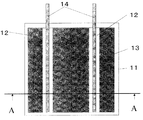
本発明の実施例1について、図1から図2に基づいて説明をおこなう。図1は本発明の実施例1にて太陽電池セルにインターコネクタをハンダ溶着した裏面側の状態を示す平面図、図2は図1の太陽電池セル11のA−A断面図である。
(Example 1)
A first embodiment of the present invention will be described with reference to FIGS. FIG. 1 is a plan view showing a state of a back surface side where an interconnector is soldered to a solar battery cell in Example 1 of the present invention, and FIG. 2 is a cross-sectional view taken along line AA of the
図1に示すように、太陽電池セル11の裏面には裏面電極13と裏面集電電極12が2本それぞれ印刷され、その裏面集電電極12の表面はハンダ被覆されている。そして、裏面集電電極12の線幅は、太陽電池セル同士を接続するインターコネクタ14の線幅の左右に一定の幅を設けた構成としている。
As shown in FIG. 1, two
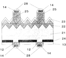
また、図2は図1の太陽電池セル11のA−A断面図である。結晶シリコン基板21の受光面側に順次、拡散層22、反射防止膜23が積層され、同結晶シリコン基板の裏面側に、順次当該結晶シリコン基板21と同伝導型の裏面電界層24、裏面電極13が積層され、かつ、前記受光面側に、光起電力を収集するため表面集電電極25と、前記裏面側に、表面集電電極25に対し反対極性で形成される裏面集電電極12とからなり、その裏面集電電極12の線幅は、前記インターコネクタ14の線幅の左右に一定の幅を設けている。そして、裏面集電電極12のハンダ被覆処理28上にハンダ溶着にてインターコネクタ14が取付けられた構成となっている。
FIG. 2 is a cross-sectional view taken along the line AA of the
このインターコネクタ14の取り付けは、太陽電池セル11を加熱し、そのハンダを溶かし、溶けたハンダの上に、インターコネクタ14を置いて加圧することで接着される際、インターコネクタ14の線幅の左右にもハンダを付着させている。
When the
そのため、セルの割れやインターコネクタのハガレの原因の一つと考えられる温度負荷によるインターコネクタの伸縮が発生しても、インターコネクタ14を接着した時に長手方向の両端面のハンダ付着量が増加しているため、接着強度が向上し、割れやハガレを抑制できる。
For this reason, even if the interconnector expands or contracts due to temperature load, which is considered to be one of the causes of cell cracking and interconnector peeling, the amount of solder attached to both end surfaces in the longitudinal direction increases when the
つまり、従来の有鉛ハンダと無鉛ハンダを比べると、有鉛ハンダのほうが柔らかい性質を持っているため、ハンダ接着面積が少なくても十分な接着力を確保できていた。しかし、ハンダが無鉛ハンダの場合には、有鉛ハンダに比べて、硬くもろい性質を持っているため、インターコネクタ14の伸縮による応力が吸収できず、結晶シリコン基板21へダメージを与えるためセル割れやハガレ発生に対してハンダ付着量を確保する構成としたものである。
In other words, when compared with conventional leaded solder and lead-free solder, leaded solder has a softer property, so that sufficient adhesive force can be secured even if the solder bonding area is small. However, when the solder is lead-free solder, it has a hard and brittle nature compared to leaded solder, so that stress due to expansion / contraction of the
(実施例2)
実施例2は、実施例1と裏面集電電極12にインターコネクタ14を取り付ける位置が相違し、実施例1で説明したものと同じ記号等は省略するものとする。
(Example 2)
In Example 2, the position where the
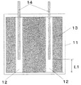
図3は本発明の実施例2にて太陽電池セルにインターコネクタ14をハンダ溶着した状態を示す裏面側の平面図である。図3に示すように、インターコネクタ14を裏面集電電極12に取り付ける位置を、裏面集電電極12の端部から5.0mm以上L1の間隔を設けて接着している。
FIG. 3 is a plan view on the back surface side showing a state in which the
これにより、裏面集電電極12の端部からのセルの割れやインターコネクタのハガレの原因の一つと考えられる温度負荷によるインターコネクタの伸縮が発生した場合でも、インターコネクタ14の端部と裏面集電電極12の端部が離れた位置にあるため、応力が分散され、かつハンダ付着量の増加により、接着強度も向上するため、割れやハガレを抑制することができる。
As a result, even when the interconnector expands or contracts due to a temperature load that is considered to be one of the causes of cracking of the cell from the end of the back
(実施例3)
実施例3は、実施例1と裏面集電電極12に対して出口部分が拡大した出口拡大部42の構成が相違したものであり、実施例1で説明したものと同じ記号等は省略する。
(Example 3)
The third embodiment is different from the first embodiment in the configuration of the outlet enlarged
図4は本発明の実施例3にて太陽電池セルにインターコネクタをハンダ溶着した状態を示す裏面側の平面図である。図4に示す裏面集電電極12の出口拡大部42は、インターコネクタ14を外部接続に取り出す出口側で、裏面集電電極12の一部の線幅が出口近傍で左右に拡張された構成となっている。
FIG. 4 is a plan view on the back surface side showing a state where the interconnector is solder-welded to the solar battery cell in Example 3 of the present invention. The outlet enlarged
これにより、インターコネクタ14の裏面集電電極12の出口拡大部42では、セルの割れやインターコネクタのハガレの原因と考えられる温度負荷によるインターコネクタの伸縮が発生した場合でも、拡大した部分へのハンダ付着量が増加して接着強度が向上するため、割れやハガレを抑制できる。
Thereby, in the
(実施例4)
実施例4は、実施例1と裏面集電電極12にインターコネクタ14を取り付ける位置および裏面集電電極12に対して出口部分が拡大した出口拡大部42の構成が相違したものであり、実施例1で説明したものと同じ記号等は省略する。
Example 4
The fourth embodiment is different from the first embodiment in terms of the position where the
図5は本発明の実施例4にて太陽電池セルにインターコネクタをハンダ溶着した状態を示す裏面側の平面図である。 FIG. 5 is a plan view of the back surface side showing a state where the interconnector is solder-welded to the solar battery cell in Example 4 of the present invention.
図5は、本発明において解決しようとする課題に対し、最も有効な実施例を示した太陽電池セル裏面側の平面図である。図5に示すようにインターコネクタ14の取付位置が、裏面集電電極12の端部から5.0mm以上L1の間隔を設けて接着を行い、併せてインターコネクタ14が外部接続する側の裏面集電電極12の一部の線幅が大きく拡大された形状となっている。これにより、裏面集電電極12の両側の端部において、割れやハガレを抑制できる構成としたものである。
FIG. 5 is a plan view of the back side of the solar battery cell showing the most effective embodiment for the problem to be solved in the present invention. As shown in FIG. 5, the attachment position of the
本発明は、プリント基板のハンダ処理にも展開できるものである。 The present invention can also be applied to solder processing of printed circuit boards.
11 太陽電池セル
12 裏面集電電極
13 裏面電極
14 インターコネクタ
21 結晶シリコン基板
22 拡散層
23 反射防止膜
24 裏面電界層
25 表面集電電極
28 ハンダ被覆処理
L1 5.0mm以上
41 裏面電極出口拡大部仕様太陽電池セル
42 出口拡大部
101 従来型太陽電池セル
102 従来型裏面集電電極
103 従来型裏面電極
DESCRIPTION OF
Claims (5)
の太陽電池セル。 2. The solar cell according to claim 1, wherein the position of the end portion of the interconnector welded to the back surface collecting electrode is provided with a distance of 5.0 mm or more from the back surface collecting electrode end portion in the interconnector longitudinal direction. .
Priority Applications (1)
| Application Number | Priority Date | Filing Date | Title |
|---|---|---|---|
| JP2004109798A JP2005294679A (en) | 2004-04-02 | 2004-04-02 | Solar cells |
Applications Claiming Priority (1)
| Application Number | Priority Date | Filing Date | Title |
|---|---|---|---|
| JP2004109798A JP2005294679A (en) | 2004-04-02 | 2004-04-02 | Solar cells |
Publications (1)
| Publication Number | Publication Date |
|---|---|
| JP2005294679A true JP2005294679A (en) | 2005-10-20 |
Family
ID=35327247
Family Applications (1)
| Application Number | Title | Priority Date | Filing Date |
|---|---|---|---|
| JP2004109798A Pending JP2005294679A (en) | 2004-04-02 | 2004-04-02 | Solar cells |
Country Status (1)
| Country | Link |
|---|---|
| JP (1) | JP2005294679A (en) |
Cited By (7)
| Publication number | Priority date | Publication date | Assignee | Title |
|---|---|---|---|---|
| WO2008069035A1 (en) * | 2006-11-28 | 2008-06-12 | Sanyo Electric Co., Ltd. | Solar cell module |
| CN102328140A (en) * | 2011-08-12 | 2012-01-25 | 无锡尚品太阳能电力科技有限公司 | Single-piece welding process for battery plates |
| CN102687279A (en) * | 2009-11-13 | 2012-09-19 | 三菱电机株式会社 | Solar cell |
| CN104148758A (en) * | 2014-08-14 | 2014-11-19 | 无锡尚品太阳能电力科技有限公司 | Single-soldering process for silver-bearing thickened solder strip and battery piece |
| JP2015070260A (en) * | 2013-09-27 | 2015-04-13 | エルジー エレクトロニクス インコーポレイティド | Solar cell |
| JP2018531505A (en) * | 2015-10-20 | 2018-10-25 | アルタ デバイセズ, インコーポレイテッドAlta Devices, Inc. | Formation of front metal contacts in solar cells with enhanced stress tolerance |
| JP2020047925A (en) * | 2018-09-18 | 2020-03-26 | エルジー エレクトロニクス インコーポレイティド | Solar cell and solar cell panel including the same |
-
2004
- 2004-04-02 JP JP2004109798A patent/JP2005294679A/en active Pending
Cited By (14)
| Publication number | Priority date | Publication date | Assignee | Title |
|---|---|---|---|---|
| JPWO2008069035A1 (en) * | 2006-11-28 | 2010-03-18 | 三洋電機株式会社 | Solar cell module |
| US8754324B2 (en) | 2006-11-28 | 2014-06-17 | Sanyo Electric Co., Ltd. | Solar cell module |
| WO2008069035A1 (en) * | 2006-11-28 | 2008-06-12 | Sanyo Electric Co., Ltd. | Solar cell module |
| CN102687279B (en) * | 2009-11-13 | 2015-08-19 | 三菱电机株式会社 | Solar battery cell |
| CN102687279A (en) * | 2009-11-13 | 2012-09-19 | 三菱电机株式会社 | Solar cell |
| US9196775B2 (en) | 2009-11-13 | 2015-11-24 | Mitsubishi Electric Corporation | Solar battery cell |
| CN102328140A (en) * | 2011-08-12 | 2012-01-25 | 无锡尚品太阳能电力科技有限公司 | Single-piece welding process for battery plates |
| JP2015070260A (en) * | 2013-09-27 | 2015-04-13 | エルジー エレクトロニクス インコーポレイティド | Solar cell |
| US11139406B2 (en) | 2013-09-27 | 2021-10-05 | Lg Electronics Inc. | Solar cell |
| CN104148758A (en) * | 2014-08-14 | 2014-11-19 | 无锡尚品太阳能电力科技有限公司 | Single-soldering process for silver-bearing thickened solder strip and battery piece |
| JP2018531505A (en) * | 2015-10-20 | 2018-10-25 | アルタ デバイセズ, インコーポレイテッドAlta Devices, Inc. | Formation of front metal contacts in solar cells with enhanced stress tolerance |
| JP2020047925A (en) * | 2018-09-18 | 2020-03-26 | エルジー エレクトロニクス インコーポレイティド | Solar cell and solar cell panel including the same |
| JP7120977B2 (en) | 2018-09-18 | 2022-08-17 | エルジー エレクトロニクス インコーポレイティド | Solar cells and solar cell panels containing the same |
| US11569394B2 (en) | 2018-09-18 | 2023-01-31 | Shangrao Jinko Solar Technology Development Co Ltd | Solar cell and solar cell panel including the same |
Similar Documents
| Publication | Publication Date | Title |
|---|---|---|
| JP3548246B2 (en) | Photovoltaic element and method for manufacturing the same | |
| KR101954476B1 (en) | Interdigitated foil interconnect for rear-contact solar cells | |
| US9515200B2 (en) | Photovoltaic module | |
| JP5053380B2 (en) | Solar panel | |
| JP4080414B2 (en) | Interconnector, solar cell with interconnector, solar cell string, solar cell module, and method for manufacturing solar cell string | |
| JP2004247402A (en) | Solar cell module and its manufacturing method | |
| CA2680595A1 (en) | Solar cell, method for manufacturing solar cells, and electric conductor track | |
| CN108258074A (en) | Solar cell assembly | |
| JP2005252062A (en) | Solar cell device | |
| JP2006059991A (en) | Solar cell module and manufacturing method thereof | |
| CN103403882A (en) | Solar cell module and method for manufacturing same | |
| JP2011528493A (en) | Soldering support for a solar module and semiconductor device | |
| JP5436697B2 (en) | Solar cell module and manufacturing method thereof | |
| JP2012084560A (en) | Crystalline solar cell module | |
| WO2011152309A1 (en) | Solar cell module and method for manufacturing same | |
| JP2004363293A (en) | Solar cell module and method of manufacturing the same | |
| JP2005294679A (en) | Solar cells | |
| CN120568870B (en) | Solar cell, preparation method thereof and photovoltaic module | |
| CN102441717A (en) | Methods of soldering to high efficiency thin film solar panels | |
| JPH02235379A (en) | solar module | |
| JPH0567017U (en) | Solar cell module | |
| JP2005191201A (en) | Inner lead for connecting solar cell elements, solar cell module, and method for manufacturing solar cell module | |
| CN223584626U (en) | A battery cell and a battery assembly | |
| CN116581201B (en) | Photovoltaic module preparation method, solder strip part and photovoltaic module | |
| JP5142955B2 (en) | Solar cell element and solar cell module |