JP2005294673A - Antistatic parts - Google Patents
Antistatic parts Download PDFInfo
- Publication number
- JP2005294673A JP2005294673A JP2004109779A JP2004109779A JP2005294673A JP 2005294673 A JP2005294673 A JP 2005294673A JP 2004109779 A JP2004109779 A JP 2004109779A JP 2004109779 A JP2004109779 A JP 2004109779A JP 2005294673 A JP2005294673 A JP 2005294673A
- Authority
- JP
- Japan
- Prior art keywords
- substrate
- layer
- varistor
- bismuth oxide
- glass
- Prior art date
- Legal status (The legal status is an assumption and is not a legal conclusion. Google has not performed a legal analysis and makes no representation as to the accuracy of the status listed.)
- Granted
Links
Images


Classifications
-
- H—ELECTRICITY
- H01—ELECTRIC ELEMENTS
- H01C—RESISTORS
- H01C17/00—Apparatus or processes specially adapted for manufacturing resistors
- H01C17/06—Apparatus or processes specially adapted for manufacturing resistors adapted for coating resistive material on a base
- H01C17/065—Apparatus or processes specially adapted for manufacturing resistors adapted for coating resistive material on a base by thick film techniques, e.g. serigraphy
- H01C17/06506—Precursor compositions therefor, e.g. pastes, inks, glass frits
- H01C17/06513—Precursor compositions therefor, e.g. pastes, inks, glass frits characterised by the resistive component
- H01C17/06533—Precursor compositions therefor, e.g. pastes, inks, glass frits characterised by the resistive component composed of oxides
-
- H—ELECTRICITY
- H01—ELECTRIC ELEMENTS
- H01C—RESISTORS
- H01C1/00—Details
- H01C1/14—Terminals or tapping points or electrodes specially adapted for resistors; Arrangements of terminals or tapping points or electrodes on resistors
- H01C1/148—Terminals or tapping points or electrodes specially adapted for resistors; Arrangements of terminals or tapping points or electrodes on resistors the terminals embracing or surrounding the resistive element
-
- H—ELECTRICITY
- H01—ELECTRIC ELEMENTS
- H01C—RESISTORS
- H01C7/00—Non-adjustable resistors formed as one or more layers or coatings; Non-adjustable resistors made from powdered conducting material or powdered semi-conducting material with or without insulating material
- H01C7/18—Non-adjustable resistors formed as one or more layers or coatings; Non-adjustable resistors made from powdered conducting material or powdered semi-conducting material with or without insulating material comprising a plurality of layers stacked between terminals
Landscapes
- Engineering & Computer Science (AREA)
- Microelectronics & Electronic Packaging (AREA)
- Physics & Mathematics (AREA)
- Electromagnetism (AREA)
- Manufacturing & Machinery (AREA)
- Thermistors And Varistors (AREA)
- Laminated Bodies (AREA)
Abstract
【課題】本発明は、微小サージ電圧に対するバリスタ特性を保持しつつ、薄型化を図った静電気対策部品を提供することを目的としている。
【解決手段】複数の平面状の内部電極11を埋設したバリスタ層12と、このバリスタ層12を積層したアルミナを含有する基板13と、バリスタ層12の内部電極11に接続し、バリスタ層12の側面に形成した端子14とを備え、バリスタ層12と基板13とは焼結させてバリスタ層12の酸化ビスマスを基板13に拡散させ、基板13に酸化ビスマス拡散層16を形成した構成である。
【選択図】図1An object of the present invention is to provide an anti-static component that is reduced in thickness while maintaining a varistor characteristic against a minute surge voltage.
A varistor layer 12 in which a plurality of planar internal electrodes 11 are embedded, a substrate 13 containing alumina on which the varistor layer 12 is laminated, and an internal electrode 11 of the varistor layer 12 are connected to the varistor layer 12. The varistor layer 12 and the substrate 13 are sintered to diffuse the bismuth oxide of the varistor layer 12 to the substrate 13, and the bismuth oxide diffusion layer 16 is formed on the substrate 13.
[Selection] Figure 1
Description
本発明は、各種電子機器等に用いる静電気対策部品に関するものである。 The present invention relates to an anti-static component used for various electronic devices and the like.
以下、従来の静電気対策部品について図面を参照しながら説明する。 Hereinafter, conventional antistatic components will be described with reference to the drawings.
近年、携帯電話等の電子機器の小型化、高性能化は急速に進み、それに伴い電子機器回路が高密度化し電子機器の耐電圧は低下している。そのため、人体と電子機器の端子が接触したときに発生する静電気パルスによる機器内部の電気回路の破壊が増えてきている。 In recent years, electronic devices such as mobile phones have been rapidly reduced in size and performance, and accordingly, the density of electronic device circuits has increased and the withstand voltage of electronic devices has decreased. Therefore, the destruction of the electric circuit inside the device due to the electrostatic pulse generated when the human body and the terminal of the electronic device contact each other is increasing.
従来、このような静電気パルスへの対策としては、静電気が入るラインとグランド間に積層チップバリスタ等を設け、静電気をバイパスさせ、電子機器の電気回路に印加される電圧を抑制する方法が行われている。 Conventionally, as countermeasures against such electrostatic pulses, a method of suppressing a voltage applied to an electric circuit of an electronic device by providing a multilayer chip varistor or the like between a line where static electricity enters and a ground is used to bypass the static electricity. ing.
図9は上記積層チップバリスタの断面図である。 FIG. 9 is a sectional view of the multilayer chip varistor.
図9において、積層チップバリスタは、内部電極1を有するバリスタ層2と、このバリスタ層2の端面に内部電極1と接続された端子3とを備えている。バリスタ層2の上下面には保護層4が設けられている。
In FIG. 9, the multilayer chip varistor includes a varistor layer 2 having an internal electrode 1 and a
なお、静電気パルスの対策に用いられる従来の積層チップバリスタに関連する先行技術文献情報としては、例えば、特許文献1が知られている。
上記従来の積層チップバリスタでは、バリスタ層2の物理的な強度の制約から、ある程度の厚みを確保しなければ割れや欠けが生じるため、薄型化が困難であるという問題点を有していた。 The conventional multilayer chip varistor has a problem in that it is difficult to reduce the thickness of the varistor layer 2 because it is cracked or chipped unless a certain thickness is secured due to the physical strength of the varistor layer 2.
例えば、長さ1.25mm、幅2.0mm程度の積層チップバリスタの場合、0.5mm程度以上の厚みが必要であり、これ以上に厚さを薄くする場合は、長さと幅を小さくせざるを得ず、微小サージ電圧に対するバリスタ特性を保持したまま薄型化を図ることは困難であった。 For example, in the case of a laminated chip varistor having a length of about 1.25 mm and a width of about 2.0 mm, a thickness of about 0.5 mm or more is required, and when the thickness is further reduced, the length and width must be reduced. Therefore, it was difficult to reduce the thickness while maintaining the varistor characteristics against a minute surge voltage.
本発明は上記問題点を解決するもので、微小サージ電圧に対するバリスタ特性を保持しつつ、薄型化を図った静電気対策部品を提供することを目的としている。 SUMMARY OF THE INVENTION An object of the present invention is to solve the above-mentioned problems and to provide a static electricity countermeasure component which is reduced in thickness while maintaining a varistor characteristic against a minute surge voltage.
上記目的を達成するために本発明は、以下の構成を有する。 In order to achieve the above object, the present invention has the following configuration.
本発明は、バリスタ層と、前記バリスタ層を積層した基板とを備え、前記バリスタ層は少なくとも酸化ビスマスを含有する材料からなり、前記バリスタ層と前記基板とを焼結させて前記酸化ビスマスを前記基板に拡散させ、前記基板に酸化ビスマス拡散層を設けた構成である。 The present invention comprises a varistor layer and a substrate on which the varistor layer is laminated, the varistor layer being made of a material containing at least bismuth oxide, and sintering the varistor layer and the substrate to form the bismuth oxide. In this configuration, the substrate is diffused and a bismuth oxide diffusion layer is provided on the substrate.
本発明によれば、基板にバリスタ層を積層しているので、バリスタ層の機械的強度が小さくても、基板の機械的強度が付加されるため、薄型化を図ることができる。 According to the present invention, since the varistor layer is laminated on the substrate, the mechanical strength of the substrate is added even if the mechanical strength of the varistor layer is small, so that the thickness can be reduced.
特に、単に基板にバリスタ層を積層しただけでは、バリスタ層と基板との剥離が生じ易いが、バリスタ層は少なくとも酸化ビスマスを含有する材料からなり、このバリスタ層と基板とを焼結させて酸化ビスマスを基板に拡散させ、基板に酸化ビスマス拡散層を設けているので、バリスタ層と基板とが一体的な物質となり、バリスタ層と基板との界面部分における剥離を防止することができる。 In particular, if the varistor layer is simply laminated on the substrate, peeling between the varistor layer and the substrate is likely to occur. However, the varistor layer is made of a material containing at least bismuth oxide. Since the bismuth is diffused into the substrate and the bismuth oxide diffusion layer is provided on the substrate, the varistor layer and the substrate become an integral material, and peeling at the interface portion between the varistor layer and the substrate can be prevented.
この結果、微小サージ電圧に対するバリスタ特性を保持しつつ、薄型化を図った静電気対策部品を提供することができる。 As a result, it is possible to provide an anti-static component that is reduced in thickness while maintaining varistor characteristics against a minute surge voltage.
以下、本発明の実施の形態を用いて、本発明の全請求項に記載の発明について説明する。 Hereinafter, the invention described in all claims of the present invention will be described using embodiments of the present invention.
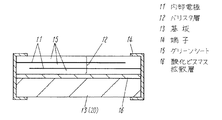
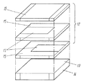
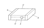
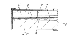
図1は本発明の一実施の形態における静電気対策部品の断面図、図2は同静電気対策部品の分解斜視図、図3は同静電気対策部品の斜視図である。 FIG. 1 is a cross-sectional view of an electrostatic countermeasure component according to an embodiment of the present invention, FIG. 2 is an exploded perspective view of the electrostatic countermeasure component, and FIG. 3 is a perspective view of the electrostatic countermeasure component.
図1〜図3において、本発明の一実施の形態における静電気対策部品は、複数の平面状の内部電極11を埋設したバリスタ層12と、このバリスタ層12を積層したアルミナを含有する基板13と、バリスタ層12の内部電極11に接続し、バリスタ層12の側面に形成した端子14とを備えている。
1 to 3, an antistatic component in one embodiment of the present invention includes a
バリスタ層12は、酸化亜鉛を主成分とし、少なくとも酸化ビスマスを添加物とするバリスタ材料の粉末を含有した未焼成のグリーンシート15を複数積層するとともに焼成して形成している。特に、バリスタ材料の粉末の平均粒径は0.5〜2.0μmとするとともに、酸化ビスマスの粉末の平均粒径は1.0μm以下としている。このグリーンシート15に銀等の材料からなる平面状の導電ペーストを積層すれば、バリスタ層12に内部電極11を埋設させることができる。
The
また、バリスタ層12と基板13とは焼結させてバリスタ層12の酸化ビスマスを基板13に拡散させ、基板13に酸化ビスマス拡散層16を形成している。バリスタ材料の粉末を含有した未焼成のグリーンシート15を焼成してバリスタ層12を形成することと、バリスタ層12と基板13との焼結は同時に行っている。この際、図4に示すように、基板13に含有されたアルミナ粒子の界面に酸化ビスマス粒子17が介在するように、酸化ビスマスは基板13に拡散される。基板13を低焼成温度セラミック基板(低温度で焼成可能な未焼成のセラミックシートを焼成して形成するもの)とすれば、低温度で焼成可能な未焼成のセラミックシートにバリスタ材料の粉末を含有した未焼成のグリーンシート15を積層し、これらを一般の温度よりも低い焼成温度で同時焼成して、バリスタ層12と基板13とを焼結させられるので、内部電極11として銀等の材料を用いても、熱に起因した悪影響を内部電極11に与えることもない。
Further, the
さらに、図5に示すように、バリスタ層12と基板13との焼結前には、バリスタ層12と基板13との間に接着層18を設けており、バリスタ層12と基板13との焼結の際に、この接着層18を介して酸化ビスマスを基板13に拡散させている。焼結後には、この接着層18は完全に消失する、または、その成分の一部が接着層18として残存する、または、その成分の一部がバリスタ層12または基板13に拡散している。バリスタ層12と基板13との界面近傍の成分組成分析グラフは図6に示すようになり、バリスタ層12には主成分の酸化亜鉛と酸化ビスマスが含有され、基板13には酸化ビスマスが拡散され、その含有量が多い部分に酸化ビスマス拡散層16が形成されている。
Further, as shown in FIG. 5, an
上記構成により、基板13にバリスタ層12を積層しているので、バリスタ層12の機械的強度が小さくても、基板13の機械的強度が付加されるため、薄型化を図ることができる。
With the above configuration, since the
特に、基板13はアルミナを含有するアルミナ基板20としているので、バリスタ層12の機械的強度よりもアルミナ基板20の機械的強度の方が大きくなり、バリスタ層12を非常に薄くするとともに、基板13そのものも非常に薄くしても、バリスタ層12に割れや欠けを発生することを抑制でき、薄型化をより図ることができる。
In particular, since the
また、基板13にバリスタ層12を積層しただけでは、バリスタ層12と基板13との剥離が生じ易いが、バリスタ層12は少なくとも酸化ビスマスを含有する材料からなり、このバリスタ層12と基板13とを焼結させて酸化ビスマスを基板13に拡散させ、基板13に酸化ビスマス拡散層16を設けているので、バリスタ層12と基板13とが一体的な物質となり、バリスタ層12と基板13との界面部分における剥離を防止することができる。
In addition, the
特に、バリスタ層12と基板13との間に接着層18を設けるとともに、この接着層18を介して酸化ビスマスを基板13に拡散させているので、酸化ビスマスがバリスタ層12から基板13に拡散される際、バリスタ層12と基板13との剥離が抑制された状態で酸化ビスマスが拡散されるので、拡散されやすく的確に基板13に酸化ビスマス拡散層16を形成して、バリスタ層12と基板13との剥離を防止することができる。
In particular, since the
さらに、バリスタ材料の粉末の平均粒径を0.5μm〜2.0μmとしているので、平均粒径が小さすぎてバリスタ材料の粉末を含有する未焼成のグリーンシート15を形成できなくなったり、平均粒径が大きすぎてグリーンシート15を焼成することができなくなったりすることを抑制できる。特に、酸化ビスマスの粉末の平均粒径を1.0μm以下とすることにより基板13へ拡散させやすく、より剥離を防止することができる。
Furthermore, since the average particle size of the varistor material powder is 0.5 μm to 2.0 μm, the average particle size is too small to form an unfired
なお、図7に示すように、基板13はガラスを含有するガラスセラミック層19をアルミナ基板20に積層し、バリスタ層12の酸化ビスマスをガラスセラミック層19に拡散させてガラスセラミック層19に酸化ビスマス拡散層16を形成するとともに、ガラスセラミック層19のガラスをアルミナ基板20に拡散させてアルミナ基板20にガラス拡散層21を形成してもよい。これにより、バリスタ層12とガラスセラミック層19とアルミナ基板20とが互いに剥離されにくくなり、特に、バリスタ層12はガラスセラミック層19と接触しているので、アルミナ基板20とバリスタ層12とが接触している場合に比べて、アルミナ基板20がバリスタ層12に与える影響が少なく、バリスタ特性の劣化を抑制できる。
As shown in FIG. 7, the
また、図8に示すように、ガラスセラミック層19とアルミナ基板20との間に接着層18を設けるとともに、接着層18を介してガラスをアルミナ基板20に拡散させてもよい。この場合、バリスタ層12と基板13との焼結の際に、この接着層18を介してガラスをアルミナ基板20に拡散させている。焼結後には、この接着層18は完全に消失する、または、その成分の一部が接着層18として残存する、または、その成分の一部がバリスタ層12またはアルミナ基板20に拡散している。これにより、ガラスがガラスセラミック層19からアルミナ基板20に拡散される際、ガラスセラミック層19とアルミナ基板20との剥離が抑制された状態でガラスが拡散されるので、拡散されやすく的確にアルミナ基板20にガラス拡散層21を形成して、ガラスセラミック層19とアルミナ基板20との剥離を防止することができる。
Further, as shown in FIG. 8, an
さらに、バリスタ層12の上面にガラスを含有するガラスセラミック層19を積層してもよく、これによれば、バリスタ層12の酸化ビスマスがバリスタ層12の表面から空気中に放散されることが抑制され、酸化ビスマスが基板13に拡散されやすくなり、バリスタ層12と基板13との剥離を防止しやすくなる。
Furthermore, a glass
このような静電気対策部品に別の抵抗やコイルやコンデンサ等からなる電子回路を形成してもよい。例えば、電子部品回路を形成した回路基板を本発明の基板として用いたり、バリスタ層12を積層した側と反対側の基板13の面に、電子部品回路を形成した回路層を積層したりしてもよい。電子部品回路は、薄膜形成等で形成すれば薄型化も可能である。
An electronic circuit composed of another resistor, a coil, a capacitor, or the like may be formed on such an anti-static component. For example, a circuit board on which an electronic component circuit is formed is used as a substrate of the present invention, or a circuit layer on which an electronic component circuit is formed is laminated on the surface of the
以上のように本発明にかかる静電気対策部品は、微小サージ電圧に対するバリスタ特性を保持しつつ、薄型化を図ることができるので、各種電子機器等に適用できる。 As described above, the anti-static component according to the present invention can be reduced in thickness while maintaining the varistor characteristics against a minute surge voltage, and thus can be applied to various electronic devices.
11 内部電極
12 バリスタ層
13 基板
14 端子
15 グリーンシート
16 酸化ビスマス拡散層
17 酸化ビスマス粒子
18 接着層
19 ガラスセラミック層
20 アルミナ基板
21 ガラス拡散層
DESCRIPTION OF
Claims (12)
Priority Applications (5)
| Application Number | Priority Date | Filing Date | Title |
|---|---|---|---|
| JP2004109779A JP4432586B2 (en) | 2004-04-02 | 2004-04-02 | Antistatic parts |
| EP05727186A EP1715494A4 (en) | 2004-04-02 | 2005-03-24 | COMPONENT WITH COUNTERMEASURE AGAINST STATIC ELECTRICITY |
| CN2005800119448A CN1942981B (en) | 2004-04-02 | 2005-03-24 | Antistatic Parts |
| US10/591,255 US7864025B2 (en) | 2004-04-02 | 2005-03-24 | Component with countermeasure to static electricity |
| PCT/JP2005/005322 WO2005098877A1 (en) | 2004-04-02 | 2005-03-24 | Component with countermeasure to static electricity |
Applications Claiming Priority (1)
| Application Number | Priority Date | Filing Date | Title |
|---|---|---|---|
| JP2004109779A JP4432586B2 (en) | 2004-04-02 | 2004-04-02 | Antistatic parts |
Publications (2)
| Publication Number | Publication Date |
|---|---|
| JP2005294673A true JP2005294673A (en) | 2005-10-20 |
| JP4432586B2 JP4432586B2 (en) | 2010-03-17 |
Family
ID=35125337
Family Applications (1)
| Application Number | Title | Priority Date | Filing Date |
|---|---|---|---|
| JP2004109779A Expired - Fee Related JP4432586B2 (en) | 2004-04-02 | 2004-04-02 | Antistatic parts |
Country Status (5)
| Country | Link |
|---|---|
| US (1) | US7864025B2 (en) |
| EP (1) | EP1715494A4 (en) |
| JP (1) | JP4432586B2 (en) |
| CN (1) | CN1942981B (en) |
| WO (1) | WO2005098877A1 (en) |
Cited By (5)
| Publication number | Priority date | Publication date | Assignee | Title |
|---|---|---|---|---|
| WO2007105865A1 (en) * | 2006-03-10 | 2007-09-20 | Joinset Co., Ltd | Ceramic component element and ceramic component and method for the same |
| US7741949B2 (en) | 2005-03-25 | 2010-06-22 | Panasonic Corporation | Varistor |
| EP1858033A4 (en) * | 2005-04-01 | 2013-10-09 | Panasonic Corp | VARISTOR AND ELECTRONIC COMPONENT MODULE USING THE SAME |
| WO2014035143A1 (en) * | 2012-08-28 | 2014-03-06 | ㈜ 아모엘이디 | Non-shrink varistor substrate and production method for same |
| US9391053B2 (en) | 2012-08-28 | 2016-07-12 | Amosense Co., Ltd. | Non-shrink varistor substrate and production method for same |
Families Citing this family (6)
| Publication number | Priority date | Publication date | Assignee | Title |
|---|---|---|---|---|
| US7741948B2 (en) * | 2006-10-02 | 2010-06-22 | Inpaq Technology Co., Ltd. | Laminated variable resistor |
| US8508325B2 (en) | 2010-12-06 | 2013-08-13 | Tdk Corporation | Chip varistor and chip varistor manufacturing method |
| JP5799672B2 (en) * | 2011-08-29 | 2015-10-28 | Tdk株式会社 | Chip varistor |
| JP5696623B2 (en) * | 2011-08-29 | 2015-04-08 | Tdk株式会社 | Chip varistor |
| KR101309326B1 (en) | 2012-05-30 | 2013-09-16 | 삼성전기주식회사 | Laminated chip electronic component, board for mounting the same, packing unit thereof |
| KR101309479B1 (en) | 2012-05-30 | 2013-09-23 | 삼성전기주식회사 | Laminated chip electronic component, board for mounting the same, packing unit thereof |
Family Cites Families (16)
| Publication number | Priority date | Publication date | Assignee | Title |
|---|---|---|---|---|
| GB1346851A (en) * | 1971-05-21 | 1974-02-13 | Matsushita Electric Industrial Co Ltd | Varistors |
| DE2735484C2 (en) * | 1977-08-05 | 1984-06-07 | Siemens AG, 1000 Berlin und 8000 München | Process for the production of thick film varistors with zinc oxide as the main component |
| JPS5810842B2 (en) | 1978-12-05 | 1983-02-28 | 松下電器産業株式会社 | Manufacturing method of thick film varistor |
| JPS5577103A (en) | 1978-12-05 | 1980-06-10 | Matsushita Electric Industrial Co Ltd | Method of fabricating thick varistor |
| JPS57184207A (en) | 1981-05-08 | 1982-11-12 | Matsushita Electric Industrial Co Ltd | Thick film varistor |
| JPS5885502A (en) | 1981-11-17 | 1983-05-21 | 松下電器産業株式会社 | Method of producing thick film varistor |
| JPS63316405A (en) * | 1987-06-18 | 1988-12-23 | Matsushita Electric Ind Co Ltd | Thick-film varistor |
| CN1034370A (en) | 1988-01-22 | 1989-08-02 | 上海科技大学 | The method of synthesizing aqueous gel materials by electron beam radiation |
| WO1993017438A1 (en) | 1992-02-25 | 1993-09-02 | Matsushita Electric Industrial Co., Ltd. | Zinc oxide varistor and production thereof |
| JP2970191B2 (en) * | 1992-03-27 | 1999-11-02 | 松下電器産業株式会社 | Electrode material for zinc oxide varistor |
| JP3453857B2 (en) | 1994-07-20 | 2003-10-06 | 松下電器産業株式会社 | Manufacturing method of multilayer varistor |
| TW394961B (en) * | 1997-03-20 | 2000-06-21 | Ceratech Corp | Low capacitance chip varistor and fabrication method thereof |
| JP3832071B2 (en) | 1998-02-10 | 2006-10-11 | 株式会社村田製作所 | Multilayer varistor |
| JPH11251152A (en) | 1998-03-03 | 1999-09-17 | Matsushita Electric Ind Co Ltd | Composite part and method of manufacturing the same |
| JP2001326108A (en) | 2000-05-18 | 2001-11-22 | Mitsubishi Electric Corp | Voltage nonlinear resistor and method of manufacturing the same |
| CN1251250C (en) | 2001-04-05 | 2006-04-12 | 佳邦科技股份有限公司 | Materials for transient overvoltage protection components |
-
2004
- 2004-04-02 JP JP2004109779A patent/JP4432586B2/en not_active Expired - Fee Related
-
2005
- 2005-03-24 CN CN2005800119448A patent/CN1942981B/en not_active Expired - Fee Related
- 2005-03-24 WO PCT/JP2005/005322 patent/WO2005098877A1/en not_active Ceased
- 2005-03-24 EP EP05727186A patent/EP1715494A4/en not_active Withdrawn
- 2005-03-24 US US10/591,255 patent/US7864025B2/en not_active Expired - Fee Related
Cited By (6)
| Publication number | Priority date | Publication date | Assignee | Title |
|---|---|---|---|---|
| US7741949B2 (en) | 2005-03-25 | 2010-06-22 | Panasonic Corporation | Varistor |
| EP1858033A4 (en) * | 2005-04-01 | 2013-10-09 | Panasonic Corp | VARISTOR AND ELECTRONIC COMPONENT MODULE USING THE SAME |
| WO2007105865A1 (en) * | 2006-03-10 | 2007-09-20 | Joinset Co., Ltd | Ceramic component element and ceramic component and method for the same |
| JP2009529233A (en) * | 2006-03-10 | 2009-08-13 | ジョインセット カンパニー リミテッド | Ceramic component element, ceramic component and manufacturing method thereof |
| WO2014035143A1 (en) * | 2012-08-28 | 2014-03-06 | ㈜ 아모엘이디 | Non-shrink varistor substrate and production method for same |
| US9391053B2 (en) | 2012-08-28 | 2016-07-12 | Amosense Co., Ltd. | Non-shrink varistor substrate and production method for same |
Also Published As
| Publication number | Publication date |
|---|---|
| EP1715494A1 (en) | 2006-10-25 |
| CN1942981B (en) | 2010-05-05 |
| JP4432586B2 (en) | 2010-03-17 |
| US7864025B2 (en) | 2011-01-04 |
| US20070171025A1 (en) | 2007-07-26 |
| EP1715494A4 (en) | 2010-03-17 |
| WO2005098877A1 (en) | 2005-10-20 |
| CN1942981A (en) | 2007-04-04 |
Similar Documents
| Publication | Publication Date | Title |
|---|---|---|
| TWI437593B (en) | Ceramic electronic component and method for manufacturing the same | |
| US9378874B2 (en) | Ceramic electronic component | |
| CN102610387A (en) | Multilayer ceramic electronic component | |
| JP4432586B2 (en) | Antistatic parts | |
| JP7196732B2 (en) | Multilayer ceramic capacitor and method for manufacturing the same | |
| JP4432489B2 (en) | Manufacturing method of anti-static parts | |
| CN112397309B (en) | Multilayer capacitor and board having the same mounted thereon | |
| KR101958775B1 (en) | Complex protection device and electronic device having the same | |
| JP2000106322A (en) | Multilayer ceramic capacitors | |
| US7741949B2 (en) | Varistor | |
| JP2000012375A (en) | Laminated ceramic electronic component | |
| JPH11297508A (en) | Multilayer ceramic electronic components | |
| JP2004040023A (en) | Voltage nonlinear resistor element | |
| JP2006005800A (en) | Piezoelectric speaker | |
| JP2008270391A (en) | Multilayer chip varistor and manufacturing method thereof | |
| JP5760894B2 (en) | ESD protection element | |
| JP2006196818A (en) | Multilayer ceramic parts | |
| JP2000331805A (en) | Multilayer ceramic array | |
| JP2006313877A (en) | Antistatic parts | |
| JP2006186039A (en) | Lamination type varistor | |
| WO2024241888A1 (en) | Method for producing multilayer ceramic electronic component | |
| JP2024045288A (en) | Multilayer varistor and method for manufacturing multilayer varistor | |
| JP2023144962A (en) | laminated ceramic parts | |
| JP2000331832A (en) | Laminate type impedance element | |
| JP2002217038A (en) | Ceramic electronic components |
Legal Events
| Date | Code | Title | Description |
|---|---|---|---|
| A621 | Written request for application examination |
Free format text: JAPANESE INTERMEDIATE CODE: A621 Effective date: 20070227 |
|
| RD01 | Notification of change of attorney |
Free format text: JAPANESE INTERMEDIATE CODE: A7421 Effective date: 20070313 |
|
| RD01 | Notification of change of attorney |
Free format text: JAPANESE INTERMEDIATE CODE: A7421 Effective date: 20091120 |
|
| TRDD | Decision of grant or rejection written | ||
| A01 | Written decision to grant a patent or to grant a registration (utility model) |
Free format text: JAPANESE INTERMEDIATE CODE: A01 Effective date: 20091201 |
|
| A01 | Written decision to grant a patent or to grant a registration (utility model) |
Free format text: JAPANESE INTERMEDIATE CODE: A01 |
|
| A61 | First payment of annual fees (during grant procedure) |
Free format text: JAPANESE INTERMEDIATE CODE: A61 Effective date: 20091214 |
|
| R151 | Written notification of patent or utility model registration |
Ref document number: 4432586 Country of ref document: JP Free format text: JAPANESE INTERMEDIATE CODE: R151 |
|
| FPAY | Renewal fee payment (event date is renewal date of database) |
Free format text: PAYMENT UNTIL: 20130108 Year of fee payment: 3 |
|
| FPAY | Renewal fee payment (event date is renewal date of database) |
Free format text: PAYMENT UNTIL: 20130108 Year of fee payment: 3 |
|
| LAPS | Cancellation because of no payment of annual fees |