JP2005294522A - Electrolytic capacitor and its manufacturing method - Google Patents
Electrolytic capacitor and its manufacturing method Download PDFInfo
- Publication number
- JP2005294522A JP2005294522A JP2004107215A JP2004107215A JP2005294522A JP 2005294522 A JP2005294522 A JP 2005294522A JP 2004107215 A JP2004107215 A JP 2004107215A JP 2004107215 A JP2004107215 A JP 2004107215A JP 2005294522 A JP2005294522 A JP 2005294522A
- Authority
- JP
- Japan
- Prior art keywords
- electrode layer
- electrolytic capacitor
- polymer
- layer
- particles
- Prior art date
- Legal status (The legal status is an assumption and is not a legal conclusion. Google has not performed a legal analysis and makes no representation as to the accuracy of the status listed.)
- Pending
Links
- 239000003990 capacitor Substances 0.000 title claims abstract description 207
- 238000004519 manufacturing process Methods 0.000 title claims abstract description 39
- 239000002245 particle Substances 0.000 claims abstract description 94
- 239000007784 solid electrolyte Substances 0.000 claims abstract description 46
- 239000002923 metal particle Substances 0.000 claims abstract description 44
- 239000000919 ceramic Substances 0.000 claims abstract description 40
- 238000000034 method Methods 0.000 claims abstract description 40
- 239000010410 layer Substances 0.000 claims description 360
- 229920000642 polymer Polymers 0.000 claims description 71
- 239000007788 liquid Substances 0.000 claims description 57
- 229910052751 metal Inorganic materials 0.000 claims description 44
- 239000002184 metal Substances 0.000 claims description 43
- 239000000463 material Substances 0.000 claims description 26
- PXHVJJICTQNCMI-UHFFFAOYSA-N Nickel Chemical compound [Ni] PXHVJJICTQNCMI-UHFFFAOYSA-N 0.000 claims description 25
- 229920001169 thermoplastic Polymers 0.000 claims description 19
- BASFCYQUMIYNBI-UHFFFAOYSA-N platinum Chemical compound [Pt] BASFCYQUMIYNBI-UHFFFAOYSA-N 0.000 claims description 18
- 239000010949 copper Substances 0.000 claims description 15
- BQCADISMDOOEFD-UHFFFAOYSA-N Silver Chemical compound [Ag] BQCADISMDOOEFD-UHFFFAOYSA-N 0.000 claims description 14
- 229910052709 silver Inorganic materials 0.000 claims description 14
- 239000004332 silver Substances 0.000 claims description 14
- 229910052782 aluminium Inorganic materials 0.000 claims description 13
- XAGFODPZIPBFFR-UHFFFAOYSA-N aluminium Chemical compound [Al] XAGFODPZIPBFFR-UHFFFAOYSA-N 0.000 claims description 13
- 229910052799 carbon Inorganic materials 0.000 claims description 12
- 239000010931 gold Substances 0.000 claims description 12
- OKTJSMMVPCPJKN-UHFFFAOYSA-N Carbon Chemical compound [C] OKTJSMMVPCPJKN-UHFFFAOYSA-N 0.000 claims description 11
- NRTOMJZYCJJWKI-UHFFFAOYSA-N Titanium nitride Chemical compound [Ti]#N NRTOMJZYCJJWKI-UHFFFAOYSA-N 0.000 claims description 10
- 229920001187 thermosetting polymer Polymers 0.000 claims description 10
- 239000004634 thermosetting polymer Substances 0.000 claims description 10
- RTAQQCXQSZGOHL-UHFFFAOYSA-N Titanium Chemical compound [Ti] RTAQQCXQSZGOHL-UHFFFAOYSA-N 0.000 claims description 9
- 239000010936 titanium Substances 0.000 claims description 9
- UONOETXJSWQNOL-UHFFFAOYSA-N tungsten carbide Chemical compound [W+]#[C-] UONOETXJSWQNOL-UHFFFAOYSA-N 0.000 claims description 9
- RYGMFSIKBFXOCR-UHFFFAOYSA-N Copper Chemical compound [Cu] RYGMFSIKBFXOCR-UHFFFAOYSA-N 0.000 claims description 8
- 229910052802 copper Inorganic materials 0.000 claims description 8
- 230000004044 response Effects 0.000 claims description 8
- 229910052719 titanium Inorganic materials 0.000 claims description 8
- XTDAIYZKROTZLD-UHFFFAOYSA-N boranylidynetantalum Chemical compound [Ta]#B XTDAIYZKROTZLD-UHFFFAOYSA-N 0.000 claims description 7
- ZOKXTWBITQBERF-UHFFFAOYSA-N Molybdenum Chemical compound [Mo] ZOKXTWBITQBERF-UHFFFAOYSA-N 0.000 claims description 6
- YXTPWUNVHCYOSP-UHFFFAOYSA-N bis($l^{2}-silanylidene)molybdenum Chemical compound [Si]=[Mo]=[Si] YXTPWUNVHCYOSP-UHFFFAOYSA-N 0.000 claims description 6
- 239000010941 cobalt Substances 0.000 claims description 6
- 229910017052 cobalt Inorganic materials 0.000 claims description 6
- GUTLYIVDDKVIGB-UHFFFAOYSA-N cobalt atom Chemical compound [Co] GUTLYIVDDKVIGB-UHFFFAOYSA-N 0.000 claims description 6
- PCHJSUWPFVWCPO-UHFFFAOYSA-N gold Chemical compound [Au] PCHJSUWPFVWCPO-UHFFFAOYSA-N 0.000 claims description 6
- 229910052737 gold Inorganic materials 0.000 claims description 6
- 229910052750 molybdenum Inorganic materials 0.000 claims description 6
- 239000011733 molybdenum Substances 0.000 claims description 6
- 229910052759 nickel Inorganic materials 0.000 claims description 6
- 229910052697 platinum Inorganic materials 0.000 claims description 6
- JBQYATWDVHIOAR-UHFFFAOYSA-N tellanylidenegermanium Chemical compound [Te]=[Ge] JBQYATWDVHIOAR-UHFFFAOYSA-N 0.000 claims description 6
- WFKWXMTUELFFGS-UHFFFAOYSA-N tungsten Chemical compound [W] WFKWXMTUELFFGS-UHFFFAOYSA-N 0.000 claims description 6
- 229910052721 tungsten Inorganic materials 0.000 claims description 6
- 239000010937 tungsten Substances 0.000 claims description 6
- ZVWKZXLXHLZXLS-UHFFFAOYSA-N zirconium nitride Chemical compound [Zr]#N ZVWKZXLXHLZXLS-UHFFFAOYSA-N 0.000 claims description 6
- 239000002344 surface layer Substances 0.000 claims description 5
- 238000007743 anodising Methods 0.000 claims description 4
- 239000002356 single layer Substances 0.000 claims description 3
- 230000000630 rising effect Effects 0.000 claims description 2
- 238000005868 electrolysis reaction Methods 0.000 claims 1
- 230000020169 heat generation Effects 0.000 abstract description 11
- 230000006378 damage Effects 0.000 abstract description 8
- 230000006870 function Effects 0.000 description 99
- 229920001940 conductive polymer Polymers 0.000 description 36
- 239000007787 solid Substances 0.000 description 30
- 239000000178 monomer Substances 0.000 description 26
- 230000000052 comparative effect Effects 0.000 description 22
- -1 polyethylenedioxy Polymers 0.000 description 22
- 239000000243 solution Substances 0.000 description 20
- 239000002019 doping agent Substances 0.000 description 16
- 239000002904 solvent Substances 0.000 description 13
- 239000007800 oxidant agent Substances 0.000 description 11
- 239000003822 epoxy resin Substances 0.000 description 10
- 239000011888 foil Substances 0.000 description 10
- 229920000647 polyepoxide Polymers 0.000 description 10
- 230000008569 process Effects 0.000 description 10
- 229920005989 resin Polymers 0.000 description 10
- 239000011347 resin Substances 0.000 description 10
- 239000002033 PVDF binder Substances 0.000 description 9
- 229920002981 polyvinylidene fluoride Polymers 0.000 description 9
- 230000007246 mechanism Effects 0.000 description 8
- 230000001590 oxidative effect Effects 0.000 description 8
- 238000012360 testing method Methods 0.000 description 8
- 238000010438 heat treatment Methods 0.000 description 7
- 230000007423 decrease Effects 0.000 description 6
- 239000003792 electrolyte Substances 0.000 description 6
- 229920006254 polymer film Polymers 0.000 description 6
- 239000000126 substance Substances 0.000 description 6
- 230000009471 action Effects 0.000 description 5
- 230000008859 change Effects 0.000 description 5
- 238000006243 chemical reaction Methods 0.000 description 5
- 238000000576 coating method Methods 0.000 description 5
- 150000003839 salts Chemical class 0.000 description 5
- CSCPPACGZOOCGX-UHFFFAOYSA-N Acetone Chemical compound CC(C)=O CSCPPACGZOOCGX-UHFFFAOYSA-N 0.000 description 4
- LRHPLDYGYMQRHN-UHFFFAOYSA-N N-Butanol Chemical compound CCCCO LRHPLDYGYMQRHN-UHFFFAOYSA-N 0.000 description 4
- NBIIXXVUZAFLBC-UHFFFAOYSA-N Phosphoric acid Chemical compound OP(O)(O)=O NBIIXXVUZAFLBC-UHFFFAOYSA-N 0.000 description 4
- QAOWNCQODCNURD-UHFFFAOYSA-N Sulfuric acid Chemical compound OS(O)(=O)=O QAOWNCQODCNURD-UHFFFAOYSA-N 0.000 description 4
- YTPLMLYBLZKORZ-UHFFFAOYSA-N Thiophene Chemical compound C=1C=CSC=1 YTPLMLYBLZKORZ-UHFFFAOYSA-N 0.000 description 4
- 239000000853 adhesive Substances 0.000 description 4
- 230000001070 adhesive effect Effects 0.000 description 4
- 230000015572 biosynthetic process Effects 0.000 description 4
- 238000001723 curing Methods 0.000 description 4
- 230000000694 effects Effects 0.000 description 4
- 238000002844 melting Methods 0.000 description 4
- 230000008018 melting Effects 0.000 description 4
- 239000010955 niobium Substances 0.000 description 4
- 238000006116 polymerization reaction Methods 0.000 description 4
- 229920000123 polythiophene Polymers 0.000 description 4
- 238000007639 printing Methods 0.000 description 4
- 239000000779 smoke Substances 0.000 description 4
- 239000011734 sodium Substances 0.000 description 4
- 238000003756 stirring Methods 0.000 description 4
- MTPVUVINMAGMJL-UHFFFAOYSA-N trimethyl(1,1,2,2,2-pentafluoroethyl)silane Chemical compound C[Si](C)(C)C(F)(F)C(F)(F)F MTPVUVINMAGMJL-UHFFFAOYSA-N 0.000 description 4
- XLYOFNOQVPJJNP-UHFFFAOYSA-N water Substances O XLYOFNOQVPJJNP-UHFFFAOYSA-N 0.000 description 4
- 239000004593 Epoxy Substances 0.000 description 3
- LFQSCWFLJHTTHZ-UHFFFAOYSA-N Ethanol Chemical compound CCO LFQSCWFLJHTTHZ-UHFFFAOYSA-N 0.000 description 3
- XEEYBQQBJWHFJM-UHFFFAOYSA-N Iron Chemical compound [Fe] XEEYBQQBJWHFJM-UHFFFAOYSA-N 0.000 description 3
- YXFVVABEGXRONW-UHFFFAOYSA-N Toluene Chemical compound CC1=CC=CC=C1 YXFVVABEGXRONW-UHFFFAOYSA-N 0.000 description 3
- 239000002253 acid Substances 0.000 description 3
- 239000000654 additive Substances 0.000 description 3
- 230000000996 additive effect Effects 0.000 description 3
- 239000002585 base Substances 0.000 description 3
- 239000006229 carbon black Substances 0.000 description 3
- 239000000460 chlorine Substances 0.000 description 3
- 238000007598 dipping method Methods 0.000 description 3
- 230000005484 gravity Effects 0.000 description 3
- 238000005304 joining Methods 0.000 description 3
- 230000004048 modification Effects 0.000 description 3
- 238000012986 modification Methods 0.000 description 3
- VLKZOEOYAKHREP-UHFFFAOYSA-N n-Hexane Chemical compound CCCCCC VLKZOEOYAKHREP-UHFFFAOYSA-N 0.000 description 3
- 229910052758 niobium Inorganic materials 0.000 description 3
- GUCVJGMIXFAOAE-UHFFFAOYSA-N niobium atom Chemical compound [Nb] GUCVJGMIXFAOAE-UHFFFAOYSA-N 0.000 description 3
- TWNQGVIAIRXVLR-UHFFFAOYSA-N oxo(oxoalumanyloxy)alumane Chemical compound O=[Al]O[Al]=O TWNQGVIAIRXVLR-UHFFFAOYSA-N 0.000 description 3
- 238000007747 plating Methods 0.000 description 3
- 229920000573 polyethylene Polymers 0.000 description 3
- 239000011148 porous material Substances 0.000 description 3
- 229910052715 tantalum Inorganic materials 0.000 description 3
- GUVRBAGPIYLISA-UHFFFAOYSA-N tantalum atom Chemical compound [Ta] GUVRBAGPIYLISA-UHFFFAOYSA-N 0.000 description 3
- GKWLILHTTGWKLQ-UHFFFAOYSA-N 2,3-dihydrothieno[3,4-b][1,4]dioxine Chemical compound O1CCOC2=CSC=C21 GKWLILHTTGWKLQ-UHFFFAOYSA-N 0.000 description 2
- FLDCSPABIQBYKP-UHFFFAOYSA-N 5-chloro-1,2-dimethylbenzimidazole Chemical compound ClC1=CC=C2N(C)C(C)=NC2=C1 FLDCSPABIQBYKP-UHFFFAOYSA-N 0.000 description 2
- ZCYVEMRRCGMTRW-UHFFFAOYSA-N 7553-56-2 Chemical compound [I] ZCYVEMRRCGMTRW-UHFFFAOYSA-N 0.000 description 2
- 239000001741 Ammonium adipate Substances 0.000 description 2
- PAYRUJLWNCNPSJ-UHFFFAOYSA-N Aniline Chemical compound NC1=CC=CC=C1 PAYRUJLWNCNPSJ-UHFFFAOYSA-N 0.000 description 2
- WKBOTKDWSSQWDR-UHFFFAOYSA-N Bromine atom Chemical compound [Br] WKBOTKDWSSQWDR-UHFFFAOYSA-N 0.000 description 2
- YLQBMQCUIZJEEH-UHFFFAOYSA-N Furan Chemical compound C=1C=COC=1 YLQBMQCUIZJEEH-UHFFFAOYSA-N 0.000 description 2
- DGAQECJNVWCQMB-PUAWFVPOSA-M Ilexoside XXIX Chemical compound C[C@@H]1CC[C@@]2(CC[C@@]3(C(=CC[C@H]4[C@]3(CC[C@@H]5[C@@]4(CC[C@@H](C5(C)C)OS(=O)(=O)[O-])C)C)[C@@H]2[C@]1(C)O)C)C(=O)O[C@H]6[C@@H]([C@H]([C@@H]([C@H](O6)CO)O)O)O.[Na+] DGAQECJNVWCQMB-PUAWFVPOSA-M 0.000 description 2
- SECXISVLQFMRJM-UHFFFAOYSA-N N-Methylpyrrolidone Chemical compound CN1CCCC1=O SECXISVLQFMRJM-UHFFFAOYSA-N 0.000 description 2
- UFWIBTONFRDIAS-UHFFFAOYSA-N Naphthalene Chemical compound C1=CC=CC2=CC=CC=C21 UFWIBTONFRDIAS-UHFFFAOYSA-N 0.000 description 2
- 229920001609 Poly(3,4-ethylenedioxythiophene) Polymers 0.000 description 2
- 239000004698 Polyethylene Substances 0.000 description 2
- KAESVJOAVNADME-UHFFFAOYSA-N Pyrrole Chemical compound C=1C=CNC=1 KAESVJOAVNADME-UHFFFAOYSA-N 0.000 description 2
- 150000007513 acids Chemical class 0.000 description 2
- 150000004996 alkyl benzenes Chemical class 0.000 description 2
- HSFWRNGVRCDJHI-UHFFFAOYSA-N alpha-acetylene Natural products C#C HSFWRNGVRCDJHI-UHFFFAOYSA-N 0.000 description 2
- 229910000147 aluminium phosphate Inorganic materials 0.000 description 2
- 235000019293 ammonium adipate Nutrition 0.000 description 2
- MWPLVEDNUUSJAV-UHFFFAOYSA-N anthracene Chemical compound C1=CC=CC2=CC3=CC=CC=C3C=C21 MWPLVEDNUUSJAV-UHFFFAOYSA-N 0.000 description 2
- 239000007864 aqueous solution Substances 0.000 description 2
- CUFNKYGDVFVPHO-UHFFFAOYSA-N azulene Chemical compound C1=CC=CC2=CC=CC2=C1 CUFNKYGDVFVPHO-UHFFFAOYSA-N 0.000 description 2
- GDTBXPJZTBHREO-UHFFFAOYSA-N bromine Substances BrBr GDTBXPJZTBHREO-UHFFFAOYSA-N 0.000 description 2
- 229910052794 bromium Inorganic materials 0.000 description 2
- 239000011575 calcium Substances 0.000 description 2
- 239000011248 coating agent Substances 0.000 description 2
- 238000001816 cooling Methods 0.000 description 2
- 238000005520 cutting process Methods 0.000 description 2
- 239000012153 distilled water Substances 0.000 description 2
- VYFYYTLLBUKUHU-UHFFFAOYSA-N dopamine Chemical group NCCC1=CC=C(O)C(O)=C1 VYFYYTLLBUKUHU-UHFFFAOYSA-N 0.000 description 2
- 238000001035 drying Methods 0.000 description 2
- 238000005516 engineering process Methods 0.000 description 2
- 125000005678 ethenylene group Chemical group [H]C([*:1])=C([H])[*:2] 0.000 description 2
- 238000001704 evaporation Methods 0.000 description 2
- 230000008020 evaporation Effects 0.000 description 2
- 239000012530 fluid Substances 0.000 description 2
- 229910052736 halogen Inorganic materials 0.000 description 2
- 150000002367 halogens Chemical class 0.000 description 2
- 229920001903 high density polyethylene Polymers 0.000 description 2
- 239000004700 high-density polyethylene Substances 0.000 description 2
- 239000005457 ice water Substances 0.000 description 2
- 239000011630 iodine Substances 0.000 description 2
- 229910052740 iodine Inorganic materials 0.000 description 2
- NPURPEXKKDAKIH-UHFFFAOYSA-N iodoimino(oxo)methane Chemical compound IN=C=O NPURPEXKKDAKIH-UHFFFAOYSA-N 0.000 description 2
- NUJOXMJBOLGQSY-UHFFFAOYSA-N manganese dioxide Chemical compound O=[Mn]=O NUJOXMJBOLGQSY-UHFFFAOYSA-N 0.000 description 2
- 150000002739 metals Chemical class 0.000 description 2
- 238000007254 oxidation reaction Methods 0.000 description 2
- VLTRZXGMWDSKGL-UHFFFAOYSA-M perchlorate Inorganic materials [O-]Cl(=O)(=O)=O VLTRZXGMWDSKGL-UHFFFAOYSA-M 0.000 description 2
- 229920000767 polyaniline Polymers 0.000 description 2
- 229920000414 polyfuran Polymers 0.000 description 2
- 229920000128 polypyrrole Polymers 0.000 description 2
- BBEAQIROQSPTKN-UHFFFAOYSA-N pyrene Chemical compound C1=CC=C2C=CC3=CC=CC4=CC=C1C2=C43 BBEAQIROQSPTKN-UHFFFAOYSA-N 0.000 description 2
- 230000009257 reactivity Effects 0.000 description 2
- 229910052708 sodium Inorganic materials 0.000 description 2
- 239000011343 solid material Substances 0.000 description 2
- BDHFUVZGWQCTTF-UHFFFAOYSA-M sulfonate Chemical compound [O-]S(=O)=O BDHFUVZGWQCTTF-UHFFFAOYSA-M 0.000 description 2
- AKEJUJNQAAGONA-UHFFFAOYSA-N sulfur trioxide Chemical compound O=S(=O)=O AKEJUJNQAAGONA-UHFFFAOYSA-N 0.000 description 2
- 239000004416 thermosoftening plastic Substances 0.000 description 2
- 229930192474 thiophene Natural products 0.000 description 2
- 238000001291 vacuum drying Methods 0.000 description 2
- 238000005406 washing Methods 0.000 description 2
- BQCIDUSAKPWEOX-UHFFFAOYSA-N 1,1-Difluoroethene Chemical compound FC(F)=C BQCIDUSAKPWEOX-UHFFFAOYSA-N 0.000 description 1
- 125000001140 1,4-phenylene group Chemical group [H]C1=C([H])C([*:2])=C([H])C([H])=C1[*:1] 0.000 description 1
- LCPVQAHEFVXVKT-UHFFFAOYSA-N 2-(2,4-difluorophenoxy)pyridin-3-amine Chemical compound NC1=CC=CN=C1OC1=CC=C(F)C=C1F LCPVQAHEFVXVKT-UHFFFAOYSA-N 0.000 description 1
- LYTMVABTDYMBQK-UHFFFAOYSA-N 2-benzothiophene Chemical compound C1=CC=CC2=CSC=C21 LYTMVABTDYMBQK-UHFFFAOYSA-N 0.000 description 1
- OMIHGPLIXGGMJB-UHFFFAOYSA-N 7-oxabicyclo[4.1.0]hepta-1,3,5-triene Chemical compound C1=CC=C2OC2=C1 OMIHGPLIXGGMJB-UHFFFAOYSA-N 0.000 description 1
- ODPYDILFQYARBK-UHFFFAOYSA-N 7-thiabicyclo[4.1.0]hepta-1,3,5-triene Chemical compound C1=CC=C2SC2=C1 ODPYDILFQYARBK-UHFFFAOYSA-N 0.000 description 1
- 229910018072 Al 2 O 3 Inorganic materials 0.000 description 1
- QGZKDVFQNNGYKY-UHFFFAOYSA-O Ammonium Chemical compound [NH4+] QGZKDVFQNNGYKY-UHFFFAOYSA-O 0.000 description 1
- 239000004254 Ammonium phosphate Substances 0.000 description 1
- 229910015900 BF3 Inorganic materials 0.000 description 1
- LSNNMFCWUKXFEE-UHFFFAOYSA-M Bisulfite Chemical compound OS([O-])=O LSNNMFCWUKXFEE-UHFFFAOYSA-M 0.000 description 1
- CPELXLSAUQHCOX-UHFFFAOYSA-M Bromide Chemical compound [Br-] CPELXLSAUQHCOX-UHFFFAOYSA-M 0.000 description 1
- OYPRJOBELJOOCE-UHFFFAOYSA-N Calcium Chemical compound [Ca] OYPRJOBELJOOCE-UHFFFAOYSA-N 0.000 description 1
- VEXZGXHMUGYJMC-UHFFFAOYSA-M Chloride anion Chemical compound [Cl-] VEXZGXHMUGYJMC-UHFFFAOYSA-M 0.000 description 1
- ZAMOUSCENKQFHK-UHFFFAOYSA-N Chlorine atom Chemical compound [Cl] ZAMOUSCENKQFHK-UHFFFAOYSA-N 0.000 description 1
- 229910020366 ClO 4 Inorganic materials 0.000 description 1
- XPIIDKFHGDPTIY-UHFFFAOYSA-N F.F.F.P Chemical compound F.F.F.P XPIIDKFHGDPTIY-UHFFFAOYSA-N 0.000 description 1
- VTLYFUHAOXGGBS-UHFFFAOYSA-N Fe3+ Chemical compound [Fe+3] VTLYFUHAOXGGBS-UHFFFAOYSA-N 0.000 description 1
- KRHYYFGTRYWZRS-UHFFFAOYSA-N Fluorane Chemical compound F KRHYYFGTRYWZRS-UHFFFAOYSA-N 0.000 description 1
- PXGOKWXKJXAPGV-UHFFFAOYSA-N Fluorine Chemical compound FF PXGOKWXKJXAPGV-UHFFFAOYSA-N 0.000 description 1
- VEXZGXHMUGYJMC-UHFFFAOYSA-N Hydrochloric acid Chemical compound Cl VEXZGXHMUGYJMC-UHFFFAOYSA-N 0.000 description 1
- MHAJPDPJQMAIIY-UHFFFAOYSA-N Hydrogen peroxide Chemical compound OO MHAJPDPJQMAIIY-UHFFFAOYSA-N 0.000 description 1
- 229920006370 Kynar Polymers 0.000 description 1
- 239000002841 Lewis acid Substances 0.000 description 1
- WHXSMMKQMYFTQS-UHFFFAOYSA-N Lithium Chemical compound [Li] WHXSMMKQMYFTQS-UHFFFAOYSA-N 0.000 description 1
- 229910016006 MoSi Inorganic materials 0.000 description 1
- GRYLNZFGIOXLOG-UHFFFAOYSA-N Nitric acid Chemical compound O[N+]([O-])=O GRYLNZFGIOXLOG-UHFFFAOYSA-N 0.000 description 1
- 239000004721 Polyphenylene oxide Substances 0.000 description 1
- 239000004734 Polyphenylene sulfide Substances 0.000 description 1
- ZLMJMSJWJFRBEC-UHFFFAOYSA-N Potassium Chemical compound [K] ZLMJMSJWJFRBEC-UHFFFAOYSA-N 0.000 description 1
- XUIMIQQOPSSXEZ-UHFFFAOYSA-N Silicon Chemical compound [Si] XUIMIQQOPSSXEZ-UHFFFAOYSA-N 0.000 description 1
- 229910007116 SnPb Inorganic materials 0.000 description 1
- ATJFFYVFTNAWJD-UHFFFAOYSA-N Tin Chemical compound [Sn] ATJFFYVFTNAWJD-UHFFFAOYSA-N 0.000 description 1
- TWVGAEQMWFGWDX-UHFFFAOYSA-N acetylene;thiophene Chemical group C#C.C=1C=CSC=1 TWVGAEQMWFGWDX-UHFFFAOYSA-N 0.000 description 1
- 150000008065 acid anhydrides Chemical class 0.000 description 1
- 229910052783 alkali metal Inorganic materials 0.000 description 1
- 150000001340 alkali metals Chemical class 0.000 description 1
- 229910052784 alkaline earth metal Inorganic materials 0.000 description 1
- 150000001342 alkaline earth metals Chemical class 0.000 description 1
- 125000000217 alkyl group Chemical group 0.000 description 1
- 229910000148 ammonium phosphate Inorganic materials 0.000 description 1
- 235000019289 ammonium phosphates Nutrition 0.000 description 1
- 150000001450 anions Chemical class 0.000 description 1
- YBGKQGSCGDNZIB-UHFFFAOYSA-N arsenic pentafluoride Chemical compound F[As](F)(F)(F)F YBGKQGSCGDNZIB-UHFFFAOYSA-N 0.000 description 1
- JCMGUODNZMETBM-UHFFFAOYSA-N arsenic trifluoride Chemical compound F[As](F)F JCMGUODNZMETBM-UHFFFAOYSA-N 0.000 description 1
- 239000012752 auxiliary agent Substances 0.000 description 1
- 230000008901 benefit Effects 0.000 description 1
- WTEOIRVLGSZEPR-UHFFFAOYSA-N boron trifluoride Chemical compound FB(F)F WTEOIRVLGSZEPR-UHFFFAOYSA-N 0.000 description 1
- 239000007853 buffer solution Substances 0.000 description 1
- 229910052791 calcium Inorganic materials 0.000 description 1
- VZDYWEUILIUIDF-UHFFFAOYSA-J cerium(4+);disulfate Chemical compound [Ce+4].[O-]S([O-])(=O)=O.[O-]S([O-])(=O)=O VZDYWEUILIUIDF-UHFFFAOYSA-J 0.000 description 1
- 239000003795 chemical substances by application Substances 0.000 description 1
- 229910052801 chlorine Inorganic materials 0.000 description 1
- 238000002485 combustion reaction Methods 0.000 description 1
- 150000001875 compounds Chemical class 0.000 description 1
- 239000004020 conductor Substances 0.000 description 1
- 238000012790 confirmation Methods 0.000 description 1
- 229920000547 conjugated polymer Polymers 0.000 description 1
- 238000010276 construction Methods 0.000 description 1
- 230000008602 contraction Effects 0.000 description 1
- 238000007796 conventional method Methods 0.000 description 1
- 230000003247 decreasing effect Effects 0.000 description 1
- 230000007547 defect Effects 0.000 description 1
- 230000006866 deterioration Effects 0.000 description 1
- MNNHAPBLZZVQHP-UHFFFAOYSA-N diammonium hydrogen phosphate Chemical compound [NH4+].[NH4+].OP([O-])([O-])=O MNNHAPBLZZVQHP-UHFFFAOYSA-N 0.000 description 1
- 229960003638 dopamine Drugs 0.000 description 1
- 239000008151 electrolyte solution Substances 0.000 description 1
- 238000005530 etching Methods 0.000 description 1
- 125000002534 ethynyl group Chemical group [H]C#C* 0.000 description 1
- 238000010304 firing Methods 0.000 description 1
- GVEPBJHOBDJJJI-UHFFFAOYSA-N fluoranthrene Natural products C1=CC(C2=CC=CC=C22)=C3C2=CC=CC3=C1 GVEPBJHOBDJJJI-UHFFFAOYSA-N 0.000 description 1
- 229910052731 fluorine Inorganic materials 0.000 description 1
- 239000011737 fluorine Substances 0.000 description 1
- 239000011521 glass Substances 0.000 description 1
- 238000013007 heat curing Methods 0.000 description 1
- QWPPOHNGKGFGJK-UHFFFAOYSA-N hypochlorous acid Chemical compound ClO QWPPOHNGKGFGJK-UHFFFAOYSA-N 0.000 description 1
- 238000007654 immersion Methods 0.000 description 1
- 230000006872 improvement Effects 0.000 description 1
- XMBWDFGMSWQBCA-UHFFFAOYSA-M iodide Chemical compound [I-] XMBWDFGMSWQBCA-UHFFFAOYSA-M 0.000 description 1
- 229940006461 iodide ion Drugs 0.000 description 1
- 150000002500 ions Chemical class 0.000 description 1
- 229910052742 iron Inorganic materials 0.000 description 1
- RBTARNINKXHZNM-UHFFFAOYSA-K iron trichloride Chemical compound Cl[Fe](Cl)Cl RBTARNINKXHZNM-UHFFFAOYSA-K 0.000 description 1
- LQBJWKCYZGMFEV-UHFFFAOYSA-N lead tin Chemical compound [Sn].[Pb] LQBJWKCYZGMFEV-UHFFFAOYSA-N 0.000 description 1
- 150000007517 lewis acids Chemical class 0.000 description 1
- 239000011344 liquid material Substances 0.000 description 1
- 229910052744 lithium Inorganic materials 0.000 description 1
- 229910001507 metal halide Inorganic materials 0.000 description 1
- 150000005309 metal halides Chemical class 0.000 description 1
- 230000005012 migration Effects 0.000 description 1
- 238000013508 migration Methods 0.000 description 1
- 239000012046 mixed solvent Substances 0.000 description 1
- 239000000203 mixture Substances 0.000 description 1
- 229910021344 molybdenum silicide Inorganic materials 0.000 description 1
- PSZYNBSKGUBXEH-UHFFFAOYSA-M naphthalene-1-sulfonate Chemical compound C1=CC=C2C(S(=O)(=O)[O-])=CC=CC2=C1 PSZYNBSKGUBXEH-UHFFFAOYSA-M 0.000 description 1
- 229910017604 nitric acid Inorganic materials 0.000 description 1
- 239000012299 nitrogen atmosphere Substances 0.000 description 1
- 239000003921 oil Substances 0.000 description 1
- 150000007524 organic acids Chemical class 0.000 description 1
- 239000003960 organic solvent Substances 0.000 description 1
- 150000002927 oxygen compounds Chemical class 0.000 description 1
- VLTRZXGMWDSKGL-UHFFFAOYSA-N perchloric acid Chemical compound OCl(=O)(=O)=O VLTRZXGMWDSKGL-UHFFFAOYSA-N 0.000 description 1
- 150000002978 peroxides Chemical class 0.000 description 1
- JRKICGRDRMAZLK-UHFFFAOYSA-L persulfate group Chemical group S(=O)(=O)([O-])OOS(=O)(=O)[O-] JRKICGRDRMAZLK-UHFFFAOYSA-L 0.000 description 1
- WKFBZNUBXWCCHG-UHFFFAOYSA-N phosphorus trifluoride Chemical compound FP(F)F WKFBZNUBXWCCHG-UHFFFAOYSA-N 0.000 description 1
- 239000004033 plastic Substances 0.000 description 1
- 229920003023 plastic Polymers 0.000 description 1
- 229920000553 poly(phenylenevinylene) Polymers 0.000 description 1
- 229920001197 polyacetylene Polymers 0.000 description 1
- 229920000323 polyazulene Polymers 0.000 description 1
- 229920000417 polynaphthalene Polymers 0.000 description 1
- 229920006380 polyphenylene oxide Polymers 0.000 description 1
- 229920000069 polyphenylene sulfide Polymers 0.000 description 1
- 229910052700 potassium Inorganic materials 0.000 description 1
- 239000011591 potassium Substances 0.000 description 1
- 230000002265 prevention Effects 0.000 description 1
- 238000004080 punching Methods 0.000 description 1
- 238000011160 research Methods 0.000 description 1
- 238000007788 roughening Methods 0.000 description 1
- 238000007650 screen-printing Methods 0.000 description 1
- MABNMNVCOAICNO-UHFFFAOYSA-N selenophene Chemical compound C=1C=C[se]C=1 MABNMNVCOAICNO-UHFFFAOYSA-N 0.000 description 1
- 239000004065 semiconductor Substances 0.000 description 1
- 229910052710 silicon Inorganic materials 0.000 description 1
- 239000010703 silicon Substances 0.000 description 1
- CHQMHPLRPQMAMX-UHFFFAOYSA-L sodium persulfate Substances [Na+].[Na+].[O-]S(=O)(=O)OOS([O-])(=O)=O CHQMHPLRPQMAMX-UHFFFAOYSA-L 0.000 description 1
- KVCGISUBCHHTDD-UHFFFAOYSA-M sodium;4-methylbenzenesulfonate Chemical compound [Na+].CC1=CC=C(S([O-])(=O)=O)C=C1 KVCGISUBCHHTDD-UHFFFAOYSA-M 0.000 description 1
- 238000004528 spin coating Methods 0.000 description 1
- 239000007921 spray Substances 0.000 description 1
- 150000003467 sulfuric acid derivatives Chemical class 0.000 description 1
- TULWUZJYDBGXMY-UHFFFAOYSA-N tellurophene Chemical compound [Te]1C=CC=C1 TULWUZJYDBGXMY-UHFFFAOYSA-N 0.000 description 1
- XJDNKRIXUMDJCW-UHFFFAOYSA-J titanium tetrachloride Chemical compound Cl[Ti](Cl)(Cl)Cl XJDNKRIXUMDJCW-UHFFFAOYSA-J 0.000 description 1
- JOXIMZWYDAKGHI-UHFFFAOYSA-M toluene-4-sulfonate Chemical compound CC1=CC=C(S([O-])(=O)=O)C=C1 JOXIMZWYDAKGHI-UHFFFAOYSA-M 0.000 description 1
- JOXIMZWYDAKGHI-UHFFFAOYSA-N toluene-4-sulfonic acid Chemical compound CC1=CC=C(S(O)(=O)=O)C=C1 JOXIMZWYDAKGHI-UHFFFAOYSA-N 0.000 description 1
- 230000007704 transition Effects 0.000 description 1
- WYXIGTJNYDDFFH-UHFFFAOYSA-Q triazanium;borate Chemical compound [NH4+].[NH4+].[NH4+].[O-]B([O-])[O-] WYXIGTJNYDDFFH-UHFFFAOYSA-Q 0.000 description 1
- KBSJJSOGQSGFRD-UHFFFAOYSA-K trichlorotungsten Chemical compound Cl[W](Cl)Cl KBSJJSOGQSGFRD-UHFFFAOYSA-K 0.000 description 1
- 238000003466 welding Methods 0.000 description 1
Images
Landscapes
- Fixed Capacitors And Capacitor Manufacturing Machines (AREA)
Abstract
Description
本発明は、固体電解質層を備えた電解コンデンサおよびその製造方法に関する。 The present invention relates to an electrolytic capacitor including a solid electrolyte layer and a method for manufacturing the same.
近年、高周波用途に適した電子部品のうちの1つとして、多様な電子機器に電解コンデンサが搭載されている。この電解コンデンサに関しては、例えば、電子機器のデジタル化、小型化および高速化が加速的に進行している情勢下において、大容量化や低インピーダンス化が要望されていると共に、動作安定性や動作信頼性の確保、ならびに高寿命化も併せて要望されている。 In recent years, electrolytic capacitors are mounted on various electronic devices as one of electronic components suitable for high-frequency applications. With regard to this electrolytic capacitor, for example, in a situation where the digitization, downsizing and speeding up of electronic devices are accelerating, there is a demand for large capacity and low impedance, as well as operational stability and operation. There is also a demand for ensuring reliability and extending the service life.
電解コンデンサの主要部(コンデンサ素子)は、例えば、弁作用金属により構成された陽極と、この陽極の表層が陽極酸化されることにより形成された酸化皮膜(誘電体層)と、電解質層と、陰極とがこの順に積層された積層構造を有している。 The main part (capacitor element) of the electrolytic capacitor includes, for example, an anode made of a valve metal, an oxide film (dielectric layer) formed by anodizing the surface layer of the anode, an electrolyte layer, The cathode has a laminated structure in which the cathode is laminated in this order.
この電解コンデンサは、主に、電解質層の種類に応じて2種類に大別される。すなわち、液体材料により構成された電解質層(電解液)を含んでコンデンサ素子が構成され、主にイオン伝導性を利用した導電機構を有する液体電解コンデンサと、錯塩や導電性高分子などの固体材料により構成された電解質層(固体電解質層)を含んでコンデンサ素子が構成され、主に電子伝導性を利用した導電機構を有する固体電解コンデンサである。これらの2種類の電解コンデンサを作動特性の安定性の観点において比較すると、例えば、液体電解コンデンサでは電解液の漏洩や蒸発に起因して作動特性が経時劣化し得るのに対して、この電解液の漏洩や蒸発に起因する作動特性の経時劣化は固体電解コンデンサでは起こり得ないため、今後主流になり得る電解コンデンサとして、最近では液体電解コンデンサに代えて固体電解コンデンサに関する研究開発が活発に進められている。この固体電解コンデンサに関する研究過程では、例えば、漏れ電流特性、インピーダンス特性ならびに耐熱特性などの一連の作動特性を考慮して、固体電解質層の主要部が二酸化マンガンや錯塩から共役系の導電性高分子に急速に移行しつつある。 This electrolytic capacitor is mainly divided into two types according to the type of the electrolyte layer. That is, a capacitor element is formed including an electrolyte layer (electrolyte) made of a liquid material, and has a conductive mechanism mainly utilizing ion conductivity, and a solid material such as a complex salt or a conductive polymer The capacitor element is configured to include the electrolyte layer (solid electrolyte layer) configured by the above, and is a solid electrolytic capacitor having a conductive mechanism mainly utilizing electronic conductivity. When these two types of electrolytic capacitors are compared in terms of stability of operating characteristics, for example, in liquid electrolytic capacitors, the operating characteristics may deteriorate over time due to leakage or evaporation of the electrolytic solution. As the electrolytic capacitors that can become the mainstream in the future are recently being actively researched and developed for solid electrolytic capacitors instead of liquid electrolytic capacitors, the deterioration of the operating characteristics due to leakage and evaporation of the liquid cannot occur with solid electrolytic capacitors. ing. In this research process on solid electrolytic capacitors, for example, considering the series of operating characteristics such as leakage current characteristics, impedance characteristics, and heat resistance characteristics, the main part of the solid electrolyte layer is composed of manganese dioxide or complex salts and conjugated conductive polymers. Is moving rapidly.
この固体電解コンデンサに関しては、特に、以下で説明する技術的背景に基づき、短絡時の発熱に起因して破壊されること(発火や燃焼を含む)を防止するために、所定の温度範囲内において温度の上昇に応じて抵抗が上昇する機能(いわゆるPTC(Positive Temperature Coefficient)機能)が要望されている。 With respect to this solid electrolytic capacitor, in particular, based on the technical background described below, in order to prevent destruction (including ignition and combustion) due to heat generation at the time of a short circuit, within a predetermined temperature range There is a demand for a function (so-called PTC (Positive Temperature Coefficient) function) in which the resistance increases with an increase in temperature.
すなわち、固体電解コンデンサは、上記したように多様な電子機器(電子回路)に搭載されており、一般に故障率が低い点において利点を有している。ところが、例えば、電子回路上のトラブルに起因して固体電解コンデンサに過電圧(定格電圧よりも大きい電圧)や逆電圧(正負が逆の電圧)が印加された場合に、それらの過電圧や逆電圧に起因して誘電体層が部分的に破損すると、陽極と固体電解質層および陰極とが意図せずに導通するため、固体電解コンデンサが短絡してしまう。この短絡が発生した場合に、固体電解コンデンサに過電流(短絡電流)が流れると、その固体電解コンデンサが発熱し、場合によっては発熱に起因して発火または燃焼することにより破壊されてしまう。 That is, the solid electrolytic capacitor is mounted on various electronic devices (electronic circuits) as described above, and generally has an advantage in that the failure rate is low. However, for example, when an overvoltage (a voltage greater than the rated voltage) or a reverse voltage (a voltage that is opposite in positive and negative) is applied to the solid electrolytic capacitor due to a problem in the electronic circuit, the overvoltage or reverse voltage When the dielectric layer is partially damaged due to this, the anode, the solid electrolyte layer, and the cathode are unintentionally conducted, and the solid electrolytic capacitor is short-circuited. When this short circuit occurs, if an overcurrent (short circuit current) flows through the solid electrolytic capacitor, the solid electrolytic capacitor generates heat, and in some cases, the solid electrolytic capacitor is destroyed by firing or burning.
この固体電解コンデンサの短絡時の発熱に起因する破壊を防止すると共に、固体電解コンデンサと共に電子回路に搭載されている回路部品の破壊も併せて防止する対策としては、例えば、固体電解コンデンサにヒューズを搭載する技術が考えられる。このヒューズを搭載した固体電解コンデンサとしては、例えば、陰極と陰極リード(通電用のリード)とがヒューズを介して電気的に接続された構成を有するものが知られている。この種の固体電解コンデンサでは、短絡時の発熱に起因してヒューズが溶解切断されることにより回路機構が遮断され、すなわち過電流の電流経路が遮断されるため、固体電解コンデンサの破壊が防止される。ところが、ヒューズを利用した固体電解コンデンサでは、そのヒューズの構造的および機構的要因に起因していくつかの問題がある。第1に、固体電解コンデンサにヒューズを搭載すると、その固体電解コンデンサの構造が複雑化かつ大型化してしまう。第2に、ヒューズは機械的強度が弱く、すなわちヒューズは取り扱いが困難なため、固体電解コンデンサの製造工程が複雑化すると共に製造歩留まりが低下してしまう。第3に、ヒューズを搭載した固体電解コンデンサでは、場合によっては信頼性の観点において不安がある。具体的には、例えば、ヒューズの周囲がモールド樹脂で強固に覆われている場合には、短絡時の発熱に起因してヒューズが溶解したとしても、そのヒューズがモールド樹脂の存在に起因して完全に切断されない可能性があるため、依然として回路機構が遮断されない場合に固体電解コンデンサが破壊されるおそれがある。したがって、固体電解コンデンサの破壊防止に関する信頼性を高めるために、ヒューズに代わる安全機構が模索されており、その安全機構としてPTC機能が要望されているのである。 As a measure to prevent destruction due to heat generation at the time of short-circuiting of this solid electrolytic capacitor and also prevent destruction of circuit components mounted on the electronic circuit together with the solid electrolytic capacitor, for example, a fuse is attached to the solid electrolytic capacitor. The technology to be installed can be considered. As a solid electrolytic capacitor equipped with this fuse, for example, a capacitor having a configuration in which a cathode and a cathode lead (a lead for energization) are electrically connected via a fuse is known. In this type of solid electrolytic capacitor, the circuit mechanism is cut off by melting and cutting the fuse due to heat generation at the time of short circuit, that is, the overcurrent current path is cut off, so that destruction of the solid electrolytic capacitor is prevented. The However, a solid electrolytic capacitor using a fuse has several problems due to structural and mechanical factors of the fuse. First, when a fuse is mounted on a solid electrolytic capacitor, the structure of the solid electrolytic capacitor becomes complicated and large. Secondly, the fuse has a low mechanical strength, that is, the fuse is difficult to handle, which complicates the manufacturing process of the solid electrolytic capacitor and decreases the manufacturing yield. Thirdly, solid electrolytic capacitors equipped with fuses may be anxious in terms of reliability. Specifically, for example, when the periphery of the fuse is firmly covered with mold resin, even if the fuse is melted due to heat generation at the time of short circuit, the fuse is caused by the presence of mold resin. Since it may not be completely disconnected, the solid electrolytic capacitor may be destroyed if the circuit mechanism is still not interrupted. Therefore, in order to increase the reliability regarding prevention of destruction of the solid electrolytic capacitor, a safety mechanism replacing the fuse is being sought, and a PTC function is desired as the safety mechanism.
このPTC機能を有する電解コンデンサとしては、既にいくつかの態様を有するものが提案されている。具体的には、例えば、PTCサーミスタがコンデンサ素子に対向配置され、それらのPTCサーミスタおよびコンデンサ素子がモールド樹脂で覆われた構成を有するものが知られている(例えば、特許文献1参照。)。なお、この電解コンデンサでは、ヒューズに代わる安全機構としてPTCサーミスタが設けられているわけではない。また、例えば、コンデンサ素子の陽極(内部端子)と陽極リード(外部端子)とがPTCサーミスタ(半導体セラミック層)を介して電気的に接続された構成を有するものが知られている(例えば、特許文献2参照。)。さらに、例えば、コンデンサ素子の一方の電極(外部電極)と電極リード(金属端子)とがPTCサーミスタ(PTC機能を有する過電流・過熱保護素子)を介して電気的に接続された構成を有するものが知られている(例えば、特許文献3参照。)。
ところで、PTC機能を有する固体電解コンデンサの高性能化を図るためには、その固体電解コンデンサの抵抗特性を可能な限り低下させる必要がある。しかしながら、従来の電解コンデンサの製造方法では、PTCサーミスタに基づくPTC機能を利用することにより短絡時の発熱に起因する電解コンデンサの破壊は防止されるが、電解コンデンサの高性能化を図る上では抵抗特性の低さが未だ十分とは言えないため、その抵抗特性の観点において未だ改善の余地がある。したがって、PTC機能を利用して短絡時の発熱に起因する破壊を防止しつつ、固体電解コンデンサの高性能化を高めるためには、そのPTC機能を有する固体電解コンデンサの抵抗特性を可能な限り低下させることが可能な技術の確立が急務である。 Incidentally, in order to improve the performance of a solid electrolytic capacitor having a PTC function, it is necessary to reduce the resistance characteristics of the solid electrolytic capacitor as much as possible. However, in the conventional method of manufacturing an electrolytic capacitor, the use of the PTC function based on the PTC thermistor prevents the electrolytic capacitor from being destroyed due to heat generation at the time of a short circuit. Since the low characteristic is still not sufficient, there is still room for improvement in terms of the resistance characteristic. Therefore, in order to improve the performance of the solid electrolytic capacitor while preventing the damage caused by the heat generation at the time of short circuit using the PTC function, the resistance characteristic of the solid electrolytic capacitor having the PTC function is reduced as much as possible. There is an urgent need to establish technologies that can be used.
本発明はかかる問題点に鑑みてなされたもので、その第1の目的は、PTC機能を有する電解コンデンサの抵抗特性を可能な限り低下させることが可能な電解コンデンサの製造方法を提供することにある。 The present invention has been made in view of such problems, and a first object thereof is to provide an electrolytic capacitor manufacturing method capable of reducing resistance characteristics of an electrolytic capacitor having a PTC function as much as possible. is there.
また、本発明の第2の目的は、可能な限り低抵抗でPTC機能が確保された電解コンデンサを提供することにある。 A second object of the present invention is to provide an electrolytic capacitor having a PTC function as low resistance as possible.
本発明に係る電解コンデンサは、第1の電極層と、誘電体層と、固体電解質層と、金属粒子および導電性セラミック粒子のうちの少なくとも一方を含むと共に所定の温度範囲内において温度の上昇に伴って抵抗が上昇する第2の電極層とがこの順に積層された積層構造を有するものである。 An electrolytic capacitor according to the present invention includes a first electrode layer, a dielectric layer, a solid electrolyte layer, at least one of metal particles and conductive ceramic particles, and increases the temperature within a predetermined temperature range. Accordingly, the second electrode layer whose resistance increases is stacked in this order.
本発明に係る電解コンデンサでは、所定の温度範囲内において温度の上昇に応じて抵抗が上昇する機能(いわゆるPTC機能)が第2の電極層において確保されつつ、抵抗特性が低下する。 In the electrolytic capacitor according to the present invention, the function of increasing the resistance in response to the increase in temperature within a predetermined temperature range (so-called PTC function) is ensured in the second electrode layer, and the resistance characteristics are deteriorated.
本発明に係る電解コンデンサの製造方法は、第1の電極層、誘電体層および固体電解質層がこの順に積層された積層構造のうちの固体電解質層上に、金属粒子および導電性セラミック粒子のうちの少なくとも一方を含むと共に所定の温度範囲内において温度の上昇に応じて抵抗が上昇するように第2の電極層を形成したものである。 The method for producing an electrolytic capacitor according to the present invention includes a metal electrode and a conductive ceramic particle on a solid electrolyte layer of a laminated structure in which a first electrode layer, a dielectric layer, and a solid electrolyte layer are laminated in this order. And the second electrode layer is formed so that the resistance increases as the temperature rises within a predetermined temperature range.
本発明に係る電解コンデンサの製造方法では、所定の温度範囲内において温度の上昇に応じて抵抗が上昇する機能(いわゆるPTC機能)を有するように第2の電極層が形成される際に、金属粒子および導電性セラミック粒子のうちの少なくとも一方を含むように第2の電極層が形成される。これらの金属粒子または導電性セラミック粒子の低抵抗特性に基づいて電解コンデンサの抵抗特性が低下するため、PTC機能を利用して短絡時の発熱に起因する電解コンデンサの破壊を防止しつつ、その電解コンデンサの抵抗特性を低下させることが可能となる。 In the method for manufacturing an electrolytic capacitor according to the present invention, when the second electrode layer is formed so as to have a function of increasing resistance in response to an increase in temperature within a predetermined temperature range (so-called PTC function), a metal The second electrode layer is formed so as to include at least one of the particles and the conductive ceramic particles. Since the resistance characteristic of the electrolytic capacitor is lowered based on the low resistance characteristic of these metal particles or conductive ceramic particles, the electrolytic capacitor can be electrolyzed while preventing the destruction of the electrolytic capacitor due to heat generation at the time of short circuit by using the PTC function. It becomes possible to reduce the resistance characteristics of the capacitor.
特に、本発明に係る電解コンデンサでは、第2の電極層が、2層以上の層が積層された積層構造を有し、その2層以上の層のうちの少なくとも1つの層において金属粒子および導電性セラミック粒子のうちの少なくとも一方を含むと共に所定の温度範囲内において温度の上昇に伴って抵抗が上昇してもよいし、あるいは単層構造を有していてもよい。第2の電極層が積層構造を有する場合には、導電性を確保するための主電極層と、この主電極層と固体電解質層との間に配設され、主電極層を固体電解質層に電気的に接合させるための副電極層と、主電極層を挟んで副電極層と反対側に配設され、金属粒子および導電性セラミック粒子のうちの少なくとも一方を含むと共に所定の温度範囲内において温度の上昇に伴って抵抗が上昇する補助電極層とを含む3層構造を有し、主電極層が金属を含んで構成され、副電極層がカーボンを含んで構成されていてもよい。この場合には、金属粒子がニッケル(Ni)、銅(Cu)、アルミニウム(Al)、タングステン(W)、モリブデン(Mo)、亜鉛(Zn)、コバルト(Co)、白金(Pt)、金(Au)および銀(Ag)を含む群のうちの少なくとも1種であり、導電性セラミック粒子が炭化タングステン(WC)、窒化チタン(TiN)、窒化ジルコニウム(ZrN)、窒化チタン(TiN)、ホウ化チタン(TiB2 )、ケイ化モリブデン(MoSi2 )およびホウ化タンタル(TaB2 )を含む群のうちの少なくとも1種であるのが好ましい。また、所定の温度範囲内において温度の上昇に応じて抵抗を上昇させるための材料が金属粒子および導電性セラミック粒子のうちの少なくとも一方を含む液状高分子であり、第2の電極層が液状高分子が膜化されることにより形成された膜状高分子とその膜状高分子中に保持された金属粒子および導電性セラミック粒子のうちの少なくとも一方とを含んで構成されていてもよく、この場合には、液状高分子が熱硬化性高分子および可溶性熱可塑性高分子のうちの少なくとも一方を含んでいるのが好ましい。特に、第2の電極層が60℃以上150℃以下の温度範囲内において抵抗が1000倍以上上昇するものであるのが好ましい。なお、第1の電極層が弁作用金属を含んで構成されており、誘電体層が第1の電極層の表層が陽極酸化されることにより形成されたものであってもよい。 In particular, in the electrolytic capacitor according to the present invention, the second electrode layer has a laminated structure in which two or more layers are laminated, and in at least one of the two or more layers, the metal particles and the conductive layer are provided. In addition to containing at least one of the ceramic particles, the resistance may increase with increasing temperature within a predetermined temperature range, or may have a single layer structure. When the second electrode layer has a laminated structure, it is disposed between the main electrode layer for ensuring conductivity and the main electrode layer and the solid electrolyte layer, and the main electrode layer is formed as a solid electrolyte layer. A sub-electrode layer for electrical joining, and disposed on the opposite side of the sub-electrode layer across the main electrode layer, and includes at least one of metal particles and conductive ceramic particles and within a predetermined temperature range It may have a three-layer structure including an auxiliary electrode layer whose resistance increases with an increase in temperature, the main electrode layer may include a metal, and the sub-electrode layer may include carbon. In this case, the metal particles are nickel (Ni), copper (Cu), aluminum (Al), tungsten (W), molybdenum (Mo), zinc (Zn), cobalt (Co), platinum (Pt), gold ( Au) and silver (Ag), at least one of the group including conductive ceramic particles tungsten carbide (WC), titanium nitride (TiN), zirconium nitride (ZrN), titanium nitride (TiN), boride It is preferably at least one selected from the group comprising titanium (TiB 2 ), molybdenum silicide (MoSi 2 ), and tantalum boride (TaB 2 ). Further, the material for increasing the resistance in response to the temperature rise within a predetermined temperature range is a liquid polymer containing at least one of metal particles and conductive ceramic particles, and the second electrode layer has a liquid high A film-like polymer formed by forming a molecule into a film and at least one of metal particles and conductive ceramic particles held in the film-like polymer may be included. In some cases, the liquid polymer preferably contains at least one of a thermosetting polymer and a soluble thermoplastic polymer. In particular, the resistance of the second electrode layer is preferably increased 1000 times or more within a temperature range of 60 ° C. or more and 150 ° C. or less. Note that the first electrode layer may include a valve metal, and the dielectric layer may be formed by anodizing the surface layer of the first electrode layer.
また、本発明に電解コンデンサの製造方法では、金属粒子としてニッケル(Ni)、銅(Cu)、アルミニウム(Al)、タングステン(W)、モリブデン(Mo)、亜鉛(Zn)、コバルト(Co)、白金(Pt)、金(Au)および銀(Ag)を含む群のうちの少なくとも1種を使用し、導電性セラミック粒子として炭化タングステン(WC)、窒化チタン(TiN)、窒化ジルコニウム(ZrN)、窒化チタン(TiN)、ホウ化チタン(TiB2 )、ケイ化モリブデン(MoSi2 )およびホウ化タンタル(TaB2 )を含む群のうちの少なくとも1種を使用するのが好ましい。また、所定の温度範囲内において温度の上昇に応じて抵抗を上昇させるための材料として金属粒子および導電性セラミック粒子のうちの少なくとも一方を含む液状高分子を使用し、その液状高分子が膜化した膜状高分子とその膜状高分子中に保持された金属粒子および導電性セラミック粒子のうちの少なくとも一方とを含むように第2の電極層を形成してもよく、この場合には、液状高分子として熱硬化性高分子および可溶性熱可塑性高分子のうちの少なくとも一方を使用するのが好ましい。 In the method for producing an electrolytic capacitor according to the present invention, the metal particles are nickel (Ni), copper (Cu), aluminum (Al), tungsten (W), molybdenum (Mo), zinc (Zn), cobalt (Co), At least one member selected from the group including platinum (Pt), gold (Au) and silver (Ag) is used, and tungsten carbide (WC), titanium nitride (TiN), zirconium nitride (ZrN), conductive ceramic particles, Preferably, at least one of the group comprising titanium nitride (TiN), titanium boride (TiB 2 ), molybdenum silicide (MoSi 2 ) and tantalum boride (TaB 2 ) is used. In addition, a liquid polymer containing at least one of metal particles and conductive ceramic particles is used as a material for increasing resistance in response to an increase in temperature within a predetermined temperature range, and the liquid polymer is formed into a film. The second electrode layer may be formed so as to include the film-like polymer and at least one of metal particles and conductive ceramic particles held in the film-like polymer. It is preferable to use at least one of a thermosetting polymer and a soluble thermoplastic polymer as the liquid polymer.
なお、「液状高分子」とは、室温(意図的に設定された高温環境を除き、一般的に電解コンデンサの製造工程が実施される通常環境の雰囲気温度であり、具体的には約15℃以上30℃以下の範囲内の雰囲気温度)において溶媒を利用せずに直接的、あるいは溶媒を利用して(溶媒に溶解されることにより)間接的に液体状態(流動状態)となり、塗布法、浸漬法または印刷法などの手法を使用して下地の表面に供給されることにより直接的に膜化可能な特性を有する高分子である。この液状高分子としては、具体的には、不溶性熱可塑性高分子(室温において直接的に液体状態にならない上、室温において溶解可能な溶媒が存在しないために間接的にも液体状態にならない熱可塑性高分子)を除き、上記した熱硬化性高分子や可溶性熱可塑性高分子(室温において直接的に液体状態にならないが、室温において溶解可能な溶媒が存在するために間接的に液体状態になる熱可塑性高分子)が挙げられる。上記した「液体状態(流動状態)」とは、下地の表面に供給可能な限りにおいてペースト状態なども含む概念であり、例えば、約100cP以上1000000cP以下の範囲内の粘度を有する状態である。 “Liquid polymer” means room temperature (excluding the intentionally set high temperature environment, generally the ambient temperature of the normal environment where the electrolytic capacitor manufacturing process is carried out, specifically about 15 ° C. (At atmospheric temperature in the range of 30 ° C. or lower), directly without using a solvent, or indirectly (by being dissolved in a solvent) using a solvent, and in a liquid state (flowing state), a coating method, It is a polymer having a characteristic that can be directly formed into a film by being supplied to the surface of the base using a technique such as dipping or printing. Specifically, the liquid polymer is an insoluble thermoplastic polymer (a thermoplastic that does not directly become liquid at room temperature and does not indirectly become liquid because there is no solvent soluble at room temperature). Except for polymers, the above-mentioned thermosetting polymers and soluble thermoplastic polymers (heats that are not directly in a liquid state at room temperature but indirectly become liquid due to the presence of a solvent that is soluble at room temperature) Plastic polymer). The above-mentioned “liquid state (fluid state)” is a concept including a paste state as long as it can be supplied to the surface of the base, for example, a state having a viscosity in the range of about 100 cP to 1000000 cP.
本発明に係る電解コンデンサによれば、所定の温度範囲内において温度の上昇に応じて抵抗が上昇する機能(いわゆるPTC機能)が第2の電極層において確保されつつ抵抗特性が低下することに基づき、可能な限り低抵抗でPTC機能を確保することができる。 The electrolytic capacitor according to the present invention is based on the fact that the resistance characteristic decreases while the function of increasing the resistance in response to the increase in temperature within a predetermined temperature range (so-called PTC function) is ensured in the second electrode layer. The PTC function can be ensured with as low resistance as possible.
本発明に係る電解コンデンサの製造方法によれば、所定の温度範囲内において温度の上昇に応じて抵抗が上昇する機能(いわゆるPTC機能)を有するように第2の電極層が形成される際に、金属粒子および導電性セラミック粒子のうちの少なくとも一方を含むように第2の電極層が形成されることに基づき、これらの金属粒子または導電性セラミック粒子の低抵抗特性に基づいて電解コンデンサの抵抗特性が低下するため、PTC機能を有する電解コンデンサの抵抗特性を可能な限り低下させることができる。 According to the method for manufacturing an electrolytic capacitor according to the present invention, when the second electrode layer is formed so as to have a function (so-called PTC function) in which the resistance increases as the temperature rises within a predetermined temperature range. The resistance of the electrolytic capacitor based on the low resistance characteristics of the metal particles or the conductive ceramic particles based on the second electrode layer being formed to include at least one of the metal particles and the conductive ceramic particles. Since the characteristics are lowered, the resistance characteristics of the electrolytic capacitor having the PTC function can be lowered as much as possible.
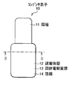
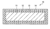
まず、図1および図2を参照して、本発明の一実施の形態に係る電解コンデンサの構成について簡単に説明する。図1および図2は電解コンデンサの主要部(コンデンサ素子10)の構成を表しており、図1は外観構成を示し、図2は図1に示したII−II線に沿った断面構成を拡大して示している。 First, with reference to FIG. 1 and FIG. 2, the structure of the electrolytic capacitor which concerns on one embodiment of this invention is demonstrated easily. 1 and 2 show the configuration of the main part (capacitor element 10) of the electrolytic capacitor, FIG. 1 shows the external configuration, and FIG. 2 is an enlarged cross-sectional configuration along the line II-II shown in FIG. As shown.
この電解コンデンサは、図1および図2に示したコンデンサ素子10に陽極リードおよび陰極リード(いずれも図示せず)が接続され、それらの陽極リードおよび陰極リードの双方が部分的に露出するようにコンデンサ素子10がモールド樹脂(図示せず)により周囲を覆われた構造を有するものである。コンデンサ素子10は、電解コンデンサの主要部として電気的反応を生じるものであり、例えば、図1および図2に示したように、陽極11と、この陽極11の周囲(一端部)を部分的に覆うように配設された誘電体層12と、この誘電体層12を覆うように配設された固体電解質層13と、この固体電解質層13を覆うように配設された陰極14とを含み、すなわち陽極11、誘電体層12、固体電解質層13および陰極14がこの順に積層された積層構造を有している。
In this electrolytic capacitor, an anode lead and a cathode lead (both not shown) are connected to the
陽極11は、拡面化(または粗面化)された表面凹凸構造を有する第1の電極層であり、例えば、アルミニウム(Al)、チタン(Ti)、タンタル(Ta)またはニオブ(Nb)などの弁作用金属を含んで構成されている。具体的には、陽極11は、例えば、アルミニウムまたはチタンなどの金属箔や、タンタルまたはニオブなどの金属焼結体である。なお、拡面化された陽極11の表面凹凸構造の詳細に関しては後述する(図3参照)。
The
誘電体層12は、例えば、弁作用金属により構成された陽極11の表層が陽極酸化されることにより形成された酸化皮膜である。この誘電体層12は、例えば、陽極11がアルミニウムより構成されている場合には、酸化アルミニウム(Al2 O3 )により構成されている。
The
固体電解質層13は、例えば、導電性高分子と、この導電性高分子の導電率を制御するためのドーパントとを含み、すなわち導電性高分子にドーパントが含有(ドープ)された構成を有している。導電性高分子は、例えば、ポリアニリン、ポリピロール、ポリチオフェン、ポリフランおよびこれらの誘導体を含む群のうちの少なくとも1種により構成されており、具体的な一例を挙げれば、ポリチオフェンの誘導体であるポリエチレンジオキシチオフェンなどにより構成されている。また、ドーパントは、例えば、アルキルベンゼンスルホン酸およびその塩、アルキルナフタレンスルホン酸およびその塩、ならびにリン酸を含む群のうちの少なくとも1種により構成されており、具体的な一例を挙げれば、パラトルエンスルホン酸鉄またはイソピロピルナフタレンスルホン酸鉄などにより構成されている。この固体電解質層13を含んでコンデンサ素子10が構成されている電解コンデンサは、いわゆる固体電解コンデンサである。
The
陰極14は、誘電体層12および固体電解質層13を挟んで陽極11に対向配置された第2の電極層である。この陰極14は、本来の電極としての機能の他に、所定の温度範囲内において温度の上昇に応じて抵抗が上昇し、より具体的には抵抗が指数関数的に上昇する機能(いわゆるPTC機能)を有しており、導電性粒子として金属粒子および導電性セラミック粒子のうちの少なくとも一方を含んで構成されている。このPTC機能を有する陰極14は、例えば、約60℃以上150℃以下の温度範囲内において抵抗が(常温の抵抗と比較して)約1000倍以上上昇するものである。
The
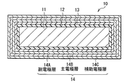
特に、陰極14は、例えば、2層以上の層が積層された積層構造を有しており、その2層以上の層のうちの少なくとも1つの層において、導電性粒子を含むと共にPTC機能を有している。具体的には、陰極14は、例えば、図2に示したように、導電性を確保するための主電極層14Bと、その主電極層14Bと固体電解質層13との間に配設され、主電極層14Bを固体電解質層13に電気的に接合させるための副電極層14Aと、主電極層14Bを挟んで副電極層14Aと反対側に配設され、導電性粒子を含むと共にPTC機能を有する補助電極層14Cとを含み、すなわち副電極層14A、主電極層14Bおよび補助電極層14Cがこの順に積層された3層構造を有している。この陰極14では、例えば、上記したように、副電極層14Aおよび主電極層14BがPTC機能を有しておらず、補助電極層14CのみがPTC機能を有している。
In particular, the
副電極層14Aは、例えば、カーボンを含んで構成されている。なお、副電極層14Aは、上記したように主電極層14Bを固体電解質層13に電気的に接合させる機能の他に、例えば、主電極層14Bを固体電解質層13に直接的に接触させた場合に、高温高湿環境中において主電極層14B中の特定成分(例えば銀(Ag))のマイグレーションを防止する機能も有している。
For example, the
主電極層14Bは、例えば、金属を含んで構成されており、具体的には銀(Ag)を含んで構成されている。
The
補助電極層14Cは、例えば、PTC機能を確保するための材料が下地(ここでは主電極層14B)の表面において膜化されることにより形成されたものであり、具体的にはPTC機能を確保するための材料(金属ペースト)として導電性粒子を含む液状高分子が膜化されることにより形成されたものである。「液状高分子」とは、室温(意図的に設定された高温環境を除き、一般的に電解コンデンサの製造工程が実施される通常環境の雰囲気温度であり、具体的には約15℃以上30℃以下の範囲内の雰囲気温度)において溶媒を利用せずに直接的、あるいは溶媒を利用して(溶媒に溶解されることにより)間接的に液体状態(流動状態)となり、塗布法、浸漬法または印刷法などの手法を使用して主電極層14Bの表面に供給されることにより直接的に膜化可能な特性を有する高分子である。上記した「液体状態(流動状態)」とは、主電極層14Bの表面に供給可能な限りにおいてペースト状態なども含む概念であり、例えば、約100cP以上1000000cP以下の範囲内の粘度を有する状態である。
The auxiliary electrode layer 14C is formed, for example, by forming a material for ensuring the PTC function on the surface of the base (here, the
この補助電極層14Cは、例えば、上記した液状高分子が膜化されることにより形成された主成分としての膜状高分子と、その膜状高分子中に保持された副成分としての導電性粒子とを含んで構成されている。すなわち、補助電極層14Cは、いわゆるポリマーPTC(P(Polymer )−PTC)層である。液状高分子は、例えば、不溶性熱可塑性高分子(室温において直接的に液体状態にならない上、室温において溶解可能な溶媒が存在しないために間接的にも液体状態にならない熱可塑性高分子)を除き、熱硬化性高分子および可溶性熱可塑性高分子(室温において直接的に液体状態にならないが、室温において溶解可能な溶媒が存在するために間接的に液体状態になる熱可塑性高分子)のうちの少なくとも1種を含むものである。この熱硬化性高分子としては、例えば、エポキシ樹脂などが挙げられ、一方、可溶性熱可塑性高分子としては、例えば、ポリフッ化ビニリデン(PVDF;Poly Vinylidene Fluoride)などが挙げられる。また、導電性粒子は、例えば、ニッケル(Ni)、銅(Cu)、アルミニウム(Al)、タングステン(W)、モリブデン(Mo)、亜鉛(Zn)、コバルト(Co)、白金(Pt)、金(Au)および銀(Ag)などの金属粒子、ならびに炭化タングステン(WC)、窒化チタン(TiN)、窒化ジルコニウム(ZrN)、炭化チタン(TiC)、ホウ化チタン(TiB2 )、ケイ化モリブデン(MoSi2 )およびホウ化タンタル(TaB2 )などの導電性セラミック粒子を含む群のうちの少なくとも1種である。 The auxiliary electrode layer 14C includes, for example, a film-like polymer as a main component formed by forming the above-described liquid polymer into a film, and a conductive material as a subcomponent held in the film-like polymer. It is comprised including particles. That is, the auxiliary electrode layer 14C is a so-called polymer PTC (P (Polymer) -PTC) layer. Liquid polymers include, for example, insoluble thermoplastic polymers (thermoplastic polymers that are not directly in a liquid state at room temperature and that are not indirectly in a liquid state because there is no solvent soluble at room temperature). , Thermosetting polymers and soluble thermoplastic polymers (thermoplastic polymers that are not directly in the liquid state at room temperature but are indirectly in the liquid state due to the presence of a soluble solvent at room temperature) It contains at least one kind. Examples of the thermosetting polymer include an epoxy resin, and examples of the soluble thermoplastic polymer include polyvinylidene fluoride (PVDF). The conductive particles include, for example, nickel (Ni), copper (Cu), aluminum (Al), tungsten (W), molybdenum (Mo), zinc (Zn), cobalt (Co), platinum (Pt), gold Metal particles such as (Au) and silver (Ag), as well as tungsten carbide (WC), titanium nitride (TiN), zirconium nitride (ZrN), titanium carbide (TiC), titanium boride (TiB 2 ), molybdenum silicide ( At least one of the group comprising conductive ceramic particles such as MoSi 2 ) and tantalum boride (TaB 2 ).
なお、参考までに、陽極リードおよび陰極リードは、例えば、いずれも鉄(Fe)または銅(Cu)などの金属や、これらの金属にめっき処理(例えば錫(Sn)めっきまたは錫鉛(SnPb)めっき)が施されためっき処理金属により構成されており、それぞれコンデンサ素子10のうちの陽極11および陰極14に接続されている。モールド樹脂は、例えば、エポキシ樹脂などの絶縁性樹脂により構成されている。
For reference, both the anode lead and the cathode lead are, for example, metals such as iron (Fe) or copper (Cu), and plating treatment (for example, tin (Sn) plating or tin lead (SnPb)) on these metals. It is made of a plated metal subjected to plating, and is connected to the
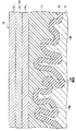
次に、図3を参照して、コンデンサ素子10の詳細な構成について説明する。図3は、図2に示したコンデンサ素子10の断面構成を部分的に拡大して表している。
Next, a detailed configuration of the
コンデンサ素子10では、例えば、図3に示したように、陽極11を覆うように誘電体層12、固体電解質層13および陰極14(副電極層14A,主電極層14B,補助電極層14C)がこの順に積層されている。このコンデンサ素子10では、陽極11の表面積を増大させることにより高容量化を実現するために、上記したように、その陽極11に拡面化処理(または粗面化処理)が施されており、すなわち陽極11が微細な表面凹凸構造を有している。この陽極11の表面凹凸構造を反映して、その陽極11を覆うように配設されている誘電体層12は微細な凹凸構造を有しており、この微細な凹凸構造を有する誘電体層12を覆うように固体電解質層13および陰極14(副電極層14A,主電極層14B,補助電極層14C)が配設されている。特に、誘電体層12は、凹凸構造のうちの凹部として複数の細孔12Hを構成しており、固体電解質層13は、誘電体層12により構成された複数の細孔12Hに部分的に入り込んでいる。
In the
図1〜図3に示した電解コンデンサでは、図示しない陽極リードおよび陰極リードを通じてコンデンサ素子10が通電されることにより、そのコンデンサ素子10において電荷が蓄えられる。この際、PTC機能を有する陰極14(補助電極層14C)を利用して、短絡時の発熱に起因する電解コンデンサの破壊が防止される。すなわち、例えば、電解コンデンサに過電圧や逆電圧が印加された場合に、誘電体層12が部分的に破損して短絡したことに起因して陽極11と固体電解質層13および陰極14(副電極層14A,主電極層14B,補助電極層14C)との間に過電流が流れて発熱すると、その短絡時の発熱に基づいて補助電極層14Cの温度が上昇することにより抵抗が指数関数的に上昇する結果、コンデンサ素子10中を流れる過電流が抑制されるため、その過電流に起因してコンデンサ素子10が破壊されにくくなる。なお、補助電極層14Cの温度が上昇する要因としては、例えば、上記した短絡時の発熱の他に、過電流に起因するジュール熱も含まれる。こののち、補助電極層14Cの温度が低下すると、その温度低下に応じて補助電極層14Cの抵抗が低下するため、コンデンサ素子10が通電可能な状態に復帰する。
In the electrolytic capacitor shown in FIGS. 1 to 3, electric charge is stored in the
なお、補助電極層14CがPTC機能を有する原理は、以下の通りである。すなわち、温度上昇前の段階では、補助電極層14Cを構成している膜状高分子中において導電性粒子がチェーン(いわゆる導電パス)を構築しており、そのチェーンが膜状高分子により安定に保持されているため、そのチェーンの存在に基づいて補助電極層14Cが低抵抗状態にある。しかしながら、補助電極層14Cの温度が上昇すると、膜状高分子の膨張現象に起因してチェーンが切断されるため、補助電極層14Cが高抵抗状態になる。もちろん、補助電極層14Cの温度が低下すると、膜状高分子の収縮現象に基づいてチェーンが再構築されるため、補助電極層14Cが再び低抵抗状態となる。したがって、上記したチェーンの構築・切断・再構築メカニズムを利用して補助電極層14Cの抵抗状態が可逆的に変化可能なため、その補助電極層14CがPTC機能を有するのである。 The principle that the auxiliary electrode layer 14C has the PTC function is as follows. That is, before the temperature rises, the conductive particles construct a chain (so-called conductive path) in the film-like polymer constituting the auxiliary electrode layer 14C, and the chain is more stable by the film-like polymer. Since it is held, the auxiliary electrode layer 14C is in a low resistance state based on the presence of the chain. However, when the temperature of the auxiliary electrode layer 14C rises, the chain is cut due to the expansion phenomenon of the film-like polymer, so that the auxiliary electrode layer 14C enters a high resistance state. Of course, when the temperature of the auxiliary electrode layer 14C is lowered, the chain is reconstructed based on the contraction phenomenon of the film-like polymer, so that the auxiliary electrode layer 14C is again in the low resistance state. Therefore, since the resistance state of the auxiliary electrode layer 14C can be reversibly changed using the above-described chain construction / cutting / reconstruction mechanism, the auxiliary electrode layer 14C has a PTC function.
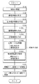
次に、図1〜図4を参照して、本発明の一実施の形態に係る電解コンデンサの製造方法として、図1〜図3に示したコンデンサ素子10を備えた電解コンデンサの製造方法について説明する。図4は、電解コンデンサの製造方法に関する製造工程の流れを説明するためのものである。なお、以下では、電解コンデンサ(コンデンサ素子10)を構成する各構成要素の材質に関しては既に詳細に説明したので、その説明を随時省略するものとする。
Next, with reference to FIGS. 1-4, the manufacturing method of the electrolytic capacitor provided with the capacitor |
電解コンデンサを製造する際には、まず、図1〜図3に示したコンデンサ素子10を形成する。すなわち、まず、陽極11として、例えば、拡面化処理が施された処理済みの弁作用金属箔(例えばアルミニウム箔やチタン箔)、すなわち微細な表面凹凸構造を有する陽極11を準備する(図4;ステップS101)。この陽極11としては、例えば、上記した拡面化処理済みの弁作用金属箔に代えて、タンタルまたはニオブなどの弁作用金属焼結体も使用可能である。なお、陽極11を準備する際には、例えば、上記したように拡面化処理済みの弁作用金属箔を使用する代わりに、未処理の弁作用金属箔を使用し、化学的または電気化学的エッチングを使用して弁作用金属箔に拡面化処理を施すことにより陽極11を形成してもよい。
When manufacturing an electrolytic capacitor, first, the
続いて、陽極11の表層を陽極酸化することにより、その陽極11の周囲を部分的に覆うように酸化皮膜よりなる誘電体層12を形成する(図4;ステップS102)。この誘電体層12としては、例えば、陽極11の形成材料としてアルミニウム箔を使用した場合には、酸化アルミニウムの皮膜により構成されるように誘電体層12を形成可能である。この誘電体層12を形成する際には、例えば、陽極11を化成溶液に浸漬させたのち、その陽極12に電圧を印加することにより陽極酸化反応を進行させるようにする。この化成溶液としては、例えば、ホウ酸アンモニウム、リン酸アンモニウムまたは有機酸アンモニウムなどを含む緩衝溶液を使用し、具体的にはアジピン酸アンモニウム水溶液などを使用する。なお、陽極11に印加する電圧は、例えば、誘電体層12の形成厚さに応じて数V〜数百Vの範囲内で自由に設定可能である。
Subsequently, the surface layer of the
続いて、誘電体層12を覆うように、ドーパントがドープされた導電性高分子を生成することにより、その導電性高分子を含むように固体電解質層13を形成する(図4;ステップS103)。この固体電解質層13を形成する際には、例えば、単量体、ドーパントおよび酸化剤を溶媒に分散させた溶液(単量体溶液)を調製し、その単量体溶液を誘電体層12の表面に塗布したのち、単量体溶液を加熱し、その単量体溶液中の酸化剤を使用して単量体を酸化重合させることにより導電性高分子を生成する。なお、導電性高分子を生成したのちには、例えば、水、アルコール、アセトンまたはヘキサンなどを使用して導電性高分子を洗浄することにより、導電性高分子に含まれている未重合の単量体、導電性高分子にドープされなかった過剰なドーパント、ならびに使用済みの酸化剤などを洗い流して除去するのが好ましい。単量体溶液の加熱温度および加熱時間は、例えば、単量体の反応性(重合性)や酸化剤の反応性(酸化力)等を考慮して適宜設定可能である。
Subsequently, a conductive polymer doped with a dopant is generated so as to cover the
なお、単量体溶液を調整する際には、単量体として、例えば、アニリン、ピロール、チオフェン、フラン、チオフェンビニレン、イソチアナフテン、アセチレン、p−フェニレン、フェニレンビニレン、メトキシビニレン、メトキシフェニレン、フェニレンスルファイド、フェニレンオキシド、アントラセン、ナフタレン、ピレン、アズレン、セレノフェン、テルロフェンおよびこれらの誘導体を含む群のうちの少なくとも1種を使用し、具体的には3,4−エチレンジオキシチオフェンなどを使用する。 In preparing the monomer solution, examples of the monomer include aniline, pyrrole, thiophene, furan, thiophene vinylene, isothianaphthene, acetylene, p-phenylene, phenylene vinylene, methoxy vinylene, methoxy phenylene, Use at least one of the group comprising phenylene sulfide, phenylene oxide, anthracene, naphthalene, pyrene, azulene, selenophene, tellurophene and their derivatives, specifically 3,4-ethylenedioxythiophene, etc. To do.
また、ドーパントとして、例えば、ドナー型またはアクセプター型のいずれのドーパントも使用可能であり、下記の一連の材料を含む群のうちの少なくとも1種を使用する。ドナー型のドーパントとしては、例えば、リチウム(Li)、ナトリウム(Na)またはカリウム(K)などのアルカリ金属や、カルシウム(Ca)などのアルカリ土類金属等が挙げられる。一方、アクセプター型のドーパントとしては、例えば、塩素(Cl2 )、臭素(Br2 )またはヨウ素(I2 )などのハロゲンや、フッ化リン(PF3 )、フッ化ヒ素(AsF5 )またはフッ化ホウ素(BF3 )などのルイス酸や、フッ化水素(HF)、塩化水素(HCl)、硝酸(HNO3 )、硫酸(H2 SO4 )、リン酸(H3 PO4 )または過塩素酸(HClO4 )などのプロトン酸や、アルキルベンゼンスルホン酸(例えばパラトルエンスルホン酸)、アルキルナフタレンスルホン酸またはこれらの塩(例えばパラトルエンスルホン酸ナトリウムまたはアルキルナフタレンスルホン酸ナトリウム)や、塩化鉄(FeCl3 )、過塩素酸鉄(FeOCl2 )、塩化チタン(TiCl4 )または塩化タングステン(WCl3 )などの遷移金属化合物や、塩素イオン(Cl- )、臭素イオン(Br- )、ヨウ素イオン(I- )、過塩素酸イオン(ClO4 -)、フッ化リンイオン(PF3 -)、フッ化ホウ素イオン(BF3 -)またはフッ化ヒ素イオン(AsF3 -)などの電解質アニオン等が挙げられる。 In addition, as the dopant, for example, either a donor-type or acceptor-type dopant can be used, and at least one of a group including the following series of materials is used. Examples of the donor-type dopant include alkali metals such as lithium (Li), sodium (Na), and potassium (K), and alkaline earth metals such as calcium (Ca). On the other hand, examples of acceptor-type dopants include halogens such as chlorine (Cl 2 ), bromine (Br 2 ), and iodine (I 2 ), phosphorus fluoride (PF 3 ), arsenic fluoride (AsF 5 ), and fluorine. Lewis acids such as boron fluoride (BF 3 ), hydrogen fluoride (HF), hydrogen chloride (HCl), nitric acid (HNO 3 ), sulfuric acid (H 2 SO 4 ), phosphoric acid (H 3 PO 4 ) or perchlorine Protic acids such as acids (HClO 4 ), alkylbenzene sulfonic acids (eg, paratoluene sulfonic acid), alkyl naphthalene sulfonic acids or salts thereof (eg, sodium paratoluene sulfonate or sodium alkyl naphthalene sulfonate), iron chloride (FeCl 3), perchlorate (FeOCl 2), a transition such as titanium chloride (TiCl 4) or tungsten chloride (WCl 3) Or group compound, chlorine ion (Cl -), a bromine ion (Br -), iodide ion (I -), perchlorate ion (ClO 4 -), fluoride phosphorus (PF 3 -), boron fluoride ions (BF 3 − ) or electrolyte anions such as arsenic fluoride ion (AsF 3 − ).
さらに、酸化剤として、例えば、ヨウ素または臭素などのハロゲンや、五フッ化ケイ素(SiF5 )などの金属ハロゲン化物や、硫酸などのプロトン酸や、三酸化硫黄(SO3 )などの酸素化合物や、硫酸セリウム(Ce(SO4 )2 )などの硫酸塩や、過硫酸ナトリウム(Na2 S2 O8 )などの過硫酸塩や、過酸化水素(H2 O2 )などの過酸化物や、アルキルベンゼンスルホン酸塩(例えばパラトルエンスルホン酸鉄)などを使用する。 Further, as the oxidizing agent, for example, halogen such as iodine or bromine, metal halide such as silicon pentafluoride (SiF 5 ), protonic acid such as sulfuric acid, oxygen compound such as sulfur trioxide (SO 3 ), , Sulfates such as cerium sulfate (Ce (SO 4 ) 2 ), persulfates such as sodium persulfate (Na 2 S 2 O 8 ), peroxides such as hydrogen peroxide (H 2 O 2 ) Alkylbenzene sulfonate (for example, iron iron p-toluenesulfonate) is used.
なお、溶媒として、例えば、水や、ブタノールなどの有機溶媒等を使用する。 As the solvent, for example, water or an organic solvent such as butanol is used.
上記した酸化重合反応を経て生成される導電性高分子は、例えば、ポリアニリン、ポリピロール、ポリチオフェン、ポリフラン、ポリチオフェンビニレン、ポリイソチアナフテン、ポリアセチレン、ポリ−p−フェニレン、ポリフェニレンビニレン、ポリメトキシビニレン、ポリメトキシフェニレン、ポリフェニレンスルファイド、ポリフェニレンオキシド、ポリアントラセン、ポリナフタレン、ポリピレン、ポリアズレン、ポリセレノフェン、ポリテルロフェンおよびこれらの誘導体を含む群のうちの少なくとも1種であり、具体的にはポリエチレンジオキシチオフェンである。この導電性高分子としては、例えば、高分子骨格中に一次元的連鎖を有し、かつ電子供与性機能または電子受容性機能(いわゆるドーパミン機能)を有する共役系高分子が好ましい。 The conductive polymer produced through the above oxidative polymerization reaction is, for example, polyaniline, polypyrrole, polythiophene, polyfuran, polythiophene vinylene, polyisothianaphthene, polyacetylene, poly-p-phenylene, polyphenylene vinylene, polymethoxy vinylene, poly At least one member selected from the group comprising methoxyphenylene, polyphenylene sulfide, polyphenylene oxide, polyanthracene, polynaphthalene, polypyrene, polyazulene, polyselenophene, polytellurophene and their derivatives, specifically polyethylenedioxy Thiophene. As the conductive polymer, for example, a conjugated polymer having a one-dimensional chain in the polymer skeleton and having an electron donating function or an electron accepting function (so-called dopamine function) is preferable.
引き続き、電解コンデンサの製造工程について説明する。陽極11、誘電体層12および固体電解質層13がこの順に積層された積層構造を形成したのち、その固体電解質層13を覆うように、PTC機能を有する陰極14を形成する(図4;ステップS104)。
Next, the manufacturing process of the electrolytic capacitor will be described. After forming a laminated structure in which the
この陰極14の形成手順は、例えば、以下の通りである。すなわち、まず、固体電解質層13の表面にカーボンペーストを塗布したのち、そのカーボンペーストを乾燥して膜化することにより、副電極層14Aを形成する(ステップS1041)。続いて、副電極層14Aの表面に金属ペーストを塗布したのち、その金属ペーストを乾燥して膜化することにより、主電極層14Bを形成する(ステップS1042)。この主電極層14Bを形成する際には、例えば、金属ペーストとして銀(Ag)ペーストを使用する。続いて、PTC機能を確保するための材料として、液状高分子および導電性粒子を含む金属ペーストを準備する(ステップS1043)。この金属ペーストを準備する際には、例えば、液状高分子としてエポキシ樹脂などの熱硬化性高分子やポリフッ化ビニリデン(PVDF)などの可溶性熱可塑性高分子のうちの少なくとも1種を使用すると共に、導電性粒子として金属粒子および導電性セラミック粒子のうちの少なくとも一方を使用し、具体的にはニッケル(Ni)、銅(Cu)、アルミニウム(Al)、タングステン(W)、モリブデン(Mo)、亜鉛(Zn)、コバルト(Co)、白金(Pt)、金(Au)および銀(Ag)などの金属粒子、ならびに炭化タングステン(WC)、窒化チタン(TiN)、窒化ジルコニウム(ZrN)、炭化チタン(TiC)、ホウ化チタン(TiB2 )、ケイ化モリブデン(MoSi2 )およびホウ化タンタル(TaB2 )などの導電性セラミック粒子を含む群のうちの少なくとも1種を使用する。特に、導電性粒子として金属粒子を使用する場合には、例えば、フィラメント状の金属粒子を使用するのが好ましい。最後に、主電極層14Bの表面に金属ペーストを供給したのち、その金属ペーストを乾燥して膜化することにより、液状高分子が膜化した膜状高分子と、その膜状高分子中に保持された導電性粒子とを含むように、PTC機能を有する補助電極層14Cを形成する(ステップS1044)。この金属ペーストの供給方法としては、例えば、塗布法(例えばスプレー法、ローラ法またはスピンコート法)、浸漬法(いわゆるディップ法)、あるいは印刷法(例えばスクリーン印刷またはタンポ印刷)などを使用可能である。これにより、副電極層14A、主電極層14Bおよび補助電極層14Cを含む3層構造を有するように陰極14が形成される。この結果、陽極11、誘電体層12、固体電解質層13および陰極14(副電極層14A,主電極層14B,補助電極層14C)がこの順に積層された積層構造を有するコンデンサ素子10が完成する。
The formation procedure of the
コンデンサ素子10を形成したのち、このコンデンサ素子10を使用して電解コンデンサを組み立てる。すなわち、例えば、コンデンサ素子10のうちの陽極11に陽極リードを接続させると共に、陰極14に陰極リードを接続させたのち(図4;ステップS105)、陽極リードおよび陰極リードの双方が部分的に露出するようにコンデンサ素子10の周囲をモールド樹脂で被覆する(図4;ステップS106)。これにより、コンデンサ素子10に陽極リードおよび陰極リードが接続され、それらの陽極リードおよび陰極リードの双方が部分的に露出するようにコンデンサ素子10がモールド樹脂により周囲を覆われた構造を有する電解コンデンサが完成する。なお、コンデンサ素子10に陽極リードおよび陰極リードを接続させる際には、例えば、溶接処理またはかしめ加工を使用して直接的に接続させるようにしてもよいし、あるいは導電性接着剤を使用して間接的に接続させるようにしてもよい。
After the
本実施の形態に係る電解コンデンサの製造方法では、PTC機能を有するように陰極14、具体的には補助電極層14Cを形成したので、上記したPTC機能の原理に基づき、陰極14のうちの補助電極層14CにPTC機能が付与される。この場合には、導電性粒子として金属粒子および導電性セラミック粒子のうちの少なくとも一方を含むように補助電極層14Cを形成したことにより、それらの金属粒子または導電性セラミック粒子の低抵抗特性に基づいて電解コンデンサの抵抗特性が低下する。これにより、PTC機能を利用して短絡時の発熱に起因する電解コンデンサの破壊を防止しつつ、その電解コンデンサの抵抗特性を低下させることが可能となる。したがって、PTC機能を有する電解コンデンサの抵抗特性を可能な限り低下させることができる。
In the method of manufacturing an electrolytic capacitor according to the present embodiment, the
特に、本実施の形態では、PTC機能を有する補助電極層14Cを形成する際に、主電極層14Bの表面に金属ペースト(液状高分子,導電性粒子)を供給して膜化することにより補助電極層14C(膜状高分子,導電性粒子)を形成したので、例えば、あらかじめ補助電極層14Cをシート状(導電性高分子シート)に成形し、そのシート状の補助電極層14Cを主電極層14Bの表面に接合(例えば接着または熱圧着)させる場合と比較して、その接合箇所に基づく接触抵抗が含まれない分だけ電解コンデンサの抵抗特性が低下する。したがって、この観点においても電解コンデンサの低抵抗化に寄与することができる。
In particular, in the present embodiment, when forming the auxiliary electrode layer 14C having the PTC function, the metal electrode (liquid polymer, conductive particles) is supplied onto the surface of the
また、上記した他、本実施の形態に係る電解コンデンサでは、PTC機能が陰極14(補助電極層14C)において確保されつつ抵抗特性が低下するため、可能な限り低抵抗でPTC機能を確保することができる。 In addition to the above, in the electrolytic capacitor according to the present embodiment, the PTC function is ensured at the cathode 14 (auxiliary electrode layer 14C) while the resistance characteristics deteriorate, so the PTC function is ensured with as low resistance as possible. Can do.
なお、本実施の形態では、PTC機能を有する補助電極層14Cを形成する際に、PTC機能を確保するための材料(液状高分子,導電性粒子)を主電極層14Bの表面に供給して膜化することにより補助電極層14Cを形成するようにしたが、必ずしもこれに限られるものではなく、例えば、図5に示したように、主電極層14Bの表面において補助電極層14Cを膜化形成する手法に代えて、別途形成した補助電極層14Cを主電極層14Bの表面に接続させるようにしてもよい。図5は電解コンデンサの製造方法に関する変形例を説明するためのものであり、図4に対応する製造工程の流れを示している。この電解コンデンサの製造方法では、図1〜図3および図5に示したように、陽極11を準備し(ステップS201)、その陽極11上に誘電体層12および固体電解質層13を形成したのち(ステップS202,S203)、その固体電解質層13上に、副電極層14Aおよび主電極層14Bと共に別途形成した補助電極層14Cを含むように陰極14を形成する(ステップS204)。具体的には、固体電解質層13上に副電極層14Aを形成し(ステップS2041)、引き続き副電極層14A上に主電極層14Bを形成したのち(ステップS2042)、PTC機能を確保するための材料(液状高分子,導電性粒子)をシート状に成形することにより導電性高分子シートを形成し(ステップS2043)、その導電性高分子シートを補助電極層14Cとして主電極層14Bの表面に接合させることにより(ステップS2044)、副電極層14A、主電極層14Bおよび補助電極層14Cを含む3層構造を有するように陰極14を形成する。この導電性高分子シートを主電極層14Cに接合させる処理としては、例えば、接着処理や熱圧着処理を使用可能である。なお、導電性高分子シートを使用して補助電極層14Cを形成する際には、例えば、その導電性高分子シートの形成材料として、熱硬化性高分子や可溶性熱可塑性高分子などの液状高分子に限らず、ポリエチレン(PE;Polyethylene)などの不溶性熱可塑性高分子も使用可能である。これにより、陽極11、誘電体層12、固体電解質層13および陰極14(副電極層14A,主電極層14B,補助電極層14C)がこの順に積層された積層構造を有するコンデンサ素子10が形成される。こののち、コンデンサ素子10のうちの陽極11および陰極14に陽極リードおよび陰極リードをそれぞれ接続させると共に(ステップS205)、陽極リードおよび陰極リードの双方が部分的に露出するようにコンデンサ素子10の周囲をモールド樹脂で被覆することにより(ステップS206)、電解コンデンサが完成する。この場合においても、陰極14のうちの補助電極層14CにPTC機能が付与されるため、上記実施の形態と同様の効果を得ることができる。ただし、上記したように、補助電極層14Cを主電極層14Bに接合させた場合には、主電極層14Bの表面において補助電極層14Cを膜化形成した場合と比較して、主電極層14Bと補助電極層14Cとの間の接触抵抗分だけ電解コンデンサの抵抗特性が上昇し得るため、留意する必要がある。なお、図5に示した電解コンデンサの製造方法に関する上記した以外の手順は、例えば、図4に示した場合と同様である。
In this embodiment, when forming the auxiliary electrode layer 14C having the PTC function, a material (liquid polymer, conductive particles) for ensuring the PTC function is supplied to the surface of the
また、本実施の形態では、陰極14(補助電極層14A,主電極層14B,補助電極層14C)のうちの補助電極層14CのみがPTC機能を有するようにしたが、必ずしもこれに限られるものではなく、例えば、補助電極層14Cに代えて副電極層14AのみがPTC機能を有するようにしてもよいし、主電極層14AのみがPTC機能を有するようにしてもよいし、副電極層14A、主電極層14Bおよび補助電極層14Cのうちの任意の2つの組み合わせのみがPTC機能を有するようにしてもよいし、あるいは副電極層14A、主電極層14Bおよび補助電極層14Cの全てがPTC機能を有するようにしてもよい。副電極層14AのみがPTC機能を有するようにする場合には、例えば、副電極層14Aの形成材料(PTC機能を確保するための材料)として導電性粒子を含むカーボンペーストを使用し、上記実施の形態において補助電極層14Cを形成した場合と同様の工程を経て副電極層14Aを形成することにより、その副電極層14AにPTC機能を付与することが可能である。この場合には、例えば、導電性粒子として上記実施の形態において説明した金属粒子および導電性粒子のうちの少なくとも一方を使用すると共に、主電極層14Bおよび補助電極層14Cの形成材料(PTC機能を確保し得ない材料)として一般的な金属ペースト(例えば銀ペースト等)を使用する。また、主電極層14BのみがPTC機能を有するようにする場合には、例えば、上記実施の形態において補助電極層14Cを形成した場合と同様の工程を経て主電極層14Bを形成することにより、その主電極層14BにPTC機能を付与することが可能である。この場合には、例えば、補助電極層14Cの形成材料(PTC機能を確保し得ない材料)として一般的な金属ペースト(例えば銀ペースト等)を使用する。なお、副電極層14A、主電極層14Bおよび補助電極層14Cの全てがPTC機能を有するようにする場合には、例えば、上記したPTC機能を有する副電極層14A、PTC機能を有する主電極層14B、ならびにPTC機能を有する補助電極層14Cを組み合わせればよい。これらの場合においても、陰極14にPTC機能が付与されるため、上記実施の形態と同様の効果を得ることができる。
In the present embodiment, only the auxiliary electrode layer 14C of the cathode 14 (
また、本実施の形態では、陰極14が3層構造(副電極層14A,主電極層14B,補助電極層14C)を有するようにしたが、必ずしもこれに限られるものではなく、その陰極14の積層構造数は2層以上の範囲で自由に変更可能である。この場合においても、陰極14が電極として機能し得るだけの抵抗特性を有すると共にPTC機能を確保し得る限り、上記実施の形態と同様の効果を得ることができる。もちろん、この場合においても、例えば、陰極14の積層構造中の一部の層のみがPTC機能を有するようにしてもよいし、あるいは積層構造中の全ての層がPTC機能を有するようにしてもよい。
In the present embodiment, the
また、本実施の形態では、PTC機能を有する陰極14が積層構造(副電極層14A,主電極層14B,補助電極層14C)を有するようにしたが、必ずしもこれに限られるものではなく、例えば、図6に示したように、陰極14が単層構造を有するようにしてもよい。この場合には、上記実施の形態において説明したPTC機能を有する補助電極層14Cに相当する構成となるように、陰極14を構成する。この場合においても、上記実施の形態と同様の効果を得ることができる。なお、図6に示したコンデンサ素子10に関する上記以外の構成的特徴は、例えば、図2に示した場合と同様である。
In the present embodiment, the
次に、本発明の具体的な実施例について説明する。 Next, specific examples of the present invention will be described.
上記実施の形態において説明した電解コンデンサの製造方法を使用して、電解コンデンサを製造した。すなわち、まず、陽極として処理済み(拡面化処理済み)のアルミニウム箔を準備したのち、化成溶液中においてアルミニウム箔に電圧(=23V)を印加し、陽極酸化反応を進行させて酸化アルミニウム皮膜を形成することにより、誘電体層を形成した。この誘電体層の形成後、アジピン酸アンモニウム水溶液中で容量を測定したところ、理論容量は約100μFであった。続いて、単量体、ドーパントおよび酸化剤を溶媒に分散させた単量体溶液を準備し、誘電体層を形成済みの陽極を単量体溶液に30秒間に渡って浸漬させることにより、その誘電体層の表面に単量体溶液を付着させたのち、陽極を0.5mm/秒で引き上げて室温乾燥させた。続いて、単量体溶液に浸漬済みの陽極を乾燥器に投入して加熱し、その単量体溶液に含まれている酸化剤を使用して単量体を酸化重合させることにより、ドーパントがドープされた導電性高分子を含むように固体電解質層を形成した。続いて、固体電解質層の表面にカーボンペーストを塗布して乾燥させることにより副電極層を形成し、引き続き副電極層の表面に銀ペーストを塗布して乾燥させることにより主電極層を形成したのち、その主電極層層を覆うようにPTC機能を有する補助電極層を形成することにより、これらの副電極層、主電極層および補助電極層を含む3層構造を有するようにPTC機能を有する陰極を形成した。これにより、陽極、誘電体層、固体電解質層および陰極(副電極層,主電極層,補助電極層)がこの順に積層された積層構造を有するコンデンサ素子が形成された。最後に、導電性接着剤(銀接着剤)を使用してコンデンサ素子に銅製の陽極リードおよび陰極リードを接続させたのち、モールド樹脂としてエポキシ樹脂で陽極リードおよび陰極リードが部分的に露出するようにコンデンサ素子の周囲を覆うことにより、電解コンデンサが完成した。 An electrolytic capacitor was manufactured using the electrolytic capacitor manufacturing method described in the above embodiment. That is, first, a treated (surface-enhanced) aluminum foil is prepared as an anode, and then a voltage (= 23 V) is applied to the aluminum foil in the chemical conversion solution to advance the anodic oxidation reaction to form an aluminum oxide film. By forming, a dielectric layer was formed. After the formation of this dielectric layer, the capacity was measured in an aqueous solution of ammonium adipate. The theoretical capacity was about 100 μF. Subsequently, a monomer solution in which a monomer, a dopant and an oxidant are dispersed in a solvent is prepared, and the anode on which the dielectric layer has been formed is immersed in the monomer solution for 30 seconds. After the monomer solution was attached to the surface of the dielectric layer, the anode was pulled up at 0.5 mm / second and dried at room temperature. Subsequently, the anode immersed in the monomer solution is put into a dryer and heated, and the dopant is oxidized by oxidative polymerization of the monomer using the oxidizing agent contained in the monomer solution. A solid electrolyte layer was formed to include the doped conductive polymer. Subsequently, a carbon paste is applied to the surface of the solid electrolyte layer and dried to form a sub-electrode layer. Subsequently, a silver paste is applied to the surface of the sub-electrode layer and dried to form the main electrode layer. A cathode having a PTC function so as to have a three-layer structure including the sub-electrode layer, the main electrode layer and the auxiliary electrode layer by forming an auxiliary electrode layer having a PTC function so as to cover the main electrode layer Formed. As a result, a capacitor element having a laminated structure in which the anode, the dielectric layer, the solid electrolyte layer, and the cathode (sub-electrode layer, main electrode layer, auxiliary electrode layer) were laminated in this order was formed. Finally, after connecting the copper anode lead and cathode lead to the capacitor element using a conductive adhesive (silver adhesive), the anode lead and cathode lead are partially exposed with epoxy resin as the mold resin. The electrolytic capacitor was completed by covering the periphery of the capacitor element.
なお、固体電解質層の形成手順は、以下の通りである。すなわち、まず、単量体として3,4−エチレンジオキシチオフェン(バイエル株式会社製Baytron M (商品名))、ならびにドーパント兼酸化剤としてパラトルエンスルホン酸鉄(III)50%ブタノール溶液(バイエル株式会社製Baytron C (商品名))を氷水で十分に冷却したのち、これらの単量体およびドーパント兼酸化剤をそれぞれ0.867g,10.4g秤量し、氷水で冷却しながらマグネチックスターラーで混合・攪拌することにより単量体溶液を調製した。続いて、誘電体層を形成済みの陽極を上記した浸漬条件で単量体溶液に浸漬させることにより、その誘電体層の表面に単量体溶液を付着させた。続いて、単量体溶液が付着された誘電体層を室温下において1時間程度放置したのち、その単量体溶液を加熱して単量体を酸化重合させることにより、誘電体層を覆うように導電性高分子としてポリエチレンジオキシチオフェンを生成した。この際、加熱条件は加熱温度=100℃、加熱時間=15分間とした。最後に、蒸留水を使用して導電性高分子を十分に洗浄することにより、未重合の単量体、過剰なドーパント、ならびに使用済みの酸化剤などを洗い流したのち、その導電性高分子を乾燥させた。なお、導電性高分子を形成する際には、上記した導電性高分子の生成手順を3回繰り返し、特に、酸化重合反応の完了時ごとに蒸留水やエタノールを使用して導電性高分子を洗浄することにより、未重合の単量体、余剰なドーパントならびに使用済みの酸化剤を随時除去した。これにより、導電性高分子を含む固体電解質層が形成された。 The procedure for forming the solid electrolyte layer is as follows. First, 3,4-ethylenedioxythiophene as a monomer (Baytron M (trade name) manufactured by Bayer Co., Ltd.) and 50% butanol solution of iron (III) paratoluenesulfonate as a dopant and oxidizing agent (Bayer shares) After sufficiently cooling the company's Baytron C (trade name) with ice water, weigh out 0.867 g and 10.4 g of these monomers and dopant / oxidizer, and mix them with a magnetic stirrer while cooling with ice water. -A monomer solution was prepared by stirring. Subsequently, the monomer solution was attached to the surface of the dielectric layer by immersing the anode on which the dielectric layer had been formed in the monomer solution under the immersion conditions described above. Subsequently, the dielectric layer to which the monomer solution is attached is allowed to stand at room temperature for about 1 hour, and then the monomer solution is heated to oxidatively polymerize the monomer so as to cover the dielectric layer. Polyethylenedioxythiophene was produced as a conductive polymer. At this time, the heating conditions were heating temperature = 100 ° C. and heating time = 15 minutes. Finally, the conductive polymer is thoroughly washed with distilled water to wash away unpolymerized monomers, excess dopant, used oxidant, etc., and then remove the conductive polymer. Dried. When forming the conductive polymer, the above-mentioned procedure for generating the conductive polymer is repeated three times. In particular, the conductive polymer is prepared using distilled water or ethanol every time the oxidative polymerization reaction is completed. By washing, unpolymerized monomer, excess dopant and used oxidizing agent were removed as needed. Thereby, a solid electrolyte layer containing a conductive polymer was formed.
上記した電解コンデンサの製造方法を使用して、PTC機能を有する陰極(補助電極層)の構成を以下のように変化させながら本発明の電解コンデンサ(実施例1〜7)を製造したのち、各電解コンデンサの諸特性を調べた。なお、本発明の電解コンデンサの諸特性を調べる際には、その性能を比較評価するために、陰極の構成を以下のように変化させながら比較例の電解コンデンサ(比較例1〜4)を製造し、各電解コンデンサの諸特性も併せて調べた。 After manufacturing the electrolytic capacitor (Examples 1 to 7) of the present invention while changing the configuration of the cathode (auxiliary electrode layer) having the PTC function as follows using the above-described electrolytic capacitor manufacturing method, Various characteristics of electrolytic capacitors were investigated. When investigating the characteristics of the electrolytic capacitor of the present invention, comparative electrolytic capacitors (Comparative Examples 1 to 4) were manufactured while changing the configuration of the cathode as follows in order to compare and evaluate the performance. The characteristics of each electrolytic capacitor were also investigated.
(実施例1)
補助電極層の形成材料(金属ペースト)として、液状高分子(膜状高分子)として熱硬化性高分子、具体的には大日本インキ化学工業株式会社製のエポキシ樹脂 EPICLON850(エポキシ当量=190g/eq)と旭電化工業株式会社製のエポキシ樹脂 EP4005(エポキシ当量=510g/eq)との混合物(エポキシ樹脂α;配合重量比(EPICLON850:EP4005)=75:25)を使用すると共に、導電性粒子として金属粒子、具体的にはINCO Limited社製のフィラメント状ニッケルパウダ(Ni) Type255(平均粒径=2.2μm〜2.8μm,見かけ密度=0.50g/cm3 〜0.65g/cm3 ,比表面積=0.68m2 /g,添加重量比(液状高分子:導電性粒子)=40:60)を使用し、主電極層の表面に金属ペーストを塗布したのちに窒素雰囲気下において130℃で加熱硬化させることにより、0.3mmの厚さとなるように補助電極層を形成した。なお、金属ペーストとしては、上記した液状高分子および導電性粒子と共に、硬化補助剤として、大日本インキ化学工業株式会社製の硬化剤 B570(酸無水物当量=168g/eq,液状高分子に対して当量比=1:1)と、味の素ファインテクノ株式会社製の硬化促進剤 PN−40J(添加量=液状高分子の重量に対して1重量%)とを含むものを使用した。
(Example 1)
As a material for forming the auxiliary electrode layer (metal paste), a thermosetting polymer as a liquid polymer (film-like polymer), specifically, an epoxy resin EPICLON850 manufactured by Dainippon Ink and Chemicals, Inc. (epoxy equivalent = 190 g / eq) and epoxy resin EP4005 (epoxy equivalent = 510 g / eq) manufactured by Asahi Denka Kogyo Co., Ltd. (epoxy resin α; blended weight ratio (EPICLON850: EP4005) = 75: 25) and conductive particles As metal particles, specifically, filamentary nickel powder (Ni) Type 255 manufactured by INCO Limited (average particle size = 2.2 μm to 2.8 μm, apparent density = 0.50 g / cm 3 to 0.65 g / cm 3 specific surface area = 0.68 m 2 / g, the addition weight ratio (liquid polymer: conductive particles) = 40: 60) using a main electrode By heat curing at 130 ° C. under a nitrogen atmosphere was coated a metal paste on the surface of, and forming an auxiliary electrode layer to have a thickness of 0.3 mm. In addition, as a metal paste, the curing agent B570 (acid anhydride equivalent = 168 g / eq, manufactured by Dainippon Ink & Chemicals, Inc.) as a curing auxiliary agent together with the above-described liquid polymer and conductive particles. Equivalent ratio = 1: 1) and a curing accelerator PN-40J manufactured by Ajinomoto Fine Techno Co., Ltd. (addition amount = 1 wt% based on the weight of the liquid polymer) was used.
(実施例2)
液状高分子(膜状高分子)としてエポキシ樹脂αに代えて日本化薬株式会社製のエポキシ樹脂(エポキシ樹脂β) AK−601(エポキシ当量=153g/eq)を使用した点を除き、実施例1と同様の手順を経ることにより補助電極層を形成した。
(Example 2)
Example, except that Epoxy Resin (Epoxy Resin β) AK-601 (Epoxy Equivalent = 153 g / eq) manufactured by Nippon Kayaku Co., Ltd. was used as the liquid polymer (film polymer) instead of Epoxy Resin α The auxiliary electrode layer was formed through the same procedure as in 1.
(実施例3)
導電性粒子として金属粒子に代えて導電性セラミック粒子、具体的には日本新金属株式会社製の炭化タングステン(WC) WC−F(粒径=0.62μm,添加容量比(液状高分子:導電性粒子)=70:30)を使用した点を除き、実施例1と同様の手順を経ることにより補助電極層を形成した。
(Example 3)
Conductive ceramic particles instead of metal particles as the conductive particles, specifically, tungsten carbide (WC) WC-F (particle size = 0.62 μm, manufactured by Nippon Shin Metal Co., Ltd., additive capacity ratio (liquid polymer: conductive The auxiliary electrode layer was formed through the same procedure as in Example 1 except that the conductive particles) = 70: 30) were used.
(実施例4)
液状高分子(膜状高分子)として可溶性熱可塑性高分子、具体的にはアセトンおよびトルエンの混合溶媒に溶解させたAtofina Chemicals 社製のポリフッ化ビニリデン(PVDF;PVDFα) Kynar7201(融点=122℃〜126℃,比重=1.88)を使用すると共に、導電性粒子として導電性セラミック粒子、具体的には実施例3で使用した炭化タングステン(WC;添加容量比(液状高分子:導電性粒子)=70:30)を使用し、ボールミルで液状高分子中において導電性粒子を攪拌することにより調製した金属ペーストを主電極層の表面に塗布したのちに100℃で真空乾燥させることにより、0.3μmの厚さとなるように補助電極層を形成した。
Example 4
As a liquid polymer (film polymer), a soluble thermoplastic polymer, specifically, polyvinylidene fluoride (PVDF; PVDFα) Kynar 7201 (melting point = 122 ° C.) manufactured by Atofina Chemicals, dissolved in a mixed solvent of acetone and toluene. 126 ° C., specific gravity = 1.88) and conductive ceramic particles as conductive particles, specifically, tungsten carbide (WC; additive capacity ratio used in Example 3 (liquid polymer: conductive particles)) = 70: 30), a metal paste prepared by stirring conductive particles in a liquid polymer with a ball mill was applied to the surface of the main electrode layer, and then vacuum dried at 100 ° C. An auxiliary electrode layer was formed to a thickness of 3 μm.
(実施例5)
導電性粒子として炭化タングステンに代えて日本新金属株式会社製のホウ化タンタル(TaB2 ) TaB2 −O(粒径=1.00μm,添加容量比(液状高分子:導電性粒子=68:32))を使用した点を除き、実施例4と同様の手順を経ることにより補助電極層を形成した。
(Example 5)
Tantalum boride (TaB 2 ) TaB 2 —O (particle size = 1.00 μm, additive capacity ratio (liquid polymer: conductive particles = 68: 32) manufactured by Nippon Shin Metals Co., Ltd. instead of tungsten carbide as conductive particles The auxiliary electrode layer was formed by following the same procedure as in Example 4 except that)) was used.
(実施例6)
液状高分子(膜状高分子)として可溶性熱可塑性高分子、具体的にはN−メチル−2−ピロリドンに溶解させた住友スリーエム株式会社製のポリフッ化ビニリデン(PVDF;PVDFβ) THV200P(融点=115℃〜125℃,比重=1.91)を使用すると共に、導電性粒子として金属粒子、具体的には実施例1で使用したニッケルパウダを使用し、ボールミルで液状高分子中において導電性粒子を攪拌することにより調製した金属ペーストを主電極層の表面に塗布したのちに100℃で真空乾燥させることにより、0.3μmの厚さとなるように補助電極層を形成した。
(Example 6)
As a liquid polymer (film polymer), a soluble thermoplastic polymer, specifically, polyvinylidene fluoride (PVDF; PVDFβ) THV200P (melting point = 115) manufactured by Sumitomo 3M Limited dissolved in N-methyl-2-pyrrolidone C. to 125.degree. C., specific gravity = 1.91), metal particles as the conductive particles, specifically, nickel powder used in Example 1, and conductive particles in the liquid polymer by a ball mill. After the metal paste prepared by stirring was applied to the surface of the main electrode layer, the auxiliary electrode layer was formed to a thickness of 0.3 μm by vacuum drying at 100 ° C.
(実施例7)
補助電極層の形成材料として金属ペーストを使用せず、主電極層の表面に熱可塑性の導電性高分子シートを接合させることにより、補助電極層を形成した。なお、導電性高分子シートを作製する際には、不溶性熱可塑性高分子、具体的には日本ポリエチレン株式会社製の高密度ポリエチレン(HDPE;High Dnsity Polyethylene) HY540(融点=135℃,比重=0.961)を使用すると共に、導電性粒子として金属粒子、具体的にはINCO Limited社製のフィラメント状ニッケルパウダ Type210(平均粒径=0.5μm〜1.0μm,見かけ密度=0.80g/cm3 ,比表面積=1.50m2 /g〜2.50m2 /g,添加容量比(高分子:導電性粒子)=65:35)を使用し、150℃の混練ミル中で高分子および導電性粒子を加熱溶融して混練させたのち、その混練物を熱プレスで0.2mmの厚さとなるようにシート状に成形した。この導電性高分子シートを主電極層の表面に接合させる際には、藤倉化成株式会社製の導電性接着剤 ドータイトXA−874を使用して導電性高分子シートを主電極層の表面に接着させた。
(Example 7)
The auxiliary electrode layer was formed by bonding a thermoplastic conductive polymer sheet to the surface of the main electrode layer without using a metal paste as a material for forming the auxiliary electrode layer. In preparing the conductive polymer sheet, an insoluble thermoplastic polymer, specifically, High Density Polyethylene (HDPE) HY540 (melting point = 135 ° C., specific gravity = 0) manufactured by Nippon Polyethylene Co., Ltd. .961) and metal particles as conductive particles, specifically, filamentary nickel powder Type 210 manufactured by INCO Limited (average particle size = 0.5 μm to 1.0 μm, apparent density = 0.80 g / cm) 3, specific surface area = 1.50m 2 /g~2.50m 2 / g, the addition volume ratio (polymer: conductive particles) = 65: 35) using a polymer and conductive in a kneader mill 0.99 ° C. After the active particles were melted by heating and kneaded, the kneaded product was formed into a sheet shape with a hot press so as to have a thickness of 0.2 mm. When this conductive polymer sheet is bonded to the surface of the main electrode layer, the conductive polymer sheet is bonded to the surface of the main electrode layer using the conductive adhesive Dotite XA-874 manufactured by Fujikura Kasei Co., Ltd. I let you.
(比較例1)
導電性粒子として金属粒子(ニッケルパウダ)に代えてカーボン粒子、具体的には東海カーボン株式会社製のカーボンブラック(CB;Carbon Black) #4500 トーカブラック(粒径=40nm,DBP給油量=168cc/100g,比表面積=58m2 /g,添加容量比(非液状高分子:導電性粒子)=68:32)を使用した点を除き、実施例7と同様の手順を経ることにより補助電極層を形成した。
(Comparative Example 1)
Carbon particles instead of metal particles (nickel powder) as the conductive particles, specifically, carbon black (CB; Carbon Black) # 4500 Toka Black (particle size = 40 nm, DBP oil supply amount = 168 cc / manufactured by Tokai Carbon Co., Ltd.) 100 g, specific surface area = 58 m 2 / g, added capacity ratio (non-liquid polymer: conductive particles) = 68: 32), the auxiliary electrode layer was formed by following the same procedure as in Example 7. Formed.
(比較例2)
導電性高分子シートを主電極層の表面に接着せずに150℃で熱プレスすることにより熱圧着させた点を除き、比較例1と同様の手順を経ることにより補助電極層を形成した。
(Comparative Example 2)
An auxiliary electrode layer was formed by following the same procedure as in Comparative Example 1 except that the conductive polymer sheet was hot pressed at 150 ° C. without being bonded to the surface of the main electrode layer.
(比較例3)
補助電極層の形成材料(金属ペースト)として、液状高分子(膜状高分子)として実施例4で使用したポリフッ化ビニリデン(PVDFα)を使用するとともに、導電性粒子として比較例1で使用したカーボン粒子を使用し、ボールミルで液状高分子中において導電性粒子を攪拌することにより調製した金属ペーストを主電極層の表面に塗布したのちに100℃で真空乾燥させることにより、0.3μmの厚さとなるように補助電極層を形成した。
(Comparative Example 3)
As the auxiliary electrode layer forming material (metal paste), the polyvinylidene fluoride (PVDFα) used in Example 4 as a liquid polymer (film polymer) is used, and the carbon used in Comparative Example 1 as conductive particles. After applying the metal paste prepared by stirring the conductive particles in the liquid polymer using a ball mill to the surface of the main electrode layer and vacuum drying at 100 ° C., a thickness of 0.3 μm is obtained. An auxiliary electrode layer was formed so as to be.
(比較例4)
PTC機能を有する補助電極層を形成せず、すなわち副電極層および主電極層のみを含んでPTC機能を有しないように陰極を形成した。
(Comparative Example 4)
The auxiliary electrode layer having the PTC function was not formed, that is, the cathode was formed so as to include only the sub electrode layer and the main electrode layer and not to have the PTC function.
これらの実施例1〜7および比較例1〜4の電解コンデンサの諸特性を調べたところ、表1に示した結果が得られた。表1は電解コンデンサの諸特性を表しており、その諸特性として「ESR(Equivalent Series Resistance;等価直列抵抗,mΩ)」、「漏れ電流(μA)」および「逆電圧試験」を示している。「ESR」としては、インピーダンスアナライザを使用して測定した各電解コンデンサの100kHzのESR値を示している。「漏れ電流」としては、各電解コンデンサに電圧(=6.3V)を5分間に渡って印加したのちに測定した漏れ電流値を示している。「逆電圧試験」としては、各電解コンデンサに逆電圧(=60V)を印加した際に不具合(例えば発火または発煙等)が観察されたものを「NG」と示し、不具合が観察されなかったものを「OK」と示している。なお、表1には、参考までに、補助電極層の材料構成(液状高分子(膜状高分子),導電性粒子)と共に、PTC機能の有無、ならびに補助電極層の形成手法を併せて示している。 When the characteristics of the electrolytic capacitors of Examples 1 to 7 and Comparative Examples 1 to 4 were examined, the results shown in Table 1 were obtained. Table 1 shows various characteristics of the electrolytic capacitor. As the characteristics, “ESR (Equivalent Series Resistance)”, “Leakage Current (μA)”, and “Reverse Voltage Test” are shown. “ESR” indicates the 100 kHz ESR value of each electrolytic capacitor measured using an impedance analyzer. “Leakage current” indicates a leakage current value measured after applying a voltage (= 6.3 V) to each electrolytic capacitor for 5 minutes. In the “reverse voltage test”, when a reverse voltage (= 60 V) was applied to each electrolytic capacitor, a failure (eg, ignition or smoke) was observed as “NG” and no failure was observed. Is indicated as “OK”. For reference, Table 1 shows the material configuration of the auxiliary electrode layer (liquid polymer (film polymer), conductive particles), the presence or absence of the PTC function, and the method of forming the auxiliary electrode layer. ing.
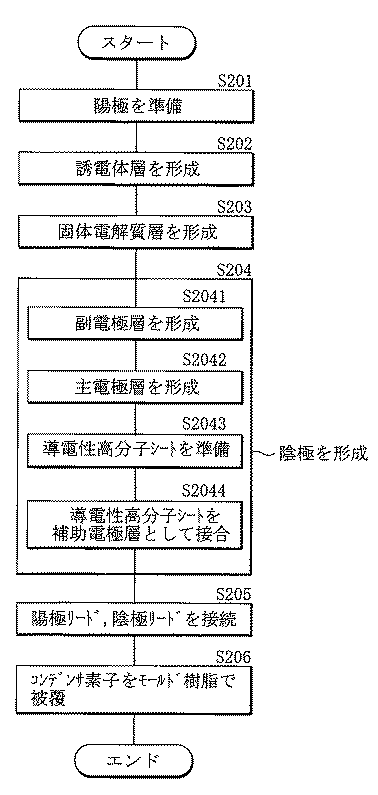
表1に示した結果から判るように、電解コンデンサの実使用上の諸特性として、ESRが100mΩ以下、漏れ電流が10.0μA以下、ならびに逆電圧試験がOKである条件(適性条件)が必要であるとすると、導電性粒子として金属粒子または導電性セラミック粒子を使用した実施例1〜7の電解コンデンサでは、ESR、漏れ電流および逆電圧試験の全てが適性条件を満たした。すなわち、実施例1〜7の電解コンデンサでは、(1)導電性粒子として金属粒子または導電性セラミック粒子を含んでいるため、それらの金属粒子または導電性セラミック粒子の低抵抗特性に基づいてESRが小さくなり、(2)製造途中において誘電体層に過度な外力が加わらず、その誘電体層が力学的要因に起因して破損しにくいために漏れ電流が小さくなり、(3)逆電圧を印加した際に瞬間的に過電流が流れたが、補助電極層のPTC機能を利用して陰極が高抵抗化することにより過電流が抑制されたため、発火または発煙等が生じなかった。これに対して、比較例1〜3の電解コンデンサでは、ESR、漏れ電流および逆電圧試験の一部が適性条件を満たさなかった。具体的には、比較例1,3の電解コンデンサでは、漏れ電流および逆電圧試験の双方が適性条件を満たした一方で、ESRが適性条件を満たさず、比較例2の電解コンデンサでは、逆電圧試験のみが適性条件を満たし、ESRおよび漏れ電流の双方が適性条件を満たさなかった。すなわち、比較例1〜3の電解コンデンサでは、導電性粒子として金属粒子または導電性粒子を含まずにカーボン粒子を含んでいるため、そのカーボン粒子の抵抗特性に起因していずれの電解コンデンサにおいてもESRが適性条件を満たさなかった。参考までに、比較例4の電解コンデンサでは、ESRおよび漏れ電流の双方が適性条件を満たしたものの、PTC機能を有していないないために逆電圧試験で発煙が生じた。これらのことから、実施例1〜7の電解コンデンサでは、ESRおよび漏れ電流の双方が抑制されると共に、発火や発煙などの不具合の発生が防止され、特に、それらの電解コンデンサの抵抗特性を低下させることが可能であることが確認された。 As can be seen from the results shown in Table 1, as the actual characteristics of the electrolytic capacitor, ESR is 100 mΩ or less, leakage current is 10.0 μA or less, and reverse voltage test is OK (appropriate condition). In the electrolytic capacitors of Examples 1 to 7 using metal particles or conductive ceramic particles as the conductive particles, the ESR, leakage current, and reverse voltage test all satisfied the suitability conditions. That is, in the electrolytic capacitors of Examples 1 to 7, since (1) the conductive particles include metal particles or conductive ceramic particles, ESR is based on the low resistance characteristics of the metal particles or conductive ceramic particles. (2) An excessive external force is not applied to the dielectric layer during the manufacturing process, and the dielectric layer is less likely to be damaged due to mechanical factors, so that the leakage current is reduced. (3) The reverse voltage is applied. In this case, an overcurrent flowed instantaneously. However, since the overcurrent was suppressed by increasing the resistance of the cathode using the PTC function of the auxiliary electrode layer, there was no ignition or smoke. In contrast, in the electrolytic capacitors of Comparative Examples 1 to 3, some of the ESR, leakage current, and reverse voltage tests did not satisfy the suitability conditions. Specifically, in the electrolytic capacitors of Comparative Examples 1 and 3, both the leakage current and the reverse voltage test satisfied the suitability conditions, while the ESR did not satisfy the suitability conditions. In the electrolytic capacitors of Comparative Example 2, the reverse voltage Only the test met the suitability condition, and both ESR and leakage current did not meet the suitability condition. That is, in the electrolytic capacitors of Comparative Examples 1 to 3, since the carbon particles are included as the conductive particles without including the metal particles or the conductive particles, in any electrolytic capacitor due to the resistance characteristics of the carbon particles. ESR did not meet suitability conditions. For reference, in the electrolytic capacitor of Comparative Example 4, although both the ESR and the leakage current satisfied the appropriate conditions, smoke was generated in the reverse voltage test because they did not have the PTC function. For these reasons, in the electrolytic capacitors of Examples 1 to 7, both ESR and leakage current are suppressed, and the occurrence of defects such as ignition and smoke is prevented, and in particular, the resistance characteristics of these electrolytic capacitors are reduced. It was confirmed that it was possible to
特に、実施例1〜7の電解コンデンサ間でESRを比較すると、補助電極層を形成するために接合(接着)処理を使用した実施例7の電解コンデンサよりも、塗布(硬化または乾燥)処理を使用した実施例1〜6の電解コンデンサにおいてESRがより低下した。すなわち、実施例1〜6の電解コンデンサでは、実施例7の電解コンデンサと比較して主電極層と補助電極層との間の接触抵抗が小さくなるため、その接触抵抗の低下分だけESRが小さくなった。これらのことから、実施例1〜6の電解コンデンサにおいて抵抗特性をより低下させることが可能であることが確認された。 In particular, when ESR is compared between the electrolytic capacitors of Examples 1 to 7, the coating (curing or drying) treatment is performed more than the electrolytic capacitor of Example 7 using a bonding (adhesion) treatment to form an auxiliary electrode layer. In the electrolytic capacitors of Examples 1 to 6 used, ESR was further reduced. That is, in the electrolytic capacitors of Examples 1 to 6, since the contact resistance between the main electrode layer and the auxiliary electrode layer is smaller than that of the electrolytic capacitor of Example 7, the ESR is decreased by the amount of decrease in the contact resistance. became. From these, it was confirmed that the resistance characteristics of the electrolytic capacitors of Examples 1 to 6 can be further reduced.
なお、具体的にデータを示した上で説明しないが、3層構造(副電極層,主電極層,補助電極層)を有する陰極のうちの補助電極層のみがPTC機能を有するように電解コンデンサを製造する代わりに、副電極層のみがPTC機能を有する電解コンデンサ、主電極層のみがPTC機能を有する電解コンデンサ、副電極層、主電極層および補助電極層のうちの任意の2つの組み合わせのみがPTC機能を有する電解コンデンサ、ならびに副電極層、主電極層および補助電極層の全てがPTC機能を有する電解コンデンサを製造して同様に諸特性を調べたところ、いずれの電解コンデンサにおいても実施例1〜7の電解コンデンサに関して得られた結果と同様の結果が得られた。このことから、陰極の構造にかかわらず、導電性粒子として金属粒子または導電性セラミック粒子を含むように陰極を形成することにより、電解コンデンサの抵抗特性を低下させることが可能であることが確認された。 Although not specifically described after showing data, an electrolytic capacitor so that only the auxiliary electrode layer of the cathode having a three-layer structure (sub-electrode layer, main electrode layer, auxiliary electrode layer) has a PTC function. Instead of manufacturing an electrolytic capacitor in which only the sub-electrode layer has a PTC function, an electrolytic capacitor in which only the main electrode layer has a PTC function, a combination of any two of the sub-electrode layer, the main electrode layer, and the auxiliary electrode layer Manufactured an electrolytic capacitor having a PTC function, and an electrolytic capacitor in which all of the sub electrode layer, the main electrode layer, and the auxiliary electrode layer had a PTC function, and various characteristics were examined in the same manner. Results similar to those obtained for the electrolytic capacitors 1-7 were obtained. From this, it was confirmed that the resistance characteristics of the electrolytic capacitor can be lowered by forming the cathode so as to include metal particles or conductive ceramic particles as the conductive particles regardless of the structure of the cathode. It was.
参考までに、実施例1〜7および比較例1〜3の陰極に関してPTC特性を調べたところ、表2に示した結果が得られた。表2は陰極のPTC特性を表しており、そのPTC特性として「室温抵抗(mΩ)」、「動作開始温度(℃)」および「抵抗変化率(桁数)」を示している。この「動作開始温度」は、25℃で示した抵抗値と比較して、その抵抗値の5倍の抵抗値を示した温度である。また、「抵抗変化率」は、抵抗の上昇桁数を表しており、すなわち室温抵抗R1とPTC機能に基づいて上昇した抵抗R2との間にR2=10x ×R1の関係が成立している場合の桁数xを表している。PTC特性を調べる際には、実施例1〜6および比較例3に関しては、補助電極層の形成材料(金属ペースト)を2枚の電解ニッケル箔電極(25μm厚)間において0.2mmの厚さとなるように膜化することにより電極付きPTCシートを作製し、直径10mmの円盤状に打ち抜いたのち、その電極付きPTCシートを恒温槽中に投入し、25℃〜160℃の範囲内において2℃/分で昇温させながら4端子法で2℃ごとに抵抗を測定した。一方、実施例7および比較例1,2に関しては、2枚の電解ニッケル箔電極間に導電性高分子シートを熱圧着した点を除いて実施例1〜6および比較例3の場合と同様の手順を経ることにより電極付きPTCシートを作製し、その電極付きPTCシートの抵抗を測定した。なお、表2には、参考までに、補助電極層の材料構成(液状高分子(膜状高分子),導電性粒子)を併せて示している。 For reference, when the PTC characteristics of the cathodes of Examples 1 to 7 and Comparative Examples 1 to 3 were examined, the results shown in Table 2 were obtained. Table 2 shows the PTC characteristics of the cathode. As the PTC characteristics, “room temperature resistance (mΩ)”, “operation start temperature (° C.)”, and “resistance change rate (number of digits)” are shown. This “operation start temperature” is a temperature indicating a resistance value five times that of the resistance value indicated at 25 ° C. Further, the “resistance change rate” represents the number of increasing digits of the resistance, that is, a relationship of R2 = 10 ×× R1 is established between the room temperature resistance R1 and the resistance R2 increased based on the PTC function. Represents the number of digits x. When examining the PTC characteristics, with respect to Examples 1 to 6 and Comparative Example 3, the auxiliary electrode layer forming material (metal paste) had a thickness of 0.2 mm between two electrolytic nickel foil electrodes (25 μm thick). After forming a PTC sheet with an electrode by forming into a film and punching out into a disk shape having a diameter of 10 mm, the PTC sheet with an electrode is put into a thermostatic bath, and the temperature is 2 ° C. within a range of 25 ° C. to 160 ° C. The resistance was measured every 2 ° C. by the 4-terminal method while raising the temperature at a rate of 1 minute. On the other hand, with respect to Example 7 and Comparative Examples 1 and 2, the same as in Examples 1 to 6 and Comparative Example 3 except that a conductive polymer sheet was thermocompression bonded between two electrolytic nickel foil electrodes. A PTC sheet with an electrode was prepared through the procedure, and the resistance of the PTC sheet with an electrode was measured. For reference, Table 2 also shows the material configuration of the auxiliary electrode layer (liquid polymer (film polymer), conductive particles).
表2に示した結果から判るように、実施例1〜7および比較例1〜3の陰極では、いずれの場合においても3桁以上の抵抗変化率が得られ、すなわち抵抗が1000倍以上に上昇した。このことから、実施例1〜7および比較例1〜3の陰極は、PTC機能を発揮し得るだけの十分な抵抗変化率を有していることが確認された。なお、具体的にデータを示した上で説明しないが、確認までに、PTC機能を有していないカーボンブラックペースト(実施例1〜7および比較例1〜3の副電極層)および同様にPTC機能を有していない銀ペースト(実施例1〜6および比較例1〜3の主電極層)の抵抗特性を調べ、具体的には、ディップ法を使用して30mm×30mm寸法のガラス板上に各ペーストを成膜(加熱・乾燥を含む)したのち、金属クリップで挟んで各ペーストの室温抵抗を測定すると共に、150℃の恒温槽中で同様に各ペーストの抵抗を測定したところ、各ペーストの抵抗の上昇率は20%以内に留まり、PTC機能を発揮し得るだけの十分な抵抗変化率が得られなかった。 As can be seen from the results shown in Table 2, in each of the cathodes of Examples 1 to 7 and Comparative Examples 1 to 3, a resistance change rate of 3 digits or more was obtained, that is, the resistance increased 1000 times or more. did. From this, it was confirmed that the cathodes of Examples 1 to 7 and Comparative Examples 1 to 3 have a sufficient resistance change rate that can exhibit the PTC function. In addition, although it does not explain after showing data concretely, by confirmation, the carbon black paste (sub electrode layer of Examples 1-7 and Comparative Examples 1-3) which does not have a PTC function, and PTC similarly The resistance characteristics of the silver paste having no function (the main electrode layers of Examples 1 to 6 and Comparative Examples 1 to 3) were examined. Specifically, on a glass plate having a size of 30 mm × 30 mm using the dip method After each paste was formed into a film (including heating and drying), the resistance of each paste was measured in a constant temperature bath at 150 ° C. The rate of increase in the resistance of the paste remained within 20%, and a sufficient resistance change rate that could exhibit the PTC function was not obtained.
以上、実施の形態および実施例を挙げて本発明を説明したが、本発明はこれらの実施の形態や実施例に限定されず、導電性粒子として金属粒子および導電性セラミック粒子のうちの少なくとも一方を含むように形成されたPTC機能を有する陰極を備える限り、電解コンデンサの構成、材質または寸法、ならびに電解コンデンサの製造手順等は自由に変更可能である。 The present invention has been described with reference to the embodiments and examples. However, the present invention is not limited to these embodiments and examples, and the conductive particles are at least one of metal particles and conductive ceramic particles. As long as the cathode having the PTC function formed so as to include the electrolytic capacitor, the configuration, material or dimensions of the electrolytic capacitor, the manufacturing procedure of the electrolytic capacitor, and the like can be freely changed.
本発明に係る電解コンデンサおよびその製造方法は、電気的反応を生じる主要部(コンデンサ素子)が固体材料(導電性高分子)を含んで構成された固体電解コンデンサおよびその製造方法に適用することが可能である。 The electrolytic capacitor and the manufacturing method thereof according to the present invention can be applied to a solid electrolytic capacitor in which a main part (capacitor element) that generates an electrical reaction includes a solid material (conductive polymer) and a manufacturing method thereof. Is possible.
10…コンデンサ素子、11…陽極、12…誘電体層、12H…細孔、13…固体電解質層、14…陰極、14A…副電極層、14B…主電極層、14C…補助電極層。
DESCRIPTION OF
Claims (14)
ことを特徴とする電解コンデンサ。 A second electrode that includes at least one of a first electrode layer, a dielectric layer, a solid electrolyte layer, metal particles, and conductive ceramic particles, and has a resistance that increases with an increase in temperature within a predetermined temperature range. And an electrode layer having a laminated structure in which the electrode layers are laminated in this order.
その2層以上の層のうちの少なくとも1つの層において、前記金属粒子および前記導電性セラミック粒子のうちの少なくとも一方を含むと共に所定の温度範囲内において温度の上昇に伴って抵抗が上昇する
ことを特徴とする請求項1記載の電解コンデンサ。 The second electrode layer has a laminated structure in which two or more layers are laminated;
In at least one of the two or more layers, including at least one of the metal particles and the conductive ceramic particles, the resistance increases as the temperature rises within a predetermined temperature range. The electrolytic capacitor according to claim 1.
導電性を確保するための主電極層と、
この主電極層と前記固体電解質層との間に配設され、前記主電極層を前記固体電解質層に電気的に接合させるための副電極層と、
前記主電極層を挟んで前記副電極層と反対側に配設され、前記金属粒子および前記導電性セラミック粒子のうちの少なくとも一方を含むと共に所定の温度範囲内において温度の上昇に伴って抵抗が上昇する補助電極層と、を含む3層構造を有している
ことを特徴とする請求項2記載の電解コンデンサ。 The second electrode layer comprises:
A main electrode layer for ensuring conductivity;
A sub-electrode layer disposed between the main electrode layer and the solid electrolyte layer for electrically bonding the main electrode layer to the solid electrolyte layer;
Located on the opposite side of the sub-electrode layer across the main electrode layer, includes at least one of the metal particles and the conductive ceramic particles, and has a resistance as the temperature rises within a predetermined temperature range. The electrolytic capacitor according to claim 2, wherein the electrolytic capacitor has a three-layer structure including a rising auxiliary electrode layer.
ことを特徴とする請求項3記載の電解コンデンサ。 The electrolytic capacitor according to claim 3, wherein the main electrode layer includes a metal, and the sub electrode layer includes carbon.
ことを特徴とする請求項1記載の電解コンデンサ。 The electrolytic capacitor according to claim 1, wherein the second electrode layer has a single-layer structure.
前記導電性セラミック粒子が、炭化タングステン(WC)、窒化チタン(TiN)、窒化ジルコニウム(ZrN)、窒化チタン(TiN)、ホウ化チタン(TiB2 )、ケイ化モリブデン(MoSi2 )およびホウ化タンタル(TaB2 )を含む群のうちの少なくとも1種である
ことを特徴とする請求項1ないし請求項5のいずれか1項に記載の電解コンデンサ。 The metal particles are nickel (Ni), copper (Cu), aluminum (Al), tungsten (W), molybdenum (Mo), zinc (Zn), cobalt (Co), platinum (Pt), gold (Au) and At least one of the group comprising silver (Ag);
The conductive ceramic particles include tungsten carbide (WC), titanium nitride (TiN), zirconium nitride (ZrN), titanium nitride (TiN), titanium boride (TiB 2 ), molybdenum silicide (MoSi 2 ), and tantalum boride. The electrolytic capacitor according to any one of claims 1 to 5, wherein the electrolytic capacitor is at least one selected from the group including (TaB 2 ).
前記第2の電極層が、前記液状高分子が膜化されることにより形成された膜状高分子と、その膜状高分子中に保持された前記金属粒子および前記導電性セラミック粒子のうちの少なくとも一方とを含んで構成されている
ことを特徴とする請求項1ないし請求項6のいずれか1項に記載の電解コンデンサ。 The material for increasing the resistance in response to an increase in temperature within a predetermined temperature range is a liquid polymer containing at least one of the metal particles and the conductive ceramic particles,
The second electrode layer includes a film-like polymer formed by forming the liquid polymer into a film, the metal particles held in the film-like polymer, and the conductive ceramic particles. The electrolytic capacitor according to any one of claims 1 to 6, wherein the electrolytic capacitor includes at least one of them.
ことを特徴とする請求項7記載の電解コンデンサ。 The electrolytic capacitor according to claim 7, wherein the liquid polymer includes at least one of a thermosetting polymer and a soluble thermoplastic polymer.
ことを特徴とする請求項1ないし請求項8のいずれか1項に記載の電解コンデンサ。 The electrolysis according to any one of claims 1 to 8, wherein the second electrode layer has a resistance increased by 1000 times or more in a temperature range of 60 ° C or higher and 150 ° C or lower. Capacitor.
前記誘電体層が、前記第1の電極層の表層が陽極酸化されることにより形成されたものである
ことを特徴とする請求項1ないし請求項9のいずれか1項に記載の電解コンデンサ。 The first electrode layer comprises a valve metal;
The electrolytic capacitor according to any one of claims 1 to 9, wherein the dielectric layer is formed by anodizing a surface layer of the first electrode layer.
ことを特徴とする電解コンデンサの製造方法。 On the solid electrolyte layer of the laminated structure in which the first electrode layer, the dielectric layer, and the solid electrolyte layer are laminated in this order, at least one of metal particles and conductive ceramic particles is included and a predetermined temperature range A method of manufacturing an electrolytic capacitor, wherein the second electrode layer is formed so that the resistance increases in response to an increase in temperature.
前記導電性セラミック粒子として、炭化タングステン(WC)、窒化チタン(TiN)、窒化ジルコニウム(ZrN)、窒化チタン(TiN)、ホウ化チタン(TiB2 )、ケイ化モリブデン(MoSi2 )およびホウ化タンタル(TaB2 )を含む群のうちの少なくとも1種を使用する
ことを特徴とする請求項11記載の電解コンデンサの製造方法。 As the metal particles, nickel (Ni), copper (Cu), aluminum (Al), tungsten (W), molybdenum (Mo), zinc (Zn), cobalt (Co), platinum (Pt), gold (Au) and Using at least one of the group comprising silver (Ag),
Examples of the conductive ceramic particles include tungsten carbide (WC), titanium nitride (TiN), zirconium nitride (ZrN), titanium nitride (TiN), titanium boride (TiB 2 ), molybdenum silicide (MoSi 2 ), and tantalum boride. The method for producing an electrolytic capacitor according to claim 11, wherein at least one selected from the group including (TaB 2 ) is used.
その液状高分子が膜化した膜状高分子と、その膜状高分子中に保持された前記金属粒子および前記導電性セラミック粒子のうちの少なくとも一方とを含むように、前記第2の電極層を形成する
ことを特徴とする請求項11または請求項12に記載の電解コンデンサの製造方法。 Using a liquid polymer containing at least one of the metal particles and the conductive ceramic particles as a material for increasing resistance in response to an increase in temperature within a predetermined temperature range,
The second electrode layer so as to include a film polymer in which the liquid polymer is formed, and at least one of the metal particles and the conductive ceramic particles held in the film polymer. The method for manufacturing an electrolytic capacitor according to claim 11, wherein the electrolytic capacitor is formed.
ことを特徴とする請求項13記載の電解コンデンサの製造方法。 The method for producing an electrolytic capacitor according to claim 13, wherein at least one of a thermosetting polymer and a soluble thermoplastic polymer is used as the liquid polymer.
Priority Applications (3)
| Application Number | Priority Date | Filing Date | Title |
|---|---|---|---|
| JP2004107215A JP2005294522A (en) | 2004-03-31 | 2004-03-31 | Electrolytic capacitor and its manufacturing method |
| US11/089,227 US7218506B2 (en) | 2004-03-31 | 2005-03-25 | Electrolytic capacitor and method of manufacturing the same |
| US11/634,126 US7245479B2 (en) | 2004-03-31 | 2006-12-06 | Electrolytic capacitor and method of manufacturing the same |
Applications Claiming Priority (1)
| Application Number | Priority Date | Filing Date | Title |
|---|---|---|---|
| JP2004107215A JP2005294522A (en) | 2004-03-31 | 2004-03-31 | Electrolytic capacitor and its manufacturing method |
Publications (1)
| Publication Number | Publication Date |
|---|---|
| JP2005294522A true JP2005294522A (en) | 2005-10-20 |
Family
ID=35327116
Family Applications (1)
| Application Number | Title | Priority Date | Filing Date |
|---|---|---|---|
| JP2004107215A Pending JP2005294522A (en) | 2004-03-31 | 2004-03-31 | Electrolytic capacitor and its manufacturing method |
Country Status (1)
| Country | Link |
|---|---|
| JP (1) | JP2005294522A (en) |
Cited By (1)
| Publication number | Priority date | Publication date | Assignee | Title |
|---|---|---|---|---|
| CN116814044A (en) * | 2023-06-06 | 2023-09-29 | 浙江工业大学 | Epoxy resin composite insulating material and preparation method and application thereof |
-
2004
- 2004-03-31 JP JP2004107215A patent/JP2005294522A/en active Pending
Cited By (1)
| Publication number | Priority date | Publication date | Assignee | Title |
|---|---|---|---|---|
| CN116814044A (en) * | 2023-06-06 | 2023-09-29 | 浙江工业大学 | Epoxy resin composite insulating material and preparation method and application thereof |
Similar Documents
| Publication | Publication Date | Title |
|---|---|---|
| US7218506B2 (en) | Electrolytic capacitor and method of manufacturing the same | |
| TWI478189B (en) | Solid electrolytic capacitor and method of manufacturing thereof | |
| US7060205B2 (en) | Solid electrolytic capacitor and method for producing the same | |
| CN101484958B (en) | Solid electrolytic capacitor | |
| JP4600398B2 (en) | Solid electrolytic capacitor and manufacturing method thereof | |
| US6999303B2 (en) | Solid electrolytic capacitor and process for its fabrication | |
| JP2003059763A (en) | Method of manufacturing solid electrolytic capacitor | |
| JP7752360B2 (en) | Solid electrolytic capacitor element and solid electrolytic capacitor | |
| WO2018043063A1 (en) | Electrolytic capacitor and method for producing same | |
| JP5321964B2 (en) | Solid electrolytic capacitor and manufacturing method thereof | |
| JP4539141B2 (en) | Electrolytic capacitor and manufacturing method thereof | |
| JP2000021687A (en) | Capacitor and manufacturing method thereof | |
| JP2005294522A (en) | Electrolytic capacitor and its manufacturing method | |
| JP3356018B2 (en) | Capacitor and manufacturing method thereof | |
| JP2003289015A (en) | Polymer solid electrolytic capacitor | |
| JP2005294420A (en) | Electrolytic capacitor or its manufacturing method | |
| JP2012153867A (en) | Conductive composition as well as production method therefor, and capacitor prepared using the conductive composition | |
| JP2007123315A (en) | Manufacturing method of redox capacitor electrode, redox capacitor electrode obtained thereby and redox capacitor | |
| JP4937170B2 (en) | Solid electrolytic capacitor | |
| JP2005294507A (en) | Electrolytic capacitor and its manufacturing method | |
| JP3551118B2 (en) | Capacitor and manufacturing method thereof | |
| JP2005135853A (en) | Solid electrolyte, electrolytic capacitor and its manufacturing method | |
| JP2006135191A (en) | Solid electrolytic capacitor and manufacturing method thereof | |
| JP2005191126A (en) | Method for forming conductive polymer, and method for producing electronic component | |
| JP2005136336A (en) | Solid electrolyte and its manufacturing method, and electrolytic capacitor and its manufacturing method |
Legal Events
| Date | Code | Title | Description |
|---|---|---|---|
| A621 | Written request for application examination |
Free format text: JAPANESE INTERMEDIATE CODE: A621 Effective date: 20061116 |
|
| A977 | Report on retrieval |
Free format text: JAPANESE INTERMEDIATE CODE: A971007 Effective date: 20090910 |
|
| A131 | Notification of reasons for refusal |
Free format text: JAPANESE INTERMEDIATE CODE: A131 Effective date: 20090916 |
|
| A02 | Decision of refusal |
Free format text: JAPANESE INTERMEDIATE CODE: A02 Effective date: 20100126 |