JP2005294469A - Hall element mounting method - Google Patents
Hall element mounting method Download PDFInfo
- Publication number
- JP2005294469A JP2005294469A JP2004106265A JP2004106265A JP2005294469A JP 2005294469 A JP2005294469 A JP 2005294469A JP 2004106265 A JP2004106265 A JP 2004106265A JP 2004106265 A JP2004106265 A JP 2004106265A JP 2005294469 A JP2005294469 A JP 2005294469A
- Authority
- JP
- Japan
- Prior art keywords
- hall element
- substrate
- reduced
- lands
- glass epoxy
- Prior art date
- Legal status (The legal status is an assumption and is not a legal conclusion. Google has not performed a legal analysis and makes no representation as to the accuracy of the status listed.)
- Pending
Links
Images


Landscapes
- Measuring Magnetic Variables (AREA)
- Hall/Mr Elements (AREA)
Abstract
【課題】ハンダリフロー法により基板へハンダ付けしたホール素子が、基板の収縮応力を受けて座屈することを防止する。
【解決手段】ガラスエポキシ基板3のホール素子ハンダ付け用の四つのランド4の中央に円穴5を形成する。ハンダリフロー工程において基板が加熱されたときに穴の部分は逃げとして働くことから、ランドのピッチ変化は低減し、熱膨張係数の小さいホール素子1の電極端子2との相対的なピッチ差も縮小する。又、基板自体のバネとしての定数が低下するので、ハンダ付け後に基板が収縮する際にホール素子にかかる収縮応力が低減し、ホール素子の座屈度や変形度が低減する。
【選択図】 図1
A Hall element soldered to a substrate by a solder reflow method is prevented from buckling due to contraction stress of the substrate.
A circular hole 5 is formed at the center of four lands 4 for soldering a Hall element on a glass epoxy substrate 3. Since the hole part works as a relief when the substrate is heated in the solder reflow process, the pitch change of the land is reduced, and the relative pitch difference with the electrode terminal 2 of the Hall element 1 having a small thermal expansion coefficient is also reduced. To do. Further, since the constant of the substrate itself as a spring is reduced, the contraction stress applied to the Hall element when the substrate contracts after soldering is reduced, and the buckling degree and deformation degree of the Hall element are reduced.
[Selection] Figure 1
Description
この発明は、ホール素子の搭載方法に関するものであり、特に、性能の安定化を図ったホール素子の搭載方法に関するものである。 The present invention relates to a method for mounting a Hall element, and more particularly to a method for mounting a Hall element in which performance is stabilized.
ロータの回転数や回転角度の検出や、ポインティングデバイスの操作量検出の手段として、ホール素子或いはホール素子に加えて増幅器などを一体化したホールICが広く一般に用いられている(例えば、特許文献1、特許文献2など)。ホール素子は、リード線を備えたもののほかに、樹脂やセラミックのパッケージに封入され、パッケージから端子ピンが突出しているSIP型やDIP型のものや、ピンレスのチップ型のものがあり、これらのリードレス型パッケージ部品はハンダリフロー法によって基板上に実装される。 As a means for detecting the number of rotations and rotation angle of the rotor and detecting the operation amount of the pointing device, a Hall IC in which an amplifier or the like is integrated in addition to the Hall element or the Hall element is widely used (for example, Patent Document 1). Patent Document 2). In addition to those with lead wires, Hall elements are encapsulated in resin or ceramic packages, and there are SIP and DIP types with terminal pins protruding from the package, and pinless chip types. The leadless package component is mounted on a substrate by a solder reflow method.
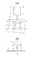
従来のリードレス型ホール素子の搭載方法を図8に示す。尚、ここではホール素子とホールICの両方をホール素子と総称することとする。1はチップ型のホール素子であり、パッケージの底面の四隅にそれぞれ電極端子2が配置されている。ホール素子1を搭載するガラスエポキシ基板3には、ホール素子1の四つの電極端子2に対応する四つのランド4が設けられており、ホール素子1の電極端子2をガラスエポキシ基板3のランド4に載せた状態でハンダリフロー装置にかけてホール素子1の電極端子2とガラスエポキシ基板3のランド4をハンダ付けする。
A conventional method for mounting a leadless Hall element is shown in FIG. Here, both the Hall element and the Hall IC are collectively referred to as a Hall element.
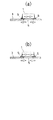
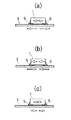
このとき、ハンダリフロー装置内でホール素子とガラスエポキシ基板がハンダ共晶温度以上に加熱され、ハンダSが溶融した後に放熱冷却されてホール素子と基板がハンダ付けされる。しかし、ホール素子とガラスエポキシ基板の膨張係数は異なっていて、ガラスエポキシ基板の膨張係数のほうが大きいことから、図9(a)に示すようにそれぞれ膨張した状態でハンダ付けされた後の収縮率が異なり、ホール素子1よりも大きく収縮するガラスエポキシ基板3の収縮応力により、放熱後は図9(b)に示すようにホール素子1が座屈或いは圧縮変形して固定されることなる。
At this time, the Hall element and the glass epoxy substrate are heated to a temperature equal to or higher than the solder eutectic temperature in the solder reflow apparatus, and after the solder S is melted, heat radiation is cooled and the Hall element and the substrate are soldered. However, since the expansion coefficient of the Hall element and the glass epoxy substrate are different and the expansion coefficient of the glass epoxy substrate is larger, the shrinkage rate after soldering in the expanded state as shown in Fig. 9 (a) However, due to the contraction stress of the
これにより、ホール素子にピエゾ効果による抵抗値の増加が生じ、ブリッジ抵抗が不整合となって出力に異常をきたすことがある。また、ハンダ付け後から時間が経過するとともに、引張り応力がかかっているハンダSがクリープ変形して、図9(c)に示すようにガラスエポキシ基板3とホール素子1も徐々に原型に復帰する傾向をもち、ホール素子1に作用しているピエゾ効果が低減し、内部の抵抗値が減少して初期値に近づき、基板のバネ力がハンダの弾性応力域にまで減るとクリープは止まる。つまり、ホール素子の入力/出力特性が時間とともに変化するという不都合が生じる。
ハンダリフロー法によるホール素子の搭載方法は、ホール素子の変形や座屈による内部抵抗値の増加をもたらして、電磁変換性能が悪化することがある。特に、近年は環境負荷を低減するために機器の無鉛化(鉛フリー化)が要求されており、比較的共晶温度が高い鉛フリーハンダを使用する場合は、リフロー工程における温度がより高温化して、基板の熱膨張量も大きくなり、上述した問題が顕在化することが確認されている。 The mounting method of the Hall element by the solder reflow method may increase the internal resistance value due to deformation or buckling of the Hall element, and may deteriorate the electromagnetic conversion performance. In particular, in recent years, there has been a demand for lead-free (lead-free) equipment in order to reduce environmental impact. When lead-free solder with a relatively high eutectic temperature is used, the temperature in the reflow process has become higher. As a result, the amount of thermal expansion of the substrate also increases, and it has been confirmed that the above-described problems become apparent.
そこで、ホール素子を基盤へハンダ付けする場合において、ホール素子にかかる応力を低減して、内部抵抗の不整合による出力異常、及び入力/出力特性の経時変化を解消するために解決すべき技術的課題が生じてくるのであり、本発明は上記課題を解決することを目的とする。 Therefore, when soldering the Hall element to the substrate, the technical to be solved to reduce the stress applied to the Hall element and eliminate the output abnormality due to mismatch of internal resistance and the change of input / output characteristics over time Problems arise, and the present invention aims to solve the above problems.
この発明は、上記目的を達成するために提案するものであり、基板に設けた複数のランドへホール素子をハンダリフロー法によりハンダ付けするホール素子の搭載方法において、基板のホール素子搭載位置に穴を形成し、基板加熱時におけるランドピッチの変動を抑制し、ホール素子に掛かる応力を低減することを特徴とするホール素子の搭載方法を提供するものである。 The present invention is proposed in order to achieve the above object, and in a mounting method of a Hall element, in which a Hall element is soldered to a plurality of lands provided on a substrate by a solder reflow method, a hole is formed at the Hall element mounting position of the substrate. The Hall element mounting method is characterized in that a variation in land pitch during substrate heating is suppressed, and stress applied to the Hall element is reduced.
また、上記基板の複数のランドで囲まれる領域の中央に穴を形成して、ホール素子を搭載するホール素子の搭載方法を提供するものである。 Further, the present invention provides a method for mounting a Hall element, in which a hole is formed in the center of a region surrounded by a plurality of lands on the substrate.
また、上記基板の隣り合うランドの間にそれぞれ穴を形成して、ホール素子を搭載するホール素子の搭載方法を提供するものである。 Further, the present invention provides a method for mounting a Hall element, in which holes are formed between adjacent lands of the substrate, respectively.
上記の構成では、ハンダリフロー工程において基板が加熱されたときに穴の部分は逃げとして働くことから、ランドのピッチ変化は低減し、熱膨張係数の小さいホール素子の端子との相対的なピッチ差も縮小することになる。又、基板自体のバネとしての定数が低下するので、ハンダ付け後に基板が収縮する際にホール素子にかかる収縮応力が低減し、ホール素子の座屈度や変形度が低減する。 In the above configuration, when the substrate is heated in the solder reflow process, the hole portion acts as a relief, so that the land pitch change is reduced and the relative pitch difference with the terminal of the Hall element having a small thermal expansion coefficient. Will also be reduced. Further, since the constant of the substrate itself as a spring is reduced, the contraction stress applied to the Hall element when the substrate contracts after soldering is reduced, and the buckling degree and deformation degree of the Hall element are reduced.
この発明は、ホール素子が搭載される基板の複数のランド間に穴を設けることにより、ハンダリフロー法によるハンダ付けの際の基板膨張量を抑制し、基板とホール素子の熱膨張係数の相違によるハンダ付け後のホール素子の座屈や変形を低減した。これによりハンダ付け後のホール素子の出力異常や入力/出力特性の経時変化を低減でき、電気的性能が安定化する。 In the present invention, by providing holes between a plurality of lands of the substrate on which the Hall element is mounted, the amount of expansion of the substrate when soldering by the solder reflow method is suppressed, and the difference in thermal expansion coefficient between the substrate and the Hall element is caused. Reduced buckling and deformation of hall elements after soldering. As a result, the output abnormality of the Hall element after soldering and the change over time of the input / output characteristics can be reduced, and the electrical performance is stabilized.
この発明は、基板のホール素子搭載位置に穴を設けて、ハンダ付けの際の加熱により基板のランドピッチが変動することを抑制することにより、ハンダ付け後の基板の収縮によりホール素子に加わる応力を可及的に軽減して、ホール素子の変形や電気特性の経時変化を防止する目的を達成した。 According to the present invention, a hole is provided at the Hall element mounting position of the substrate, and the stress applied to the Hall element due to shrinkage of the substrate after soldering is suppressed by suppressing fluctuation of the land pitch of the substrate due to heating during soldering. As much as possible, the purpose of preventing deformation of the Hall element and changes in electrical characteristics over time has been achieved.
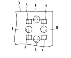
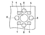
図1において、1はチップ型のホール素子、3はガラスエポキシ基板である。ホール素子のパッケージの底面四隅にはそれぞれ電極端子2が配置されており、ホール素子1を搭載するガラスエポキシ基板3には、ホール素子1の四つの電極端子2に対応する四つのランド4が設けられている。ホール素子1は、電極端子2をガラスエポキシ基板3のランド4に位置合わせしてガラスエポキシ基板3に載せられ、ハンダリフロー装置にかけて電極端子2とガラスエポキシ基板3のランド4をハンダ付けするのであるが、本発明の要旨は、ガラスエポキシ基板3に設けられている四つのランド4の間に穴を形成していることにあり、ここでは、四つのランド4の中央に円穴5を形成している。
In FIG. 1, 1 is a chip-type Hall element, and 3 is a glass epoxy substrate.
つまり、ホール素子1を搭載する領域に円穴5を設けたことにより、ガラスエポキシ基板3が加熱されて膨張するときに円穴5の部分は逃げとして働き、四つのランド4のピッチ変化は穴の無い場合に比して低減する。ホール素子1のパッケージの熱膨張係数は小さいので、図2(a)に示すように、ガラスエポキシ基板3のランド4にホール素子1を載せてハンダリフロー装置にかけて加熱したときに、ホール素子1の電極端子2のピッチとガラスエポキシ基板3のランド4のピッチ差不整合は抑制される。
In other words, by providing the
これにより、ハンダリフロー工程が終了して温度が低下し、図2(b)に示すようにガラスエポキシ基板3とホール素子1が収縮したときにも、ホール素子1の電極端子間ピッチとガラスエポキシ基板3の不整合は低減するので、ガラスエポキシ基板3からのホール素子1への応力は減り、ホール素子1の圧縮変形及び座屈が抑制される。
As a result, when the solder reflow process is completed and the temperature drops and the
基板に設ける穴の形状は、実施例1の円穴に限らず、基板加熱時にランドピッチの膨張を軽減するという目的を達成できるものであればよく、図3のように方形の穴6を対角線方向に向けて配置してもよく、図4のように十字型の穴7であってもよい。 The shape of the hole provided in the substrate is not limited to the circular hole in the first embodiment, and any shape can be used as long as it can achieve the purpose of reducing the expansion of the land pitch when the substrate is heated. As shown in FIG. It may be arranged in the direction, or may be a cross-shaped hole 7 as shown in FIG.
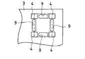
また、基板のホール素子搭載位置の中央に穴を配置するものに代えて、図5に示すように、隣り合うランド4の間にそれぞれ円穴8を配置してもよく、図6に示すように隣り合うランド4の間にそれぞれ長穴9を配置してもよい。
また、図1乃至図4の中央配置の構成に図5乃至図6のランド間配置の構成を加えて、図7に示すように、四つのランドの中央と、隣り合うランドの間にそれぞれ円穴5, 8や角穴を配置してもよい。また、上記実施形態では、基板としてガラスエポキシ基板を用いた例を述べたが、紙フェノール基板や鉄基板など他種の基板であっても本発明を適用でき、基板の材質は問わないことは言うまでもない。
Further, instead of the hole arranged at the center of the Hall element mounting position on the substrate, as shown in FIG. 5,
In addition, the inter-land arrangement shown in FIGS. 5 to 6 is added to the central arrangement shown in FIGS. 1 to 4, and as shown in FIG. 7, a circle is formed between the center of the four lands and adjacent lands.
尚、この発明は上記の実施形態に限定するものではなく、この発明の技術的範囲内において種々の改変が可能であり、この発明がそれらの改変されたものに及ぶことは当然である。 The present invention is not limited to the above-described embodiment, and various modifications are possible within the technical scope of the present invention, and it is natural that the present invention extends to those modifications.
1 ホール素子
2 電極端子
3 ガラスエポキシ基板
4 ランド
5 円穴
6 方形の穴
7 十字型の穴
8 円穴
9 長穴
1 Hall element
2 Electrode terminal
3 Glass epoxy board
4 rand
5 circle hole
6 square holes
7 Cross-shaped hole
8 round hole
9 Slotted hole
Claims (3)
2. The Hall element mounting method according to claim 1, wherein holes are formed by forming holes between adjacent lands of the substrate.
Priority Applications (1)
| Application Number | Priority Date | Filing Date | Title |
|---|---|---|---|
| JP2004106265A JP2005294469A (en) | 2004-03-31 | 2004-03-31 | Hall element mounting method |
Applications Claiming Priority (1)
| Application Number | Priority Date | Filing Date | Title |
|---|---|---|---|
| JP2004106265A JP2005294469A (en) | 2004-03-31 | 2004-03-31 | Hall element mounting method |
Publications (1)
| Publication Number | Publication Date |
|---|---|
| JP2005294469A true JP2005294469A (en) | 2005-10-20 |
Family
ID=35327075
Family Applications (1)
| Application Number | Title | Priority Date | Filing Date |
|---|---|---|---|
| JP2004106265A Pending JP2005294469A (en) | 2004-03-31 | 2004-03-31 | Hall element mounting method |
Country Status (1)
| Country | Link |
|---|---|
| JP (1) | JP2005294469A (en) |
Cited By (1)
| Publication number | Priority date | Publication date | Assignee | Title |
|---|---|---|---|---|
| CN113161477A (en) * | 2020-01-22 | 2021-07-23 | 株式会社东芝 | Chip package |
-
2004
- 2004-03-31 JP JP2004106265A patent/JP2005294469A/en active Pending
Cited By (3)
| Publication number | Priority date | Publication date | Assignee | Title |
|---|---|---|---|---|
| CN113161477A (en) * | 2020-01-22 | 2021-07-23 | 株式会社东芝 | Chip package |
| JP2021117004A (en) * | 2020-01-22 | 2021-08-10 | 株式会社東芝 | Chip package |
| JP7596070B2 (en) | 2020-01-22 | 2024-12-09 | 株式会社東芝 | Chip Package |
Similar Documents
| Publication | Publication Date | Title |
|---|---|---|
| US8599571B2 (en) | Memory card | |
| JP5417572B2 (en) | Chip resistor and manufacturing method thereof | |
| KR20010098931A (en) | Semiconductor device using bumps, method for fabricating same, and method for forming bumps | |
| WO2009116517A1 (en) | Electronic device and method for manufacturing the same | |
| WO2019073734A1 (en) | Electronic control device | |
| CN101964334B (en) | Semiconductor package and semiconductor package module | |
| JP6015242B2 (en) | Semiconductor device and circuit board | |
| US7247945B2 (en) | Semiconductor apparatus | |
| US5849609A (en) | Semiconductor package and a method of manufacturing thereof | |
| JP2005294469A (en) | Hall element mounting method | |
| EP2278864A1 (en) | Substrate, structure for mounting surface mounting component, and electronic device | |
| KR102156148B1 (en) | Low thermal stress package for large area semiconductor dies | |
| US20050029658A1 (en) | Circuit board and semiconductor device using the same | |
| JP5000621B2 (en) | Semiconductor device | |
| US20100053923A1 (en) | Semiconductor device and circuit board assembly | |
| JP3957694B2 (en) | Semiconductor package and system module | |
| EP3958300B1 (en) | External terminal for semiconductor module | |
| KR101725107B1 (en) | a structure of ring solder pad for enhanced reliability of semiconductor chip packaging | |
| JP2001127113A (en) | Mounting structure for surface mount semiconductor device | |
| JP2018107302A (en) | Semiconductor device | |
| US20140120661A1 (en) | Flip chip packaging method | |
| KR20080036345A (en) | Semiconductor package with solder balls | |
| JP2021158240A (en) | Electronic device | |
| JP2019508908A (en) | Packaging structure with solder balls and method of manufacturing the packaging structure | |
| JP2003324125A (en) | Semiconductor device |