JP2005294290A - Multilayered ceramic capacitor - Google Patents
Multilayered ceramic capacitor Download PDFInfo
- Publication number
- JP2005294290A JP2005294290A JP2004102423A JP2004102423A JP2005294290A JP 2005294290 A JP2005294290 A JP 2005294290A JP 2004102423 A JP2004102423 A JP 2004102423A JP 2004102423 A JP2004102423 A JP 2004102423A JP 2005294290 A JP2005294290 A JP 2005294290A
- Authority
- JP
- Japan
- Prior art keywords
- mol
- subcomponent
- dielectric
- ceramic capacitor
- multilayer ceramic
- Prior art date
- Legal status (The legal status is an assumption and is not a legal conclusion. Google has not performed a legal analysis and makes no representation as to the accuracy of the status listed.)
- Withdrawn
Links
- 239000003985 ceramic capacitor Substances 0.000 title claims abstract description 68
- 239000000203 mixture Substances 0.000 claims abstract description 29
- JRPBQTZRNDNNOP-UHFFFAOYSA-N barium titanate Chemical compound [Ba+2].[Ba+2].[O-][Ti]([O-])([O-])[O-] JRPBQTZRNDNNOP-UHFFFAOYSA-N 0.000 claims abstract description 24
- 229910002113 barium titanate Inorganic materials 0.000 claims abstract description 24
- 239000013078 crystal Substances 0.000 claims abstract description 16
- 229910052691 Erbium Inorganic materials 0.000 claims abstract description 8
- 229910052689 Holmium Inorganic materials 0.000 claims abstract description 7
- 229910052692 Dysprosium Inorganic materials 0.000 claims abstract description 6
- 229910052727 yttrium Inorganic materials 0.000 claims abstract description 6
- 239000002245 particle Substances 0.000 claims description 104
- 239000000919 ceramic Substances 0.000 claims description 20
- VYPSYNLAJGMNEJ-UHFFFAOYSA-N Silicium dioxide Chemical compound O=[Si]=O VYPSYNLAJGMNEJ-UHFFFAOYSA-N 0.000 claims description 4
- 229910052814 silicon oxide Inorganic materials 0.000 claims description 4
- 239000000463 material Substances 0.000 abstract description 6
- 230000002829 reductive effect Effects 0.000 abstract description 4
- 229910052573 porcelain Inorganic materials 0.000 abstract description 2
- 239000010410 layer Substances 0.000 description 95
- 238000010304 firing Methods 0.000 description 27
- 238000000034 method Methods 0.000 description 19
- 239000007789 gas Substances 0.000 description 17
- 238000000137 annealing Methods 0.000 description 16
- 239000003989 dielectric material Substances 0.000 description 15
- PXHVJJICTQNCMI-UHFFFAOYSA-N nickel Substances [Ni] PXHVJJICTQNCMI-UHFFFAOYSA-N 0.000 description 15
- 238000005245 sintering Methods 0.000 description 15
- 230000000694 effects Effects 0.000 description 14
- 239000011230 binding agent Substances 0.000 description 13
- 239000003990 capacitor Substances 0.000 description 13
- 229910052759 nickel Inorganic materials 0.000 description 9
- 239000007858 starting material Substances 0.000 description 9
- 239000004020 conductor Substances 0.000 description 8
- 238000001816 cooling Methods 0.000 description 8
- XLYOFNOQVPJJNP-UHFFFAOYSA-N water Substances O XLYOFNOQVPJJNP-UHFFFAOYSA-N 0.000 description 8
- 229910000990 Ni alloy Inorganic materials 0.000 description 7
- QVGXLLKOCUKJST-UHFFFAOYSA-N atomic oxygen Chemical compound [O] QVGXLLKOCUKJST-UHFFFAOYSA-N 0.000 description 7
- 238000009413 insulation Methods 0.000 description 7
- 229910052760 oxygen Inorganic materials 0.000 description 7
- 239000001301 oxygen Substances 0.000 description 7
- 230000036961 partial effect Effects 0.000 description 7
- 239000000470 constituent Substances 0.000 description 6
- 230000005684 electric field Effects 0.000 description 6
- LIVNPJMFVYWSIS-UHFFFAOYSA-N silicon monoxide Chemical compound [Si-]#[O+] LIVNPJMFVYWSIS-UHFFFAOYSA-N 0.000 description 6
- 229910052712 strontium Inorganic materials 0.000 description 6
- OAYXUHPQHDHDDZ-UHFFFAOYSA-N 2-(2-butoxyethoxy)ethanol Chemical compound CCCCOCCOCCO OAYXUHPQHDHDDZ-UHFFFAOYSA-N 0.000 description 5
- 229910052788 barium Inorganic materials 0.000 description 5
- 239000010953 base metal Substances 0.000 description 5
- 229910052726 zirconium Inorganic materials 0.000 description 5
- CSCPPACGZOOCGX-UHFFFAOYSA-N Acetone Chemical compound CC(C)=O CSCPPACGZOOCGX-UHFFFAOYSA-N 0.000 description 4
- 229910045601 alloy Inorganic materials 0.000 description 4
- 239000000956 alloy Substances 0.000 description 4
- 229910052791 calcium Inorganic materials 0.000 description 4
- 230000007423 decrease Effects 0.000 description 4
- 239000002003 electrode paste Substances 0.000 description 4
- 238000011156 evaluation Methods 0.000 description 4
- 238000005498 polishing Methods 0.000 description 4
- 239000010936 titanium Substances 0.000 description 4
- 229910052719 titanium Inorganic materials 0.000 description 4
- 229910018072 Al 2 O 3 Inorganic materials 0.000 description 3
- YMWUJEATGCHHMB-UHFFFAOYSA-N Dichloromethane Chemical compound ClCCl YMWUJEATGCHHMB-UHFFFAOYSA-N 0.000 description 3
- XEKOWRVHYACXOJ-UHFFFAOYSA-N Ethyl acetate Chemical compound CCOC(C)=O XEKOWRVHYACXOJ-UHFFFAOYSA-N 0.000 description 3
- 239000001856 Ethyl cellulose Substances 0.000 description 3
- ZZSNKZQZMQGXPY-UHFFFAOYSA-N Ethyl cellulose Chemical compound CCOCC1OC(OC)C(OCC)C(OCC)C1OC1C(O)C(O)C(OC)C(CO)O1 ZZSNKZQZMQGXPY-UHFFFAOYSA-N 0.000 description 3
- -1 MgO—Y Inorganic materials 0.000 description 3
- YXFVVABEGXRONW-UHFFFAOYSA-N Toluene Chemical compound CC1=CC=CC=C1 YXFVVABEGXRONW-UHFFFAOYSA-N 0.000 description 3
- 238000009826 distribution Methods 0.000 description 3
- 229920001249 ethyl cellulose Polymers 0.000 description 3
- 235000019325 ethyl cellulose Nutrition 0.000 description 3
- 238000004519 manufacturing process Methods 0.000 description 3
- 238000005259 measurement Methods 0.000 description 3
- 229910052751 metal Inorganic materials 0.000 description 3
- 239000002184 metal Substances 0.000 description 3
- 239000003960 organic solvent Substances 0.000 description 3
- 239000003973 paint Substances 0.000 description 3
- 239000000843 powder Substances 0.000 description 3
- 238000012545 processing Methods 0.000 description 3
- 239000002994 raw material Substances 0.000 description 3
- 239000000758 substrate Substances 0.000 description 3
- 239000004925 Acrylic resin Substances 0.000 description 2
- 229920000178 Acrylic resin Polymers 0.000 description 2
- 229920002799 BoPET Polymers 0.000 description 2
- 101100513612 Microdochium nivale MnCO gene Proteins 0.000 description 2
- 229910001252 Pd alloy Inorganic materials 0.000 description 2
- 229910052797 bismuth Inorganic materials 0.000 description 2
- 229910052796 boron Inorganic materials 0.000 description 2
- 230000015556 catabolic process Effects 0.000 description 2
- 239000002131 composite material Substances 0.000 description 2
- 150000001875 compounds Chemical class 0.000 description 2
- 229910052802 copper Inorganic materials 0.000 description 2
- 230000007547 defect Effects 0.000 description 2
- 238000000113 differential scanning calorimetry Methods 0.000 description 2
- 239000002270 dispersing agent Substances 0.000 description 2
- 238000002474 experimental method Methods 0.000 description 2
- 238000010438 heat treatment Methods 0.000 description 2
- 238000004898 kneading Methods 0.000 description 2
- 229910052745 lead Inorganic materials 0.000 description 2
- 230000000670 limiting effect Effects 0.000 description 2
- 229910052744 lithium Inorganic materials 0.000 description 2
- 150000002739 metals Chemical class 0.000 description 2
- 150000002902 organometallic compounds Chemical class 0.000 description 2
- 230000003647 oxidation Effects 0.000 description 2
- 238000007254 oxidation reaction Methods 0.000 description 2
- 229910052763 palladium Inorganic materials 0.000 description 2
- 229920000139 polyethylene terephthalate Polymers 0.000 description 2
- 239000005020 polyethylene terephthalate Substances 0.000 description 2
- 230000000630 rising effect Effects 0.000 description 2
- 238000005488 sandblasting Methods 0.000 description 2
- 229910052709 silver Inorganic materials 0.000 description 2
- 238000010532 solid phase synthesis reaction Methods 0.000 description 2
- 238000012360 testing method Methods 0.000 description 2
- 229910052718 tin Inorganic materials 0.000 description 2
- 238000011282 treatment Methods 0.000 description 2
- 239000003232 water-soluble binding agent Substances 0.000 description 2
- 229910052725 zinc Inorganic materials 0.000 description 2
- 229910020599 Co 3 O 4 Inorganic materials 0.000 description 1
- 229910000881 Cu alloy Inorganic materials 0.000 description 1
- 229910000807 Ga alloy Inorganic materials 0.000 description 1
- 229910052765 Lutetium Inorganic materials 0.000 description 1
- 239000004372 Polyvinyl alcohol Substances 0.000 description 1
- 229910004298 SiO 2 Inorganic materials 0.000 description 1
- 229910052775 Thulium Inorganic materials 0.000 description 1
- 229910010413 TiO 2 Inorganic materials 0.000 description 1
- RTAQQCXQSZGOHL-UHFFFAOYSA-N Titanium Chemical compound [Ti] RTAQQCXQSZGOHL-UHFFFAOYSA-N 0.000 description 1
- 229910052769 Ytterbium Inorganic materials 0.000 description 1
- 230000002159 abnormal effect Effects 0.000 description 1
- 230000001133 acceleration Effects 0.000 description 1
- 239000002253 acid Substances 0.000 description 1
- 239000000654 additive Substances 0.000 description 1
- 230000032683 aging Effects 0.000 description 1
- WUOACPNHFRMFPN-UHFFFAOYSA-N alpha-terpineol Chemical compound CC1=CCC(C(C)(C)O)CC1 WUOACPNHFRMFPN-UHFFFAOYSA-N 0.000 description 1
- 229910052782 aluminium Inorganic materials 0.000 description 1
- DSAJWYNOEDNPEQ-UHFFFAOYSA-N barium atom Chemical compound [Ba] DSAJWYNOEDNPEQ-UHFFFAOYSA-N 0.000 description 1
- 230000015572 biosynthetic process Effects 0.000 description 1
- 229910052799 carbon Inorganic materials 0.000 description 1
- 150000004649 carbonic acid derivatives Chemical class 0.000 description 1
- 229920002678 cellulose Polymers 0.000 description 1
- 239000001913 cellulose Substances 0.000 description 1
- 238000003486 chemical etching Methods 0.000 description 1
- 229910052804 chromium Inorganic materials 0.000 description 1
- 239000011247 coating layer Substances 0.000 description 1
- 230000001186 cumulative effect Effects 0.000 description 1
- 230000002950 deficient Effects 0.000 description 1
- SQIFACVGCPWBQZ-UHFFFAOYSA-N delta-terpineol Natural products CC(C)(O)C1CCC(=C)CC1 SQIFACVGCPWBQZ-UHFFFAOYSA-N 0.000 description 1
- 238000000280 densification Methods 0.000 description 1
- 230000006866 deterioration Effects 0.000 description 1
- 238000009792 diffusion process Methods 0.000 description 1
- 238000001035 drying Methods 0.000 description 1
- 238000005530 etching Methods 0.000 description 1
- 230000005621 ferroelectricity Effects 0.000 description 1
- 229910052731 fluorine Inorganic materials 0.000 description 1
- 229910052737 gold Inorganic materials 0.000 description 1
- 150000004679 hydroxides Chemical class 0.000 description 1
- 239000012535 impurity Substances 0.000 description 1
- 229910052500 inorganic mineral Inorganic materials 0.000 description 1
- 239000012212 insulator Substances 0.000 description 1
- 229910052741 iridium Inorganic materials 0.000 description 1
- 238000010030 laminating Methods 0.000 description 1
- 239000007791 liquid phase Substances 0.000 description 1
- 229910052749 magnesium Inorganic materials 0.000 description 1
- 229910052748 manganese Inorganic materials 0.000 description 1
- 239000011707 mineral Substances 0.000 description 1
- 229910052758 niobium Inorganic materials 0.000 description 1
- 150000002823 nitrates Chemical class 0.000 description 1
- 150000003891 oxalate salts Chemical class 0.000 description 1
- 239000012071 phase Substances 0.000 description 1
- 229910052698 phosphorus Inorganic materials 0.000 description 1
- 239000004014 plasticizer Substances 0.000 description 1
- 238000007747 plating Methods 0.000 description 1
- 229910052697 platinum Inorganic materials 0.000 description 1
- 229920002037 poly(vinyl butyral) polymer Polymers 0.000 description 1
- 229920002451 polyvinyl alcohol Polymers 0.000 description 1
- 229910052700 potassium Inorganic materials 0.000 description 1
- 230000001737 promoting effect Effects 0.000 description 1
- 230000001681 protective effect Effects 0.000 description 1
- 229910052761 rare earth metal Inorganic materials 0.000 description 1
- 239000011347 resin Substances 0.000 description 1
- 229920005989 resin Polymers 0.000 description 1
- 229910052703 rhodium Inorganic materials 0.000 description 1
- 229910052707 ruthenium Inorganic materials 0.000 description 1
- 229910052708 sodium Inorganic materials 0.000 description 1
- 238000005476 soldering Methods 0.000 description 1
- 238000001179 sorption measurement Methods 0.000 description 1
- 229910052717 sulfur Inorganic materials 0.000 description 1
- 238000003786 synthesis reaction Methods 0.000 description 1
- 229940116411 terpineol Drugs 0.000 description 1
- 230000036962 time dependent Effects 0.000 description 1
- 230000007704 transition Effects 0.000 description 1
- 229910052721 tungsten Inorganic materials 0.000 description 1
- 238000001238 wet grinding Methods 0.000 description 1
Images

Landscapes
- Ceramic Capacitors (AREA)
Abstract
Description
本発明は、積層型セラミックコンデンサに関し、さらに詳しくは、容量の経時変化特性に優れ、X8R特性を満たす積層型セラミックコンデンサに関するものである。 The present invention relates to a multilayer ceramic capacitor, and more particularly to a multilayer ceramic capacitor that has excellent capacitance change characteristics and satisfies X8R characteristics.
電子部品としての積層型セラミックコンデンサは、小型、大容量、高信頼性の電子部品として広く利用されている。近年、機器の小型・高性能化に伴い、積層型セラミックコンデンサに対する更なる小型化、大容量化、低価格化、高信頼性化への要求はますます厳しくなっている。 Multilayer ceramic capacitors as electronic components are widely used as small, large-capacity, and highly reliable electronic components. In recent years, with the miniaturization and high performance of devices, the demand for further miniaturization, larger capacity, lower cost, and higher reliability of multilayer ceramic capacitors has become increasingly severe.
積層型セラミックコンデンサは、通常、内部電極層用のペーストと誘電体層用のペーストとをシート法や印刷法等により積層し、積層体中の内部電極層と誘電体層とを同時に焼成して製造される。 Multilayer ceramic capacitors are usually obtained by laminating a paste for an internal electrode layer and a paste for a dielectric layer by a sheet method, a printing method, etc., and simultaneously firing the internal electrode layer and the dielectric layer in the laminate. Manufactured.
内部電極層の導電材としては、一般にPdやPd合金が用いられているが、Pdは高価であるため、比較的安価なNiやNi合金等の卑金属が使用されるようになってきている。内部電極層の導電材として卑金属を用いる場合、大気中で焼成を行うと内部電極層が酸化してしまうため、誘電体層と内部電極層との同時焼成を、還元性雰囲気中で行う必要がある。しかし、還元性雰囲気中で焼成すると、誘電体層が還元され、比抵抗が低くなってしまう。このため、非還元性の誘電体材料が開発されている。 As the conductive material for the internal electrode layer, Pd or Pd alloy is generally used. However, since Pd is expensive, a relatively inexpensive base metal such as Ni or Ni alloy has been used. When a base metal is used as the conductive material for the internal electrode layer, the internal electrode layer is oxidized when fired in the air. Therefore, it is necessary to perform simultaneous firing of the dielectric layer and the internal electrode layer in a reducing atmosphere. is there. However, when firing in a reducing atmosphere, the dielectric layer is reduced and the specific resistance is lowered. For this reason, non-reducing dielectric materials have been developed.
しかし、非還元性の誘電体材料を用いた積層型セラミックコンデンサは、電界の印加によるIR(絶縁抵抗)の劣化が著しく(すなわちIR寿命が短く)、信頼性が低いという問題がある。 However, a multilayer ceramic capacitor using a non-reducing dielectric material has a problem that IR (insulation resistance) is significantly deteriorated by application of an electric field (that is, the IR life is short) and reliability is low.
また、誘電体を直流電界にさらすと、比誘電率εr が経時的に低下するという問題が生じる。また、コンデンサには、直流電圧を重畳して使用する場合があり、一般に強誘電体を主成分とする誘電体層を有するコンデンサに直流電圧を印加すると、印加された直流電圧に依存して誘電率が変化する特性(DCバイアス特性という。)や、直流電圧印加時の容量温度特性(Tcバイアス特性という。)が低下するという問題もある。特に近年の要請に伴ってチップコンデンサを小型化及び大容量化するために誘電体層を薄くすると、直流電圧を印加したときの誘電体層にかかる電界が強くなるため、比誘電率εr の経時変化、すなわち容量の経時変化が著しく大きくなってしまったり、DCバイアス特性やTcバイアス特性が低下するという問題が顕著になってくる。 Further, when the dielectric is exposed to a DC electric field, there arises a problem that the relative permittivity ε r decreases with time. In addition, a capacitor may be used by superimposing a DC voltage. Generally, when a DC voltage is applied to a capacitor having a dielectric layer mainly composed of a ferroelectric, a dielectric depends on the applied DC voltage. There is also a problem that a characteristic with which the rate changes (referred to as DC bias characteristic) and a capacity temperature characteristic (referred to as Tc bias characteristic) when a DC voltage is applied are deteriorated. In particular, if the dielectric layer is made thin in order to reduce the size and increase the capacity of the chip capacitor in accordance with a recent request, the electric field applied to the dielectric layer when a DC voltage is applied becomes strong, and therefore the relative permittivity ε r The problem that the change with time, that is, the change with time of the capacitance becomes remarkably large, or the DC bias characteristic or the Tc bias characteristic deteriorates becomes prominent.
さらに、コンデンサには、温度特性が良好であることも要求され、特に、用途によっては、厳しい条件下で温度特性が平坦であることが求められる。近年、自動車のエンジンルーム内に搭載するエンジン電子制御ユニット(ECU)、クランク角センサ、アンチロックブレーキシステム(ABS)モジュール等の各種電子装置に積層型セラミックコンデンサが使用されるようになってきている。これらの電子装置は、エンジン制御、駆動制御及びブレーキ制御を安定して行うためのものなので、回路の温度安定性が良好であることが要求される。 Furthermore, the capacitor is also required to have good temperature characteristics, and in particular, depending on the application, the temperature characteristics are required to be flat under severe conditions. In recent years, multilayer ceramic capacitors have been used in various electronic devices such as an engine electronic control unit (ECU), a crank angle sensor, and an antilock brake system (ABS) module mounted in an engine room of an automobile. . Since these electronic devices are for performing engine control, drive control, and brake control stably, it is required that the circuit has good temperature stability.
これらの電子装置が使用される環境は、寒冷地の冬季には−20℃程度以下まで温度が下がり、また、エンジン始動後には、夏季では+130℃程度以上まで温度が上がることが予想される。最近では電子装置とその制御対象機器とをつなぐワイヤハーネスを削減する傾向にあり、電子装置が車外に設置されることもあるので、電子装置にとっての環境はますます厳しくなっている。したがって、これらの電子装置に用いられるコンデンサは、広い温度範囲において温度特性が平坦である必要がある。 The environment in which these electronic devices are used is expected to decrease to about −20 ° C. or lower in winter in cold regions, and to increase to about + 130 ° C. or higher in summer after engine startup. Recently, there is a tendency to reduce the number of wire harnesses that connect an electronic device and its control target equipment, and the electronic device is sometimes installed outside the vehicle, so the environment for the electronic device has become increasingly severe. Therefore, capacitors used in these electronic devices need to have flat temperature characteristics over a wide temperature range.
温度特性に優れた温度補償用コンデンサ材料としては、(Sr,Ca)(Ti,Zr)O3 系、Ca(Ti,Zr)O3 系等が一般に知られているが、これらの組成物は比誘電率が非常に低い(一般には100以下)ので、容量の大きいコンデンサを作製することが実質的に不可能である。 As a capacitor material for temperature compensation having excellent temperature characteristics, (Sr, Ca) (Ti, Zr) O 3 type, Ca (Ti, Zr) O 3 type, etc. are generally known. Since the relative dielectric constant is very low (generally 100 or less), it is practically impossible to produce a capacitor having a large capacity.
誘電率が高く、平坦な容量温度特性を有する誘電体磁器組成物として、BaTiO3 を主成分とし、Nb2O5−Co3O4、MgO−Y、希土類元素(Dy、Ho等)、Bi2O3−TiO2 等を添加した組成が知られている。しかしながら、BaTiO3 系の高誘電率材料は、EIA規格のX7R特性(−55〜125℃、ΔC/C=±15%以内)を満足することしかできず、上記した厳しい環境で使用される自動車の電子装置には対応できない。上記電子装置には、EIA規格のX8R特性(−55〜150℃、ΔC/C=±15%以内)を満足する誘電体磁器組成物が必要とされる。 As a dielectric ceramic composition having a high dielectric constant and flat capacity-temperature characteristics, BaTiO 3 is the main component, Nb 2 O 5 —Co 3 O 4 , MgO—Y, rare earth elements (Dy, Ho, etc.), Bi A composition to which 2 O 3 —TiO 2 or the like is added is known. However, the high dielectric constant material based on BaTiO 3 can only satisfy the EIA standard X7R characteristics (−55 to 125 ° C., ΔC / C = ± 15% or less), and is used in the severe environment described above. It is not possible to correspond to the electronic device. The electronic device requires a dielectric ceramic composition that satisfies the X8R characteristic (-55 to 150 ° C., ΔC / C = within ± 15%) of the EIA standard.
本出願人は、比誘電率が高く、X8R特性を満足し、還元性雰囲気中での焼成を可能にすることを目的として、既に以下に示す誘電体磁器組成物を提案している(例えば、特許文献1、2を参照)。
The present applicant has already proposed the following dielectric ceramic composition for the purpose of having a high relative dielectric constant, satisfying X8R characteristics, and enabling firing in a reducing atmosphere (for example, (See
特許文献1には、チタン酸バリウムを含む主成分と、MgO、CaO、BaO、SrO及びCr2O3から選択される少なくとも1種を含む第1副成分と、酸化シリコンを主成分として含有する第2副成分と、V2O5、MoO3 及びWO3 から選択される少なくとも1種を含む第3副成分と、Rの酸化物(但し、RはSc、Er、Tm、Yb及びLuから選択される少なくとも1種)を含む第4副成分と、CaZrO3 又はCaO+ZrO2 を含む第5副成分とを少なくとも有し、主成分100モルに対する各成分の比率が、第1副成分:0.1〜3モル、第2副成分:2〜10モル、第3副成分:0.01〜0.5モル、第4副成分:0.5〜7モル(但し、第4副成分のモル数は、R単独での比率)、第5副成分:0<第5副成分≦5モルである誘電体磁器組成物が開示されている。
特許文献2には、チタン酸バリウムを含む主成分と、AEの酸化物(但し、AEはMg、Ca、Ba及びSrから選択される少なくとも1種)を含む第1副成分と、Rの酸化物(但し、RはY、Dy、Ho及びErから選択される少なくとも1種)を含む第2副成分とを有し、主成分100モルに対する各副成分の比率が、第1副成分:0モル<第1副成分<0.1モル、第2副成分:1モル<第2副成分<7モルである誘電体磁器組成物が開示されている。
上記特許文献1、2に記載の誘電体磁器組成物によれば、比誘電率が高く、容量温度特性がEIA規格のX8R特性(−55〜150℃、ΔC/C=±15%以内)を満足し、また、Pb、Bi、Zn等を含有していないために還元性雰囲気中での焼成が可能である。しかしながら、同文献1、2に記載の誘電体磁器組成物では、積層型セラミックコンデンサをより一層小型化して大容量化するために誘電体層をさらに薄層化及び多層化した場合や、定格電圧を向上させた場合に、Tcバイアス特性と容量の経時劣化とが著しく悪化するという問題が生じることがあった。
According to the dielectric ceramic compositions described in
本発明は、上記課題を解決するためになされたものであって、その目的は、小型化大容量化を目的として誘電体層をさらに薄層化及び多層化した場合や定格電圧を向上させた場合においても、容量温度特性がEIA規格のX8R特性を満足し且つ容量の経時変化の小さい積層型セラミックコンデンサを提供することにある。 The present invention has been made to solve the above-mentioned problems, and its purpose is to further reduce the dielectric layer and increase the rated voltage for the purpose of reducing the size and increasing the capacity. Even in such a case, it is an object of the present invention to provide a multilayer ceramic capacitor whose capacitance-temperature characteristic satisfies the X8R characteristic of the EIA standard and whose capacitance changes with time.
上記目的を達成するために、本発明の積層型セラミックコンデンサは、チタン酸バリウムを含む主成分と、MgO、CaO、BaO、及びSrOから選択される少なくとも1種からなる第1副成分と、Rの酸化物(但し、RはY、Dy、Ho、及びErから選択される少なくとも1種)からなる第2副成分とを少なくとも有し、前記チタン酸バリウム100モルに対する前記第1副成分及び前記第2副成分それぞれの比率が、第1副成分:0モルを超え0.1モル未満、第2副成分:1モルを超え7モル未満である誘電体磁器組成物の結晶粒子で構成された焼結体からなる誘電体層と、内部電極層とが交互に積層された積層体を有する積層型セラミックコンデンサであって、前記誘電体層を構成する前記結晶粒子の平均粒径が0.25μm以上0.42μm以下であることを特徴とする。 In order to achieve the above object, a multilayer ceramic capacitor of the present invention includes a main component containing barium titanate, a first subcomponent consisting of at least one selected from MgO, CaO, BaO, and SrO, and R At least a second subcomponent made of an oxide of the above (wherein R is at least one selected from Y, Dy, Ho, and Er), and the first subcomponent with respect to 100 moles of the barium titanate and the The ratio of each of the second subcomponents was composed of crystal grains of the dielectric ceramic composition in which the first subcomponent was more than 0 mol and less than 0.1 mol, and the second subcomponent was more than 1 mol and less than 7 mol. A multilayer ceramic capacitor having a laminate in which a dielectric layer made of a sintered body and internal electrode layers are alternately laminated, wherein an average particle size of the crystal grains constituting the dielectric layer is 0.25 μm Less than Wherein the 0.42μm or less.
誘電体層がこの平均粒径範囲の結晶粒子で構成された積層型セラミックコンデンサによれば、容量温度特性がEIA規格のX8R特性(−55〜150℃、ΔC/C=±15%以内)を満足し、且つ容量の経時変化が小さくなる。 According to the multilayer ceramic capacitor in which the dielectric layer is composed of crystal grains having this average particle size range, the capacitance-temperature characteristic exhibits EIA standard X8R characteristics (−55 to 150 ° C., ΔC / C = within ± 15%). Satisfactory, and changes in capacity over time are reduced.
本発明の積層型セラミックコンデンサは、上記本発明の積層型セラミックコンデンサにおいて、CaZrO3 又はCaO+ZrO2 からなる第3副成分をさらに有し、前記チタン酸バリウム100モルに対する前記第3副成分の比率が、0モルを超え5モル未満であることがより好ましい。 The multilayer ceramic capacitor of the present invention is the multilayer ceramic capacitor of the present invention, further comprising a third subcomponent made of CaZrO 3 or CaO + ZrO 2 , wherein the ratio of the third subcomponent to 100 mol of the barium titanate is More preferably, it is more than 0 mol and less than 5 mol.
誘電体層が上述の比率で第3副成分を有している積層型セラミックコンデンサによれば、キュリー温度を高温側にシフトさせることが容易になるほか、容量温度特性の平坦化、絶縁抵抗(IR)の向上、破壊電圧の向上、及び焼成温度の低下などを図ることが容易になる。 According to the multilayer ceramic capacitor in which the dielectric layer has the third subcomponent in the above ratio, the Curie temperature can be easily shifted to the high temperature side, the capacitance temperature characteristic can be flattened, and the insulation resistance ( IR), breakdown voltage, and firing temperature can be easily improved.
本発明の積層型セラミックコンデンサは、上記本発明の積層型セラミックコンデンサにおいて、酸化シリコンを主成分とする第4副成分をさらに有することがより好ましい。 More preferably, the multilayer ceramic capacitor of the present invention further includes a fourth subcomponent mainly composed of silicon oxide in the multilayer ceramic capacitor of the present invention.
誘電体層が上述の第4副成分を有している積層型セラミックコンデンサによれば、第4副成分を焼結助剤として利用することが可能になるほかに、薄層化した際の初期絶縁抵抗の不良率を改善することも可能になるので、所望の特性を有する積層型セラミックコンデンサを得やすくなる。 According to the multilayer ceramic capacitor in which the dielectric layer has the above-described fourth subcomponent, the fourth subcomponent can be used as a sintering aid, and the initial stage when the layer is thinned can be used. Since it becomes possible to improve the defective rate of insulation resistance, it becomes easy to obtain a multilayer ceramic capacitor having desired characteristics.
本発明の積層型セラミックコンデンサは、上記本発明の積層型セラミックコンデンサにおいて、MnO又はCr2O3からなる第5副成分をさらに有し、前記チタン酸バリウム100モルに対する前記第5副成分の比率が、0モルを超え0.5モル以下であることがより好ましい。 The multilayer ceramic capacitor of the present invention is the multilayer ceramic capacitor of the present invention, further including a fifth subcomponent made of MnO or Cr 2 O 3, and the ratio of the fifth subcomponent to 100 mol of the barium titanate. Is more preferably more than 0 mol and 0.5 mol or less.
誘電体層が上述の比率で第5副成分を有している積層型セラミックコンデンサによれば、誘電体層の焼結が容易になるほか、IR及びIR寿命それぞれの向上を図ることが容易になる。 According to the multilayer ceramic capacitor in which the dielectric layer has the fifth subcomponent in the above-described ratio, the dielectric layer can be easily sintered and the IR and IR lifetime can be easily improved. Become.
本発明の積層型セラミックコンデンサは、上記本発明の積層型セラミックコンデンサにおいて、V2O5、MoO3 、及びWO3 から選択される少なくとも1種からなる第6副成分をさらに有し、前記チタン酸バリウム100モルに対する前記第6副成分の比率が、0.01モル以上0.5モル以下であることがより好ましい。 The multilayer ceramic capacitor of the present invention further includes a sixth subcomponent consisting of at least one selected from V 2 O 5 , MoO 3 and WO 3 in the multilayer ceramic capacitor of the present invention, wherein the titanium The ratio of the sixth subcomponent to 100 mol of barium acid is more preferably 0.01 mol or more and 0.5 mol or less.
誘電体層が上述の比率で第6副成分を有している積層型セラミックコンデンサによれば、Tcバイアス特性及びIR特性それぞれの向上を図ることが容易になる。 According to the multilayer ceramic capacitor in which the dielectric layer has the sixth subcomponent in the above-described ratio, it is easy to improve the Tc bias characteristics and the IR characteristics.
本発明の積層型セラミックコンデンサは、上記本発明の積層型セラミックコンデンサにおいて、前記誘電体層を構成する前記結晶粒子の最大粒径(D100)と平均粒径(D50)との差(D100−D50)が0.07μm以下であることがより好ましい。 The multilayer ceramic capacitor of the present invention is the multilayer ceramic capacitor of the present invention described above, wherein the difference (D100-D50) between the maximum grain size (D100) and the average grain size (D50) of the crystal grains constituting the dielectric layer. ) Is more preferably 0.07 μm or less.
誘電体層を構成する結晶粒子の最大粒径(D100)と平均粒径(D50)との差(D100−D50)が上記範囲にある積層型セラミックコンデンサによれば、Tcバイアス特性に優れたものを得やすくなる。 According to the multilayer ceramic capacitor in which the difference (D100-D50) between the maximum particle size (D100) and the average particle size (D50) of the crystal grains constituting the dielectric layer is in the above range, the Tc bias characteristic is excellent. It will be easier to get.
以上説明したように、本発明の積層型セラミックコンデンサによれば、誘電体層を構成する結晶粒子の平均粒径等の範囲で特定したので、そうした結晶粒子で構成された誘電体層を有する積層型セラミックコンデンサは、容量温度特性がEIA規格のX8R特性(−55〜150℃、ΔC/C=±15%以内)を満足すると共に、容量の経時変化が小さくなり、Tcバイアス特性に優れたものとなる。そのため、小型化・大容量化を目的として誘電体層をさらに薄層化した場合や、定格電圧を向上させた場合において、その有用性は顕著となり、特に厳しい使用環境下で使用される自動車用途においては有効である。また、本発明の積層型セラミックコンデンサは、使用する誘電体磁器組成物がPb、Bi、Zn等を含有していないので、還元性雰囲気中での焼成が可能であり、直流電界下での容量の経時変化が小さいという効果もある。 As described above, according to the multilayer ceramic capacitor of the present invention, since it is specified in the range of the average particle diameter of the crystal particles constituting the dielectric layer, the multilayer ceramic capacitor having the dielectric layer composed of such crystal particles. -Type ceramic capacitors satisfy the EIA standard X8R characteristics (-55 to 150 ° C., ΔC / C = within ± 15%), and the capacitance change with time is small, resulting in excellent Tc bias characteristics. It becomes. Therefore, when the dielectric layer is further thinned for the purpose of miniaturization and large capacity, or when the rated voltage is improved, its usefulness becomes remarkable, especially in automotive applications that are used under severe operating environments. Is effective. In the multilayer ceramic capacitor of the present invention, since the dielectric ceramic composition to be used does not contain Pb, Bi, Zn or the like, it can be fired in a reducing atmosphere and has a capacity under a direct current electric field. There is also an effect that the change with time is small.
以下、本発明の積層型セラミックコンデンサについて、図面を参照しつつ説明する。なお、以下に説明する実施形態により本発明の範囲は制限されない。 Hereinafter, the multilayer ceramic capacitor of the present invention will be described with reference to the drawings. Note that the scope of the present invention is not limited by the embodiments described below.
(積層型セラミックコンデンサ)
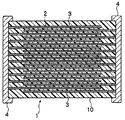
図1は、本発明の積層型セラミックコンデンサの一例を模式的に示す断面図である。本発明の積層型セラミックコンデンサは、図1に示されるように、誘電体層2と内部電極層3とが交互に積層された積層体(以下、積層誘電体素子本体10という。)を有している。積層誘電体素子本体10の両端部には、この積層誘電体素子本体10の内部で交互に配置された内部電極層3と各々導通する一対の外部電極4が形成されている。積層誘電体素子本体10の形状は、通常、直方体状であるが特に制限されない。また、その寸法も特に制限はないが、通常、長辺が0.6〜5.6mm程度、短辺が0.3〜5.0mm程度、高さが0.3〜1.9mm程度である。
(Multilayer ceramic capacitor)
FIG. 1 is a cross-sectional view schematically showing an example of the multilayer ceramic capacitor of the present invention. As shown in FIG. 1, the multilayer ceramic capacitor of the present invention has a multilayer body in which dielectric layers 2 and
誘電体層2は、チタン酸バリウムを含む主成分と、MgO、CaO、BaO、及びSrOから選択される少なくとも1種からなる第1副成分と、Rの酸化物(但し、RはY、Dy、Ho、及びErから選択される少なくとも1種)からなる第2副成分とを少なくとも有する焼結体からなる。 The dielectric layer 2 includes a main component containing barium titanate, a first subcomponent consisting of at least one selected from MgO, CaO, BaO, and SrO, and an oxide of R (where R is Y, Dy , Ho, and Er. The sintered body has at least a second subcomponent consisting of at least one selected from Er, Ho, and Er.
チタン酸バリウム(BaTiO3) に対する上記各副成分の比率は、チタン酸バリウム100モルに対し、第1副成分:0モルを超え0.1モル未満、第2副成分:1モルを超え7モル未満である。 The ratio of each of the above-mentioned subcomponents to barium titanate (BaTiO 3 ) is as follows. Is less than.
本明細書では、チタン酸バリウム及び各副成分を構成する各酸化物を化学量論組成で表しているが、各酸化物の酸化状態は、化学量論組成から外れるものであってもよい。但し、各副成分の上記比率は、各副成分を構成する酸化物に含有される金属量から上記化学量論組成の酸化物に換算して求める。 In this specification, barium titanate and each oxide constituting each subcomponent are represented by a stoichiometric composition, but the oxidation state of each oxide may be out of the stoichiometric composition. However, the said ratio of each subcomponent is calculated | required by converting into the oxide of the said stoichiometric composition from the metal amount contained in the oxide which comprises each subcomponent.
上記各副成分の含有量の限定理由は以下のとおりである。 The reasons for limiting the contents of the subcomponents are as follows.
第1副成分は、MgO、CaO、BaO、及びSrOから選択される少なくとも1種からなるものである。この第1副成分は、容量温度特性を平坦化させる効果を示す。第1副成分の含有量が少なすぎると、この効果が不十分となり、容量温度特性は全般的に悪化する。一方、第1副成分の含有量が本発明の範囲を超えて多くなると、高温側の容量温度特性が再び悪化する傾向がある。なお、第1副成分中における各酸化物の構成比率は任意である。 The first subcomponent is composed of at least one selected from MgO, CaO, BaO, and SrO. This first subcomponent exhibits the effect of flattening the capacity-temperature characteristic. If the content of the first subcomponent is too small, this effect is insufficient, and the capacity-temperature characteristic is generally deteriorated. On the other hand, when the content of the first subcomponent increases beyond the range of the present invention, the capacity-temperature characteristic on the high temperature side tends to deteriorate again. The composition ratio of each oxide in the first subcomponent is arbitrary.
第2副成分は、Rの酸化物(但し、RはY、Dy、Ho、及びErから選択される少なくとも1種)からなるものである。この第2副成分は、キュリー温度を高温側へシフトさせる効果と、容量温度特性を平坦化させる効果とを示す。第2副成分の含有量が少なすぎると、このような効果が不十分となり、容量温度特性が悪くなってしまう。一方、含有量が多すぎると、焼結性が急激に悪化する傾向にある。なお、第2副成分中における各酸化物の構成比率は任意である。 The second subcomponent is composed of an oxide of R (where R is at least one selected from Y, Dy, Ho, and Er). This second subcomponent exhibits the effect of shifting the Curie temperature to the high temperature side and the effect of flattening the capacity-temperature characteristics. When there is too little content of a 2nd subcomponent, such an effect will become inadequate and a capacity | capacitance temperature characteristic will worsen. On the other hand, when there is too much content, it exists in the tendency for sinterability to deteriorate rapidly. The constituent ratio of each oxide in the second subcomponent is arbitrary.
上記の誘電体磁器組成物には、必要に応じて、以下に説明する第3〜6副成分を添加することができる。 If necessary, the above-mentioned dielectric ceramic composition may contain third to sixth subcomponents described below.
第3副成分は、CaZrO3 又はCaO+ZrO2 からなるものであり、キュリー温度を高温側にシフトさせるほか、容量温度特性の平坦化、絶縁抵抗(IR)の向上、破壊電圧の向上、焼成温度を低下させる、などの効果を有する。チタン酸バリウム100モルに対する第3副成分の比率は、0モルを超え5モル未満であることが好ましく、0モルを超え3モル以下であることがより好ましい。第3副成分の添加量が多すぎると、IR寿命が著しく低下し、容量温度特性が悪化する傾向がある。第3副成分におけるCaとZrの比率は特に限定されず、チタン酸バリウムに固溶させない程度に決定すればよいが、Zrに対するCaのモル比(Ca/Zr)は、好ましくは0.5〜1.5、より好ましくは0.8〜1.5、特に好ましくは0.9〜1.1である。 The third subcomponent is made of CaZrO 3 or CaO + ZrO 2. In addition to shifting the Curie temperature to the high temperature side, the capacitance temperature characteristic is flattened, the insulation resistance (IR) is improved, the breakdown voltage is increased, and the firing temperature is increased. It has the effect of reducing. The ratio of the third subcomponent to 100 mol of barium titanate is preferably more than 0 mol and less than 5 mol, more preferably more than 0 mol and 3 mol or less. When there is too much addition amount of a 3rd subcomponent, IR lifetime will fall remarkably and there exists a tendency for a capacity-temperature characteristic to deteriorate. The ratio of Ca and Zr in the third subcomponent is not particularly limited and may be determined so as not to be dissolved in barium titanate. The molar ratio of Ca to Zr (Ca / Zr) is preferably 0.5 to 1.5, more preferably 0.8 to 1.5, particularly preferably 0.9 to 1.1.
第4副成分は、酸化シリコンを主成分とするものであり、この第4副成分は、主として焼結助剤としての利用を図るためのものではあるが、薄層化した際の初期絶縁抵抗の不良率を改善する成分として利用することも可能である。こうした第4副成分としては、MxSiO3(但し、Mは、Ba、Ca、Sr、Li、及びBから選ばれる少なくとも1種の元素)を用いることができる。第4副成分を表す上記の式において、M=Baの場合にはx=1、M=Caの場合にはx=1、M=Srの場合にはx=1、M=Liの場合にはx=2、M=Bの場合にはx=2/3である。 The fourth subcomponent is mainly composed of silicon oxide, and this fourth subcomponent is mainly intended for use as a sintering aid, but the initial insulation resistance when the layer is thinned. It can also be used as a component for improving the defect rate. As the fourth subcomponent, M x SiO 3 (where M is at least one element selected from Ba, Ca, Sr, Li, and B) can be used. In the above formula representing the fourth subcomponent, when M = Ba, x = 1, when M = Ca, x = 1, when M = Sr, x = 1, and when M = Li Where x = 2 and M = B, x = 2/3.
チタン酸バリウム100モルに対する第4副成分(MxSiO3)の比率は、2モル以上10モル以下であることが好ましく、2モル以上6モル以下であることがより好ましい。第4副成分(MxSiO3)の含有量が少なすぎると、容量温度特性を満足できない傾向があり、また絶縁抵抗(IR)が悪化する傾向があり、特に焼結性が著しく悪くなる傾向がある。一方、含有量が多すぎると、絶縁抵抗の寿命特性が不十分となり、誘電率の急激な低下が起こる傾向がある。なお、第4副成分中における各酸化物の構成比率は任意である。 The ratio of the fourth subcomponent (M x SiO 3 ) to 100 mol of barium titanate is preferably 2 mol or more and 10 mol or less, and more preferably 2 mol or more and 6 mol or less. If the content of the fourth subcomponent (M x SiO 3 ) is too small, the capacity-temperature characteristic tends to be unsatisfactory, and the insulation resistance (IR) tends to deteriorate, particularly the sinterability tends to deteriorate remarkably. There is. On the other hand, when the content is too large, the life characteristics of the insulation resistance become insufficient, and the dielectric constant tends to decrease rapidly. The constituent ratio of each oxide in the fourth subcomponent is arbitrary.
第5副成分は、MnO又はCr2O3からなるものであり、焼結を促進する効果と、IRを高くする効果と、IR寿命を向上させる効果とを示す。チタン酸バリウム100モルに対する第5副成分の比率は、0モルを超え≦0.5モル以下であることが好ましく、0.1モル以上0.5モル以下であることがより好ましい。第5副成分の含有量が多すぎると、容量温度特性に悪影響を与え、IR寿命を悪化させるおそれがある。なお、第5副成分中における各酸化物の構成比率は任意である。 The fifth subcomponent is made of MnO or Cr 2 O 3 and exhibits an effect of promoting sintering, an effect of increasing IR, and an effect of improving IR life. The ratio of the fifth subcomponent to 100 mol of barium titanate is preferably more than 0 mol and ≦ 0.5 mol or less, and more preferably 0.1 mol or more and 0.5 mol or less. When there is too much content of a 5th subcomponent, there exists a possibility of having a bad influence on a capacity temperature characteristic and making IR life worse. The constituent ratio of each oxide in the fifth subcomponent is arbitrary.
第6副成分は、V2O5、MoO3、及びWO3 から選択される少なくとも1種からなるものであり、キュリー温度以上での容量温度特性を平坦化する効果と、IR寿命を向上させる効果とを示す。チタン酸バリウム100モルに対する第6副成分の比率は、0.01モル以上0.5モル以下であることが好ましく、0.01モル以上0.2モル以下であることがより好ましい。第6副成分の含有量が少なすぎると、上述した効果が不十分となる傾向がある。一方、含有量が多すぎると、IRが著しく低下する。なお、第6副成分中における各酸化物の構成比率は任意である。 The sixth subcomponent is composed of at least one selected from V 2 O 5 , MoO 3 , and WO 3 and improves the effect of flattening the capacity-temperature characteristics above the Curie temperature and the IR lifetime. Show the effect. The ratio of the sixth subcomponent with respect to 100 mol of barium titanate is preferably 0.01 mol or more and 0.5 mol or less, and more preferably 0.01 mol or more and 0.2 mol or less. When there is too little content of a 6th subcomponent, there exists a tendency for the effect mentioned above to become inadequate. On the other hand, when there is too much content, IR will fall remarkably. The constituent ratio of each oxide in the sixth subcomponent is arbitrary.
誘電体磁器組成物中には、以上説明した主成分及び第1〜6副成分のほかに、Al2O3を含む第7副成分がさらに添加してあってもよい。Al2O3は容量温度特性にあまり影響を与えず、焼結性、IR及びIR寿命を改善する効果を示す。但し、Al2O3の含有量が多すぎると焼結性が悪化してIRが低くなる。このため、第7副成分の比率は、チタン酸バリウム100モルに対して1モル以下であることが好ましく、誘電体磁器組成物全体の1モル以下であることがより好ましい。 In addition to the main component and the first to sixth subcomponents described above, a seventh subcomponent containing Al 2 O 3 may be further added to the dielectric ceramic composition. Al 2 O 3 does not significantly affect the capacity-temperature characteristics and shows the effect of improving the sinterability, IR, and IR life. However, IR is lower sinterability and the content of Al 2 O 3 is too large to deteriorate. For this reason, the ratio of the seventh subcomponent is preferably 1 mol or less with respect to 100 mol of barium titanate, and more preferably 1 mol or less of the entire dielectric ceramic composition.
上述した組成を有する誘電体磁器組成物のキュリー温度(強誘電体から常誘電体への相転移温度)は、誘電体磁器組成物の組成を選択することにより変更することができるが、X8R特性を満足するためには、好ましくは120℃以上、より好ましくは123℃以上とする。キュリー温度は、DSC(示差走査熱量測定)等によって測定することができる。なお、Sr、Zr及びSnの少なくとも1種が、ペロブスカイト構造を構成するチタン酸バリウム中のBa又はTiを置換している場合には、キュリー温度が低温側にシフトするため、125℃以上での容量温度特性が悪くなる。このため、これらの元素を含むチタン酸バリウム系複合酸化物[例えば(Ba,Sr)TiO3] は主成分として用いないことが好ましい。但し、Sr、Zr及びSnの少なくとも1種が不純物として含有されるレベル(例えば誘電体磁器組成物全体の0.1モル%程度以下)であれば、特に問題はない。 The Curie temperature (phase transition temperature from ferroelectric to paraelectric) of the dielectric ceramic composition having the above composition can be changed by selecting the composition of the dielectric ceramic composition. Is preferably 120 ° C. or higher, more preferably 123 ° C. or higher. The Curie temperature can be measured by DSC (differential scanning calorimetry) or the like. In addition, when at least one of Sr, Zr, and Sn substitutes Ba or Ti in barium titanate constituting the perovskite structure, the Curie temperature shifts to the low temperature side, so that the temperature is 125 ° C. or higher. Capacitance-temperature characteristics deteriorate. For this reason, it is preferable not to use the barium titanate complex oxide [for example (Ba, Sr) TiO 3 ] containing these elements as a main component. However, there is no particular problem as long as at least one of Sr, Zr, and Sn is contained as an impurity (for example, about 0.1 mol% or less of the entire dielectric ceramic composition).
次に、誘電体層2を構成する結晶粒子(以下、「誘電体粒子」という。)について説明する。 Next, crystal particles constituting the dielectric layer 2 (hereinafter referred to as “dielectric particles”) will be described.
誘電体粒子は、上述した誘電体層2を構成するものであり、本発明においては、その誘電体粒子の平均粒径が0.25μm以上0.42μm以下であることに特徴がある。誘電体粒子の平均粒径がこの範囲内にあることにより、製造された積層型セラミックコンデンサは、その容量温度特性がEIA規格のX8R特性(−55〜150℃、ΔC/C=±15%以内)を満足し、且つ容量の経時変化が小さいという効果を奏する。 The dielectric particles constitute the dielectric layer 2 described above, and the present invention is characterized in that the average particle diameter of the dielectric particles is not less than 0.25 μm and not more than 0.42 μm. Due to the average particle size of the dielectric particles being within this range, the produced multilayer ceramic capacitor has an EIA standard X8R characteristic (−55 to 150 ° C., ΔC / C = within ± 15%). ) And the change in capacity over time is small.
誘電体粒子の平均粒径が0.25μm未満では、誘電体層2を薄層化したとき(例えば層間での厚さを3.5μmより小さくしたとき)や、積層誘電体素子本体10を多層化したとき(例えば誘電体層2の層数を100以上にしたとき)に、X8R特性を満たさなくなることがある。また、誘電体粒子の平均粒径が0.42μmを超えると、容量の経時変化が大きくなって安定したコンデンサとして使用することができなくなることがある。
When the average particle diameter of the dielectric particles is less than 0.25 μm, the dielectric layer 2 is thinned (for example, when the thickness between the layers is smaller than 3.5 μm), or the laminated
誘電体粒子の平均粒径は0.25μm以上0.34μm以下であることがより好ましい。誘電体粒子の平均粒径がこの範囲内にあることにより、製造された積層型セラミックコンデンサは、その容量温度特性がEIA規格のX8R特性を満足すると共に容量の経時変化が小さいという上記の特性に加え、Tcバイアス特性に優れるという効果を奏する。特に、この態様においては、誘電体粒子の平均粒径が0.34μm以下であることにより、Tcバイアス特性の優れた積層型セラミックコンデンサを得ることができる。 The average particle size of the dielectric particles is more preferably 0.25 μm or more and 0.34 μm or less. Due to the average particle size of the dielectric particles being within this range, the manufactured multilayer ceramic capacitor has the above characteristics that its capacitance-temperature characteristic satisfies the X8R characteristic of the EIA standard and its change with time is small. In addition, the Tc bias characteristic is excellent. In particular, in this embodiment, when the average particle diameter of the dielectric particles is 0.34 μm or less, a multilayer ceramic capacitor having excellent Tc bias characteristics can be obtained.
また、本発明においては、その誘電体粒子の最大粒径(D100)と平均粒径(D50)との差(D100−D50値)が0.07μm以下であることが好ましい。誘電体粒子がD100−D50値で0.07μm以下であることにより、製造された積層型セラミックコンデンサは、その容量温度特性がEIA規格のX8R特性を満足すると共に容量の経時変化が小さいという上記の特性に加え、Tcバイアス特性に優れるという効果を奏する。 In the present invention, the difference (D100-D50 value) between the maximum particle size (D100) and the average particle size (D50) of the dielectric particles is preferably 0.07 μm or less. When the dielectric particles have a D100-D50 value of 0.07 μm or less, the produced multilayer ceramic capacitor satisfies the EIA standard X8R characteristic and has a small change with time. In addition to the characteristics, the Tc bias characteristics are excellent.
なお、本発明において、誘電体粒子の平均粒径は、コード法により決定される。また、D100−D50値は、誘電体粒子の最大粒径(D100)と平均粒径(D50)との差を表しているが、その最大粒径と平均粒径とは、誘電体層2を構成する誘電体粒子の粒度分布を予め求め、その粒度分布から得られた最大粒径と平均粒径とを用いて算出される。D100−D50値が小さいということは、誘電体層2を構成する誘電体粒子の大きさのバラツキが少ないことを意味している。 In the present invention, the average particle diameter of the dielectric particles is determined by a code method. The D100-D50 value represents the difference between the maximum particle size (D100) and the average particle size (D50) of the dielectric particles. The particle size distribution of the constituent dielectric particles is obtained in advance, and is calculated using the maximum particle size and the average particle size obtained from the particle size distribution. The small D100-D50 value means that there is little variation in the size of the dielectric particles constituting the dielectric layer 2.
また、容量温度特性がEIA規格のX8R特性を満足するとは、製造された積層型セラミックコンデンサが、80℃以上、特に125〜150℃の環境下で使用される機器用電子部品として好ましく用いることができることを示すものである。そして、このような温度範囲において、容量の温度特性がEIAJ規格のR特性を満足し、さらにX8R特性(−55〜150℃、ΔC/C=±15%以内)も満足することを意味している。また、JIS規格のB特性[−25〜85℃で容量変化率±10%以内(基準温度20℃)]、EIA規格のX7R特性(−55〜125℃、ΔC=±15%以内)も同時に満足することが可能である。
Further, when the capacitance-temperature characteristic satisfies the X8R characteristic of the EIA standard, the manufactured multilayer ceramic capacitor is preferably used as an electronic component for equipment used in an environment of 80 ° C. or higher, particularly 125 to 150 ° C. It shows what can be done. And in such a temperature range, it means that the temperature characteristic of the capacity satisfies the R characteristic of the EIAJ standard and further satisfies the X8R characteristic (−55 to 150 ° C., within ΔC / C = ± 15%). Yes. In addition, the B characteristic of JIS standard [capacitance change rate within −10% at −25 to 85 ° C. (
また、容量の経時変化に優れるとは、製造された積層型セラミックコンデンサを例えば85℃の温度環境下で例えば7V/μmの直流電圧を印加した場合等において、1000時間後における容量の変化率が−10%以内であることを意味している。 In addition, it is said that the capacity change rate after 1000 hours is excellent when the manufactured multilayer ceramic capacitor is applied with a DC voltage of, for example, 7 V / μm in a temperature environment of 85 ° C. It means within -10%.
また、Tcバイアス特性に優れるとは、製造された積層型セラミックコンデンサに、通常0.02V/μm以上、特に0.2V/μm以上、さらには0.5V/μm以上、一般に5V/μm程度以下の交流電界と、これに重畳して5V/μm以下の直流電界とが加えられた場合においても、容量の温度特性が安定であり、Tcバイアス時の容量変化率が例えば−40%以内であることを意味している。 The excellent Tc bias characteristic means that the manufactured multilayer ceramic capacitor is usually 0.02 V / μm or more, particularly 0.2 V / μm or more, more preferably 0.5 V / μm or more, and generally about 5 V / μm or less. Even when an AC electric field and a DC electric field of 5 V / μm or less are applied in a superimposed manner, the temperature characteristic of the capacitance is stable, and the rate of change in capacitance at Tc bias is, for example, within −40%. It means that.
誘電体層2の積層数や厚さ等の諸条件は、目的や用途に応じ適宜決定すればよいが、誘電体層2の厚さとしては、通常30μm以下であり、小型大容量化の観点からは、誘電体層2の厚さを10μm以下とすることが好ましい。このように薄層化した誘電体層2を有する積層型セラミックコンデンサは、小型化大容量化を実現できると共に、その誘電体層2を構成する誘電体粒子の平均粒径等が特定されることにより、容量温度特性等の改善に有効である。なお、誘電体層2の厚さの下限は特に制限されないが、強いて挙げれば0.5μm程度である。また、誘電体層2の積層数は、通常、50〜1000程度である。 Various conditions such as the number and thickness of the dielectric layers 2 may be appropriately determined according to the purpose and application. However, the thickness of the dielectric layer 2 is usually 30 μm or less, and from the viewpoint of reducing the size and increasing the capacity. Therefore, the thickness of the dielectric layer 2 is preferably 10 μm or less. The multilayer ceramic capacitor having the thinned dielectric layer 2 can realize a reduction in size and an increase in capacity, and the average particle diameter of the dielectric particles constituting the dielectric layer 2 can be specified. Therefore, it is effective for improving the capacity-temperature characteristics. In addition, the lower limit of the thickness of the dielectric layer 2 is not particularly limited, but it is about 0.5 μm if it is given. Further, the number of laminated dielectric layers 2 is usually about 50 to 1000.
内部電極層3は、以上説明した誘電体層2と交互に設けられ、各端面が積層誘電体素子本体10の対向する2つの端部の表面に交互に露出するように積層されている。また、一対の外部電極4は、積層誘電体素子本体10の両端部に形成され、交互に配置されたニッケル内部電極層3の露出端面に接続されて、積層型セラミックコンデンサを構成している。
The
内部電極層3は、実質的に電極として作用する卑金属の導電材から構成される。具体的には、Ni又はNi合金が好ましい。Ni合金としては、Mn、Cr、Co、Al、W等の1種又は2種以上と、Niとの合金が好ましく、合金中のNi含有量が95重量%以上であることが好ましい。また、Ni又はNi合金中には、P、C、Nb、Fe、Cl、B、Li、Na、K、F、S等の各種微量成分が0.1重量%以下含有されていてもよい。内部電極層3の積層数や厚さ等の諸条件は、目的や用途に応じ適宜決定すればよいが、厚さとしては、通常0.1μm〜3.0μm程度が好ましく、0.2μm〜2.0μmがより好ましい。
The
外部電極4は、積層誘電体素子本体10の内部で交互に配置された内部電極層3と各々導通する電極であり、積層誘電体素子本体10の両端部に一対形成されている。外部電極4としては、通常、Ni、Pd、Ag、Au、Cu、Pt、Rh、Ru、Ir等の少なくとも1種又はそれらの合金を用いることができる。通常は、Cu、Cu合金、Ni又はNi合金等や、Ag、Ag−Pd合金、In−Ga合金等が使用される。外部電極4の厚さは用途等に応じて適宜決定されればよいが、通常、10〜200μm程度であることが好ましい。
The external electrodes 4 are electrodes that are electrically connected to the
(積層型セラミックコンデンサの製造方法)
本発明の積層型セラミックコンデンサは、従来の積層型セラミックコンデンサと同様に、ペーストを用いた通常の印刷法やシート法によりグリーンチップを作製し、これを焼成した後、外部電極を印刷又は転写して焼成することにより製造される。以下、製造方法について具体的に説明する。
(Manufacturing method of multilayer ceramic capacitor)
In the multilayer ceramic capacitor of the present invention, as in the conventional multilayer ceramic capacitor, a green chip is produced by a normal printing method or sheet method using a paste, and this is fired, and then an external electrode is printed or transferred. It is manufactured by baking. Hereinafter, the manufacturing method will be specifically described.
誘電体層用ペーストは、誘電体原料と有機ビヒクルとを混練した有機系の塗料であってもよく、水系の塗料であってもよい。 The dielectric layer paste may be an organic paint obtained by kneading a dielectric material and an organic vehicle, or may be a water-based paint.
誘電体原料には、上記した酸化物やその混合物、複合酸化物を用いることができるが、その他、焼成により上記した酸化物や複合酸化物となる各種化合物、例えば炭酸塩、シュウ酸塩、硝酸塩、水酸化物、有機金属化合物等から適宜選択し、混合して用いることができる。誘電体原料中の各化合物の含有量は、焼成後に上記した誘電体磁器組成物の組成となるように決定すればよい。この誘電体原料は、通常、平均粒径0.1〜3.0μm程度の粉末が用いられる。 As the dielectric material, the above-described oxide, a mixture thereof, or a composite oxide can be used. In addition, various compounds that become the above-described oxide or composite oxide upon firing, such as carbonates, oxalates, and nitrates. , Hydroxides, organometallic compounds and the like can be selected as appropriate and used in combination. What is necessary is just to determine content of each compound in a dielectric raw material so that it may become a composition of the above-mentioned dielectric ceramic composition after baking. As the dielectric material, a powder having an average particle size of about 0.1 to 3.0 μm is usually used.
有機ビヒクルとは、バインダを有機溶剤中に溶解したものである。有機ビヒクルに用いるバインダは特に限定されず、エチルセルロース、ポリビニルブチラール等の通常の各種バインダから適宜選択すればよい。また、用いる有機溶剤も特に限定されず、印刷法やシート法等、利用する方法に応じて、テルピネオール、ブチルカルビトール、アセトン、トルエン等の各種有機溶剤から適宜選択すればよい。 An organic vehicle is obtained by dissolving a binder in an organic solvent. The binder used for the organic vehicle is not particularly limited, and may be appropriately selected from usual various binders such as ethyl cellulose and polyvinyl butyral. Moreover, the organic solvent to be used is not particularly limited, and may be appropriately selected from various organic solvents such as terpineol, butyl carbitol, acetone, toluene, and the like, depending on a method to be used such as a printing method or a sheet method.
また、誘電体層用ペーストを水系の塗料とする場合には、水溶性のバインダや分散剤等を水に溶解させた水系ビヒクルと、誘電体原料とを混練すればよい。水系ビヒクルに用いる水溶性バインダは特に限定されず、例えばポリビニルアルコール、セルロース、水溶性アクリル樹脂等を用いればよい。 In addition, when the dielectric layer paste is used as a water-based paint, a water-based vehicle in which a water-soluble binder, a dispersant or the like is dissolved in water and a dielectric material may be kneaded. The water-soluble binder used for the water-based vehicle is not particularly limited, and for example, polyvinyl alcohol, cellulose, water-soluble acrylic resin, etc. may be used.
内部電極層用ペーストは、上記した各種誘電性金属や合金からなる導電材、あるいは焼成後に上記した導電材となる各種酸化物、有機金属化合物、レジネート等と、上記した有機ビヒクルとを混練して調製する。外部電極用ペーストは、上記した内部電極層用ペーストと同様にして調製すればよい。 The internal electrode layer paste is prepared by kneading the above-mentioned organic vehicle with various conductive metals made of various dielectric metals and alloys, or various oxides, organometallic compounds, resinates, etc. that become the above-mentioned conductive materials after firing. Prepare. The external electrode paste may be prepared in the same manner as the internal electrode layer paste described above.
上記した各ペースト中の有機ビヒクルの含有量に特に制限はなく、通常の含有量、例えば、バインダは1〜5重量%程度、溶剤は10〜50重量%程度とすればよい。また、各ペースト中には、必要に応じて各種分散剤、可塑剤、誘電体、絶縁体等から選択される添加物が含有されていてもよい。これらの総含有量は、10重量%以下とすることが好ましい。 There is no restriction | limiting in particular in content of the organic vehicle in each above-mentioned paste, For example, what is necessary is just about 1-5 weight% of binders, for example, about 10-50 weight% of binders. Each paste may contain additives selected from various dispersants, plasticizers, dielectrics, insulators, and the like as necessary. The total content of these is preferably 10% by weight or less.
印刷法を用いる場合、誘電体層用ペースト及び内部電極層用ペーストを、ポリエチレンテレフタレート(PET)フィルム等の基板上に積層印刷し、所定形状に切断した後、基板から剥離してグリーンチップとする。また、シート法を用いる場合、誘電体層用ペーストを用いてグリーンシートを形成し、この上に内部電極層用ペーストを印刷した後、これらを積層してグリーンチップとする。 When using the printing method, the dielectric layer paste and the internal electrode layer paste are laminated and printed on a substrate such as a polyethylene terephthalate (PET) film, cut into a predetermined shape, and then peeled off from the substrate to obtain a green chip. . When the sheet method is used, a dielectric layer paste is used to form a green sheet, the internal electrode layer paste is printed thereon, and these are stacked to form a green chip.
焼成前に、グリーンチップに脱バインダ処理を施す。脱バインダ処理は、通常の条件で行えばよいが、内部電極層の導電材にNiやNi合金等の卑金属を用いる場合には、空気雰囲気において、昇温速度を好ましくは5〜300℃/時間、より好ましくは10〜100℃/時間、保持温度を好ましくは180〜400℃、より好ましくは200〜300℃、温度保持時間を好ましくは0.5〜24時間、より好ましくは5〜20時間とする。 Before firing, the green chip is subjected to binder removal processing. The binder removal process may be performed under normal conditions. However, when a base metal such as Ni or Ni alloy is used as the conductive material of the internal electrode layer, the heating rate is preferably 5 to 300 ° C./hour in an air atmosphere. More preferably, the temperature is 10 to 100 ° C./hour, the holding temperature is preferably 180 to 400 ° C., more preferably 200 to 300 ° C., and the temperature holding time is preferably 0.5 to 24 hours, more preferably 5 to 20 hours. To do.
グリーンチップ焼成時の雰囲気は、内部電極層用ペースト中の導電材の種類に応じて適宜決定されればよいが、導電材としてNiやNi合金等の卑金属を用いる場合、焼成雰囲気中の酸素分圧は、10−8〜10−12気圧とすることが好ましい。酸素分圧が前記範囲未満であると、内部電極層の導電材が異常焼結を起こし、途切れてしまうことがある。また、酸素分圧が前記範囲を超えると、内部電極層が酸化する傾向にある。 The atmosphere at the time of green chip firing may be appropriately determined according to the type of conductive material in the internal electrode layer paste, but when a base metal such as Ni or Ni alloy is used as the conductive material, the oxygen content in the firing atmosphere The pressure is preferably 10 −8 to 10 −12 atm. When the oxygen partial pressure is less than the above range, the conductive material of the internal electrode layer may be abnormally sintered and may be interrupted. Further, when the oxygen partial pressure exceeds the above range, the internal electrode layer tends to be oxidized.
また、焼成時の保持温度は、好ましくは1100〜1400℃、より好ましくは1200〜1360℃、さらに好ましくは1200〜1340℃である。保持温度が前記範囲未満であると緻密化が不十分となり、前記範囲を超えると、内部電極層の異常焼結による電極の途切れや、内部電極層構成材料の拡散による容量温度特性の悪化、誘電体磁器組成物の還元が生じやすくなる。 Moreover, the holding temperature at the time of baking becomes like this. Preferably it is 1100-1400 degreeC, More preferably, it is 1200-1360 degreeC, More preferably, it is 1200-1340 degreeC. If the holding temperature is lower than the above range, the densification becomes insufficient. If the holding temperature is higher than the above range, the electrode temperature is interrupted due to abnormal sintering of the internal electrode layer, the capacity temperature characteristic deteriorates due to diffusion of the constituent material of the internal electrode layer, and the dielectric Reduction of the body porcelain composition is likely to occur.
これ以外の焼成条件としては、昇温速度を好ましくは50〜500℃/時間、より好ましくは200〜300℃/時間、温度保持時間を好ましくは0.5〜8時間、より好ましくは1〜3時間、冷却速度を好ましくは50〜500℃/時間、より好ましくは200〜300℃/時間とする。また、焼成雰囲気は還元性雰囲気とすることが好ましく、雰囲気ガスとしては、例えばN2 とH2 との混合ガスを加湿して用いることが好ましい。 As other firing conditions, the rate of temperature rise is preferably 50 to 500 ° C./hour, more preferably 200 to 300 ° C./hour, and the temperature holding time is preferably 0.5 to 8 hours, more preferably 1 to 3 hours. The time and cooling rate are preferably 50 to 500 ° C./hour, more preferably 200 to 300 ° C./hour. Further, the firing atmosphere is preferably a reducing atmosphere, and as the atmosphere gas, for example, a mixed gas of N 2 and H 2 is preferably used after being humidified.
還元性雰囲気中で焼成した場合、積層誘電体素子本体にはアニールを施すことが好ましい。アニールは、誘電体層を再酸化するための処理であり、これによりIR寿命を著しく長くすることができるので、信頼性が向上する。 When firing in a reducing atmosphere, it is preferable to anneal the multilayer dielectric element body. Annealing is a process for re-oxidizing the dielectric layer, and this can significantly increase the IR lifetime, thereby improving the reliability.
アニール雰囲気中の酸素分圧は、10−10気圧以上、特に10−7〜10−6気圧とすることが好ましい。酸素分圧が前記範囲未満であると誘電体層の再酸化が困難であり、前記範囲を超えると内部電極層が酸化する傾向にある。 The oxygen partial pressure in the annealing atmosphere is preferably 10 −10 atm or more, particularly 10 −7 to 10 −6 atm. When the oxygen partial pressure is less than the above range, it is difficult to reoxidize the dielectric layer, and when it exceeds the above range, the internal electrode layer tends to be oxidized.
アニールの際の保持温度は、1100℃以下、特に500〜1100℃とすることが好ましい。保持温度が前記範囲未満であると誘電体層の酸化が不十分となるので、IRが低く、また、IR寿命が短くなりやすい。一方、保持温度が前記範囲を超えると、内部電極層が酸化して容量が低下するだけでなく、内部電極層が誘電体素地と反応してしまい、容量温度特性の悪化、IRの低下、IR寿命の低下が生じやすくなる。なお、アニールは昇温過程及び降温過程だけから構成してもよい。すなわち、温度保持時間を零としてもよい。この場合、保持温度は最高温度と同義である。 The holding temperature at the time of annealing is preferably 1100 ° C. or less, particularly 500 to 1100 ° C. When the holding temperature is lower than the above range, the dielectric layer is not sufficiently oxidized, so that the IR is low and the IR life tends to be short. On the other hand, if the holding temperature exceeds the above range, not only the internal electrode layer is oxidized and the capacity is lowered, but the internal electrode layer reacts with the dielectric substrate, the capacity temperature characteristic is deteriorated, the IR is lowered, the IR Life is likely to decrease. In addition, you may comprise annealing only from a temperature rising process and a temperature falling process. That is, the temperature holding time may be zero. In this case, the holding temperature is synonymous with the maximum temperature.
これ以外のアニール条件としては、温度保持時間を好ましくは0〜20時間、より好ましくは6〜10時間、冷却速度を好ましくは50〜500℃/時間、より好ましくは100〜300℃/時間とする。また、アニールの雰囲気ガスとしては、例えば、加湿したN2 ガス等を用いることが好ましい。 As other annealing conditions, the temperature holding time is preferably 0 to 20 hours, more preferably 6 to 10 hours, and the cooling rate is preferably 50 to 500 ° C./hour, more preferably 100 to 300 ° C./hour. . Further, as the atmosphere gas for annealing, for example, humidified N 2 gas or the like is preferably used.
上記した脱バインダ処理、焼成及びアニールにおいて、N2 ガスや混合ガス等を加湿するには、例えばウェッター等を使用すればよい。この場合、水温は5〜75℃程度が好ましい。 In the above-described binder removal processing, firing and annealing, for example, a wetter or the like may be used to wet the N 2 gas, mixed gas, or the like. In this case, the water temperature is preferably about 5 to 75 ° C.
脱バインダ処理、焼成及びアニールは、連続して行っても、独立に行ってもよい。これらを連続して行う場合、脱バインダ処理後、冷却せずに雰囲気を変更し、続いて焼成の際の保持温度まで昇温して焼成を行い、次いで冷却し、アニールの保持温度に達したときに雰囲気を変更してアニールを行うことが好ましい。一方、これらを独立して行う場合、焼成に際しては、脱バインダ処理時の保持温度までN2 ガスあるいは加湿したN2 ガス雰囲気下で昇温した後、雰囲気を変更してさらに昇温を続けることが好ましく、アニール時の保持温度まで冷却した後は、再びN2 ガスあるいは加湿したN2 ガス雰囲気に変更して冷却を続けることが好ましい。また、アニールに際しては、N2 ガス雰囲気下で保持温度まで昇温した後、雰囲気を変更してもよく、アニールの全過程を加湿したN2 ガス雰囲気としてもよい。 The binder removal treatment, firing and annealing may be performed continuously or independently. When these are performed continuously, after removing the binder, the atmosphere is changed without cooling, and then the firing is performed by raising the temperature to the holding temperature during firing, followed by cooling to reach the annealing holding temperature. It is sometimes preferable to perform annealing by changing the atmosphere. On the other hand, when performing these independently, after firing, the temperature is raised in the N 2 gas or humidified N 2 gas atmosphere to the holding temperature at the time of the binder removal process, and then the temperature is further changed by continuing the temperature rise. Preferably, after cooling to the holding temperature at the time of annealing, it is preferable to change to the N 2 gas or humidified N 2 gas atmosphere again and continue cooling. In annealing, the temperature may be changed to a holding temperature in an N 2 gas atmosphere, and then the atmosphere may be changed, or the entire annealing process may be a humidified N 2 gas atmosphere.
上記のようにして得られた積層誘電体素子本体に、例えばバレル研磨やサンドブラスト等により端面研磨を施し、外部電極用ペーストを印刷又は転写して焼成し、外部電極4を形成する。外部電極用ペーストの焼成条件は、例えば、加湿したN2 とH2 との混合ガス中で600〜800℃にて10分間〜1時間程度とすることが好ましい。そして、必要に応じ、外部電極4表面に、めっき等により被覆層を形成する。このようにして製造された本発明の積層型セラミックコンデンサは、ハンダ付等によりプリント基板上等に実装され、各種電子機器等に使用される。 The laminated dielectric element main body obtained as described above is subjected to end face polishing, for example, by barrel polishing or sand blasting, and the external electrode paste is printed or transferred and baked to form the external electrode 4. The firing conditions of the external electrode paste are preferably, for example, about 10 minutes to 1 hour at 600 to 800 ° C. in a humidified mixed gas of N 2 and H 2 . Then, if necessary, a coating layer is formed on the surface of the external electrode 4 by plating or the like. The multilayer ceramic capacitor of the present invention thus manufactured is mounted on a printed circuit board or the like by soldering or the like and used for various electronic devices.
以上本発明の積層型セラミックコンデンサ及びその製造方法について説明してきたが、本発明はこうした実施形態に何等限定されるものではなく、本発明の要旨を逸脱しない範囲内において種々なる態様で実施し得ることは勿論である。 The multilayer ceramic capacitor and the method for manufacturing the same according to the present invention have been described above. However, the present invention is not limited to these embodiments, and can be implemented in various modes without departing from the scope of the present invention. Of course.
以下の実験例により本発明を詳細に説明する。但し、本発明は、以下の記載内容に限定されるものではない。 The following experimental examples illustrate the invention in detail. However, the present invention is not limited to the following description.
(実験1)
先ず、誘電体材料を作製するための出発原料として、それぞれの平均粒径が0.1〜1μmに含まれる主成分原料(BaTiO3) 及び第1〜第6副成分原料を用意した。特にBaTiO3 については、原料粉末の平均粒径が約0.1〜0.33μmであり且つN2 吸着法を用いて測定された比表面積が3〜8.5の範囲のもの、具体的には固相法で合成した比表面積が3.0、4.1、4.4、5.0、5.4、6.0、7.0、8.5の8種類のBaTiO3 粉末を使用した。なお、比表面積が前記範囲となるBaTiO3 は、固相法に限らず、一般的な液相合成によっても得ることができる。
(Experiment 1)
First, as starting materials for producing a dielectric material, main component materials (BaTiO 3 ) and first to sixth subcomponent materials each having an average particle diameter of 0.1 to 1 μm were prepared. In particular, for BaTiO 3 , the raw material powder has an average particle size of about 0.1 to 0.33 μm and a specific surface area measured using the N 2 adsorption method of 3 to 8.5, specifically Uses 8 types of BaTiO 3 powders with specific surface areas of 3.0, 4.1, 4.4, 5.0, 5.4, 6.0, 7.0, 8.5 synthesized by solid phase method did. Note that BaTiO 3 having a specific surface area in the above range can be obtained not only by the solid phase method but also by general liquid phase synthesis.
第1副成分の出発原料としてはMgCO3 を用い、第2副成分の出発原料としてはY2O3を用いた。また、第3副成分の出発原料としてはCaZrO3 を用い、第4副成分の出発原料としては(BaO0.6,Ca0.4)SiO3 を用いた。そして、第5副成分の出発原料としてはMnCO3 を用い、第6副成分の出発原料としてはV2O5を用いた。なお、第3副成分の出発原料であるCaZrO3 は、CaCO3 及びZrO2 をボールミルにより16時間湿式混合し、乾燥後、1150℃で空気中で焼成し、さらに、ボールミルにより24時間湿式粉砕することにより製造した。また、第4副成分の出発原料である(BaO0.6,Ca0.4)SiO3 は、BaCO3 、CaCO3 及びSiO2 をボールミルにより16時間湿式混合し、乾燥後、1150℃で空気中で焼成し、さらに、ボールミルにより100時間湿式粉砕することにより製造した。 MgCO 3 was used as the starting material for the first subcomponent, and Y 2 O 3 was used as the starting material for the second subcomponent. Further, CaZrO 3 was used as the starting material for the third subcomponent, and (BaO 0.6 , Ca 0.4 ) SiO 3 was used as the starting material for the fourth subcomponent. Then, MnCO 3 was used as the starting material for the fifth subcomponent, and V 2 O 5 was used as the starting material for the sixth subcomponent. In addition, CaZrO 3 as a starting material of the third subcomponent is wet-mixed with CaCO 3 and ZrO 2 by a ball mill for 16 hours, dried, fired in air at 1150 ° C., and further wet-ground by a ball mill for 24 hours. It was manufactured by. In addition, (BaO 0.6 , Ca 0.4 ) SiO 3 which is a starting material of the fourth subcomponent is wet-mixed with BaCO 3 , CaCO 3 and SiO 2 for 16 hours by a ball mill, dried, and air at 1150 ° C. It was manufactured by firing in a ball mill and wet milling with a ball mill for 100 hours.
これらの原料を、焼成後の組成が、主成分であるBaTiO3 100モルに対して、MgCO3 が0.07モル、Y2O3が4.0モル、CaZrO3 が2.00モル、(BaO0.6,Ca0.4)SiO3 が3.0モル、MnCO3 が0.3モル、V2O5が0.06モルとなるように秤量し、ボールミルにより16時間湿式混合してから乾燥させて、誘電体原料とした。 These raw materials, the composition after firing, with respect to BaTiO 3 100 moles of the main component, MgCO 3 0.07 mol, Y 2 O 3 is 4.0 mol, CaZrO 3 2.00 moles ( BaO 0.6 , Ca 0.4 ) SiO 3 is 3.0 mol, MnCO 3 is 0.3 mol, V 2 O 5 is 0.06 mol, and wet-mixed by a ball mill for 16 hours. And dried to obtain a dielectric material.
このようにして得られた乾燥後の誘電体原料100重量部と、アクリル樹脂4.8重量部と、塩化メチレン40重量部と、酢酸エチル20重量部と、ミネラルスピリット6重量部と、アセトン4重量部とをボールミルで混合してペースト化し、誘電体層用ペーストを得た。 100 parts by weight of the dielectric material thus obtained after drying, 4.8 parts by weight of acrylic resin, 40 parts by weight of methylene chloride, 20 parts by weight of ethyl acetate, 6 parts by weight of mineral spirit, and acetone 4 Part by weight was mixed with a ball mill to form a paste, and a dielectric layer paste was obtained.
次いで、平均粒径0.4μmのNi粒子100重量部と、有機ビヒクル(エチルセルロース8重量部をブチルカルビトール92重量部に溶解したもの)40重量部と、ブチルカルビトール10重量部とを3本ロールにより混練してペースト化し、内部電極層用ペーストを得た。 Next, 100 parts by weight of Ni particles having an average particle diameter of 0.4 μm, 40 parts by weight of an organic vehicle (8 parts by weight of ethyl cellulose dissolved in 92 parts by weight of butyl carbitol), and 10 parts by weight of butyl carbitol The paste was kneaded with a roll to obtain an internal electrode layer paste.
次いで、平均粒径0.5μmのCu粒子100重量部と、有機ビヒクル(エチルセルロース樹脂8重量部をブチルカルビトール92重量部に溶解したもの)35重量部及びブチルカルビトール7重量部とを混練してペースト化し、外部電極用ペーストを得た。 Next, 100 parts by weight of Cu particles having an average particle size of 0.5 μm, 35 parts by weight of an organic vehicle (8 parts by weight of ethyl cellulose resin dissolved in 92 parts by weight of butyl carbitol) and 7 parts by weight of butyl carbitol were kneaded. To obtain a paste for an external electrode.
次いで、上記誘電体層用ペーストを用いてPETフィルム上に、厚さ4.5μmのグリーンシートを形成し、この上に内部電極層用ペーストを印刷したのち、PETフィルムからグリーンシートを剥離した。次いで、これらのグリーンシートと保護用グリーンシート(内部電極層用ペーストを印刷しないもの)とを積層、圧着して、グリーンチップを得た。内部電極を有するシートの積層数は4層とした。 Next, a 4.5 μm-thick green sheet was formed on the PET film using the dielectric layer paste, and the internal electrode layer paste was printed thereon, and then the green sheet was peeled from the PET film. Next, these green sheets and protective green sheets (not printed with internal electrode layer paste) were laminated and pressure-bonded to obtain green chips. The number of sheets having internal electrodes was four.
次いで、グリーンチップを所定サイズに切断し、脱バインダ処理、焼成及びアニールを行って、積層セラミック焼成体を得た。脱バインダ処理は、昇温時間15℃/時間、保持温度280℃、保持時間8時間、空気雰囲気の条件で行った。また、焼成は、昇温速度200℃/時間、保持温度1270〜1320℃、保持時間2時間、冷却速度300℃/時間、加湿したN2 +H2 混合ガス雰囲気(酸素分圧は10−11気圧)の条件で行った。アニールは、保持温度900℃、温度保持時間9時間、冷却速度300℃/時間、加湿したN2 ガス雰囲気(酸素分圧は10−7気圧)の条件で行った。なお、焼成の際の雰囲気ガスの加湿には、水温を20℃としたウェッターを用い、アニールの際の雰囲気ガスの加湿には、水温を30℃としたウェッターを用いた。 Next, the green chip was cut into a predetermined size and subjected to binder removal processing, firing and annealing to obtain a multilayer ceramic fired body. The binder removal treatment was performed under conditions of a temperature rising time of 15 ° C./hour, a holding temperature of 280 ° C., a holding time of 8 hours, and an air atmosphere. Firing is performed at a heating rate of 200 ° C./hour, a holding temperature of 1270 to 1320 ° C., a holding time of 2 hours, a cooling rate of 300 ° C./hour, and a humidified N 2 + H 2 mixed gas atmosphere (oxygen partial pressure is 10 −11 atm). ). The annealing was performed under the conditions of a holding temperature of 900 ° C., a temperature holding time of 9 hours, a cooling rate of 300 ° C./hour, and a humidified N 2 gas atmosphere (oxygen partial pressure was 10 −7 atm). A wetter with a water temperature of 20 ° C. was used for humidifying the atmospheric gas during firing, and a wetter with a water temperature of 30 ° C. was used for humidifying the atmospheric gas during annealing.
次いで、積層セラミック焼成体の端面をサンドブラストにて研磨したのち、外部電極用ペーストを端面に転写し、加湿したN2 +H2 雰囲気中において、800℃にて10分間焼成して外部電極を形成して積層型セラミックコンデンサのサンプルを得た。 Next, after polishing the end face of the multilayer ceramic fired body by sand blasting, the external electrode paste is transferred to the end face and fired at 800 ° C. for 10 minutes in a humidified N 2 + H 2 atmosphere to form the external electrode. Thus, a sample of a multilayer ceramic capacitor was obtained.
このようにして、誘電体層を構成する誘電体粒子の平均粒径が表1に記載のものとなった積層型セラミックコンデンサのサンプルを作製した。このときの誘電体粒子の平均粒径は、本願においてはコード法により求めたコード長を1.5倍したものを粒径と定義し、測定された相当数(例えば300個)の粒径データの平均値で表した。また、誘電体粒子のD100−D50値は、積層セラミック焼成体を研磨して厚さ方向の断面をとり、この断面を化学エッチングもしくは熱エッチングして結晶粒子が観察できるようにしてからSEM(走査型電子顕微鏡)写真を撮り、この写真を画像処理して300個の結晶粒子についての円相当径を算出し、これらの円相当径の累積度数分布から求めた最大粒径(D100)と平均粒径(D50)との差で表した。なお、この実験例においては、300個の結晶粒子についての粒径データから平均粒径や誘電体粒子のD100−D50値を求めているが、求める粒径データの数は必ずしも300個である必要はなく、それ以外の数であっても構わない。 In this way, a sample of a multilayer ceramic capacitor in which the average particle diameter of the dielectric particles constituting the dielectric layer was as shown in Table 1 was produced. The average particle size of the dielectric particles at this time is defined as a particle size obtained by multiplying the cord length obtained by the code method by 1.5 in this application, and a corresponding number (for example, 300 particles) of measured particle size data. It was expressed as an average value. Also, the D100-D50 value of the dielectric particles is determined by polishing the multilayer ceramic fired body to obtain a cross section in the thickness direction, and then allowing the crystal particles to be observed by chemical etching or thermal etching of the cross section. Type electron microscope) photographed and image-processed this photograph to calculate the equivalent circle diameter of 300 crystal particles, and the maximum particle diameter (D100) and average grain obtained from the cumulative frequency distribution of these equivalent circle diameters Expressed as the difference from the diameter (D50). In this experimental example, the average particle size and the D100-D50 value of the dielectric particles are obtained from the particle size data for 300 crystal particles, but the number of particle size data to be obtained is not necessarily limited to 300. No, other numbers may be used.
得られた各サンプルのサイズは、3.2mm×1.6mm×0.6mmであり、内部電極層に挟まれた誘電体層の数は4、誘電体層の1層当たりの厚さは3.5μmであり、内部電極層の1層当たりの厚さは1.0μmであった。また、得られた積層型セラミックコンデンサのサンプルは、還元雰囲気での焼成においても還元されることがなく、また内部電極として使用したニッケルもIR不良が生じる程度の酸化はみられなかった。 The size of each obtained sample is 3.2 mm × 1.6 mm × 0.6 mm, the number of dielectric layers sandwiched between the internal electrode layers is 4, and the thickness of each dielectric layer is 3 The thickness per internal electrode layer was 1.0 μm. Further, the obtained multilayer ceramic capacitor sample was not reduced even in firing in a reducing atmosphere, and nickel used as an internal electrode was not oxidized to such an extent that an IR defect was caused.
(各特性の評価方法と結果)
作製された積層型セラミックコンデンサのサンプルについて、容量温度特性、容量の経時変化特性、Tcバイアス特性、及び平均寿命を評価した。
(Evaluation methods and results for each characteristic)
The produced multilayer ceramic capacitor samples were evaluated for capacity-temperature characteristics, capacity aging characteristics, Tc bias characteristics, and average life.
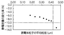
(i) 容量温度特性は、得られたコンデンサのサンプルに対し、−55〜150℃の温度範囲で最も容量温度特性が悪くなる150℃の温度環境下での静電容量の変化率(%)を測定することにより評価した。静電容量の測定にはLCRメータを用い、周波数1kHz・入力信号レベル1Vrmsの条件下で測定した。測定結果に対しては、X8R特性(−55〜150℃、ΔC=±15%以内)を満足するか否かで評価し、満足するものを○、満足しないものを×とした。その結果を表1と図2に示した。 (i) Capacitance-temperature characteristics are the rate of change in capacitance (%) in a temperature environment of 150 ° C. where the capacitance-temperature characteristics are worst in the temperature range of −55 to 150 ° C. with respect to the obtained capacitor sample Was evaluated by measuring. The capacitance was measured using an LCR meter under the conditions of a frequency of 1 kHz and an input signal level of 1 Vrms. For the measurement results, evaluation was made based on whether or not the X8R characteristics (−55 to 150 ° C., ΔC = within ± 15%) were satisfied. The results are shown in Table 1 and FIG.
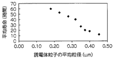
表1及び図2の結果から明らかなように、誘電体粒子(焼結後の誘電体粒子)の平均粒径が0.25μm〜0.45μmの範囲内で静電容量の変化率が15%以内になっており、X8R特性を満たしているのが確認された。 As apparent from the results of Table 1 and FIG. 2, the change rate of the capacitance is 15% when the average particle diameter of the dielectric particles (dielectric particles after sintering) is in the range of 0.25 μm to 0.45 μm. It was confirmed that the X8R characteristic was satisfied.
(ii)容量の経時変化特性は、得られたコンデンサのサンプルに対し、85℃の温度環境下で7.0V/μmの直流電圧を印加した際の、1000時間経過前後の静電容量の変化率(%)を測定することにより評価した。静電容量の測定にはLCRメータを用い、1000時間前後のサンプルを周波数1kHz・入力信号レベル1Vrmsの条件下で測定し、その結果を表1及び図3に示した。測定結果に対しては、1000時間前後の静電容量の変化率が−10%以内となるか否かで評価した。 (ii) Capacitance change over time is the change in capacitance around 1000 hours when a DC voltage of 7.0 V / μm is applied to the obtained capacitor sample in a temperature environment of 85 ° C. Evaluation was made by measuring the rate (%). An LCR meter was used to measure the capacitance, and a sample of about 1000 hours was measured under conditions of a frequency of 1 kHz and an input signal level of 1 Vrms. The results are shown in Table 1 and FIG. The measurement results were evaluated based on whether or not the rate of change in capacitance around 1000 hours was within -10%.
表1及び図3の結果から明らかなように、誘電体粒子(焼結後の誘電体粒子)の平均粒径が0.18μm〜0.42μmの範囲内で容量変化率(1000時間前後)が−10%以内になっているのが確認された。 As is apparent from the results of Table 1 and FIG. 3, the rate of change in capacity (around 1000 hours) is within the average particle diameter of the dielectric particles (dielectric particles after sintering) in the range of 0.18 μm to 0.42 μm. It was confirmed that it was within -10%.
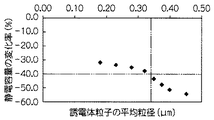
(iii) Tcバイアス特性は、得られたコンデンサのサンプルに対し、−55〜+150℃の温度条件下で、7.0V/μmの直流電圧を印加した際の静電容量の変化率(%)を測定することにより評価した。静電容量の測定にはLCRメータを用い、周波数1kHz・入力信号レベル1Vrmsの条件下で測定した。測定結果に対しては、静電容量の変化率が−40%以内となるか否かで評価した。 (iii) Tc bias characteristics are the rate of change in capacitance (%) when a DC voltage of 7.0 V / μm is applied to the obtained capacitor sample under a temperature condition of −55 to + 150 ° C. Was evaluated by measuring. The capacitance was measured using an LCR meter under the conditions of a frequency of 1 kHz and an input signal level of 1 Vrms. The measurement results were evaluated based on whether or not the rate of change in capacitance was within -40%.
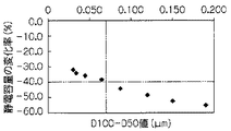
表1及び図4の結果から明らかなように、誘電体粒子(焼結後の誘電体粒子)の平均粒径が0.18μm〜0.34μmの範囲内で変化率が−40%以内になっているのが確認された。また、このTcバイアス特性について、D100−D50値との関係について調べた結果を図5に示した。図5の結果から明らかなように、D100−D50値が0.07μm以下の場合に、変化率が−40%以内になっているのが確認された。 As apparent from the results of Table 1 and FIG. 4, the change rate is within -40% when the average particle diameter of the dielectric particles (dielectric particles after sintering) is in the range of 0.18 μm to 0.34 μm. It was confirmed that Further, FIG. 5 shows the result of examining the relationship between the Tc bias characteristic and the D100-D50 value. As is clear from the results of FIG. 5, it was confirmed that the change rate was within −40% when the D100-D50 value was 0.07 μm or less.
なお、こうした結果は、誘電体粒子が小さくそのバラツキが小さいほどTcバイアス特性に優れることを示しているが、その理由については、粒子径の揃った小さい誘電体粒子で誘電体層が構成されることにより強誘電性が低減することに依存したものであると考えられる。 These results indicate that the smaller the dielectric particles and the smaller the variation, the better the Tc bias characteristics. The reason is that the dielectric layer is composed of small dielectric particles having a uniform particle diameter. This is considered to depend on the reduction in ferroelectricity.
(iv)平均寿命は、得られたコンデンサのサンプル計10個に対し、200℃の温度条件下で、15.0V/μmの直流電圧を印加した際に、抵抗が1桁変化するまでの時間で評価する加速試験を行い、その平均値(平均寿命時間)を基に評価した。抵抗値は、コンデンサの漏れ電流から計算して求めた。なお、この加速試験の結果は、得られた平均寿命時間が1.5時間以上であれば、積層型セラミックコンデンサとして十分な信頼性を有するものとして評価される。 (iv) The average lifetime is the time until the resistance changes by an order of magnitude when a DC voltage of 15.0 V / μm is applied to a total of 10 obtained capacitor samples under a temperature condition of 200 ° C. The acceleration test evaluated in (1) was performed, and the evaluation was made based on the average value (average life time). The resistance value was calculated from the leakage current of the capacitor. The result of this accelerated test is evaluated as having sufficient reliability as a multilayer ceramic capacitor if the obtained average life time is 1.5 hours or more.
表1及び図6の結果から明らかなように、この実験で得られたサンプルはいずれも1.5時間以上の平均寿命を示しており、積層型セラミックコンデンサとして十分な信頼性を有している。 As is apparent from the results in Table 1 and FIG. 6, all the samples obtained in this experiment have an average life of 1.5 hours or more, and have sufficient reliability as a multilayer ceramic capacitor. .

(v) 以上の結果から明らかなように、誘電体層を構成する誘電体粒子の平均粒子径が異なるサンプルで各特性を評価した結果、誘電体粒子(焼結後の誘電体粒子)の平均粒径が0.25〜0.42μmの範囲で、150℃の温度環境下での静電容量の変化率(%)が15%以内になると共に1000時間後の容量の経時変化率が−10%以内となり、且つX8R特性を満たした。また、誘電体粒子(焼結後の誘電体粒子)の平均粒径が0.25〜0.34μmの範囲で、150℃の温度環境下での静電容量の変化率(%)が15%以内になると共にTcバイアス時の容量変化率が−40%以内となり、且つX8R特性を満たした。また、誘電体層を構成する誘電体粒子(焼結後の誘電体粒子)のD100−D50値が0.07μm以下で、Tcバイアス時の容量の変化率が−40%以内となった。 (v) As is clear from the above results, the characteristics of the dielectric particles constituting the dielectric layer were evaluated using samples with different average particle diameters. As a result, the average of the dielectric particles (dielectric particles after sintering) When the particle size is in the range of 0.25 to 0.42 μm, the change rate (%) of the capacitance under a temperature environment of 150 ° C. is within 15%, and the change rate with time of the capacitance after 1000 hours is −10 % And satisfy the X8R characteristics. In addition, when the average particle size of the dielectric particles (dielectric particles after sintering) is in the range of 0.25 to 0.34 μm, the change rate (%) of the capacitance in a temperature environment of 150 ° C. is 15%. The capacitance change rate during Tc bias was within -40%, and the X8R characteristic was satisfied. In addition, the D100-D50 value of the dielectric particles (dielectric particles after sintering) constituting the dielectric layer was 0.07 μm or less, and the rate of change in capacitance at Tc bias was within −40%.
1…積層型セラミックコンデンサ
2…誘電体層
3…内部電極層
4…外部電極
10…積層誘電体素子本体
DESCRIPTION OF
Claims (6)
前記誘電体層を構成する前記結晶粒子の平均粒径が0.25μm以上0.42μm以下であることを特徴とする積層型セラミックコンデンサ。 A main component containing barium titanate, a first subcomponent consisting of at least one selected from MgO, CaO, BaO, and SrO, and an oxide of R (where R is from Y, Dy, Ho, and Er) At least one selected from the group consisting of at least one second subcomponent, and the ratio of the first subcomponent and the second subcomponent to 100 mol of the barium titanate is 1 mol of the first subcomponent: Dielectric layers composed of sintered bodies composed of crystal grains of a dielectric ceramic composition that exceeds 1 mol and less than 0.1 mol, and the second subcomponent exceeds 1 mol and less than 7 mol, and internal electrode layers alternately A multilayer ceramic capacitor having a laminated body,
The multilayer ceramic capacitor, wherein an average particle diameter of the crystal grains constituting the dielectric layer is 0.25 μm or more and 0.42 μm or less.
6. The difference (D100-D50) between the maximum particle size (D100) and the average particle size (D50) of the crystal particles constituting the dielectric layer is 0.07 μm or less. The multilayer ceramic capacitor according to any one of claims.
Priority Applications (1)
| Application Number | Priority Date | Filing Date | Title |
|---|---|---|---|
| JP2004102423A JP2005294290A (en) | 2004-03-31 | 2004-03-31 | Multilayered ceramic capacitor |
Applications Claiming Priority (1)
| Application Number | Priority Date | Filing Date | Title |
|---|---|---|---|
| JP2004102423A JP2005294290A (en) | 2004-03-31 | 2004-03-31 | Multilayered ceramic capacitor |
Publications (1)
| Publication Number | Publication Date |
|---|---|
| JP2005294290A true JP2005294290A (en) | 2005-10-20 |
Family
ID=35326930
Family Applications (1)
| Application Number | Title | Priority Date | Filing Date |
|---|---|---|---|
| JP2004102423A Withdrawn JP2005294290A (en) | 2004-03-31 | 2004-03-31 | Multilayered ceramic capacitor |
Country Status (1)
| Country | Link |
|---|---|
| JP (1) | JP2005294290A (en) |
Cited By (4)
| Publication number | Priority date | Publication date | Assignee | Title |
|---|---|---|---|---|
| US8358494B2 (en) | 2009-06-30 | 2013-01-22 | Murata Manufacturing Co., Ltd. | Dielectric ceramic and manufacturing method therefor and laminated ceramic capacitor |
| KR20180015079A (en) | 2016-08-02 | 2018-02-12 | 다이요 유덴 가부시키가이샤 | Multilayer ceramic capacitor |
| CN114388267A (en) * | 2022-01-12 | 2022-04-22 | 山东国瓷功能材料股份有限公司 | A kind of dielectric material for multilayer ceramic capacitor and preparation method thereof |
| CN116239378A (en) * | 2023-03-16 | 2023-06-09 | 福州大学 | A low-cost, low-loss and temperature ultra-stable dielectric material and its preparation method |
-
2004
- 2004-03-31 JP JP2004102423A patent/JP2005294290A/en not_active Withdrawn
Cited By (6)
| Publication number | Priority date | Publication date | Assignee | Title |
|---|---|---|---|---|
| US8358494B2 (en) | 2009-06-30 | 2013-01-22 | Murata Manufacturing Co., Ltd. | Dielectric ceramic and manufacturing method therefor and laminated ceramic capacitor |
| KR20180015079A (en) | 2016-08-02 | 2018-02-12 | 다이요 유덴 가부시키가이샤 | Multilayer ceramic capacitor |
| US10388457B2 (en) | 2016-08-02 | 2019-08-20 | Taiyo Yuden Co., Ltd. | Multilayer ceramic capacitor |
| CN114388267A (en) * | 2022-01-12 | 2022-04-22 | 山东国瓷功能材料股份有限公司 | A kind of dielectric material for multilayer ceramic capacitor and preparation method thereof |
| CN116239378A (en) * | 2023-03-16 | 2023-06-09 | 福州大学 | A low-cost, low-loss and temperature ultra-stable dielectric material and its preparation method |
| CN116239378B (en) * | 2023-03-16 | 2023-12-19 | 福州大学 | A low-cost, low-loss and temperature-super-stable dielectric material and its preparation method |
Similar Documents
| Publication | Publication Date | Title |
|---|---|---|
| JP4203452B2 (en) | Manufacturing method of multilayer ceramic capacitor | |
| JP3760364B2 (en) | Dielectric porcelain composition and electronic component | |
| CN1978382B (en) | Dielectric ceramic composition and electronic component | |
| JP3878778B2 (en) | Dielectric porcelain composition and electronic component | |
| JP4572628B2 (en) | Dielectric ceramic composition and electronic component | |
| JP3340722B2 (en) | Method for producing dielectric porcelain composition | |
| JP3341003B2 (en) | Dielectric porcelain composition and electronic component | |
| US7307828B2 (en) | Electronic device, dielectric ceramic composition, and method of production of the same | |
| JP4821357B2 (en) | Electronic component, dielectric ceramic composition and method for producing the same | |
| KR100807774B1 (en) | Laminated ceramic capacitor | |
| WO2002051770A1 (en) | Dielectric porcelain composition and electronic parts | |
| JP2003277139A (en) | Dielectric ceramic composition and electronic parts | |
| JP5017792B2 (en) | Electronic component, dielectric ceramic composition and method for producing the same | |
| JP4275036B2 (en) | Dielectric ceramic composition and electronic component | |
| JP2007131476A (en) | Dielectric ceramic composition, electronic component and multilayer ceramic capacitor | |
| JP2007153631A (en) | Dielectric ceramic composition, electronic component and laminated ceramic capacitor | |
| JP5017770B2 (en) | Dielectric porcelain composition and electronic component | |
| JP2007022819A (en) | Dielectric porcelain composition and electronic parts | |
| JP5167579B2 (en) | Dielectric ceramic composition and electronic component | |
| JP4487476B2 (en) | Dielectric porcelain composition and electronic component | |
| JP2005263508A (en) | Dielectric ceramic composition, laminated porcelain capacitor, and method for producing the capacitor | |
| JP4387990B2 (en) | Dielectric ceramic composition and electronic component | |
| JP4556607B2 (en) | Dielectric ceramic composition and electronic component | |
| JP2005294290A (en) | Multilayered ceramic capacitor | |
| JP4682559B2 (en) | Dielectric ceramic composition and electronic component |
Legal Events
| Date | Code | Title | Description |
|---|---|---|---|
| A300 | Withdrawal of application because of no request for examination |
Free format text: JAPANESE INTERMEDIATE CODE: A300 Effective date: 20070605 |