JP2005294091A - Nonaqueous electrolyte secondary battery electrode - Google Patents
Nonaqueous electrolyte secondary battery electrode Download PDFInfo
- Publication number
- JP2005294091A JP2005294091A JP2004108829A JP2004108829A JP2005294091A JP 2005294091 A JP2005294091 A JP 2005294091A JP 2004108829 A JP2004108829 A JP 2004108829A JP 2004108829 A JP2004108829 A JP 2004108829A JP 2005294091 A JP2005294091 A JP 2005294091A
- Authority
- JP
- Japan
- Prior art keywords
- thin film
- electrode
- current collector
- electrolyte secondary
- electron beam
- Prior art date
- Legal status (The legal status is an assumption and is not a legal conclusion. Google has not performed a legal analysis and makes no representation as to the accuracy of the status listed.)
- Pending
Links
Images

Classifications
-
- Y—GENERAL TAGGING OF NEW TECHNOLOGICAL DEVELOPMENTS; GENERAL TAGGING OF CROSS-SECTIONAL TECHNOLOGIES SPANNING OVER SEVERAL SECTIONS OF THE IPC; TECHNICAL SUBJECTS COVERED BY FORMER USPC CROSS-REFERENCE ART COLLECTIONS [XRACs] AND DIGESTS
- Y02—TECHNOLOGIES OR APPLICATIONS FOR MITIGATION OR ADAPTATION AGAINST CLIMATE CHANGE
- Y02E—REDUCTION OF GREENHOUSE GAS [GHG] EMISSIONS, RELATED TO ENERGY GENERATION, TRANSMISSION OR DISTRIBUTION
- Y02E60/00—Enabling technologies; Technologies with a potential or indirect contribution to GHG emissions mitigation
- Y02E60/10—Energy storage using batteries
Landscapes
- Cell Electrode Carriers And Collectors (AREA)
- Secondary Cells (AREA)
- Battery Electrode And Active Subsutance (AREA)
Abstract
【課題】集電体として使用する金属箔上に薄膜を形成する際の集電体表面の清浄化処理により、処理前後での金属箔の表面形状が変化し、その結果、シリコン薄膜と集電体である金属箔との密着強度が低下する。
【解決手段】集電体と、前記集電体上に堆積され、電気化学的または化学的にリチウムを吸蔵・放出する活物質からなる薄膜とを備えた非水電解質二次電池用電極において、前記集電体は前記薄膜の堆積前に電子線照射を受けた表面を有する金属箔から構成される非水電解質二次電池用電極とする。
【選択図】なし[PROBLEMS] To clean the surface of a current collector when forming a thin film on a metal foil used as a current collector, the surface shape of the metal foil before and after the treatment is changed. The adhesion strength with the metal foil as a body is reduced.
In an electrode for a nonaqueous electrolyte secondary battery, comprising: a current collector; and a thin film made of an active material deposited on the current collector and electrochemically or chemically absorbing and releasing lithium. The current collector is an electrode for a nonaqueous electrolyte secondary battery composed of a metal foil having a surface that has been irradiated with an electron beam before deposition of the thin film.
[Selection figure] None
Description
本発明は非水電解質二次電池用電極に関するものである。 The present invention relates to an electrode for a nonaqueous electrolyte secondary battery.
近年、高エネルギー密度を有するリチウムイオンを用いた非水電解質二次電池が注目を集めている。その中でも特許文献1に開示されているように、負極活物質としてシリコンあるいはその合金を用いる非水電解質二次電池が盛んに研究開発されている。しかし、これらの負極活物質は充放電に伴う膨張収縮が大きく、サイクル特性が悪い。この課題を解決するために、例えば特許文献2にはシリコン薄膜を形成する際、集電体として粗面化されたものを用いることで、サイクル特性が向上できることが開示されている。さらに、特許文献2には粗面化された集電体に対してプラズマにより形成したイオンを衝突させることで、サイクル特性が向上できることが開示されている。これらの手法により、50サイクル時点で初期容量の約90%が維持されている。いずれもが、集電体上にシリコン薄膜を密着性よく形成することができるためである。
集電体上に薄膜を形成する際に、まず集電体表面の清浄化が必要である。この目的のために、有機溶剤や蒸留水による洗浄、あるいはプラズマを真空中等で表面に照射する処理が行われる。例えば、特許文献2ではアルゴンプラズマを照射する例が記載されている。しかしながら、この手法のトレースを行ったところ、100サイクル時点での初期容量に対する容量維持率が約80%まで低下し、サイクル特性が実用上、不十分であることが明らかとなった。その原因は、シリコン薄膜と集電体である銅箔との密着強度が低下しているためであった。さらに解析を進めた結果、表面処理前後での銅箔の表面形状が変化し、その結果として密着強度が低下していることが明らかとなった。
When forming a thin film on a current collector, it is necessary to first clean the current collector surface. For this purpose, cleaning with an organic solvent or distilled water or treatment of irradiating the surface with plasma in a vacuum or the like is performed. For example,
本発明は、前記従来の課題を解決するもので、薄膜の堆積前に電子線照射を受けた表面を有する金属箔を集電体として使用することで、薄膜と集電体との密着性を向上させることを目的とする。 The present invention solves the above-mentioned conventional problems, and by using a metal foil having a surface that has been irradiated with an electron beam before deposition of the thin film as a current collector, the adhesion between the thin film and the current collector is improved. The purpose is to improve.
本発明の非水電解質二次電池用電極は、集電体と前記集電体上に堆積され、電気化学的又は化学的にリチウムを吸蔵・放出する活物質からなる薄膜とを備えた非水電解質二次電池用電極であり、前記集電体は、前記薄膜の堆積前に電子線照射を受けた表面を有する金属箔から構成されている。 An electrode for a non-aqueous electrolyte secondary battery according to the present invention includes a current collector and a thin film made of an active material deposited on the current collector and electrochemically or chemically absorbing and releasing lithium. It is an electrode for an electrolyte secondary battery, and the current collector is composed of a metal foil having a surface that has been irradiated with an electron beam before deposition of the thin film.
電子線照射はプラズマ照射と比較して、電子の質量が小さいために集電体表面に対するエッチング効果が小さい。その一方で、表面洗浄効果、特に表面に存在する有機物の除去に関する効果はほぼ同じである。従って、電子線照射を行った集電体を用いた電極は、電子線照射前後での表面形状の変化が少ないので、活物質であるシリコン薄膜との密着性がよく、充放電サイクルによる膨張収縮から生じるひずみに耐えることができる。その結果、実用的なサイクル特性が確保できる。 Electron beam irradiation has a smaller etching effect on the current collector surface because the mass of electrons is smaller than plasma irradiation. On the other hand, the surface cleaning effect, particularly the effect relating to the removal of organic substances present on the surface is almost the same. Therefore, the electrode using the current collector irradiated with the electron beam has little change in the surface shape before and after the electron beam irradiation, and thus has good adhesion to the silicon thin film as the active material, and expands and contracts due to the charge / discharge cycle. It can withstand the strain that results from As a result, practical cycle characteristics can be ensured.
本発明によれば、集電体は電子線照射処理がされる前の表面形状が電子線照射処理後も維持されるため、薄膜と集電体との密着性が向上し、プラズマ照射を行った集電体を用いた場合よりもサイクル特性を向上させることができる。 According to the present invention, since the surface shape of the current collector before the electron beam irradiation treatment is maintained after the electron beam irradiation treatment, the adhesion between the thin film and the current collector is improved, and the plasma irradiation is performed. The cycle characteristics can be improved as compared with the case where the current collector is used.
以下、本発明の実施の形態について説明する。 Embodiments of the present invention will be described below.
(実施の形態1)
本発明で用いる集電体の表面形状は、例えば、表面粗さRaおよび局部山頂の平均間隔Sで規定できる。表面粗さRaは、日本工業規格(JIS B 0601−1994)に定められた方法により表面形状測定器などを用いて測定できるが、本発明においては表面粗さRaの値は特に限定されない。集電体の材質は、銅および銅合金からなる群から選択された少なくとも1種類から構成された金属箔であることが特に好ましい。
(Embodiment 1)
The surface shape of the current collector used in the present invention can be defined by, for example, the surface roughness Ra and the average interval S between the local peaks. The surface roughness Ra can be measured using a surface shape measuring instrument or the like by a method defined in Japanese Industrial Standards (JIS B 0601-1994), but the value of the surface roughness Ra is not particularly limited in the present invention. The current collector is particularly preferably a metal foil composed of at least one selected from the group consisting of copper and copper alloys.
電子線照射された集電体は、例えば負の高電圧が印加された熱陰極とアノード電極、および必要に応じて、電子線を絞るための集束コイルや、均一な電子線照射を行うための走査コイルなどから構成される電子線照射ユニットを用いて、真空中あるいは還元性ガス雰囲気下で上記集電体に電子線を照射することによって作製できる。 The current collector irradiated with the electron beam includes, for example, a hot cathode and an anode electrode to which a negative high voltage is applied, and a focusing coil for narrowing the electron beam as required, and a uniform electron beam irradiation. It can be produced by irradiating the current collector with an electron beam in a vacuum or in a reducing gas atmosphere using an electron beam irradiation unit composed of a scanning coil or the like.
本発明では、活物質としてシリコン、ゲルマニウムおよび錫からなる群から選択された少なくとも1種類を主成分とすることが容量の観点から好ましい。その中でも、シリコンが集電体との密着性の観点から特に好ましい。 In the present invention, it is preferable from the viewpoint of capacity that the active material is mainly composed of at least one selected from the group consisting of silicon, germanium and tin. Among these, silicon is particularly preferable from the viewpoint of adhesion to the current collector.
シリコンは結晶性の違いにより、非晶質シリコン、微結晶シリコン、多結晶シリコン、および単結晶シリコンに大別される。本発明では、非晶質シリコンおよび微結晶シリコンが膨張収縮が小さいために好ましい。シリコン薄膜の結晶性はラマン分光分析により同定できる。非晶質シリコンは、ラマン分光分析において520cm−1近傍のピークが検出されないものである。なお、このピークは結晶領域に対応する。微結晶シリコンは、ラマン分光分析において、結晶領域に対応する520cm−1近傍のピークと、非晶質領域に対応する480cm−1近傍のピークの両方が検出されるものである。従って、微結晶シリコンは結晶領域と非晶質領域とから構成される。本発明においては、微結晶シリコンは520cm−1近傍のピーク強度に対する480cm−1近傍のピーク強度比(480cm−1近傍/520cm−1近傍)が0.1以上のものを言う。多結晶シリコンおよび単結晶シリコンは、ラマン分光分析において、非晶質領域に対応する480cm−1近傍のピークが検出されない。 Silicon is roughly classified into amorphous silicon, microcrystalline silicon, polycrystalline silicon, and single crystal silicon depending on the difference in crystallinity. In the present invention, amorphous silicon and microcrystalline silicon are preferable because of small expansion and contraction. The crystallinity of the silicon thin film can be identified by Raman spectroscopy. In amorphous silicon, a peak in the vicinity of 520 cm −1 is not detected in Raman spectroscopic analysis. This peak corresponds to the crystal region. In microcrystalline silicon, both a peak near 520 cm −1 corresponding to a crystalline region and a peak near 480 cm −1 corresponding to an amorphous region are detected in Raman spectroscopic analysis. Therefore, microcrystalline silicon is composed of a crystalline region and an amorphous region. In the present invention, microcrystalline silicon 520 cm -1 480 cm -1 peak intensity ratio near to the peak intensity in the vicinity (480 cm -1 vicinity / 520 cm -1 vicinity) refers to more than 0.1. In polycrystalline silicon and single crystal silicon, a peak in the vicinity of 480 cm −1 corresponding to an amorphous region is not detected in Raman spectroscopic analysis.
集電体上にシリコン薄膜を形成するための手法としては、CVD法、スパッタリング法、蒸着法、溶射法および焼結法が適用できる。 As a method for forming a silicon thin film on the current collector, a CVD method, a sputtering method, a vapor deposition method, a thermal spraying method, and a sintering method can be applied.
以下、本発明の実施例について図面を参照しながら説明する。なお、実施例において、集電体の表面粗さの測定、シリコンの結晶性およびサイクル特性の測定は下記のようにして行った。 Embodiments of the present invention will be described below with reference to the drawings. In the examples, the measurement of the surface roughness of the current collector and the measurement of the crystallinity and cycle characteristics of silicon were performed as follows.
銅箔の表面粗さRaは、日本工業規格(JIS B 0601−1994)に定められた方法により、触針式表面形状測定器Dektak ST(日本真空技術社製)を用い、測定距離を2.0mmに設定して測定した。表面粗さRaの計算は、たわみ分の補正後に行った。たわみ分の補正に用いた補正値は、ローパス=200μm、ハイパス=20μmである。なお、表面粗さRaは自動計算された値である。 The surface roughness Ra of the copper foil is measured according to a method defined in Japanese Industrial Standard (JIS B 0601-1994) using a stylus type surface shape measuring device Dektak ST (manufactured by Nippon Vacuum Technology Co., Ltd.). Measurements were made at 0 mm. The calculation of the surface roughness Ra was performed after correcting the deflection. The correction values used for correcting the deflection are low-pass = 200 μm and high-pass = 20 μm. The surface roughness Ra is an automatically calculated value.
(1)集電体の作製
図1は電子線照射から薄膜製造の工程を模式的に示す装置概略図である。図1に示すように、電子線照射は電子線照射装置10から、負極集電体である銅箔基板20に電子線を照射することによって行った。電子線照射装置10の対向面上を銅箔基板20が通過することにより、連続的に電子線照射処理を行うことが出来る。熱陰極への印加電圧は−2V〜−20kVとし、電子線のエミッション電流は0.02mA/cm2〜5mA/cm2の範囲とした。
(1) Production of Current Collector FIG. 1 is a schematic view of an apparatus schematically showing steps from electron beam irradiation to thin film production. As shown in FIG. 1, the electron beam irradiation was performed by irradiating the electron
(2)シリコン薄膜の製膜方法
集電体である銅箔基板20上にシリコン薄膜22を形成するために、本発明では蒸着法を用いた。シリコン薄膜22の厚みは4μmとした。蒸着のための蒸着成膜源40には電子ビームを使用し、概ね0.15μm/sでシリコン薄膜22を堆積させた。ガス導入前の真空度は5×10−3Paで、これにさらに水素ガスを微量導入して蒸着を行った。水素ガスの導入量は0.09Pa・m3/sとした。このシリコン薄膜22のラマン分光分析を行ったところ、520cm−1近傍のピークが検出されなかったことから、非晶質であることが分かった。一方、堆積速度を0.1μm/hrとし、円筒状ローラ15の温度を300℃とした場合のシリコン薄膜に対してラマン分光分析を行ったところ、520cm−1近傍のピークと480cm−1近傍のピークの両方が検出され、ピーク強度比(480cm−1近傍/520cm−1近傍)は0.4であった。従って、この条件で作成したシリコン薄膜は微結晶であることが分かった。
(2) Method for Forming Silicon Thin Film In order to form the silicon
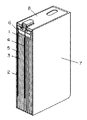
(3)試験電池の作り方およびサイクル電特性の評価法
以下に、試験用扁平形電池(試験セル)の作製方法を図2の扁平形電池の縦断面図とともに説明する。
(3) How to make test battery and evaluation method of cycle electric characteristics A method for producing a test flat battery (test cell) will be described below together with a longitudinal sectional view of the flat battery in FIG.
まず、正極1の作製方法について説明する。正極活物質(図示せず)であるLiCoO2は、Li2CO3とCoCO3とを所定のモル比で混合し、950℃で加熱することによって合成した。さらに、これを100メッシュ以下の大きさに分級したものを用いた。正極活物質100gに対して、導電剤としてアセチレンブラックを10g、結着剤としてポリ4フッ化エチレンの水性分散液8g(樹脂成分)および純水を加えて充分に混合し、正極合剤ペースト(図示せず)を得た。このペーストをアルミニウムの芯材に塗布・乾燥し、圧延して正極1を得た。 First, a method for manufacturing the positive electrode 1 will be described. LiCoO 2 which is a positive electrode active material (not shown) was synthesized by mixing Li 2 CO 3 and CoCO 3 at a predetermined molar ratio and heating at 950 ° C. Furthermore, what classify | categorized this into the magnitude | size of 100 mesh or less was used. To 100 g of the positive electrode active material, 10 g of acetylene black as a conductive agent, 8 g of an aqueous dispersion of polytetrafluoroethylene (resin component) and pure water as a binder are added and mixed well, and a positive electrode mixture paste ( (Not shown). This paste was applied to an aluminum core, dried, and rolled to obtain a positive electrode 1.
次に、超音波溶接で、先に得られた正極1にアルミニウムからなる正極リード2を取り付けた。同様にして得られた負極3に銅の負極リード4を取り付けた。そして、正極1、負極3、および両電極より幅が広く帯状の多孔性ポリプロピレン製セパレータ5を積層した。このとき、両電極の間に前記セパレータ5を介在させた。次いで、積層物を扁平状に捲回して電極群とした。
Next, the
上記電極群の上下に、それぞれポリプロピレン製の絶縁板を配して、電池ケース7に挿入した。そして、電池ケース7の上部に枠体6を形成した後、所定の非水電解液(1.0モル/LのLiPF6を含むエチレンカーボネート(EC)+ジエチルカーボネート(DEC)(1:3体積比混合溶媒))を注入し、正極端子を有する封口板8で密閉して扁平形電池とした。
Polypropylene insulating plates were arranged above and below the electrode group, and inserted into the
試験セルのサイクル特性評価は20℃の条件下で以下のように実施した。まず、試験セルの定電流充電を、充電電流0.2C(1Cは1時間率電流)で電池電圧が4.2Vになるまで行い、次いで定電圧充電を4.2V、電流値が0.01Cになるまで行った。その後、試験セルの放電を、0.2Cの電流で電池電圧が2.5Vになるまで行った。容量維持率(%)とは、1サイクル目の放電容量に対する、あるサイクル数での放電容量の割合である。 The cycle characteristics of the test cell were evaluated as follows under the condition of 20 ° C. First, constant current charging of the test cell is performed until the battery voltage reaches 4.2 V at a charging current of 0.2 C (1 C is a 1 hour rate current), and then constant voltage charging is 4.2 V and the current value is 0.01 C. I went until. Thereafter, the test cell was discharged at a current of 0.2 C until the battery voltage reached 2.5V. The capacity retention rate (%) is the ratio of the discharge capacity at a certain number of cycles to the discharge capacity at the first cycle.
(実施例1)
図1の電子線照射装置において、厚さ20μmの電解銅箔を集電体として用いた。この銅箔に対して10−3Paの真空中において、印加電圧は−50Vとし、電子線のエミッション電流は0.02mA/cm2として10分間電子線照射を行った。次に、この銅箔を用いて非晶質となる製膜条件下でシリコン薄膜を2μm堆積して電極を作製した。この電極を用いて電池を作製し、サイクル特性を測定して放電維持率が80%となるサイクル数を求めた。
(Example 1)
In the electron beam irradiation apparatus of FIG. 1, an electrolytic copper foil having a thickness of 20 μm was used as a current collector. The copper foil was irradiated with an electron beam for 10 minutes in a vacuum of 10 −3 Pa at an applied voltage of −50 V and an emission current of the electron beam of 0.02 mA / cm 2 . Next, 2 μm of a silicon thin film was deposited on the copper foil under an amorphous film forming condition to produce an electrode. A battery was fabricated using this electrode, and the cycle characteristics were measured to determine the number of cycles at which the discharge retention rate was 80%.
(実施例2)
図1の電子線照射装置において、水素ガスを導入して10−2Paの圧力となるように調整しながら電子線照射を行った。これ以外は、実施例1と同様にして放電維持率が80%となるサイクル数を求めた。
(Example 2)
In the electron beam irradiation apparatus of FIG. 1, electron beam irradiation was performed while introducing hydrogen gas and adjusting the pressure to 10 −2 Pa. Except for this, the number of cycles at which the discharge retention rate was 80% was determined in the same manner as in Example 1.
(実施例3)
実施例1と同様の手法により銅箔に対して電子線照射を行った。次に、この銅箔を用いて微結晶となる製膜条件下でシリコン薄膜を2μm堆積して電極を作製した。この電極を用いて電池を作製し、サイクル特性を測定して放電維持率が80%となるサイクル数を求めた。
(Example 3)
The copper foil was irradiated with an electron beam by the same method as in Example 1. Next, 2 μm of a silicon thin film was deposited under the film-forming conditions for forming microcrystals using this copper foil, thereby producing an electrode. A battery was fabricated using this electrode, and the cycle characteristics were measured to determine the number of cycles at which the discharge retention rate was 80%.
(実施例4)
実施例2と同様の手法により得られた銅箔を用いて、実施例3と同様の条件でシリコン薄膜を作製した。この電極を用いて電池を作製し、サイクル特性を測定して放電維持率が80%となるサイクル数を求めた。
Example 4
A silicon thin film was produced under the same conditions as in Example 3 using a copper foil obtained by the same method as in Example 2. A battery was fabricated using this electrode, and the cycle characteristics were measured to determine the number of cycles at which the discharge retention rate was 80%.
(比較例1)
図1において、電子線照射装置の代わりにプラズマ源を設置し、ECRアルゴンプラズマを発生させ、マイクロ波電力200W、アルゴンガス分圧0.06Paで10分間、実施例1で用いた銅箔に対してプラズマ照射を行った。これ以外は、実施例1と同様の手法により電池を作製し、放電維持率が80%となるサイクル数を求めた。
(Comparative Example 1)
In FIG. 1, a plasma source is installed in place of the electron beam irradiation apparatus, ECR argon plasma is generated, microwave power 200 W, argon gas partial pressure 0.06 Pa for 10 minutes, and the copper foil used in Example 1 Then, plasma irradiation was performed. Except for this, a battery was produced in the same manner as in Example 1, and the number of cycles at which the discharge retention rate was 80% was determined.
(比較例2)
比較例1で作製したプラズマ照射された銅箔を用い、実施例3と同様の手法によりシリコン薄膜を堆積させて電極とした。この電極を用いて、実施例1と同様の手法により電池を作製して放電維持率が80%となるサイクル数を求めた。
(Comparative Example 2)
Using the plasma-irradiated copper foil produced in Comparative Example 1, a silicon thin film was deposited by the same method as in Example 3 to obtain an electrode. Using this electrode, a battery was produced in the same manner as in Example 1, and the number of cycles at which the discharge retention rate was 80% was determined.
上記実施例および比較例の結果を(表1)および(表2)にまとめた。 The results of the above Examples and Comparative Examples are summarized in (Table 1) and (Table 2).

これらの結果、本発明による電極を用いることにより、従来よりも実用的なサイクル特性をもつ電極を得ることができる。 As a result, by using the electrode according to the present invention, an electrode having more practical cycle characteristics than before can be obtained.
本発明にかかる電極は電子線照射を受けた表面を有する金属箔から構成されており、非水電解質二次電池用電極等として有用である。 The electrode according to the present invention is composed of a metal foil having a surface irradiated with an electron beam, and is useful as an electrode for a nonaqueous electrolyte secondary battery.
1 正極
2 正極リード
3 負極
4 負極リード
5 セパレータ
6 枠体
7 電池ケース
8 封口板
10 電子線照射装置
11 巻き出しロール
12 搬送ロール
13 巻き取りロール
15 円筒状ローラ
20 銅箔基板
22 シリコン薄膜
30 真空槽
32 排気ポンプ
34 ガス導入管
36 マスク
40 蒸着成膜源
45 仕切り
DESCRIPTION OF SYMBOLS 1
Claims (6)
請求項1に記載の非水電解質二次電池用電極。 The metal foil has a surface that has been subjected to electron beam irradiation in vacuum prior to the deposition of the thin film,
The electrode for nonaqueous electrolyte secondary batteries according to claim 1.
請求項1に記載の非水電解質二次電池用電極。 The metal foil has a surface that has been irradiated with an electron beam in a reducing gas atmosphere before the thin film is deposited,
The electrode for nonaqueous electrolyte secondary batteries according to claim 1.
請求項1から3のいずれかに記載の非水電解質二次電池用電極。 The metal foil is composed of at least one selected from the group consisting of copper and copper alloys,
The electrode for nonaqueous electrolyte secondary batteries in any one of Claim 1 to 3.
請求項1から4のいずれかに記載の非水電解質二次電池用電極。 The thin film has at least one selected from the group consisting of silicon, germanium, and tin.
The electrode for nonaqueous electrolyte secondary batteries in any one of Claim 1 to 4.
請求項1から4のいずれかに記載の非水電解質二次電池用電極。 The thin film is made of microcrystalline silicon or amorphous silicon,
The electrode for nonaqueous electrolyte secondary batteries in any one of Claim 1 to 4.
Priority Applications (1)
| Application Number | Priority Date | Filing Date | Title |
|---|---|---|---|
| JP2004108829A JP2005294091A (en) | 2004-04-01 | 2004-04-01 | Nonaqueous electrolyte secondary battery electrode |
Applications Claiming Priority (1)
| Application Number | Priority Date | Filing Date | Title |
|---|---|---|---|
| JP2004108829A JP2005294091A (en) | 2004-04-01 | 2004-04-01 | Nonaqueous electrolyte secondary battery electrode |
Publications (1)
| Publication Number | Publication Date |
|---|---|
| JP2005294091A true JP2005294091A (en) | 2005-10-20 |
Family
ID=35326783
Family Applications (1)
| Application Number | Title | Priority Date | Filing Date |
|---|---|---|---|
| JP2004108829A Pending JP2005294091A (en) | 2004-04-01 | 2004-04-01 | Nonaqueous electrolyte secondary battery electrode |
Country Status (1)
| Country | Link |
|---|---|
| JP (1) | JP2005294091A (en) |
Cited By (2)
| Publication number | Priority date | Publication date | Assignee | Title |
|---|---|---|---|---|
| JP2007165293A (en) * | 2005-11-16 | 2007-06-28 | Jfe Chemical Corp | Lithium ion secondary battery negative electrode, method for producing the same, and lithium ion secondary battery |
| JP2007265878A (en) * | 2006-03-29 | 2007-10-11 | Sanyo Electric Co Ltd | Method of manufacturing electrode for lithium secondary battery, and lithium secondary battery |
Citations (5)
| Publication number | Priority date | Publication date | Assignee | Title |
|---|---|---|---|---|
| JP2002083594A (en) * | 1999-10-22 | 2002-03-22 | Sanyo Electric Co Ltd | Electrode for lithium battery, lithium battery using it and lithium secondary battery |
| JP2002157999A (en) * | 2000-11-20 | 2002-05-31 | Sanyo Electric Co Ltd | Method of manufacturing electrode for secondary battery |
| JP2002190298A (en) * | 2000-12-22 | 2002-07-05 | Sanyo Electric Co Ltd | Method for manufacturing electrode for secondary cell |
| JP2003077529A (en) * | 2001-09-03 | 2003-03-14 | Sanyo Electric Co Ltd | Lithium battery and lithium secondary battery |
| JP2004074218A (en) * | 2002-08-19 | 2004-03-11 | Hitachi Metals Ltd | Method for manufacturing laminated band material |
-
2004
- 2004-04-01 JP JP2004108829A patent/JP2005294091A/en active Pending
Patent Citations (5)
| Publication number | Priority date | Publication date | Assignee | Title |
|---|---|---|---|---|
| JP2002083594A (en) * | 1999-10-22 | 2002-03-22 | Sanyo Electric Co Ltd | Electrode for lithium battery, lithium battery using it and lithium secondary battery |
| JP2002157999A (en) * | 2000-11-20 | 2002-05-31 | Sanyo Electric Co Ltd | Method of manufacturing electrode for secondary battery |
| JP2002190298A (en) * | 2000-12-22 | 2002-07-05 | Sanyo Electric Co Ltd | Method for manufacturing electrode for secondary cell |
| JP2003077529A (en) * | 2001-09-03 | 2003-03-14 | Sanyo Electric Co Ltd | Lithium battery and lithium secondary battery |
| JP2004074218A (en) * | 2002-08-19 | 2004-03-11 | Hitachi Metals Ltd | Method for manufacturing laminated band material |
Cited By (2)
| Publication number | Priority date | Publication date | Assignee | Title |
|---|---|---|---|---|
| JP2007165293A (en) * | 2005-11-16 | 2007-06-28 | Jfe Chemical Corp | Lithium ion secondary battery negative electrode, method for producing the same, and lithium ion secondary battery |
| JP2007265878A (en) * | 2006-03-29 | 2007-10-11 | Sanyo Electric Co Ltd | Method of manufacturing electrode for lithium secondary battery, and lithium secondary battery |
Similar Documents
| Publication | Publication Date | Title |
|---|---|---|
| JP4113910B2 (en) | Negative electrode for lithium secondary battery and method for producing the same | |
| JP4642835B2 (en) | Current collector for electrode | |
| KR101946658B1 (en) | Electrode foil, current collector, electrode, and electric energy storage element using same | |
| US6649033B2 (en) | Method for producing electrode for lithium secondary battery | |
| JP5334156B2 (en) | Method for producing non-aqueous electrolyte secondary battery | |
| JPWO2001029912A1 (en) | Lithium battery electrode and lithium secondary battery | |
| JPWO2001029918A1 (en) | Electrode for lithium secondary battery and lithium secondary battery | |
| JPWO2001031723A1 (en) | Electrode for lithium secondary battery and lithium secondary battery | |
| JPWO2001031721A1 (en) | Lithium battery electrode and lithium secondary battery | |
| JP4036889B2 (en) | battery | |
| CN108886150A (en) | Negative electrode for secondary battery comprising lithium metal layer having fine pattern and protective layer thereof, and method for manufacturing same | |
| JP2001266851A (en) | Manufacturing method of electrode for lithium secondary battery | |
| JP6247715B2 (en) | Power storage device | |
| JP2011216193A (en) | Negative electrode for lithium battery, and lithium secondary battery using this | |
| CN102232252A (en) | Lithium ion secondary battery negative electrode and lithium ion secondary battery | |
| JP2008117785A (en) | Negative electrode for lithium secondary battery and method for producing the same | |
| JP5058381B1 (en) | Current collector and electrode, and power storage device using the same | |
| JP2013165250A (en) | Collector and electrode, and power storage element using the same | |
| JP4512336B2 (en) | Capacitors | |
| JP5119584B2 (en) | Nonaqueous electrolyte secondary battery and method for producing the negative electrode | |
| JP2003017069A (en) | Electrode for lithium secondary battery and lithium secondary battery | |
| JP5238195B2 (en) | Negative electrode for lithium ion secondary battery and lithium ion secondary battery | |
| JP2005294091A (en) | Nonaqueous electrolyte secondary battery electrode | |
| CN105680028B (en) | A kind of sodium-ion battery negative electrode material silicon antimony alloy film and preparation method thereof | |
| JP2005327505A (en) | Electrode for lithium secondary battery |
Legal Events
| Date | Code | Title | Description |
|---|---|---|---|
| A621 | Written request for application examination |
Free format text: JAPANESE INTERMEDIATE CODE: A621 Effective date: 20060926 |
|
| RD01 | Notification of change of attorney |
Free format text: JAPANESE INTERMEDIATE CODE: A7421 Effective date: 20061012 |
|
| RD01 | Notification of change of attorney |
Free format text: JAPANESE INTERMEDIATE CODE: A7421 Effective date: 20091120 |
|
| A131 | Notification of reasons for refusal |
Free format text: JAPANESE INTERMEDIATE CODE: A131 Effective date: 20100518 |
|
| A02 | Decision of refusal |
Free format text: JAPANESE INTERMEDIATE CODE: A02 Effective date: 20100928 |