JP2005294043A - Ion implantation apparatus and ion implantation method - Google Patents
Ion implantation apparatus and ion implantation method Download PDFInfo
- Publication number
- JP2005294043A JP2005294043A JP2004107546A JP2004107546A JP2005294043A JP 2005294043 A JP2005294043 A JP 2005294043A JP 2004107546 A JP2004107546 A JP 2004107546A JP 2004107546 A JP2004107546 A JP 2004107546A JP 2005294043 A JP2005294043 A JP 2005294043A
- Authority
- JP
- Japan
- Prior art keywords
- ion implantation
- negative ion
- ions
- ion source
- source
- Prior art date
- Legal status (The legal status is an assumption and is not a legal conclusion. Google has not performed a legal analysis and makes no representation as to the accuracy of the status listed.)
- Pending
Links
Images


Landscapes
- Electron Sources, Ion Sources (AREA)
Abstract
Description
本発明は、被処理基板にイオンを注入する装置および方法に関する。 The present invention relates to an apparatus and a method for implanting ions into a substrate to be processed.
シリコン基板に酸素のイオンを注入することにより、シリコン基板の表面から所定深さの位置に埋込酸化層を形成する技術がある。 There is a technique for forming a buried oxide layer at a predetermined depth from the surface of the silicon substrate by implanting oxygen ions into the silicon substrate.
従来、埋込酸化層を形成するために、マイクロ波イオン源を用いてイオンビームを発生させ、質量分離器で酸素のプラスイオン(16O+)のビームを選別し、半導体ウエハに照射することにより、上記埋込酸化層を形成している(例えば、非特許文献1参照。)。
しかし、上記したマイクロ波イオン源を用いる方法では、生成されたイオンビームの中から酸素イオンのビームを選別するために、質量分離器等を設置しなければならず、装置全体が巨大になる。 However, in the method using the microwave ion source described above, a mass separator or the like must be installed in order to select a beam of oxygen ions from the generated ion beam, and the entire apparatus becomes huge.
また、イオンを打ち込む際、イオンを打ち込まれた半導体ウエハから二次電子が放出され、半導体ウエハはプラスに帯電する。上記したようにプラスイオンを打ち込む場合は、半導体ウエハのプラス電荷がさらに増加する。 When ions are implanted, secondary electrons are emitted from the semiconductor wafer into which ions are implanted, and the semiconductor wafer is positively charged. When positive ions are implanted as described above, the positive charge of the semiconductor wafer further increases.
このため、プラスイオンを打ち込んだ領域と打ち込んでいない領域との間では、帯電量が大きく異なり、半導体ウエハ全体における電荷分布が不均一となる。また、高いプラス電位を有する半導体ウエハは、静電気により、パーティクル等を引きつけやすい。このため、半導体ウエハの電荷を中和するための電子ビームを生成する電子源等を設置しなければならず、装置が複雑になる。 For this reason, the charge amount differs greatly between the region where the positive ions are implanted and the region where the positive ions are not implanted, and the charge distribution in the entire semiconductor wafer becomes non-uniform. In addition, a semiconductor wafer having a high positive potential tends to attract particles and the like due to static electricity. For this reason, an electron source or the like that generates an electron beam for neutralizing the charge of the semiconductor wafer must be installed, and the apparatus becomes complicated.
また、以上のように質量分離器や電子源等を設置することにより、装置全体のコストが高くなるという問題がある。 Moreover, there exists a problem that the cost of the whole apparatus becomes high by installing a mass separator, an electron source, etc. as mentioned above.
従って、本発明は、小型なイオン注入装置、および、小型なイオン注入装置を実現可能なイオン注入方法を提供することを目的とする。 Therefore, an object of the present invention is to provide a small ion implantation apparatus and an ion implantation method capable of realizing a small ion implantation apparatus.
また、本発明は、構成が簡単なイオン注入装置、および、構成が簡単なイオン注入装置を実現可能なイオン注入方法を提供することを目的とする。 Another object of the present invention is to provide an ion implantation apparatus having a simple configuration and an ion implantation method capable of realizing an ion implantation apparatus having a simple configuration.
また、本発明は、安価なイオン注入装置、および、安価なイオン注入装置を実現可能なイオン注入方法を提供することを目的とする。 Another object of the present invention is to provide an inexpensive ion implantation apparatus and an ion implantation method capable of realizing an inexpensive ion implantation apparatus.
上記目的を達成するために、本発明の第1の観点にかかるイオン注入装置は、被処理基板にイオンを注入することにより、該被処理基板の内部に酸化層を形成するイオン注入装置であって、酸素マイナスイオンラジカルを前記イオンとして、前記被処理基板に注入する、ことを特徴とする。 In order to achieve the above object, an ion implantation apparatus according to a first aspect of the present invention is an ion implantation apparatus that forms an oxide layer inside a substrate to be processed by implanting ions into the substrate to be processed. Then, oxygen negative ion radicals are implanted as the ions into the substrate to be processed.
前記イオン注入装置は、前記イオンのビームを生成するビーム生成手段と、前記ビーム生成手段が生成する前記ビームを、前記被処理基板上まで真っ直ぐに導いて照射するビーム照射手段と、から構成されてもよい。 The ion implantation apparatus includes a beam generating unit that generates a beam of the ions, and a beam irradiation unit that guides and irradiates the beam generated by the beam generating unit straight onto the substrate to be processed. Also good.
前記ビーム照射手段は、前記ビームを収束する収束レンズと、前記イオンを加速して所定エネルギーのビームを生成する加速器と、前記ビームを整形する四重極レンズと、から構成され、前記収束レンズ、前記加速器、および、前記四重極レンズの中心軸は、一直線に並んでいてもよい。 The beam irradiating means includes a converging lens for converging the beam, an accelerator for accelerating the ions to generate a beam with a predetermined energy, and a quadrupole lens for shaping the beam. The central axis of the accelerator and the quadrupole lens may be aligned.
前記ビーム生成手段は、酸素マイナスイオンラジカルを含有するマイナスイオンソースを加熱する加熱手段と、前記加熱手段によって加熱される前記マイナスイオンソースに電界を印加し、該マイナスイオンソースに含有されている前記酸素マイナスイオンラジカルを取り出すことにより、前記ビームを生成する電界印加手段と、から構成されていてもよい。 The beam generating means applies a electric field to the negative ion source heated by the heating means for heating a negative ion source containing oxygen negative ion radicals, and is contained in the negative ion source. And an electric field applying means for generating the beam by taking out oxygen negative ion radicals.
前記加熱手段は、前記マイナスイオンソースを250〜1000℃に加熱してもよい。 The heating means may heat the negative ion source to 250 to 1000 ° C.
上記加熱温度は、好ましくは400〜800℃であり、より好ましくは700〜800℃である。 The heating temperature is preferably 400 to 800 ° C, more preferably 700 to 800 ° C.
前記電界印加手段は、前記マイナスイオンソースに、100〜10000V/cmの電界を印加してもよい。 The electric field applying means may apply an electric field of 100 to 10,000 V / cm to the negative ion source.
上記電界の強さは、好ましくは200〜5000V/cmである。 The strength of the electric field is preferably 200 to 5000 V / cm.
前記マイナスイオンソースは、12CaO・7Al2O3であってもよい。 The negative ion source may be 12CaO · 7Al 2 O 3 .
本発明の第2の観点にかかるイオン注入方法は、被処理基板にイオンを注入することにより、該被処理基板の内部に酸化層を形成するイオン注入方法であって、酸素マイナスイオンラジカルを前記イオンとして、前記被処理基板に注入する工程を備える、ことを特徴とする。 An ion implantation method according to a second aspect of the present invention is an ion implantation method for forming an oxide layer inside a substrate to be processed by implanting ions into the substrate to be processed, wherein The method includes a step of implanting ions into the substrate to be processed.
本発明によって、小型で、構成が簡単な、安価なイオン注入装置およびイオン注入方法を実現することができる。 According to the present invention, an inexpensive ion implantation apparatus and ion implantation method that are small in size and simple in configuration can be realized.
次に、本発明の実施の形態にかかるイオン注入装置について図面を参照して説明する。 Next, an ion implantation apparatus according to an embodiment of the present invention will be described with reference to the drawings.
本発明の実施の形態にかかるイオン注入装置は、酸素マイナスイオンラジカル(O-)を被処理基板(半導体ウエハ)に打ち込むことにより、被処理基板の内部に埋込酸化層を形成する。 The ion implantation apparatus according to the embodiment of the present invention forms a buried oxide layer inside a substrate to be processed by implanting oxygen negative ion radicals (O − ) into the substrate to be processed (semiconductor wafer).
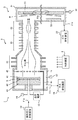
上記イオン注入装置は、図1に示すように、酸素のマイナスイオンビームを生成するイオンソース部1と、イオンソース部1で生成されたイオンビームを導くビームライン部2と、処理対象の半導体ウエハWが配置されるエンドステーション部3と、イオンソース部1、ビームライン部2、および、エンドステーション部3の動作を制御する制御装置4と、から構成される。 As shown in FIG. 1, the ion implantation apparatus includes an ion source unit 1 that generates a negative ion beam of oxygen, a beam line unit 2 that guides an ion beam generated by the ion source unit 1, and a semiconductor wafer to be processed. An end station unit 3 in which W is arranged, an ion source unit 1, a beam line unit 2, and a control device 4 that controls the operation of the end station unit 3 are configured.
イオンソース部1は、処理室(イオンビーム生成室)11と、高圧電源12と、原料ガス供給装置13と、ガス排気装置14と、から構成され、酸素マイナスイオンラジカルを発生させ、酸素のマイナスイオンビームを生成する。
The ion source unit 1 includes a processing chamber (ion beam generation chamber) 11, a high
酸素マイナスイオンラジカルは、例えば12CaO・7Al2O3から構成されるマイナスイオンソースSから発生させることができる。酸素マイナスイオンラジカルは、12CaO・7Al2O3のAlO4四面体が重合して形成するケージ内に閉じこめられており、後述するように、マイナスイオンソースSを所定温度に加熱して所定の強さの電界を印加することによって取り出される。 The oxygen negative ion radical can be generated from a negative ion source S composed of, for example, 12CaO · 7Al 2 O 3 . The oxygen negative ion radical is confined in a cage formed by polymerization of the 12CaO · 7Al 2 O 3 AlO 4 tetrahedron. As will be described later, the negative ion source S is heated to a predetermined temperature to obtain a predetermined strength. It is taken out by applying an electric field.
処理室11は、例えばアルミニウム等から形成された処理チャンバである。処理室11の壁には、マイナスイオンソースSにマイナスイオンを補充するための原料ガスを処理室11内に導入するための原料ガス供給管11aと、処理室11内のガスを排気するためのガス排気管11bと、が設置されている。
The
また、マイナスイオンは、壁にぶつかったり、他の化学種と結びついたりして、その活性を失っていく。このため、処理室11の内壁は、マイナスイオンと反応しにくいフルオロカーボン(特にPTFE;四フッ化エチレン樹脂)、または、テフロン(登録商標)等から形成される。さらに、処理室11は、マイナスイオンを引きつけないように、処理中は、接地されている、または、マイナスの電位に保持されている。
Negative ions collide with walls or bind to other chemical species and lose their activity. For this reason, the inner wall of the
処理室11の内部には、ホットプレート41と、接触電極42と、クランプ43と、電極支持部材44と、引出電極45と、が設置されている。
Inside the
ホットプレート41は、処理室11内の側壁上に設置されている。ホットプレート41は、処理室11内に配置されるマイナスイオンソースSを後述する所定温度に加熱する。ホットプレート41の内部には、上記した原料ガス供給管11aが貫通しており、原料ガス供給管11aを介して供給される原料ガスは、ホットプレート41の表面から噴出される。
The
接触電極42は、マイナスイオンソースSに貼り付けた状態で製造され、その表面がビームライン部2内を通るイオンビームの進行方向に垂直となるように、ホットプレート41上に配置される。接触電極42は、ホットプレート41の表面から噴出する原料ガスを通す大きさの貫通した空隙のある多孔質とし、原料ガスとマイナスイオンソースSと接触電極42の三相界面を有するように製造する。接触電極42の製造方法としては、例えば、微粉末を膜状に成型し焼結させたもの、もしくはスパッタリングや蒸着によって膜を堆積させる方法がある。
The
また、原料ガスとの接触面積を増やすため、接触電極42は、例えば図2に示すように、複数の開口42aを有する網状に形成してもよい。接触電極42は、電界を印加するための高圧電源12の陰極と電気的に接続されている。
Further, in order to increase the contact area with the source gas, the
接触電極42に使用可能な物質としては、(1)ジルコニア系の物質、(2)セリア系の物質、(3)ペロブスカイト型(ABO3)複酸化物にドープしたもの、(4)酸化雰囲気で安定な金属などのイオン導電性の高い物質がある。
Materials that can be used for the
上記(1)に該当する物質としては、例えば、YSZ(8mol%Y2O3-ZrO2:イットリア安定化ジルコニア)、SSZ(10mol%Sc2O3-1mol%Al2O3-ZrO2:スカンジア安定化ジルコニア)などが挙げられる。 Examples of the substance corresponding to the above (1) include YSZ (8 mol% Y 2 O 3 —ZrO 2 : yttria stabilized zirconia), SSZ (10 mol% Sc 2 O 3 −1 mol% Al 2 O 3 —ZrO 2 : Scandia-stabilized zirconia).
上記(2)に該当する物質としては、例えばGDC(20mol%GdO1.5-CeO2:ガドリニウム含有セリア)、SDC(20mol%SmO1.5-CeO2:サマリウム含有セリア)などが挙げられる。なお、これら以外に、YO1.5、GaO1.5、NbO2.5などをドープしたものでも良い。 Examples of the substance corresponding to the above (2) include GDC (20 mol% GdO 1.5 -CeO 2 : gadolinium-containing ceria), SDC (20 mol% SmO 1.5 -CeO 2 : samarium-containing ceria) and the like. In addition to these, those doped with YO 1.5 , GaO 1.5 , NbO 2.5, or the like may be used.
上記(3)に該当する物質としては、(La,Sr)MnO3:マンガン酸ランタン−ストロンチウム置換、(La,Sr)(Co,Ni,Fe)O3:コバルト酸ランタン−ストロンチウム置換、ニッケル置換、鉄置換、(La,Sr)(Ga,Mg)O3:ガリウム酸ランタン、ランタンガレート−ストロンチウム置換、マグネシウム置換、(La,Sr)(Cr,Ti,Co)O3:クロム酸ランタン−ストロンチウム置換、チタン置換、コバルト置換、La2/3(Ti0.95Al0.05)O3:チタン酸ランタン−アルミ置換などが挙げられる。なお、ランタンを別のランタノイド(La〜Eu、12配位のイオン半径が比較的大きいもの)(例えば、Sm0.5Sr0.5CoO3など)に置き換えたものでも良い。 Substances corresponding to the above (3) include (La, Sr) MnO 3 : lanthanum manganate-strontium substitution, (La, Sr) (Co, Ni, Fe) O 3 : lanthanum cobaltate-strontium substitution, nickel substitution , Iron substitution, (La, Sr) (Ga, Mg) O 3 : lanthanum gallate, lanthanum gallate-strontium substitution, magnesium substitution, (La, Sr) (Cr, Ti, Co) O 3 : lanthanum chromate-strontium Substitution, titanium substitution, cobalt substitution, La 2/3 (Ti 0.95 Al 0.05 ) O 3 : lanthanum titanate-aluminum substitution and the like. Note that lanthanum may be replaced with another lanthanoid (La to Eu, 12-coordinate ion radius is relatively large) (for example, Sm 0.5 Sr 0.5 CoO 3 or the like).
上記(4)に該当する物質としては、Pt、Au、Ag、Pdなどが挙げられる。なお、処理温度が比較的低い場合には、他の金属を接触電極42として使用することもできる。
Examples of the substance corresponding to the above (4) include Pt, Au, Ag, and Pd. If the processing temperature is relatively low, another metal can be used as the
クランプ43は、接触電極42およびマイナスイオンソースSを、ホットプレート41上に固定すると共に、原料ガスが接触電極42とホットプレート41の隙間から流れ出ることを防止する。
電極支持部材44は、その一端が処理室11の壁に固定されている。電極支持部材44は、引出電極45を、接触電極42に対向するように支持する。
The
One end of the electrode support member 44 is fixed to the wall of the
引出電極45は、マイナスイオンソースSから取り出されたマイナスイオンが通過可能な形状に形成された電極である。例えば、引出電極45は、網状に形成された金属電極またはセラミック電極あるいはそれらの複合材料で構成される。また、例えば、円板状で中心部に穴を持つ形状でもよい。なお、引出電極45に使用可能な金属としては、耐酸化性を有するPtやAuなどがある。
The
また、処理室11には、ホットプレート41(即ち、ホットプレート41によって加熱されるマイナスイオンソースS)の温度を測定する温度計46と、処理室11内の圧力を測定する圧力計47が設置されている。
In the
高圧電源12は、その陰極がホットプレート41内を通る配線を介して接触電極42に接続され、その陽極が電極支持部材44内を通る配線を介して引出電極45に接続されている。高圧電源12は、接触電極42と引出電極45との間に所定の大きさの電圧を印加することにより、マイナスイオンソースSに、後述する強さの電界を印加する。これにより、所定温度に加熱されたマイナスイオンソースSからマイナスイオンが取り出される。
The high
原料ガス供給装置13は、原料ガス供給管11aを介して処理室11に接続される。原料ガス供給装置13は、マイナスイオンが取り出されたマイナスイオンソースSに新たなマイナスイオンを補充するための原料ガス(酸素ガス、または、酸素ガスと不活性ガスの混合ガス)を、原料ガス供給管11aを介して処理室11内に供給する。
The source
原料ガス供給装置13によって供給される原料ガスは、原料ガス供給管11aを介して、ホットプレート41の表面から噴出し、接触電極42の背面上に供給される。そして、供給された原料ガスは、接触電極42を介してマイナスイオンソースSと接触電極42と原料ガスとの三相界面に供給される。
The source gas supplied by the source
また、原料ガス供給装置13は、接触電極42の背面側におけるガスの全圧および原料(酸素)の分圧が、マイナスイオンソースSの引出電極45側におけるガスの全圧および原料の分圧と等しいかまたは少し高くなるように、原料ガスを供給する。この分圧差によりマイナスイオンソースS中の目的イオンの濃度勾配を作り、マイナスイオンを引き出しやすくする。
The source
ガス排気装置14は、排気ポンプ等を備え、ガス排気管11bを介して処理室11に接続される。ガス排気装置14は、処理室11内のガスを排気し、処理室11内の圧力を、イオン注入が行われるエンドステーション部3内の圧力と同程度の圧力(具体的には、10−5〜10−6Pa)に設定する。
The
ビームライン部2は、静電レンズ21と、後段加速器22と、四重極レンズ23と、から構成され、イオンソース部1で生成されたイオンビームを、エンドステーション部3に導く。
The beam line unit 2 includes an electrostatic lens 21, a
なお、上記したマイナスイオンソースSから生成されるイオンビームは単色性が高いので、目的のイオンを選別するための質量分離器等を設ける必要がない。これにより、静電レンズ21、後段加速器22、および、四重極レンズ23は、それぞれの中心軸が一直線に並ぶように設置することができる。
In addition, since the ion beam produced | generated from the above-mentioned negative ion source S has high monochromaticity, it is not necessary to provide the mass separator etc. for classifying the target ion. Thereby, the electrostatic lens 21, the
静電レンズ21は、イオンソース部1で生成されたイオンビームを収束する。
後段加速器22は、マイナスイオンを加速して、所定エネルギーのイオンビームを生成する。なお、後段加速器22の加速によって得られるイオンビームのエネルギーは、マイナスイオンを打ち込む対象である被処理基板(半導体ウエハW)の材質や、埋込酸化層を形成する深さ等に応じて設定される。
The electrostatic lens 21 converges the ion beam generated by the ion source unit 1.
The
例えば、半導体ウエハWの表面から240nmの位置に埋込酸化層(酸素濃度の最も高い部分)を形成する場合、加速エネルギーは100keVに設定される。また、表面から400nmの位置に埋込酸化層を形成する場合、加速エネルギーは180keVに設定される。
四重極レンズ23は、イオンビームの断面積および断面形状を、半導体ウエハWのイオンを打ち込む領域に合ったものに調整する。
For example, when a buried oxide layer (a portion having the highest oxygen concentration) is formed at a position 240 nm from the surface of the semiconductor wafer W, the acceleration energy is set to 100 keV. When the buried oxide layer is formed at a position of 400 nm from the surface, the acceleration energy is set to 180 keV.
The
エンドステーション部3は、処理室(イオン注入室)31と、ガス排気装置32と、から構成され、半導体ウエハWにイオンを注入する。
処理室31は、例えばアルミニウム等から形成された処理チャンバである。処理室31には、基板ホルダ51と、基板加熱ヒータ52と、圧力計53と、が設置されている。
The end station unit 3 includes a processing chamber (ion implantation chamber) 31 and a
The
基板ホルダ51は、複数の半導体ウエハWを保持する。基板ホルダ51は、回転モータ等を備え、例えば回転することにより、イオン注入を行う注入位置に各半導体ウエハWを順次配置する。また、基板ホルダ51は、注入位置に配置した半導体ウエハWの配置位置を、ウエハ載置面51aに沿った方向に変化させる移動機構を備え、半導体ウエハWの配置位置を変化させることにより、イオンを注入する領域全体にイオンビームを照射する。
The
基板加熱ヒータ52は、上記注入位置とは別の加熱位置に、基板ホルダ51上の半導体ウエハWに対向するように設置されている。基板加熱ヒータ52は、注入される酸素マイナスイオンラジカルによる半導体ウエハWの結晶欠陥を極力少なくするため、半導体ウエハWを所定温度(例えば、450〜550℃)に加熱する。
The
圧力計53は、処理室31内の圧力を測定するために設けられている。
ガス排気装置32は、排気ポンプ等を備え、ガス排気管31aを介して処理室31に接続される。ガス排気装置32は、処理室31内のガスを排気し、処理室31内の圧力を所定の圧力に設定する。具体的には、不純物イオンを排除し、イオン注入がスムーズに行われるようにするため、ガス排気装置32は、処理室31内の圧力を10−5Pa未満に設定する。
The
The
制御装置4は、マイクロコンピュータ等から構成され、所定のイオン注入処理を実行するためのプログラムを記憶している。制御装置4は、記憶しているプログラムに従ってイオンソース部1、ビームライン部2、および、エンドステーション部3の動作を制御し、半導体ウエハWの所定領域に酸素マイナスイオンラジカルを注入する。なお、制御装置4の詳しい動作については後述する。 The control device 4 is composed of a microcomputer or the like and stores a program for executing a predetermined ion implantation process. The control device 4 controls the operations of the ion source unit 1, the beam line unit 2, and the end station unit 3 according to the stored program, and injects oxygen negative ion radicals into a predetermined region of the semiconductor wafer W. Detailed operation of the control device 4 will be described later.
次に、ホットプレート41が加熱するマイナスイオンソースSの温度、および、高圧電源12が印加する電圧の大きさについて説明する。
マイナスイオンソースS内のマイナスイオンは、マイナスイオンソースSを加熱して電界を印加することにより取り出される。この際、マイナスイオンソースSの温度が250℃より低いと、マイナスイオンソースS中のマイナスイオンが活性化しないため、マイナスイオンを取り出すのが困難になる。一方、マイナスイオンソースSの温度が1000℃を越えると、活性化されたマイナスイオンが異常発生し、マイナスイオンソースSが変性するおそれがある。また、加熱温度が800℃より高いと、処理室11内に設置されるホットプレート41や電極などに、高い耐熱性を有する特殊なセラミックや金属等を用いなければならなくなる。
Next, the temperature of the negative ion source S heated by the
Negative ions in the negative ion source S are taken out by heating the negative ion source S and applying an electric field. At this time, if the temperature of the negative ion source S is lower than 250 ° C., the negative ions in the negative ion source S are not activated, so that it is difficult to extract the negative ions. On the other hand, when the temperature of the negative ion source S exceeds 1000 ° C., the activated negative ions are abnormally generated and the negative ion source S may be denatured. On the other hand, if the heating temperature is higher than 800 ° C., a special ceramic or metal having high heat resistance must be used for the
このため、ホットプレート41が加熱するマイナスイオンソースSの温度は、マイナスイオンソースSからマイナスイオンを容易に取り出すことが可能である温度、250〜1000℃に設定される。この温度範囲の中でも、一般的な金属などの材質を使用可能な温度、400〜800℃に設定されるのが好ましい。さらに、マイナスイオンを取り出す際に印加する電圧を比較的低く抑えるために、700〜800℃の範囲内に設定されるのが好ましい。
For this reason, the temperature of the negative ion source S heated by the
以上のような好適な温度に加熱されたマイナスイオンソースSに電界を印加することにより、マイナスイオンソースSに含有されているマイナスイオンを取り出すことができる。 By applying an electric field to the negative ion source S heated to a suitable temperature as described above, negative ions contained in the negative ion source S can be taken out.
この際、印加される電界が弱すぎると、処理に必要な量のマイナスイオンを取り出すことができず、一方、強すぎると、必要以上のマイナスイオンが取り出される。 At this time, if the applied electric field is too weak, an amount of negative ions necessary for the treatment cannot be taken out. On the other hand, if it is too strong, excessive negative ions are taken out.
必要以上のマイナスイオンが取り出された場合、目的以外の部分(処理室11の内壁および引出電極45等)において生じるマイナスイオンとの反応が、イオン注入処理に影響を与える場合がある。このため、マイナスイオンソースSに印加する電界の強さは、必要なマイナスイオンの量(電流量)を得ることができる強さに設定される。
When more negative ions than necessary are taken out, the reaction with negative ions occurring in a portion other than the target (the inner wall of the
また、イオン注入にかかる時間は、電流量が大きいほど短く、電流量が小さいほど長い。また、半導体ウエハWのイオンを注入する面積が狭いほど短く、広いほど長い。 The time required for ion implantation is shorter as the amount of current is larger and longer as the amount of current is smaller. Further, the smaller the area into which ions of the semiconductor wafer W are implanted, the shorter and the wider the area.
例えば、高速低電力LSI(Large Scale Integrated circuit)の製造に使用される低ドーズ量のSIMOX(separation by implanted oxygen)ウエハでは、厚さが100nmのSiO2層を形成するために、単位面積あたり4.4×10¹⁷個/cm2の酸素イオンが必要である。 For example, in a low dose SIMOX (separation by implanted oxygen) wafer used for manufacturing a high-speed low-power LSI (Large Scale Integrated circuit), in order to form a SiO 2 layer having a thickness of 100 nm, 4 per unit area is formed. 4 × 10 17 ions / cm 2 of oxygen ions are required.
4.4×10¹⁷個/cm2のドーズ量を得るためには、イオン電流70mAで約1秒かかる。直径が200mmの半導体ウエハWの全面(314cm2)に、上記ドーズ量でマイナスイオンを注入するためには、イオン電流70mAで5.3分かかる。また、直径が300mm(ウエハ全面の面積が707cm2)の場合は、イオン電流70mAで11.9分かかる。 In order to obtain a dose of 4.4 × 10 17 ions / cm 2 , it takes about 1 second at an ion current of 70 mA. It takes 5.3 minutes at an ion current of 70 mA to inject negative ions into the entire surface (314 cm 2 ) of the semiconductor wafer W having a diameter of 200 mm at the above dose. When the diameter is 300 mm (the area of the entire wafer surface is 707 cm 2 ), it takes 11.9 minutes at an ion current of 70 mA.
さらに、マイナスイオンソースSから得られる電流量は、マイナスイオンソースSの材料とその温度、処理室11内の圧力によって異なる。
例えば、10−3Paの圧力下で、マイナスイオンソースSであるC12A7を800℃に加熱した場合、4000V/cmの電界を印加することにより、単位面積当たり10μA/cm2の電流量を得ることができる。この場合、イオンが取り出される面の面積が7800cm2(直径が100cmの円板状)であれば、78mAのイオン電流を得ることができる。
Furthermore, the amount of current obtained from the negative ion source S varies depending on the material of the negative ion source S, its temperature, and the pressure in the
For example, when C12A7 which is a negative ion source S is heated to 800 ° C. under a pressure of 10 −3 Pa, an electric current of 10 μA / cm 2 per unit area can be obtained by applying an electric field of 4000 V / cm. Can do. In this case, if the area of the surface from which ions are extracted is 7800 cm 2 (disk shape with a diameter of 100 cm), an ion current of 78 mA can be obtained.
このように、マイナスイオンソースSに印加される電界の強さ(即ち、高圧電源12が印加する電圧の大きさ)は、マイナスイオンソースSの材質や圧力条件などに応じて設定される。 Thus, the strength of the electric field applied to the negative ion source S (that is, the magnitude of the voltage applied by the high voltage power supply 12) is set according to the material of the negative ion source S, the pressure condition, and the like.
ただし、上記した処理室11内の圧力範囲(10−5〜10−6Pa)において、印加する電界の大きさが100V/cm未満では、マイナスイオンソースSからマイナスイオンを取り出すことができない場合があり、また、10000V/cm以上では、放電が生じる。このため、高圧電源12が印加する電圧の大きさは、印加する電界の大きさが100〜10000V/cm、好ましくは200〜5000V/cmの範囲内に収まるように設定される。
However, in the pressure range (10 −5 to 10 −6 Pa) in the
次に、上記したプラズマ処理装置の動作について説明する。
マイナスイオンソースSは、処理室11内に予めセットされている。半導体ウエハWは、処理室31の図示せぬ搬送口から、基板ホルダ51上に載置される。
Next, the operation of the above plasma processing apparatus will be described.
The negative ion source S is set in the
制御装置4は、例えばオペレータの処理開始指示に応答して、予め記憶しているプログラムに従ってイオンソース部1、ビームライン部2、および、エンドステーション部3の動作を制御し、以下に示すようにイオン注入処理を行う。 The control device 4 controls the operations of the ion source unit 1, the beam line unit 2, and the end station unit 3 in accordance with a program stored in advance in response to, for example, an operator processing start instruction, as shown below. Perform ion implantation.
初めに、制御装置4は、圧力計47の測定結果を用いてガス排気装置14を制御し、処理室11内の圧力を所定の圧力(10−5〜10−6Pa)に設定する。
また、制御装置4は、圧力計53の測定結果を用いてガス排気装置32を制御し、処理室31内の圧力を所定の圧力(10−5〜10−6Pa)に設定する。
First, the control device 4 controls the
In addition, the control device 4 controls the
なお、ビームライン部2内の圧力も、図示せぬ排気装置、または、ガス排気装置14,32によって、所定の圧力(例えば10−5〜10−6Pa)に設定される。
イオン注入装置内の圧力が所定圧力になると、制御装置4は、基板加熱ヒータ52を制御して処理対象の半導体ウエハWを所定温度に加熱し、基板ホルダ51を制御して、所定温度に加熱した半導体ウエハWを注入位置に配置する。
The pressure in the beam line unit 2 is also set to a predetermined pressure (for example, 10 −5 to 10 −6 Pa) by an exhaust device (not shown) or the
When the pressure in the ion implantation apparatus reaches a predetermined pressure, the control device 4 controls the
また、制御装置4は、温度計46の測定結果を用いてホットプレート41を制御し、ホットプレート41上に配置されているマイナスイオンソースSを所定の温度(例えば800℃)に加熱する。
In addition, the control device 4 controls the
そして、制御装置4は、原料ガス供給装置13を制御し、処理室11内に原料ガスを供給する。この際、制御装置4は、接触電極42の背面側におけるガスの全圧、および原料の分圧が、マイナスイオンソースSの引出電極45側における雰囲気の全圧、および原料の分圧よりも高くなるように原料ガスを供給する。
The control device 4 controls the source
その後、制御装置4は、静電レンズ21、後段加速器22、および、四重極レンズ23を制御し、イオンビームを収束するための、加速するための、および、整形するための電磁界を発生させる。
Thereafter, the control device 4 controls the electrostatic lens 21, the
そして、制御装置4は、高圧電源12を制御して、例えば4000V/cmの電界がマイナスイオンソースSに印加されるように、接触電極42と引出電極45との間に所定の電圧を印加する。これにより、マイナスイオンソースS内のマイナスイオンが引き出され、接触電極42と引出電極45との間の電位差によって加速され、イオンビームとしてビームライン部2に供給される。
Then, the control device 4 controls the high
ビームライン部2に供給されたイオンビームは、静電レンズ21によって収束され、後段加速器22によって所定のエネルギーまで加速され、四重極レンズ23によって、その断面積および断面形状が調整され、注入位置に配置された半導体ウエハW上に照射される。イオンビームの照射中は、制御装置4は、基板ホルダ51を制御して、半導体ウエハWの配置位置を変化させ、半導体ウエハWの、イオンを注入する領域全体にイオンビームを照射する。
The ion beam supplied to the beam line unit 2 is converged by the electrostatic lens 21, accelerated to a predetermined energy by the post-accelerator 22, the cross-sectional area and cross-sectional shape thereof are adjusted by the
以上のようにして、半導体ウエハWの所定領域に、酸素マイナスイオンラジカルが注入される。この際、半導体ウエハWから二次電子が放出され、これにより、半導体ウエハWがプラスに耐電する。 As described above, oxygen negative ion radicals are implanted into a predetermined region of the semiconductor wafer W. At this time, secondary electrons are emitted from the semiconductor wafer W, whereby the semiconductor wafer W is positively charged.
しかし、以上のようにマイナスイオンを用いることにより、二次電子の放出による帯電が緩和される。これにより、イオンを打ち込んだ領域と打ち込んでいない領域との間での帯電量の差が小さく、半導体ウエハW全体における、電荷分布のばらつきが小さい。また、二次電子による帯電がマイナスイオンによって緩和されるため、除電などの処理を行う必要がない。即ち、除電用の電子ビームを生成するための電子源を設ける必要がない。 However, by using negative ions as described above, charging due to the emission of secondary electrons is alleviated. As a result, the difference in charge amount between the region where ions are implanted and the region where ions are not implanted is small, and variation in the charge distribution in the entire semiconductor wafer W is small. In addition, since charging by secondary electrons is alleviated by negative ions, it is not necessary to perform processing such as static elimination. That is, it is not necessary to provide an electron source for generating an electron beam for static elimination.
また、上記したように、マイナスイオンソースSから生成されるイオンビームは単色性が高いので、目的のイオンを選別するための質量分離器等を設ける必要がない。これにより、イオンソース部1からエンドステーション部3までイオンビームが真っ直ぐ進むように、即ち、静電レンズ21、後段加速器22、および、四重極レンズ23の中心軸が一直線に並ぶように構成することができる。
Further, as described above, since the ion beam generated from the negative ion source S has high monochromaticity, it is not necessary to provide a mass separator or the like for selecting target ions. Thus, the ion beam travels straight from the ion source unit 1 to the end station unit 3, that is, the central axes of the electrostatic lens 21, the
以上のように、質量分離器や電子源等を設ける必要がないので、イオン注入装置の構成を単純で小型なものとすることができる。また、質量分離器や電子源等を設けない分、装置全体のコストを低く抑えることができる。 As described above, since it is not necessary to provide a mass separator or an electron source, the configuration of the ion implantation apparatus can be made simple and small. In addition, since the mass separator and the electron source are not provided, the cost of the entire apparatus can be kept low.
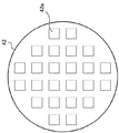
なお、上記実施の形態では、処理室11内に1枚のマイナスイオンソースSが配置される場合を例として示した。このような、マイナスイオンソースSは、例えば7800cm2という大面積を有する。しかし、図3に示すように、大面積のマイナスイオンソースSを用いる代わりに、例えば2500cm2程度の小面積を有する複数のマイナスイオンソースSを並列に並べて使用しても良い。
In the above embodiment, the case where one negative ion source S is arranged in the
また、上記したイオンソース部1の構成は、図1に示した構成に限らず、例えば図4(a)〜4(c)に示すような構成であってもよい。
具体的には、図4(a)に示すように、上記したホットプレート41の代わりに、被覆ヒータ62aを内包する、TaまたはMoから形成される孔開き金属ホットプレート62bが用いられてもよく、温度差を吸収する、中空の金属管63上にホットプレート62bが設置されてもよい。
Further, the configuration of the ion source unit 1 described above is not limited to the configuration illustrated in FIG. 1, and may be configured as illustrated in FIGS. 4A to 4C, for example.
Specifically, as shown in FIG. 4A, a perforated metal hot plate 62b formed of Ta or Mo that encloses the covering
また、図4(b)に示すように、ホットプレート41の代わりに、複数のランプ64を設置し、ランプ64の輻射熱によってマイナスイオンソースSを加熱するようにしてもよい。この場合、接触電極42とランプ64との間には、光を透過する石英窓65が設置される。また、輻射熱をマイナスイオンソースSに集中させるために、ランプ64の光を反射する反射板66等が設置されてもよい。
4B, a plurality of lamps 64 may be installed instead of the
また、図4(c)に示すように、マイクロ波を発生させるマイクロ波電源67と、マイクロ波を伝搬させる導波管68aおよび円錐石英ガラス(導波管)68bと、を設置し、マイクロ波によってマイナスイオンソースSを加熱するようにしてもよい。この場合、円錐石英ガラス68bと接触電極42との間には、マイナスイオンソースSの全面を均一に加熱するために、高いマイクロ波吸収率と高い熱伝導性を有するSiCやムライト(3Al2O3・2SiO2)等から形成される均熱板69を設置しても良い。
Further, as shown in FIG. 4C, a
以上のようにイオンソース部1を構成しても、上記した実施の形態と同様に、マイナスイオンをマイナスイオンソースSから取り出し、半導体ウエハWに注入することができる。 Even if the ion source unit 1 is configured as described above, negative ions can be extracted from the negative ion source S and injected into the semiconductor wafer W, as in the above-described embodiment.
また、ビームライン部2に、イオンビームの進行方向を変化させる偏向装置を設けても良い。この場合、制御装置4は、偏向装置を制御し、半導体ウエハW上の所定領域をイオンビームで走査しても良い。 Further, the beam line unit 2 may be provided with a deflecting device that changes the traveling direction of the ion beam. In this case, the control device 4 may control the deflection device and scan a predetermined region on the semiconductor wafer W with an ion beam.
また、酸素の同位体が、イオンの注入深さ分布に影響を及ぼす場合がある。このような場合は、酸素同位体を排除するための質量分離器を、後段加速器22の前に設置しても良い。この際、イオンソース部1からエンドステーション部3までのビーム路を直線に保つためには、E×B(電場と直交する磁場)タイプの質量分離器を設けると良い。
In addition, oxygen isotopes may affect the ion implantation depth distribution. In such a case, a mass separator for eliminating oxygen isotopes may be installed in front of the
また、12CaO・7Al2O3の品質によっては、O-以外のマイナスイオン(例えばOH-等)が取り出される場合がある。このような場合は、イオンソース部1とビームライン部2との間に質量分離器等を設け、単色化、即ちO-イオンの選別を行ってもよい。 Depending on the quality of 12CaO · 7Al 2 O 3 , negative ions other than O − (for example, OH − ) may be extracted. In such a case, it provided the mass separator or the like between the ion source unit 1 and the beam line section 2, monochromatic, i.e. O - may be carried out selection of ions.
また、上記実施の形態では、マイナスイオンソースSの例として12CaO・7Al2O3を示したが、他のものをマイナスイオンソースSとして用いることもできる。例えば、カルシウムアルミネート(Ca12Al14O33、マイエナイト、アルミン酸カルシウム)、シリコン置換型マイエナイト(Ca12Al10Si4O35)、マイエナイト型ストロンチウムアルミネート(12SrO・7Al2O3、Sr12Al14O33、アルミン酸ストロンチウム)や、上記した接触電極42に使用可能な(1)ジルコニア系の物質、(2)セリア系の物質、(3)ペロブスカイト型(ABO3)複酸化物にドープしたものなどを用いることができる。
In the above embodiment, 12CaO · 7Al 2 O 3 is shown as an example of the negative ion source S, but other negative ion source S can be used. For example, calcium aluminate (Ca 12 Al 14 O 33 , mayenite, calcium aluminate), silicon-substituted mayenite (Ca 12 Al 10 Si 4 O 35 ), mayenite strontium aluminate (12SrO · 7Al 2 O 3 , Sr 12 Al 14 O 33 , strontium aluminate) and (1) zirconia-based materials, (2) ceria-based materials, and (3) perovskite-type (ABO 3 ) complex oxides that can be used for the
1 イオンソース部
2 ビームライン部
3 エンドステーション部
4 制御装置
11 処理室
11a 原料ガス供給管
11b ガス排気管
12 高圧電源
13 原料ガス供給装置
14 ガス排気装置
21 静電レンズ
22 後段加速器
23 四重極レンズ
31 処理室
31a ガス排気管
32 ガス排気装置
41 ホットプレート
42 接触電極
42a 開口
43 クランプ
44 電極支持部材
45 引出電極
46 温度計
47 圧力計
51 基板ホルダ
52 基板加熱ヒータ
53 圧力計
DESCRIPTION OF SYMBOLS 1 Ion source part 2 Beam line part 3 End station part 4
Claims (8)
酸素マイナスイオンラジカルを前記イオンとして、前記被処理基板に注入する、
ことを特徴とするイオン注入装置。 An ion implantation apparatus for forming an oxide layer inside a substrate to be processed by implanting ions into the substrate to be processed,
Injecting oxygen negative ion radicals as the ions into the substrate to be processed;
An ion implantation apparatus characterized by that.
前記イオンのビームを生成するビーム生成手段と、
前記ビーム生成手段が生成する前記ビームを、前記被処理基板上まで真っ直ぐに導いて照射するビーム照射手段と、
から構成される、ことを特徴とする請求項1に記載のイオン注入装置。 The ion implantation apparatus includes:
Beam generating means for generating a beam of the ions;
Beam irradiation means for directing and irradiating the beam generated by the beam generation means up to the substrate to be processed;
The ion implantation apparatus according to claim 1, comprising:
前記ビームを収束する収束レンズと、
前記イオンを加速して所定エネルギーのビームを生成する加速器と、
前記ビームを整形する四重極レンズと、から構成され、
前記収束レンズ、前記加速器、および、前記四重極レンズの中心軸は、一直線に並んでいる、
ことを特徴とする請求項2に記載のイオン注入装置。 The beam irradiation means includes
A converging lens for converging the beam;
An accelerator that accelerates the ions to generate a beam of predetermined energy;
A quadrupole lens for shaping the beam,
The central axes of the converging lens, the accelerator, and the quadrupole lens are aligned.
The ion implantation apparatus according to claim 2.
酸素マイナスイオンラジカルを含有するマイナスイオンソースを加熱する加熱手段と、
前記加熱手段によって加熱される前記マイナスイオンソースに電界を印加し、該マイナスイオンソースに含有されている前記酸素マイナスイオンラジカルを取り出すことにより、前記ビームを生成する電界印加手段と、
から構成されている、ことを特徴とする請求項2または3に記載のイオン注入装置。 The beam generating means includes
A heating means for heating a negative ion source containing oxygen negative ion radicals;
An electric field applying means for generating the beam by applying an electric field to the negative ion source heated by the heating means and taking out the oxygen negative ion radicals contained in the negative ion source;
The ion implantation apparatus according to claim 2, wherein the ion implantation apparatus is configured by:
酸素マイナスイオンラジカルを前記イオンとして、前記被処理基板に注入する工程を備える、
ことを特徴とするイオン注入方法。 An ion implantation method for forming an oxide layer inside a substrate to be processed by implanting ions into the substrate to be processed,
Injecting oxygen negative ion radicals as the ions into the substrate to be processed,
An ion implantation method.
Priority Applications (1)
| Application Number | Priority Date | Filing Date | Title |
|---|---|---|---|
| JP2004107546A JP2005294043A (en) | 2004-03-31 | 2004-03-31 | Ion implantation apparatus and ion implantation method |
Applications Claiming Priority (1)
| Application Number | Priority Date | Filing Date | Title |
|---|---|---|---|
| JP2004107546A JP2005294043A (en) | 2004-03-31 | 2004-03-31 | Ion implantation apparatus and ion implantation method |
Publications (1)
| Publication Number | Publication Date |
|---|---|
| JP2005294043A true JP2005294043A (en) | 2005-10-20 |
Family
ID=35326743
Family Applications (1)
| Application Number | Title | Priority Date | Filing Date |
|---|---|---|---|
| JP2004107546A Pending JP2005294043A (en) | 2004-03-31 | 2004-03-31 | Ion implantation apparatus and ion implantation method |
Country Status (1)
| Country | Link |
|---|---|
| JP (1) | JP2005294043A (en) |
-
2004
- 2004-03-31 JP JP2004107546A patent/JP2005294043A/en active Pending
Similar Documents
| Publication | Publication Date | Title |
|---|---|---|
| JP2010509714A (en) | Apparatus and method for introducing fine particles into semiconductor material using high frequency quadrupole linear accelerator | |
| JPH03163734A (en) | Ion source | |
| CN101802980A (en) | Single wafer implanter for silicon-on-insulator wafer fabrication | |
| CN107039227A (en) | The control method of ion generating means and ion generating means | |
| JP2007525811A (en) | Ion beam current adjustment | |
| JP2011518954A (en) | Deposition system | |
| WO2003067636A1 (en) | Surface treating device and surface treating method | |
| TWI455184B (en) | System and method for reducing pollution and changing surface characteristics by introducing a gas during ion implantation | |
| US7462334B2 (en) | Negatively-charged oxygen atom producing method and producing apparatus | |
| JPH11241888A (en) | Electrostatic floating furnace | |
| JP4147699B2 (en) | Ion implanter | |
| JP2009070886A (en) | Ion injection method and ion injection apparatus | |
| JP2005294043A (en) | Ion implantation apparatus and ion implantation method | |
| KR20140092741A (en) | Ion implantation apparatus and operation method of ion implantation apparatus | |
| CN112802728B (en) | An oxygen ion source based on solid electrolyte, an ion implanter and its application in preparing SOI wafer | |
| JP2010002355A (en) | Metal thin film forming method for microscopic observation sample for scanning electron microscope | |
| JP2010052980A (en) | Oxygen atom generating apparatus | |
| JP2004075431A (en) | Oxygen negative ion generation method and oxygen negative ion generator | |
| JP4253813B2 (en) | Negative ion beam generating apparatus using solid ion conductor, negative ion beam implanting apparatus using solid ion conductor, and space movement propulsion apparatus using solid ion conductor | |
| TWI904562B (en) | Ion implanter and method of operating the ion implanter | |
| JP2009252413A (en) | Electron beam source | |
| JP4114770B2 (en) | Vacuum processing equipment for oxygen ion generation | |
| JP2005294310A (en) | Energy beam irradiation apparatus and pattern making method using the same | |
| JP2002150960A (en) | Ion beam generating apparatus | |
| JP2005294542A (en) | Plasma processing apparatus and plasma processing method |