JP2005294542A - Plasma processing apparatus and plasma processing method - Google Patents
Plasma processing apparatus and plasma processing method Download PDFInfo
- Publication number
- JP2005294542A JP2005294542A JP2004107660A JP2004107660A JP2005294542A JP 2005294542 A JP2005294542 A JP 2005294542A JP 2004107660 A JP2004107660 A JP 2004107660A JP 2004107660 A JP2004107660 A JP 2004107660A JP 2005294542 A JP2005294542 A JP 2005294542A
- Authority
- JP
- Japan
- Prior art keywords
- plasma
- gas
- processing
- processing chamber
- ions
- Prior art date
- Legal status (The legal status is an assumption and is not a legal conclusion. Google has not performed a legal analysis and makes no representation as to the accuracy of the status listed.)
- Pending
Links
Images


Landscapes
- Chemical Vapour Deposition (AREA)
- Drying Of Semiconductors (AREA)
Abstract
【課題】 高真空下であってもプラズマ着火を容易に実現する。
【解決手段】 高圧電源12は、ヒータ33によって加熱されたマイナスイオンソースSからマイナスイオンを取り出す。キャリアガス供給装置15は、キャリアガス(不活性ガス)により、マイナスイオンをプラズマ室21内に供給する。処理ガス供給装置22は、プラズマ処理用の処理ガスをプラズマ室21内に供給し、ガス排気装置23は、プラズマ室21内を高真空に設定する。第1高周波電源25および第2高周波電源27は、下部電極51および上部電極52のそれぞれに高周波を印加し、供給されたマイナスイオンを加速し、供給された処理ガスに衝突させる。これにより、プラズマ室41内にプラズマを発生させ、半導体ウエハWにプラズマ処理を施す。
【選択図】 図2PROBLEM TO BE SOLVED: To easily realize plasma ignition even under a high vacuum.
A high voltage power source 12 takes out negative ions from a negative ion source S heated by a heater 33. The carrier gas supply device 15 supplies negative ions into the plasma chamber 21 by a carrier gas (inert gas). The processing gas supply device 22 supplies a processing gas for plasma processing into the plasma chamber 21, and the gas exhaust device 23 sets the inside of the plasma chamber 21 to a high vacuum. The first high-frequency power source 25 and the second high-frequency power source 27 apply a high frequency to each of the lower electrode 51 and the upper electrode 52, accelerate the supplied negative ions, and collide with the supplied processing gas. Thereby, plasma is generated in the plasma chamber 41 and the semiconductor wafer W is subjected to plasma processing.
[Selection] Figure 2
Description
本発明は、プラズマ処理装置およびプラズマ処理方法に関する。 The present invention relates to a plasma processing apparatus and a plasma processing method.
半導体装置の製造では、半導体ウエハ上に所定の膜を形成したり、半導体ウエハ上に形成された膜をエッチングしたりするために、プラズマを用いる場合がある。 In manufacturing a semiconductor device, plasma may be used to form a predetermined film on a semiconductor wafer or to etch a film formed on the semiconductor wafer.
以上のようなプラズマ処理を実行する場合、処理室内に配置したフィラメントを加熱して熱電子を放出させ、この熱電子を高電圧によって加速し、処理ガスに衝突させることによりプラズマを発生させている(例えば、特許文献1参照。)。
近年、上記プラズマ処理は、高真空下で行われる場合がある。高真空下では、処理室内の処理ガスが希薄であるため、フィラメントから放出される熱電子によってプラズマ着火を行うのが困難である。 In recent years, the plasma treatment may be performed under high vacuum. Under high vacuum, since the processing gas in the processing chamber is dilute, it is difficult to perform plasma ignition with thermionic electrons emitted from the filament.
多量の熱電子を得るためにフィラメントの加熱温度を高く設定すると、フィラメントの寿命が短くなるほか、フィラメント材質の蒸発などによりコンタミネーション、パーティクルが発生するなど、プラズマ処理に対して悪影響が出る。このため、フィラメントの交換等を頻繁に行わなければならない場合がある。また、フィラメント材質は通常金属で、酸化雰囲気では、その高温のため酸化されてしまい使用できない。 If the heating temperature of the filament is set high in order to obtain a large amount of thermoelectrons, the life of the filament is shortened, and contamination and particles are generated due to evaporation of the filament material and the like, which adversely affects the plasma processing. For this reason, it may be necessary to frequently exchange filaments. Also, the filament material is usually a metal, and it cannot be used because it is oxidized in an oxidizing atmosphere due to its high temperature.
また、プラズマ着火を容易にするため、着火時には処理室内の圧力を高めに設定し、プラズマ着火後に処理室内を高真空状態にするという方法も考えられるが、この方法では、圧力調整のための時間が必要となり、所定のプラズマ処理を実行するのに長い時間がかかるという問題がある。 In order to facilitate plasma ignition, a method is also conceivable in which the pressure in the processing chamber is set high during ignition, and the processing chamber is placed in a high vacuum state after plasma ignition. There is a problem that it takes a long time to perform the predetermined plasma processing.
従って、本発明は、コンタミネーションやパーティクルを発生させることなくプラズマ着火を実現するプラズマ処理装置およびプラズマ処理方法を提供することを目的とする。 Accordingly, an object of the present invention is to provide a plasma processing apparatus and a plasma processing method for realizing plasma ignition without generating contamination or particles.
また、本発明は、短時間でプラズマ処理を実行可能なプラズマ処理装置およびプラズマ処理方法を提供することを目的とする。 Another object of the present invention is to provide a plasma processing apparatus and a plasma processing method capable of performing plasma processing in a short time.
上記目的を達成するために、本発明の第1の観点にかかるプラズマ処理装置は、処理室内に配置される半導体ウエハに所定のプラズマ処理を施すプラズマ処理装置であって、前記処理室内に処理ガスを供給するガス供給手段と、前記処理室内にイオンを供給するイオン供給手段と、前記イオン供給手段によって供給される前記イオンを用いて、前記ガス供給手段によって供給される前記処理ガスのプラズマを発生させることにより、前記半導体ウエハに所定のプラズマ処理を施すプラズマ発生手段と、から構成されることを特徴とする。 In order to achieve the above object, a plasma processing apparatus according to a first aspect of the present invention is a plasma processing apparatus that performs a predetermined plasma process on a semiconductor wafer disposed in a processing chamber. A plasma of the processing gas supplied by the gas supply means is generated using a gas supply means for supplying ions, an ion supply means for supplying ions into the processing chamber, and the ions supplied by the ion supply means And plasma generating means for performing a predetermined plasma treatment on the semiconductor wafer.
前記プラズマ発生手段は、前記処理室内に、互いに対向して配置される第1電極および第2電極と、前記第1電極に第1の高周波電圧を印加する第1高周波印加手段と、前記第2電極に第2の高周波電圧を印加する第2高周波印加手段と、前記第1および第2高周波印加手段を制御して前記第1および第2電極に高周波電圧を印加することにより、前記処理室内に供給される前記イオンを加速して該処理室内に供給される前記処理ガスに衝突させ、前記プラズマを発生させる制御手段と、から構成されていてもよい。 The plasma generating means includes a first electrode and a second electrode arranged opposite to each other in the processing chamber, a first high frequency applying means for applying a first high frequency voltage to the first electrode, and the second A second high-frequency applying means for applying a second high-frequency voltage to the electrode, and a high-frequency voltage applied to the first and second electrodes by controlling the first and second high-frequency applying means, thereby allowing the inside of the processing chamber to And control means for accelerating the supplied ions to collide with the processing gas supplied into the processing chamber and generating the plasma.
前記イオン供給手段は、前記イオンとしてマイナスイオンを前記処理室内に供給してもよい。 The ion supply means may supply negative ions as the ions into the processing chamber.
前記イオン供給手段は、前記マイナスイオンを含有するイオンソースを加熱する加熱手段と、前記加熱手段によって加熱される前記イオンソースに電界を印加することにより、該イオンソースに含有されている前記マイナスイオンを取り出す電界印加手段と、から構成されていてもよい。 The ion supply means includes a heating means for heating the ion source containing the negative ions, and the negative ions contained in the ion source by applying an electric field to the ion source heated by the heating means. And an electric field applying means for taking out.
前記加熱手段は、前記マイナスイオンソースを250〜1000℃に加熱してもよい。 The heating means may heat the negative ion source to 250 to 1000 ° C.
上記加熱温度は、好ましくは400〜800℃であり、さらに好ましくは700℃である。 The heating temperature is preferably 400 to 800 ° C, more preferably 700 ° C.
前記電界印加手段は、前記マイナスイオンソースに100〜2000V/cmの電界を印加してもよい。 The electric field applying means may apply an electric field of 100 to 2000 V / cm to the negative ion source.
上記電界の強さは、好ましくは200〜1000V/cmである。 The strength of the electric field is preferably 200 to 1000 V / cm.
前記処理室内のガスを排気することにより、該処理室内の圧力を所定の圧力に設定する排気手段をさらに備え、前記排気手段は、前記処理室内の圧力を0.01Pa以下に設定してもよい。 The apparatus may further comprise exhaust means for setting the pressure in the processing chamber to a predetermined pressure by exhausting the gas in the processing chamber, and the exhaust means may set the pressure in the processing chamber to 0.01 Pa or less. .
本発明の第2の観点にかかるプラズマ処理方法は、処理室内に配置される半導体ウエハに所定のプラズマ処理を施すプラズマ処理方法であって、前記処理室内に処理ガスを供給するガス供給工程と、前記処理室内にイオンを供給するイオン供給工程と、前記イオン供給工程で供給される前記イオンを用いて、前記ガス供給工程で供給される前記処理ガスのプラズマを発生させることにより、前記半導体ウエハに所定のプラズマ処理を施すプラズマ発生工程と、を備えることを特徴とする。 A plasma processing method according to a second aspect of the present invention is a plasma processing method for performing a predetermined plasma processing on a semiconductor wafer disposed in a processing chamber, wherein a gas supply step of supplying a processing gas into the processing chamber; An ion supply step for supplying ions into the processing chamber, and a plasma of the processing gas supplied in the gas supply step is generated using the ions supplied in the ion supply step, whereby the semiconductor wafer is formed. And a plasma generation step of performing a predetermined plasma treatment.
本発明によって、コンタミネーションやパーティクルを発生させることなくプラズマ着火を実現すると共に、短時間でプラズマ処理を実行することができる。 According to the present invention, plasma ignition can be realized without generating contamination and particles, and plasma processing can be executed in a short time.
次に、本発明の実施の形態にかかるプラズマ処理について図面を参照して説明する。 Next, plasma processing according to an embodiment of the present invention will be described with reference to the drawings.
なお、以下では、マイナスイオン、具体的には酸素マイナスイオンラジカル(O-)を用いてプラズマを発生させ、半導体ウエハ上に所定の膜(例えばSiOF膜など)を形成する場合を例にとって説明する。 In the following, a case where a predetermined film (for example, an SiOF film) is formed on a semiconductor wafer by generating plasma using negative ions, specifically, oxygen negative ion radicals (O − ) will be described as an example. .
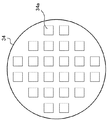
本発明の実施の形態にかかるプラズマ処理を実行するプラズマ処理装置は、例えば図1に示すように、マルチチャンバ型半導体製造装置の一部を構成する。なお、マルチチャンバ型半導体製造装置を構成する処理室の数は、図1に示す数に限定されず、任意である。 A plasma processing apparatus that performs plasma processing according to an embodiment of the present invention constitutes a part of a multi-chamber semiconductor manufacturing apparatus, for example, as shown in FIG. Note that the number of processing chambers constituting the multi-chamber semiconductor manufacturing apparatus is not limited to the number shown in FIG. 1 and is arbitrary.
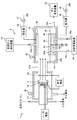
上記プラズマ処理装置は、図2に示すように、マイナスイオンを供給するイオン供給ユニット1と、マイナスイオンを用いてプラズマを発生させ、所定のプラズマ処理を実行するプラズマ処理ユニット2と、イオン供給ユニット1およびプラズマ処理ユニット2を制御する制御装置3と、から構成される。 As shown in FIG. 2, the plasma processing apparatus includes an ion supply unit 1 that supplies negative ions, a plasma processing unit 2 that generates plasma using negative ions, and executes a predetermined plasma process, and an ion supply unit. 1 and a control device 3 for controlling the plasma processing unit 2.
イオン供給ユニット1は、処理室(イオン生成室)11と、高圧電源12と、原料ガス供給装置13と、ガス排気装置14と、キャリアガス供給装置15と、から構成され、マイナスイオンソースSからマイナスイオンを取り出し、プラズマ処理ユニット2に供給する。
The ion supply unit 1 includes a processing chamber (ion generation chamber) 11, a high
なお、マイナスイオンソースSは、例えばC12A7である。マイナスイオンは、C12A7のAlO4四面体が重合して形成するケージ内に閉じこめられている。後述するように、マイナスイオンソースS内のマイナスイオンは、マイナスイオンソースSを所定温度に加熱して所定の強さの電界を印加することによって取り出すことができる。 The negative ion source S is, for example, C12A7. Negative ions are confined in a cage formed by polymerization of C12A7 AlO 4 tetrahedrons. As will be described later, negative ions in the negative ion source S can be extracted by heating the negative ion source S to a predetermined temperature and applying an electric field having a predetermined intensity.
処理室11は、例えばアルミニウム等から形成された処理チャンバである。処理室11の壁には、様々なガスを流通させるための配管が設置されている。
具体的には、マイナスイオンソースSにマイナスイオンを補充するための原料ガスを処理室11内に導入するための原料ガス供給管11aと、処理室11内にキャリアガスを導入するためのキャリアガス供給管11bと、処理室11内のガスを排気するためのガス排気管11cと、取り出されたマイナスイオンをキャリアガスによってプラズマ処理ユニット2に搬送するためのイオン供給管11dと、が設置されている。
The
Specifically, a source gas supply pipe 11a for introducing a source gas for replenishing negative ions into the negative ion source S into the
なお、キャリアガス供給管11bとイオン供給管11dとは、処理室11内に導入されたキャリアガスによるマイナスイオンの搬送がスムーズに行われるように、互いに対向するように設置されている。
The carrier gas supply pipe 11b and the
また、マイナスイオンは、壁にぶつかったり、他の化学種と結びついたりして、その活性を失っていく。このため、イオン供給管11dの内径はできるだけ大きく、長さはできるだけ短く設定される。また、イオン供給管11dの内壁は、マイナスイオンと反応しにくいフルオロカーボン(特にPTFE;四フッ化エチレン樹脂)、または、テフロン(登録商標)等から形成される。さらに、イオン供給管11dは、マイナスイオンを引きつけないように、処理中は、接地されている、または、マイナスの電位に保持されている。
Negative ions collide with walls or bind to other chemical species and lose their activity. For this reason, the inner diameter of the
さらに、マイナスイオンの活性を保つ(再結合を低減する)ため、キャリアガスには、不活性ガス、好ましくは酸素ガスを含有する不活性ガスを用いるのが好ましい。 Further, in order to keep the activity of negative ions (reducing recombination), it is preferable to use an inert gas containing an inert gas, preferably an oxygen gas, as the carrier gas.
また、キャリアガスの流速を高く維持するために、キャリアガスが供給される領域(処理室11内の後述する引出電極36よりも上の領域)は、マイナスイオンが壁等に衝突しない範囲で、できるだけ狭く設定されることが好ましい。
Further, in order to keep the flow rate of the carrier gas high, the region to which the carrier gas is supplied (the region above the
また、処理室11の壁には、処理室11内の温度を測定する温度計31と、処理室11内の圧力を測定する圧力計32と、が設置されている。
処理室11の内部には、ヒータ33と、接触電極34と、電極支持部材35と、引出電極36と、が設置されている。
A
Inside the
ヒータ33は、処理室11内の略中央に設置され、処理室11内に配置されるマイナスイオンソースSを後述する所定温度に加熱する。ヒータ33の内部には、原料ガス供給管11aに接続され、原料ガス供給管11aを介して導入される原料ガスをヒータ33の表面から噴出させるためのガス流路33aが形成されている。
The
接触電極34は、マイナスイオンソースSに貼り付けた状態で製造される。接触電極34は、原料ガスを通す大きさの貫通した空隙のある多孔質とし、原料ガスとマイナスイオンソースSと接触電極34の三相界面を有するように製造する。接触電極34の製造方法としては、例えば、微粉末を膜状に成型し焼結させたもの、もしくはスパッタリングや蒸着によって膜を堆積させる方法がある。
The
また、原料ガスとの接触面積を増やすため、接触電極34は、例えば図3に示すように、複数の開口34aを有する網状に形成してもよい。接触電極34は、電界を印加するための高圧電源12の陰極と電気的に接続されている。原料ガスが接触電極34とヒータ33の隙間から大量に流れ出ることを防ぐため、この間を突起部33bで保持し、気密を保つ。
Further, in order to increase the contact area with the source gas, the
接触電極34に使用可能な物質としては、(1)ジルコニア系の物質、(2)セリア系の物質、(3)ペロブスカイト型(ABO3)複酸化物にドープしたものなどのイオン導電性の高い物質がある。
Materials that can be used for the
上記(1)に該当する物質としては、例えば、YSZ(8mol%Y2O3-ZrO2:イットリア安定化ジルコニア)、SSZ(10mol%Sc2O3-1mol%Al2O3-ZrO2:スカンジア安定化ジルコニア)などが挙げられる。 Examples of the substance corresponding to the above (1) include YSZ (8 mol% Y 2 O 3 —ZrO 2 : yttria stabilized zirconia), SSZ (10 mol% Sc 2 O 3 −1 mol% Al 2 O 3 —ZrO 2 : Scandia-stabilized zirconia).
上記(2)に該当する物質としては、例えばGDC(20mol%GdO1.5-CeO2:ガドリニウム含有セリア)、SDC(20mol%SmO1.5-CeO2:サマリウム含有セリア)などが挙げられる。なお、これら以外に、YO1.5、GaO1.5、NbO2.5などをドープしたものでも良い。 Examples of the substance corresponding to the above (2) include GDC (20 mol% GdO 1.5 -CeO 2 : gadolinium-containing ceria), SDC (20 mol% SmO 1.5 -CeO 2 : samarium-containing ceria) and the like. In addition to these, those doped with YO 1.5 , GaO 1.5 , NbO 2.5, or the like may be used.
上記(3)に該当する物質としては、(La,Sr)MnO3:マンガン酸ランタン−ストロンチウム置換、(La,Sr)(Co,Ni,Fe)O3:コバルト酸ランタン−ストロンチウム置換、ニッケル置換、鉄置換、(La,Sr)(Ga,Mg)O3:ガリウム酸ランタン、ランタンガレート−ストロンチウム置換、マグネシウム置換、(La,Sr)(Cr,Ti,Co)O3:クロム酸ランタン−ストロンチウム置換、チタン置換、コバルト置換、La2/3(Ti0.95Al0.05)O3:チタン酸ランタン−アルミ置換などが挙げられる。なお、ランタンを別のランタノイド(La〜Eu、12配位のイオン半径が比較的大きいもの)(例えば、Sm0.5Sr0.5CoO3など)に置き換えたものでも良い。 Substances corresponding to the above (3) include (La, Sr) MnO 3 : lanthanum manganate-strontium substitution, (La, Sr) (Co, Ni, Fe) O 3 : lanthanum cobaltate-strontium substitution, nickel substitution , Iron substitution, (La, Sr) (Ga, Mg) O 3 : lanthanum gallate, lanthanum gallate-strontium substitution, magnesium substitution, (La, Sr) (Cr, Ti, Co) O 3 : lanthanum chromate-strontium Substitution, titanium substitution, cobalt substitution, La 2/3 (Ti 0.95 Al 0.05 ) O 3 : lanthanum titanate-aluminum substitution and the like. Note that lanthanum may be replaced with another lanthanoid (La to Eu, 12-coordinate ion radius is relatively large) (for example, Sm 0.5 Sr 0.5 CoO 3 or the like).
電極支持部材35は、その一端が処理室11の壁に固定されている。電極支持部材35は、引出電極36を、接触電極34に対向するように支持する。なお、処理室11内の上部には、マイナスイオンを搬送するためのキャリアガスが供給されるので、引出電極36は、キャリアガス供給管11bおよびイオン供給管11dの設置位置よりも低い位置に配置される。
One end of the
引出電極36は、マイナスイオンソースSから取り出されたマイナスイオンが通過可能な形状に形成された電極である。例えば、引出電極36は、網状に形成された金属電極またはセラミック電極あるいはそれらの複合材料で構成される。また、例えば、円板状で中心部に穴を持つ形状でもよい。なお、引出電極36に使用可能な金属としては、耐酸化性を有するPtやAuなどがある。
The
高圧電源12は、その陰極がヒータ33内を通る配線を介して接触電極34に接続され、その陽極が電極支持部材35内を通る配線を介して引出電極36に接続されている。高圧電源12は、接触電極34と引出電極36との間に所定の大きさの電圧を印加することにより、マイナスイオンソースSに、後述する強さの電界を印加する。これにより、所定温度に加熱されたマイナスイオンソースSからマイナスイオンが取り出される。
The high-
原料ガス供給装置13は、原料ガス供給管11aを介して処理室11に接続される。原料ガス供給装置13は、マイナスイオンが取り出されたマイナスイオンソースSに新たなマイナスイオンを補充するための原料ガス(酸素ガス、または、酸素ガスと不活性ガスの混合ガス)を、原料ガス供給管11aを介して処理室11内に供給する。
The source
原料ガス供給装置13によって供給される原料ガスは、原料ガス供給管11aを介してヒータ33の内部に形成されたガス流路33aを通ってヒータ33の表面から噴出される。そして、噴出された原料ガスは、接触電極34を介してマイナスイオンソースSと接触電極34と原料ガスとの三相界面に供給される。
The source gas supplied by the source
また、原料ガス供給装置13は、接触電極34の背面側におけるガスの全圧および原料(酸素)の分圧が、マイナスイオンソースSの引出電極36側におけるガスの全圧および原料の分圧と等しいかまたは少し高くなるように、原料ガスを供給する。この分圧差によりマイナスイオンソースS中の目的イオンの濃度勾配を作り、マイナスイオンを引き出しやすくする。
The source
ガス排気装置14は、排気ポンプ等を備え、ガス排気管11cを介して処理室11に接続される。ガス排気装置14は、処理室11内のガスを排気し、処理室11内の圧力を後述する圧力に設定する。
The
キャリアガス供給装置15は、キャリアガス供給管11bを介して処理室11に接続される。キャリアガス供給装置15は、アルゴン、ヘリウムまたは窒素などの不活性ガスを、マイナスイオンソースSから取り出されたマイナスイオンを搬送するキャリアガスとして処理室11内に供給する。この際、キャリアガス供給装置15は、マイナスイオンが、壁にぶつかったり、他の化学種と結びついたりして、その活性を失うのを抑制するために、比較的高い流速(例えば50cm/s)でキャリアガスを処理室11内に供給する。
The carrier
プラズマ処理ユニット2は、プラズマ室21と、処理ガス供給装置22と、ガス排気装置23と、冷媒循環装置24と、第1高周波電源25と、第1整合器26と、第2高周波電源27と、第2整合器28と、から構成され、所定のプラズマ処理を実行する。
The plasma processing unit 2 includes a
プラズマ室21は、アルマイト処理(陽極酸化処理)されたアルミニウム等の導電性材料から形成された処理チャンバであり、接地されている。プラズマ室21には、下部電極41と、上部電極42と、静電チャック43と、フォーカスリング44と、バッフル板45と、圧力計46と、が設置されている。
The
下部電極41は、例えばアルマイト処理されたアルミニウムから形成され、プラズマ室21内の略中央に設置されている。また、下部電極41は、その内部に、半導体ウエハWの温度を所定温度に維持するための冷媒が流通する空洞41aを有する。空洞41aは、例えば環状に、形成されている。
The
上部電極42は、例えばアルマイト処理されたアルミニウムから形成され、下部電極41に対向するように設置されている。上部電極42は、中空構造となっており、その下面には、処理ガスおよびマイナスイオンを吹き出すための1以上のガス孔が形成されている。
The
静電チャック43は、半導体ウエハWと同等の平面サイズを有し、下部電極41上に設置されている。静電チャック43は、直流電源43aを有し、載置される半導体ウエハWを固定する。
The
フォーカスリング44は、静電チャック43、即ち載置された半導体ウエハW、を囲むように、下部電極41上に設置されている。フォーカスリング44は、プラズマによって発生した反応性イオン等を引き寄せない絶縁性の材質、例えば石英、から形成されている。このフォーカスリング44によって、プラズマ室21内で発生したプラズマを、半導体ウエハWに効果的に入射させることができる。
The
バッフル板45は、複数の微細な細孔を有し、下部電極41を取り囲んで、プラズマ室21内を上下の2つの領域に分断するように設置されている。バッフル板45は、プラズマ室21内で発生したプラズマが、排ガスと一緒にプラズマ室21から排出されるのを防止すると共に、排気流の流れを整えて、排ガスを均一に排出するために設けられている。
The
なお、バッフル板45が有する細孔の幅は、プラズマの通過が不可能であり、排ガスの通過が可能な幅、例えば0.8〜1mm程度に設定されている。
圧力計46は、プラズマ室21内の圧力を測定するために設置されている。
In addition, the width | variety of the pore which the
The
処理ガス供給装置22は、処理ガス供給管22aを介して上部電極42に接続されている。処理ガス供給装置22は、プラズマ処理に使用される所定の処理ガスを所定の流量でプラズマ室21内に供給する。処理ガス供給装置22が供給する処理ガスは、上部電極42が有するガス孔を介してプラズマ室21内に供給される。
The processing
なお、上記したイオン供給管11dは、処理ガス供給管22aに接続されている。従って、イオン供給ユニット1が供給するマイナスイオンは、処理ガスと共に、上部電極42が有するガス孔を介してプラズマ室21内に供給される。
The above-described
処理ガス供給装置22が供給する処理ガスは、半導体ウエハW上に形成される膜の種類に応じて決定される。例えば、形成対象の膜がSiOF膜である場合、SiF4、SiH4、O2、NF3、NH3のガスと、Arガスとの混合ガスが処理ガスとして供給される。
The processing gas supplied by the processing
ガス排気装置23は、ガス排気管23aを介してプラズマ室21に接続される。なお、ガス排気管23aは、バッフル板45よりも下の位置で、プラズマ室21に接続されている。ガス排気装置23は、排気ポンプ等を備え、プラズマ室21内のガスを排気し、プラズマ室21内を所定の圧力(例えば0.01Pa以下)に設定する。
The
冷媒循環装置24は、冷媒供給管24aを介して、下部電極41内の空洞41aに接続されている。冷媒循環装置24は、所定温度の冷媒を空洞41a内に循環させる。これにより、冷媒循環装置24は、静電チャック43上に載置された半導体ウエハWの温度を所定温度に維持する。
なお、冷媒循環装置24が循環させる冷媒は、例えばフロリナートであり、その温度は、例えば50℃に設定される。
The
In addition, the refrigerant | coolant which the refrigerant |
第1高周波電源25は、第1整合器26を介して、下部電極41に接続されている。第1高周波電源25は、下部電極41に所定の高周波電圧(例えば0.1〜13MHz)を印加する。
The first high
第2高周波電源27は、第2整合器28を介して、上部電極42に接続されている。第2高周波電源27は、上部電極42に所定の高周波電圧(例えば13〜150MHz)を印加する。
The second high
制御装置3は、マイクロコンピュータ等から構成され、所定のプラズマ処理を実行するためのプログラムを記憶している。制御装置3は、記憶しているプログラムに従ってイオン供給ユニット1の動作を制御し、マイナスイオンを供給させる。また、制御装置3は、記憶しているプログラムに従って、プラズマ処理ユニット2の動作を制御し、半導体ウエハW上に所定の膜を形成する。なお、制御装置3の詳しい動作については後述する。 The control device 3 is composed of a microcomputer or the like, and stores a program for executing predetermined plasma processing. The control device 3 controls the operation of the ion supply unit 1 according to the stored program and supplies negative ions. Further, the control device 3 controls the operation of the plasma processing unit 2 according to the stored program, and forms a predetermined film on the semiconductor wafer W. The detailed operation of the control device 3 will be described later.
次に、ヒータ33が加熱するマイナスイオンソースSの温度、高圧電源12が印加する電圧の大きさ、および、ガス排気装置14が設定する処理室11内の圧力の大きさについて説明する。
Next, the temperature of the negative ion source S heated by the
マイナスイオンソースS内のマイナスイオンは、マイナスイオンソースSを加熱して電界を印加することにより取り出される。この際、マイナスイオンソースSの温度が低すぎると、マイナスイオンソースS中のマイナスイオンが活性化しないため、マイナスイオンを取り出すのが困難になる。一方、マイナスイオンソースSの温度が高すぎると、活性化されたマイナスイオンが異常発生し、マイナスイオンソースSが変性するおそれがある。さらに、加熱温度が高すぎると、処理室11内に設置されるヒータ33や電極などに、高い耐熱性を有する特殊なセラミックや金属等を用いなければならなくなる。
Negative ions in the negative ion source S are taken out by heating the negative ion source S and applying an electric field. At this time, if the temperature of the negative ion source S is too low, the negative ions in the negative ion source S are not activated, making it difficult to extract the negative ions. On the other hand, if the temperature of the negative ion source S is too high, activated negative ions may be abnormally generated and the negative ion source S may be denatured. Further, if the heating temperature is too high, a special ceramic or metal having high heat resistance must be used for the
このため、ヒータ33が加熱するマイナスイオンソースSの温度は、マイナスイオンソースSからマイナスイオンを容易に取り出すことが可能であり、一般的な金属などの材質を使用可能な温度、250〜1000℃、好ましくは400〜800℃、さらに好ましくは700℃に設定される。
For this reason, the temperature of the negative ion source S heated by the
以上のような好適な温度に加熱されたマイナスイオンソースSに電界を印加することにより、マイナスイオンソースSに含有されているマイナスイオンを取り出すことができる。 By applying an electric field to the negative ion source S heated to a suitable temperature as described above, negative ions contained in the negative ion source S can be taken out.
この際、印加される電界が弱すぎると、プラズマ生成に必要な量のマイナスイオンを取り出すことができず、一方、強すぎると、必要以上のマイナスイオンが取り出される。 At this time, if the applied electric field is too weak, an amount of negative ions necessary for plasma generation cannot be extracted. On the other hand, if it is too strong, more negative ions than necessary are extracted.
必要以上のマイナスイオンが取り出された場合、目的以外の部分(処理室11の内壁および引出電極36等)において生じるマイナスイオンとの反応が、プラズマ処理に影響を与える場合がある。このため、マイナスイオンソースSに印加する電界の強さは、必要なマイナスイオンの量(電流量)を得ることができる強さに設定される。
When more negative ions than necessary are taken out, the reaction with negative ions generated in portions other than the target (the inner wall of the
例えば、0.01Pa程度(0.075〜0.10mTorr)の圧力下でプラズマを生成するためには、プラズマ発生領域内にある気体分子の10%のマイナスイオン量が必要である。また、0.1Pa程度(0.75〜1.0mTorr)の圧力下でプラズマを生成するためには、プラズマ発生領域内にある気体分子の0.1%のマイナスイオン量が必要である。 For example, in order to generate plasma under a pressure of about 0.01 Pa (0.075 to 0.10 mTorr), a negative ion amount of 10% of gas molecules in the plasma generation region is required. Further, in order to generate plasma under a pressure of about 0.1 Pa (0.75 to 1.0 mTorr), a negative ion amount of 0.1% of gas molecules in the plasma generation region is required.
プラズマ発生領域の体積が約700cm3(φ300mm、高さ10mm)であると仮定すると、圧力が0.01Pa程度に設定されている場合、イオン電流を10μAとすることにより、3秒間で気体分子の10%のマイナスイオンを供給することができる。また、圧力が0.1Pa程度に設定されている場合、イオン電流を1μAとすることにより、3秒間で気体分子の0.1%のマイナスイオンを供給することができる。 Assuming that the volume of the plasma generation region is about 700 cm 3 (φ300 mm, height 10 mm), when the pressure is set to about 0.01 Pa, the ion current is set to 10 μA, and the gas molecules 10% negative ions can be supplied. When the pressure is set to about 0.1 Pa, negative ions of 0.1% of gas molecules can be supplied in 3 seconds by setting the ion current to 1 μA.
マイナスイオンソースSから得られる電流量は、マイナスイオンソースSのサイズ(イオンが取り出される面の面積)が大きくなるほど大きく、また、印加する電界を強くするほど大きくなる。 The amount of current obtained from the negative ion source S increases as the size of the negative ion source S (area of the surface from which ions are extracted) increases and increases as the applied electric field increases.
例えば、イオンが取り出される面の面積が10cm2であるC12A7をマイナスイオンソースSとして用い、マイナスイオンソースSを700℃に加熱した場合、400V/cmの電界を印加することにより、10μAの電流量を得ることができる。 For example, when C12A7 whose area from which ions are extracted is 10 cm 2 is used as the negative ion source S and the negative ion source S is heated to 700 ° C., an electric current of 10 μA is applied by applying an electric field of 400 V / cm. Can be obtained.
このように、マイナスイオンソースSに印加される電界の強さ(即ち、高圧電源12が印加する電圧の大きさ)は、マイナスイオンソースSのサイズに応じて、上記した電流量が得られるように設定される。 Thus, the intensity of the electric field applied to the negative ion source S (that is, the magnitude of the voltage applied by the high-voltage power supply 12) can be obtained by the amount of current described above according to the size of the negative ion source S. Set to
ただし、印加する電界の大きさが100V/cm未満では、マイナスイオンソースSからマイナスイオンを取り出すことができない場合があり、また、2000V/cm以上では、異常放電が生じる。このため、高圧電源12が印加する電圧の大きさは、印加する電界の大きさが100〜2000V/cm、好ましくは200〜1000V/cmの範囲内に収まるように設定される。
However, when the magnitude of the applied electric field is less than 100 V / cm, negative ions may not be extracted from the negative ion source S, and when 2000 V / cm or more, abnormal discharge occurs. For this reason, the magnitude of the voltage applied by the high-
マイナスイオンソースSから取り出されたマイナスイオンは、処理室11からイオン供給管11dおよび処理ガス供給管22aを介してプラズマ室21に供給される。この際、処理室11内の圧力がプラズマ室21内の圧力よりも低いと、逆方向(プラズマ室21から処理室11への方向)の拡散が起こり、マイナスイオンを供給しにくくなる。
Negative ions extracted from the negative ion source S are supplied from the
このため、ガス排気装置14は、マイナスイオンが処理室11からプラズマ室21に円滑に供給されるように、処理室11内の圧力を、プラズマ室21の圧力以上(具体的には、1〜10倍)に設定する。
例えば、プラズマ室21の圧力が0.01Paに設定される場合、ガス排気装置14は、処理室11内の圧力を、0.01〜0.1Paに設定する。
For this reason, the
For example, when the pressure in the
次に、上記したプラズマ処理装置の動作について説明する。
マイナスイオンソースSは、処理室11内に予めセットされている。半導体ウエハWは、例えばマルチチャンバ型半導体製造装置の搬送アームによって、プラズマ室21の図示せぬ搬送口から静電チャック43上に載置される。
Next, the operation of the above plasma processing apparatus will be described.
The negative ion source S is set in the
静電チャック43上に半導体ウエハWが載置されると、制御装置3は、静電チャック43を制御して載置された半導体ウエハWを固定し、予め記憶しているプログラムに従って、イオン供給ユニット1およびプラズマ処理ユニット2の動作を制御し、以下に示すプラズマ処理を行う。
When the semiconductor wafer W is placed on the
初めに、制御装置3は、原料ガス供給装置13を制御し、処理室11内に原料ガスを供給すると共に、ガス排気装置14を制御し、圧力計32の測定結果を用いて、処理室11内の圧力を所定の圧力(例えば0.1Pa)に設定する。
First, the control device 3 controls the raw material
この際、制御装置3は、接触電極34の背面側におけるガスの全圧、および原料の分圧が、マイナスイオンソースSの引出電極36側における雰囲気の全圧、および原料の分圧よりも高くなるように原料ガスを供給する。
At this time, the control device 3 determines that the total pressure of the gas on the back side of the
そして、制御装置3は、ヒータ33を制御し、温度計31の測定結果を用いて、接触電極34上に載置されたマイナスイオンソースSを約700℃に加熱する。
続いて、制御装置3は、キャリアガス供給装置15を制御し、処理室11内に所定の流量でキャリアガスを供給する。
Then, the control device 3 controls the
Subsequently, the control device 3 controls the carrier
その後、制御装置3は、高圧電源12を制御して、接触電極34と引出電極36との間に電圧を印加することにより、上記した強さの電界をマイナスイオンソースSに印加する。
Thereafter, the control device 3 controls the high-
これにより、マイナスイオンソースS内のマイナスイオンが印加された電界によって取り出される。取り出されたマイナスイオンは、引出電極36を通過し、処理室11内の上部を流通するキャリアガス(不活性ガス)によって、プラズマ処理ユニット2に搬送される。
Thereby, the negative ions in the negative ion source S are taken out by the applied electric field. The extracted negative ions pass through the
また、制御装置3は、静電チャック43上に半導体ウエハWを固定した後、処理ガス供給装置22を制御して、処理ガスをプラズマ室21内に導入する。
そして、制御装置3は、圧力計46による測定結果を用い、ガス排気装置23を制御して、プラズマ室21内の圧力を所定圧力(例えば0.01Pa)に設定する。
Further, after fixing the semiconductor wafer W on the
And the control apparatus 3 controls the
また、制御装置3は、冷媒循環装置24を制御して、下部電極41内の空洞41aに所定温度の冷媒を循環させ、半導体ウエハWの温度を所定温度に設定する。
プラズマ室21内の圧力が所定圧力になると、制御装置3は、第1高周波電源25、第1整合器26、第2高周波電源27および第2整合器28を制御して、下部電極41および上部電極42のそれぞれに所定の高周波を印加する。これにより、供給されたマイナスイオンが加速される。
Further, the control device 3 controls the
When the pressure in the
この際、マイナスイオンは、プラズマ着火に適した密度(または量)で供給されているので、プラズマ室21内が高真空に設定されていても、マイナスイオンは供給された処理ガスに容易に衝突する。これにより、プラズマ室21内に、プラズマを容易に発生させることができる。
At this time, since the negative ions are supplied at a density (or amount) suitable for plasma ignition, even if the inside of the
以上のように、マイナスイオンの密度(または量)は、マイナスイオンソースSに印加する電界によって容易に制御することができる。このように、容易に高密度を実現可能なマイナスイオンを用いることにより、高真空下であっても、容易にプラズマ着火を行うことができる。これにより、所定のプラズマ処理が速やかに開始され、半導体装置の製造にかかる時間を節約することができる。また、原料ガスに含まれる元素と同じ元素のイオンを用いることにより、コンタミネーションやパーティクルを生成せずにプラズマ着火を行うことができる。 As described above, the density (or amount) of negative ions can be easily controlled by the electric field applied to the negative ion source S. Thus, by using negative ions that can easily achieve high density, plasma ignition can be easily performed even under high vacuum. Thereby, the predetermined plasma processing is started quickly, and the time required for manufacturing the semiconductor device can be saved. Further, by using ions of the same element as the element contained in the source gas, plasma ignition can be performed without generating contamination or particles.
実際に、プラズマ室21内の圧力を0.1Paに設定し、イオン電流1μAでマイナスイオンを3秒間供給した後に、100MHzの高周波を印加することによりプラズマを生成することができた。また、さらに低い0.01Paに圧力を設定した場合でも、イオン電流10μAでマイナスイオンを3秒間供給した後に、100MHzの高周波を印加することによりプラズマを生成することができた。また、圧力を0.8Paに設定した場合でも、イオン電流1μAでマイナスイオンを供給し、60MHzの高周波を印加することによりプラズマを生成することができた。
以上のように、通常ではプラズマ着火が困難な条件であっても、マイナスイオンを利用することにより、容易にプラズマを生成することができた。
Actually, it was possible to generate plasma by setting the pressure in the
As described above, it was possible to easily generate plasma by using negative ions even under conditions where plasma ignition was difficult.
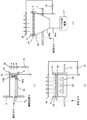
なお、上記したイオン供給ユニット1の構成は、図2に示した構成に限らず、例えば図4(a)〜4(c)に示すような構成であってもよい。
具体的には、マイナスイオンソースSが円盤状である場合、クランプ61によってマイナスイオンソースSを固定してもよい。この場合は、例えば図4(a)に示すように、マイナスイオンソースSを垂直に設置することも可能である。
The configuration of the above-described ion supply unit 1 is not limited to the configuration illustrated in FIG. 2, and may be configured as illustrated in FIGS. 4A to 4C, for example.
Specifically, when the negative ion source S has a disk shape, the negative ion source S may be fixed by the
また、図4(a)に示すように、ヒータ33の代わりに、被覆ヒータ62aを内包する、TaまたはMoから形成される孔開き金属ホットプレート62bが用いられてもよく、温度差を吸収する、中空の金属管63上にホットプレート62bが設置されてもよい。
Further, as shown in FIG. 4A, a perforated metal hot plate 62b formed of Ta or Mo containing a
また、図4(b)に示すように、ヒータ33の代わりに、複数のランプ64を設置し、ランプ64の輻射熱によってマイナスイオンソースSを加熱するようにしてもよい。この場合、接触電極34とランプ64との間には、光を透過する石英窓65が設置される。また、輻射熱をマイナスイオンソースSに集中させるために、ランプ64の光を反射する反射板66等が設置されてもよい。
In addition, as shown in FIG. 4B, a plurality of
また、図4(c)に示すように、マイクロ波を発生させるマイクロ波電源67と、マイクロ波を伝搬させる導波管68aおよび円錐石英ガラス(導波管)68bと、を設置し、マイクロ波によってマイナスイオンソースSを加熱するようにしてもよい。この場合、円錐石英ガラス68bと接触電極34との間には、マイナスイオンソースSの全面を均一に加熱するために、高いマイクロ波吸収率と高い熱伝導性を有するSiCやムライト(3Al2O3・2SiO2)等から形成される均熱板69を設置しても良い。
Further, as shown in FIG. 4C, a
以上のようにイオン供給ユニット1を構成しても、上記した実施の形態と同様に、マイナスイオンをマイナスイオンソースSから取り出し、プラズマの生成に用いることができる。 Even if the ion supply unit 1 is configured as described above, negative ions can be extracted from the negative ion source S and used to generate plasma, as in the above-described embodiment.
また、上記したイオン供給ユニット1は、図4(a)に示したように構成され、図5に示すように、マイナスイオンソースSから取り出されたマイナスイオンが、プラズマ室21内のプラズマ生成領域に直接供給されるようにしても良い。言い換えると、接触電極34と引出電極36との間の電位差により加速されたマイナスイオンが、そのまま真っ直ぐ進んでプラズマ生成領域に供給されるように、処理室11とプラズマ室21とをイオン供給管11dで接続しても良い。このようにすれば、キャリアガスを用いずに、マイナスイオンをプラズマ室21内に供給することができる。
Further, the above-described ion supply unit 1 is configured as shown in FIG. 4A, and as shown in FIG. 5, the negative ions extracted from the negative ion source S are generated in the plasma generation region in the
また、上記実施の形態では、マイナスイオンソースSの例としてC12A7を示したが、他のものをマイナスイオンソースSとして用いることもできる。例えば、カルシウムアルミネート(Ca12Al14O33、マイエナイト、アルミン酸カルシウム)、シリコン置換型マイエナイト(Ca12Al10Si4O35)、マイエナイト型ストロンチウムアルミネート(12SrO・7Al2O3、Sr12Al14O33、アルミン酸ストロンチウム)や、上記した接触電極34に使用可能な(1)ジルコニア系の物質、(2)セリア系の物質、(3)ペロブスカイト型(ABO3)複酸化物にドープしたものなどを用いることができる。
In the above embodiment, C12A7 is shown as an example of the negative ion source S, but other negative ion source S can be used. For example, calcium aluminate (Ca 12 Al 14 O 33 , mayenite, calcium aluminate), silicon-substituted mayenite (Ca 12 Al 10 Si 4 O 35 ), mayenite strontium aluminate (12SrO · 7Al 2 O 3 , Sr 12 Al 14 O 33 , strontium aluminate) and (1) zirconia-based materials, (2) ceria-based materials, (3) perovskite (ABO 3 ) double oxides that can be used for the
また、上記実施の形態では、酸素マイナスイオンラジカルを用いてプラズマを発生させる場合を例として示したが、他のイオンを用いてプラズマを発生させても良い。例えば、OH-、F-、Cl-等のイオンを用いても良い。 In the above-described embodiment, the case where plasma is generated using oxygen negative ion radicals is shown as an example, but plasma may be generated using other ions. For example, ions such as OH − , F − and Cl − may be used.
また、上記実施の形態では、形成対象膜の例としてSiOF膜を示したが、形成対象の膜は、SiO2、SiN、SiC、SiCOH、CFなど、プラズマ処理によって形成可能なものであれば何でも良い。 In the above embodiment, the SiOF film is shown as an example of the film to be formed. However, any film that can be formed by plasma processing, such as SiO 2 , SiN, SiC, SiCOH, or CF, can be used. good.
また、上記実施の形態では、半導体ウエハW上に所定の膜を形成する場合を例にとって説明したが、上記プラズマ処理装置は、他のプラズマ処理にも適用可能である。例えば、半導体ウエハW上に形成された膜をプラズマエッチングする場合等にも適用することができる。 In the above embodiment, the case where a predetermined film is formed on the semiconductor wafer W has been described as an example. However, the plasma processing apparatus can also be applied to other plasma processing. For example, the present invention can be applied to a case where a film formed on the semiconductor wafer W is subjected to plasma etching.
また、上記したイオン供給ユニット1の代わりにプラズマ発生装置を用い、例えばBF3、PH3、AsH3等のガスをアーク放電によってイオン化し、これによって得られるマイナスイオンまたはプラスイオンをプラズマ室21内に供給して、上記と同様に、プラズマを発生させても良い。
Further, instead of the ion supply unit 1 described above, a plasma generator is used, for example, gas such as BF 3 , PH 3 , AsH 3 is ionized by arc discharge, and negative ions or positive ions obtained thereby are converted into the
1 イオン供給ユニット
2 プラズマ処理ユニット
3 制御装置
11 処理室
11a 原料ガス供給管
11b キャリアガス供給管
11c ガス排気管
11d イオン供給管
12 高圧電源
13 原料ガス供給装置
14 ガス排気装置
15 キャリアガス供給装置
21 プラズマ室
22 処理ガス供給装置
22a 処理ガス供給管
23 ガス排気装置
23a ガス排気管
24 冷媒循環装置
24a 冷媒供給管
25 第1高周波電源
26 第1整合器
27 第2高周波電源
28 第2整合器
31 温度計
32 圧力計
33 ヒータ
33a ガス流路
33b 突起部
34 接触電極
35 電極支持部材
36 引出電極
41 下部電極
41a 空洞
42 上部電極
43 静電チャック
43a 直流電源
44 フォーカスリング
45 バッフル板
46 圧力計
DESCRIPTION OF SYMBOLS 1 Ion supply unit 2 Plasma processing unit 3
Claims (8)
前記処理室内に処理ガスを供給するガス供給手段と、
前記処理室内にイオンを供給するイオン供給手段と、
前記イオン供給手段によって供給される前記イオンを用いて、前記ガス供給手段によって供給される前記処理ガスのプラズマを発生させることにより、前記半導体ウエハに所定のプラズマ処理を施すプラズマ発生手段と、
から構成されることを特徴とするプラズマ処理装置。 A plasma processing apparatus for performing predetermined plasma processing on a semiconductor wafer disposed in a processing chamber,
Gas supply means for supplying a processing gas into the processing chamber;
Ion supply means for supplying ions into the processing chamber;
Plasma generating means for performing a predetermined plasma treatment on the semiconductor wafer by generating plasma of the processing gas supplied by the gas supply means using the ions supplied by the ion supply means;
A plasma processing apparatus comprising:
前記処理室内に、互いに対向して配置される第1電極および第2電極と、
前記第1電極に第1の高周波電圧を印加する第1高周波印加手段と、
前記第2電極に第2の高周波電圧を印加する第2高周波印加手段と、
前記第1および第2高周波印加手段を制御して前記第1および第2電極に高周波電圧を印加することにより、前記処理室内に供給される前記イオンを加速して該処理室内に供給される前記処理ガスに衝突させ、前記プラズマを発生させる制御手段と、
から構成されている、ことを特徴とする請求項1に記載のプラズマ処理装置。 The plasma generating means includes
A first electrode and a second electrode disposed opposite to each other in the processing chamber;
First high frequency applying means for applying a first high frequency voltage to the first electrode;
Second high frequency applying means for applying a second high frequency voltage to the second electrode;
The first and second high-frequency applying means are controlled to apply a high-frequency voltage to the first and second electrodes, thereby accelerating the ions supplied into the processing chamber and supplying the ions into the processing chamber. Control means for colliding with a processing gas and generating the plasma;
The plasma processing apparatus according to claim 1, comprising:
前記マイナスイオンを含有するイオンソースを加熱する加熱手段と、
前記加熱手段によって加熱される前記イオンソースに電界を印加することにより、該イオンソースに含有されている前記マイナスイオンを取り出す電界印加手段と、
から構成されている、ことを特徴とする請求項3に記載のプラズマ処理装置。 The ion supply means includes
Heating means for heating the ion source containing the negative ions;
An electric field applying means for taking out the negative ions contained in the ion source by applying an electric field to the ion source heated by the heating means;
The plasma processing apparatus according to claim 3, comprising:
前記排気手段は、前記処理室内の圧力を0.01Pa以下に設定する、
ことを特徴とする請求項1乃至6の何れか1項に記載のプラズマ処理装置。 An exhaust means for setting the pressure in the processing chamber to a predetermined pressure by exhausting the gas in the processing chamber;
The exhaust means sets the pressure in the processing chamber to 0.01 Pa or less;
The plasma processing apparatus according to any one of claims 1 to 6, wherein:
前記処理室内に処理ガスを供給するガス供給工程と、
前記処理室内にイオンを供給するイオン供給工程と、
前記イオン供給工程で供給される前記イオンを用いて、前記ガス供給工程で供給される前記処理ガスのプラズマを発生させることにより、前記半導体ウエハに所定のプラズマ処理を施すプラズマ発生工程と、
を備えることを特徴とするプラズマ処理方法。 A plasma processing method for performing predetermined plasma processing on a semiconductor wafer disposed in a processing chamber,
A gas supply step of supplying a processing gas into the processing chamber;
An ion supply step for supplying ions into the processing chamber;
Generating a plasma of the processing gas supplied in the gas supply step using the ions supplied in the ion supply step, thereby performing a predetermined plasma treatment on the semiconductor wafer; and
A plasma processing method comprising:
Priority Applications (1)
| Application Number | Priority Date | Filing Date | Title |
|---|---|---|---|
| JP2004107660A JP2005294542A (en) | 2004-03-31 | 2004-03-31 | Plasma processing apparatus and plasma processing method |
Applications Claiming Priority (1)
| Application Number | Priority Date | Filing Date | Title |
|---|---|---|---|
| JP2004107660A JP2005294542A (en) | 2004-03-31 | 2004-03-31 | Plasma processing apparatus and plasma processing method |
Publications (1)
| Publication Number | Publication Date |
|---|---|
| JP2005294542A true JP2005294542A (en) | 2005-10-20 |
Family
ID=35327134
Family Applications (1)
| Application Number | Title | Priority Date | Filing Date |
|---|---|---|---|
| JP2004107660A Pending JP2005294542A (en) | 2004-03-31 | 2004-03-31 | Plasma processing apparatus and plasma processing method |
Country Status (1)
| Country | Link |
|---|---|
| JP (1) | JP2005294542A (en) |
-
2004
- 2004-03-31 JP JP2004107660A patent/JP2005294542A/en active Pending
Similar Documents
| Publication | Publication Date | Title |
|---|---|---|
| US11404281B2 (en) | Method of etching silicon containing films selectively against each other | |
| CN110049614B (en) | Microwave plasma device and plasma excitation method | |
| EP0874386B1 (en) | Apparatus and process for remote microwave plasma generation | |
| CN102160141B (en) | Apparatus and method for producing dielectric layers with microwave plasma | |
| TWI425883B (en) | Plasma processing device | |
| WO2003096400A1 (en) | Plasma processing equipment and plasma processing method | |
| WO2011021539A1 (en) | Plasma treatment device and plasma treatment method | |
| JP2020517106A (en) | Optical emission spectroscopy (OES) for remote plasma monitoring | |
| US20200144031A1 (en) | Etching method and plasma processing apparatus | |
| JP2009206341A (en) | Microwave plasma processing apparatus, dielectric window member used therefor, and manufacturing method of dielectric window member | |
| US6765216B2 (en) | Method and apparatus for producing atomic flows of molecular gases | |
| US7462334B2 (en) | Negatively-charged oxygen atom producing method and producing apparatus | |
| TW200903636A (en) | Plasma processing equipment and method for processing plasma | |
| JP2005294542A (en) | Plasma processing apparatus and plasma processing method | |
| JP4983091B2 (en) | Method for forming electrolyte membrane, film forming apparatus, and solid fuel cell | |
| JPWO1996017803A1 (en) | Method and apparatus for generating negatively charged oxygen atoms | |
| US20070131539A1 (en) | Combination heater/generator for generating negatively charged oxygen atoms | |
| JP2004075431A (en) | Oxygen negative ion generation method and oxygen negative ion generator | |
| CN109905955B (en) | Atomic plasma formation device and its application | |
| JP2005150632A (en) | Reduction device and reduction method | |
| JPH08222553A (en) | Processing device and processing method | |
| JP2005302801A (en) | Cleaning device and cleaning method | |
| CN116988020B (en) | Atmosphere control device for electron beam evaporation source, coating equipment and coating process | |
| JP2005294043A (en) | Ion implantation apparatus and ion implantation method | |
| JP2010052980A (en) | Oxygen atom generating apparatus |