JP2005294034A - Connector - Google Patents
Connector Download PDFInfo
- Publication number
- JP2005294034A JP2005294034A JP2004107303A JP2004107303A JP2005294034A JP 2005294034 A JP2005294034 A JP 2005294034A JP 2004107303 A JP2004107303 A JP 2004107303A JP 2004107303 A JP2004107303 A JP 2004107303A JP 2005294034 A JP2005294034 A JP 2005294034A
- Authority
- JP
- Japan
- Prior art keywords
- header
- contact
- socket
- contacts
- connector
- Prior art date
- Legal status (The legal status is an assumption and is not a legal conclusion. Google has not performed a legal analysis and makes no representation as to the accuracy of the status listed.)
- Pending
Links
- 238000003780 insertion Methods 0.000 claims abstract description 39
- 230000037431 insertion Effects 0.000 claims abstract description 39
- 238000000605 extraction Methods 0.000 claims description 4
- 230000002093 peripheral effect Effects 0.000 abstract description 21
- 238000005452 bending Methods 0.000 description 6
- 238000000465 moulding Methods 0.000 description 6
- 239000011347 resin Substances 0.000 description 6
- 229920005989 resin Polymers 0.000 description 6
- 239000002184 metal Substances 0.000 description 4
- 239000007769 metal material Substances 0.000 description 4
- 230000003014 reinforcing effect Effects 0.000 description 4
- 238000000034 method Methods 0.000 description 3
- 238000005192 partition Methods 0.000 description 2
- 238000005476 soldering Methods 0.000 description 2
- 238000013459 approach Methods 0.000 description 1
- 230000000694 effects Effects 0.000 description 1
- 238000009413 insulation Methods 0.000 description 1
- 230000002787 reinforcement Effects 0.000 description 1
- 239000000758 substrate Substances 0.000 description 1
Images

Classifications
-
- H—ELECTRICITY
- H01—ELECTRIC ELEMENTS
- H01R—ELECTRICALLY-CONDUCTIVE CONNECTIONS; STRUCTURAL ASSOCIATIONS OF A PLURALITY OF MUTUALLY-INSULATED ELECTRICAL CONNECTING ELEMENTS; COUPLING DEVICES; CURRENT COLLECTORS
- H01R12/00—Structural associations of a plurality of mutually-insulated electrical connecting elements, specially adapted for printed circuits, e.g. printed circuit boards [PCB], flat or ribbon cables, or like generally planar structures, e.g. terminal strips, terminal blocks; Coupling devices specially adapted for printed circuits, flat or ribbon cables, or like generally planar structures; Terminals specially adapted for contact with, or insertion into, printed circuits, flat or ribbon cables, or like generally planar structures
- H01R12/70—Coupling devices
- H01R12/71—Coupling devices for rigid printing circuits or like structures
-
- H—ELECTRICITY
- H01—ELECTRIC ELEMENTS
- H01R—ELECTRICALLY-CONDUCTIVE CONNECTIONS; STRUCTURAL ASSOCIATIONS OF A PLURALITY OF MUTUALLY-INSULATED ELECTRICAL CONNECTING ELEMENTS; COUPLING DEVICES; CURRENT COLLECTORS
- H01R12/00—Structural associations of a plurality of mutually-insulated electrical connecting elements, specially adapted for printed circuits, e.g. printed circuit boards [PCB], flat or ribbon cables, or like generally planar structures, e.g. terminal strips, terminal blocks; Coupling devices specially adapted for printed circuits, flat or ribbon cables, or like generally planar structures; Terminals specially adapted for contact with, or insertion into, printed circuits, flat or ribbon cables, or like generally planar structures
- H01R12/50—Fixed connections
- H01R12/51—Fixed connections for rigid printed circuits or like structures
- H01R12/55—Fixed connections for rigid printed circuits or like structures characterised by the terminals
- H01R12/57—Fixed connections for rigid printed circuits or like structures characterised by the terminals surface mounting terminals
-
- H—ELECTRICITY
- H01—ELECTRIC ELEMENTS
- H01R—ELECTRICALLY-CONDUCTIVE CONNECTIONS; STRUCTURAL ASSOCIATIONS OF A PLURALITY OF MUTUALLY-INSULATED ELECTRICAL CONNECTING ELEMENTS; COUPLING DEVICES; CURRENT COLLECTORS
- H01R12/00—Structural associations of a plurality of mutually-insulated electrical connecting elements, specially adapted for printed circuits, e.g. printed circuit boards [PCB], flat or ribbon cables, or like generally planar structures, e.g. terminal strips, terminal blocks; Coupling devices specially adapted for printed circuits, flat or ribbon cables, or like generally planar structures; Terminals specially adapted for contact with, or insertion into, printed circuits, flat or ribbon cables, or like generally planar structures
- H01R12/70—Coupling devices
- H01R12/71—Coupling devices for rigid printing circuits or like structures
- H01R12/712—Coupling devices for rigid printing circuits or like structures co-operating with the surface of the printed circuit or with a coupling device exclusively provided on the surface of the printed circuit
- H01R12/716—Coupling device provided on the PCB
Landscapes
- Coupling Device And Connection With Printed Circuit (AREA)
- Details Of Connecting Devices For Male And Female Coupling (AREA)
Abstract
Description
本発明は、互いに結合して電気的に接続されるソケットとヘッダとを備えるコネクタに関するものである。 The present invention relates to a connector including a socket and a header that are coupled and electrically connected to each other.
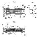
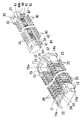
従来より、例えば図7〜図10に示すように、ソケット50とヘッダ70とで構成され、それぞれが実装されたプリント配線板(例えばFPCと硬質基板)の間を電気的に接続するコネクタが提供されている(例えば、特許文献1参照)。
Conventionally, as shown in FIGS. 7 to 10, for example, a connector that includes a
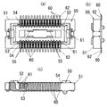
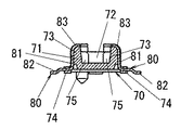
ソケット50は、図7及び図8に示すように、扁平な直方体状に形成された樹脂成型品からなるソケット本体51と、ソケット本体51に配設される複数のソケットコンタクト60とを具備する。ソケット本体51には長手方向に沿って差込溝52が形成され、この差込溝52の底面から細長の直方体状の突台部53が略垂直に突設されている。そして、差込溝52の両側の周壁54,54にはソケット本体11の長手方向に沿って複数のソケットコンタクト60が2列に並設されている。
As shown in FIGS. 7 and 8, the
ソケットコンタクト60は帯状の金属材を曲成することによって形成され、差込溝52内に臨む一端部にはヘッダコンタクト80に接触する接触部61が形成されており、ソケット本体11の樹脂成形時にインサートされている。また、差込溝52の外側に位置するソケットコンタクト60の一端側は、ソケット本体51の背面側(プリント配線板側)から外側に曲げられて周壁54と略垂直な方向に突出し、プリント配線板の導電パターンに半田固定される端子部62を先端部に形成してある。
The
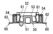
一方、ヘッダ70は、図9及び図10に示すように、扁平な直方体状に形成された樹脂成型品からなるヘッダ本体71と、ヘッダ本体71に配設されて複数のソケットコンタクト60にそれぞれ接触導通する複数のヘッダコンタクト80とを具備する。ヘッダ本体71には、ソケット本体51の突台部53と対向する部位に、この突台部53と嵌合する嵌合溝72がヘッダ本体71の長手方向に沿って形成されている。そして、ヘッダ本体71の嵌合溝72の両側の周壁73,73には、ヘッダ本体71の背面側(プリント配線板側)の縁に、周壁73から略垂直に突出する鍔部74が形成されている。また嵌合溝72の溝内には、嵌合時に加わる衝撃を分散させるために突台部53に設けたキー溝55に嵌合する嵌合突起75が4箇所に突設されている。
On the other hand, as shown in FIGS. 9 and 10, the
ヘッダコンタクト80は、帯状の金属材を曲成することによって形成され、周壁73の外表面に沿った部位の鍔部74側にはソケットコンタクト60の接触部61に接触する接触部81が形成され、鍔部74から突出する一端部にはプリント配線板の導電パターンに半田固定される端子部82が形成されており、インサート成形によりヘッダ本体71に同時成形されている。
The
このソケット50とヘッダ70とは、それぞれプリント配線板の導電パターンに、各ソケットコンタクト60の端子部62、各ヘッダコンタクト80の端子部82を半田固定することで実装される。そして、ヘッダ70をソケット50の差込溝52に挿入すると、ヘッダ70の嵌合溝72にソケット50の突台部53が嵌合するとともに、ソケットコンタクト60の接触部61がヘッダコンタクト80の接触部81に弾接して、ソケット50が実装されたプリント配線板とヘッダ70が実装されたプリント配線板の間が電気的に接続されるのである。
上記構成のコネクタでは、ソケット本体51にヘッダ本体71を接続するための差込溝52が形成されているので、ソケット本体51の機械的強度が弱く、変形しやすいという問題があり、ソケット本体51の機械的強度を高めるために、差込溝52内に突台部53を設け、この突台部53が嵌る嵌合溝72をヘッダ本体71に設けていた。そのため、突台部53の寸法だけソケット本体51およびヘッダ本体71の短手方向の寸法が大きくなるという問題があった。
In the connector having the above configuration, since the insertion groove 52 for connecting the
ところで、このコネクタはコンタクトのピッチが例えば0.4mm程度の狭ピッチのもので、携帯端末などの小型の電子機器に用いられるものであるが、電子機器のさらなる小型化のために、より小型のコネクタが要求されている。コネクタの長手方向(コンタクトの配列方向)の寸法はコンタクトのピッチや本数によって決まり、コンタクトのピッチは絶縁距離を確保するためにある程度の距離が必要であるから、コネクタを小型化するためには短手方向の寸法を小さくする必要がある。 By the way, this connector has a narrow contact pitch of about 0.4 mm, for example, and is used for small electronic devices such as portable terminals. A connector is requested. The length of the connector in the longitudinal direction (contact arrangement direction) is determined by the contact pitch and the number of contacts, and the contact pitch requires a certain distance to secure the insulation distance. It is necessary to reduce the dimensions in the hand direction.
そこで、ソケット本体51およびヘッダ本体71にそれぞれ補強金具を圧入により固定することで成型品の強度を高め、突台部53を無くして短手方向の寸法を短くすることが考えられるが、ソケットコンタクト60およびヘッダコンタクト80をインサート成形可能な寸法範囲でソケット本体51およびヘッダ本体71の短手方向寸法を最小にすると、ヘッダコンタクト80の先端部の角に設けた曲面部83の曲率半径が小さくなり、コネクタの嵌合時にソケットコンタクト60の先端(すなわち接触部61の先端)がヘッダコンタクト80の曲面部83に引っ掛かって、曲面部83上を摺接しながら所定の接触位置まで移動することができず、ソケットコンタクト60の接触部61が座屈してしまう虞があった。
Therefore, it is conceivable to increase the strength of the molded product by fixing the reinforcing metal fittings to the socket
またヘッダコンタクト80の接触部81は、ヘッダ本体71の周壁73に沿って配置されており、接触部81の先端部(すなわち曲面部83の端部)がヘッダ本体71に係止する構造になっていないため、ヘッダ70を斜めに抜き差しすると、ヘッダ本体71が変形して、接触部81の先端側が周壁73から浮き上がって剥がれてしまうという問題もあった。
The
本発明は上記問題点に鑑みて為されたものであり、その目的とするところは、コネクタ嵌合時のソケットコンタクトの座屈を防止するとともに、ヘッダコンタクトの剥がれを防止した小型のコネクタを提供することにある。 The present invention has been made in view of the above problems, and an object of the present invention is to provide a small connector that prevents buckling of the socket contact and prevents peeling of the header contact when the connector is fitted. There is to do.
上記目的を達成するために、本発明は、絶縁部材からなるヘッダ本体を具備したヘッダと、絶縁部材からなりヘッダが挿抜される差込溝が設けられたソケット本体を具備したソケットとを含み、ヘッダ本体の挿抜方向に沿う外表面に1乃至複数のヘッダコンタクトを保持させるとともに、差込溝にヘッダが挿入された際に差込溝の内側においてヘッダコンタクトに接触導通するように1乃至複数のソケットコンタクトをソケット本体に保持させたコネクタにおいて、ヘッダ本体におけるソケット本体との対向面に取付溝を形成するとともに、ヘッダコンタクトに、外表面に配置されてソケットコンタクトに接触する接触部と、該接触部の先端側からU字状に延出し、ヘッダ本体における取付溝の端面と外表面との間の部位を挟むようにしてヘッダ本体に取り付けられる取付部とを設け、取付部においてソケットコンタクトが接触する曲面部分の曲率半径を、少なくともソケットコンタクトが曲面部分に引っ掛かって座屈しないような最小の曲率半径としたことを特徴とする。 To achieve the above object, the present invention includes a header having a header body made of an insulating member, and a socket having a socket body made of an insulating member and provided with an insertion groove into which the header is inserted and removed. One or more header contacts are held on the outer surface along the insertion / removal direction of the header body, and when the header is inserted into the insertion groove, the one or more header contacts are electrically connected to the header contact inside the insertion groove. In the connector in which the socket contact is held on the socket body, a mounting groove is formed on the surface of the header body facing the socket body, the header contact is disposed on the outer surface, and the contact portion is in contact with the socket contact; It extends in a U shape from the front end side of the section, and sandwiches the portion between the end surface of the mounting groove in the header body and the outer surface. And the curvature radius of the curved surface portion where the socket contact comes into contact with the mounting portion is set to the minimum curvature radius so that the socket contact is not caught and buckled by the curved surface portion. To do.
本発明によれば、ヘッダコンタクトに設けたU字状の取付部が、ヘッダ本体における取付溝の端面と外表面との間の部位を挟むようにしてヘッダ本体に取り付けられているので、ヘッダの挿抜時にヘッダ本体が変形したとしても取付部の先端が取付溝の端面に係止しているから、ヘッダコンタクトがヘッダ本体から剥がれるのを防止できるという効果がある。そのうえ、取付部におけるソケットコンタクトと接触する曲面部分の曲率半径が、少なくともソケットコンタクトが曲面部分に引っ掛かって座屈しないような最小の曲率半径に形成されているので、ソケットコンタクトの座屈を防止しつつ、短手方向の寸法を小さくして、小型のコネクタを実現できるという効果もある。 According to the present invention, the U-shaped mounting portion provided in the header contact is mounted on the header body so as to sandwich the portion between the end surface of the mounting groove and the outer surface of the header body. Even if the header body is deformed, the tip of the mounting portion is locked to the end surface of the mounting groove, so that it is possible to prevent the header contact from being peeled off from the header body. In addition, the curvature radius of the curved surface part that contacts the socket contact in the mounting portion is formed at least so that the socket contact does not buckle due to being caught by the curved surface part, so that the socket contact is prevented from buckling. However, there is also an effect that a small connector can be realized by reducing the dimension in the short direction.
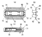
以下に本発明の実施の形態を図1〜図6に基づいて説明する。本実施形態のコネクタは、例えばフレキシブルプリント配線板と硬質基板であるプリント配線板との間を接続する基板対基板のコネクタであり、図6に示すように複数のソケットコンタクト20および各ソケットコンタクト20が並べて配設されたソケット本体11を具備したソケット10と、各ソケットコンタクト20に接触導通する複数のヘッダコンタクト40および各ヘッダコンタクト40が並べて配設されるヘッダ本体31を具備したヘッダ30とで構成される。
Embodiments of the present invention will be described below with reference to FIGS. The connector of the present embodiment is a board-to-board connector that connects, for example, a flexible printed wiring board and a printed wiring board that is a rigid board, and includes a plurality of
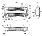
ソケット10のソケット本体11は、図4及び図5に示すように、扁平な略直方体状に形成された樹脂成型品からなり、ソケット本体11の長手方向に沿って矩形状に凹没した差込溝12が形成されている。ソケット本体11の樹脂成形時には複数のソケットコンタクト20がインサートされており、複数のソケットコンタクト20はソケット本体11の長手方向に沿って差込溝12の両側の周壁13,13に2列に並設されている。また、ソケット本体11におけるヘッダ30との対向面には、差込溝12の長手方向両端部の周縁から、ヘッダ30側に向かってコ字状のガイド壁15が突設されており、このガイド壁15には差込溝12から外側に行くほど突出量が大きくなるような傾斜面15aが形成されている。
As shown in FIGS. 4 and 5, the
各ソケットコンタクト20は帯状の金属材からなり、U字状に曲成されてソケット本体11の差込溝12周辺の長手方向に沿う周壁13の縁部を挟む形でソケット本体11に保持された保持部21と、保持部21における差込溝12の内側に位置する一端から保持部21とともにS字状を形成する形で延設され保持部21との間の距離を変化させる方向(すなわち、差込溝12へのヘッダ30の挿抜方向と交差する方向)に撓み可能な撓み部22と、保持部21における差込溝12の外側に位置する一端から外側に曲げられて周壁13と略垂直な方向に突出し、例えばプリント配線板の導電パターンに半田固定される帯状の端子部23とが連続一体に設けられている。また撓み部22には、保持部21から離れる方向に突出した接触凸部24(接触部)が曲げにより形成されており、この接触凸部24は上記挿抜方向と交差する方向に弾性的に突出している(図5参照)。
Each
また、ソケット本体11の長手方向の両端部には端子補強金具14がインサート成形により同時成形されている。端子補強金具14はソケット本体11の長手方向の両端部の底部から側方に突出する固定片14aと、長手方向の両端部にある一対の固定片14aの間を連結し、ソケット本体11内に埋設固定されるU字形の連結片14bとを備え、固定片14aは端子部23と略同一高さに配置されている。而してソケット10の端子部23をプリント配線板の導電パターンに半田固定する際に、固定片14aをプリント配線板のランドに半田固定することで、ソケット本体11の基板への固定強度を補強することができ、コネクタ嵌合時にソケットコンタクト20に加わるストレスを低減できる。
Moreover, the terminal
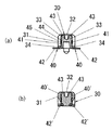
一方、ヘッダ30のヘッダ本体31は、図2及び図3に示すように、細長の略直方体状に形成された樹脂成型品からなり、ソケット本体11との対向面における短幅方向の中央部には、ヘッダコンタクト40が配設される部位に取付溝32が長手方向に沿って形成され、取付溝32の両側にある周壁33,33の背面側(ソケット10と反対側)の縁には周壁33から略垂直に突出する鍔部34が形成されている。そして、ヘッダ本体31の周壁33,33の外側面には、ヘッダ本体31の長手方向に沿って複数のヘッダコンタクト40が2列に並設されている。また取付溝32の溝内には、取付溝32の底部から開口部にかけて取付溝32を挟んで対向する周壁33,33の間を連結する複数の隔壁35がヘッダ本体31と一体に形成されており、各々の隔壁35はヘッダ本体31の長手方向において隣接するヘッダコンタクト40の間に配置されている。
On the other hand, as shown in FIGS. 2 and 3, the
各ヘッダコンタクト40は帯状の金属材を曲成することによって形成され、インサート成形によりヘッダ本体31に同時成形されており、ヘッダ本体31の背面側(基板側)の一端側が、鍔部34から周壁33と略垂直な方向に突出している。そして、各ヘッダコンタクト40には、周壁33の挿抜方向(図1の上下方向)に沿う外表面の鍔部34側に配置されて、ソケットコンタクト20の接触凸部24に接触する接触部41が形成されており、この接触部41の背面側から側方に延出し鍔部34から突出する一端部に、プリント配線板の導電パターンに半田固定される帯状の端子部42が形成されている。また、各ヘッダコンタクト40には、接触部41の先端側(ソケット10側)からU字状に延出し、取付溝32の端面と上記外表面との間の部位(すなわち周壁33)を挟むようにしてヘッダ本体31に取り付けられる取付部43が設けられており、ソケットコンタクト20の撓み部22に接触する取付部43の曲面部分(外表面側の曲がり部)の曲率半径を、撓み部22がこの曲面部分に引っ掛かって座屈しないような最小の曲率半径に設定してある。
Each
またヘッダ本体31の長手方向の両端部には、ヘッダコンタクト40のインサート成形時にロスピンとなるヘッダコンタクト40’をインサート成形により同時成形してあり、このヘッダコンタクト40’の端子部42’の先端位置がヘッダ本体31の短手方向の両側面と略同じになるように、他の信号接続用の端子部42に比べて端子部42’を短めに切断してある。そして、ヘッダコンタクト40の端子部42をプリント配線板の導電パターンに半田固定する際に、端子部42’をプリント配線板のランド49に半田固定することで、ヘッダ本体31の基板への固定強度を補強することができ、コネクタ嵌合時にヘッダコンタクト40に加わるストレスを低減できる。すなわちロスピンとなるヘッダコンタクト40’の端子部42’が端子補強金具として機能する。
In addition,
本実施形態のコネクタは上記のような構成を有し、ソケットコンタクト20の端子部23およびヘッダコンタクト40の端子部42を、それぞれプリント配線板のような別々の基板(図示せず)に半田固定し、ソケット本体11の差込溝12にヘッダ30を差し込んで複数のソケットコンタクト20とヘッダコンタクト40とを各別に接触させることによって、プリント配線板の間を電気的に接続するのである。
The connector according to the present embodiment has the above-described configuration, and the
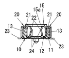
ここで、ソケット嵌合時にはソケットコンタクト20の接触凸部24が、ヘッダコンタクト40の先端部に設けたU字状の取付部43の外表面側の曲面部分に当接するのであるが、この曲面部分の曲率半径は、少なくともソケットコンタクト20がこの曲面部分に引っ掛かって座屈しないような最小の曲率半径に形成されているので、ソケットコンタクト20の座屈を防止しつつ、ヘッダ本体31の短手方向の寸法を小さくでき、コネクタの小型化を図ることができる。また、U字状の取付部43は、取付溝32の両側にある周壁33を挟むようにしてヘッダ本体31に取り付けられており、取付部43の一端が取付溝32の端面に係止しているので、コネクタ嵌合時にヘッダ本体31が変形したとしても、ヘッダコンタクト40がヘッダ本体31の表面から浮き上がって、剥がれることはない。
Here, when the socket is fitted, the contact
また、ソケット本体11の差込溝12にヘッダ30を差し込む際には、差込溝12の周縁部に設けたガイド壁15の傾斜面15aにヘッダ30がガイドされて、差込溝12に挿入されるため、ソケット本体11とヘッダ本体31との相対位置が多少ずれたとしても、ヘッダ30を差込溝12に容易に差し込めるようになっている。
When inserting the
またヘッダコンタクト40の接触部41において、ソケットコンタクト20の接触凸部24と接触する部位には突起44と凹部45が設けられており、図1に示すように、ヘッダ30がソケット10の差込溝12の奥まで挿入された状態において、接触凸部24は凹部45の両側部に接触しており、突起44は接触凸部24よりも差込溝12の底面側に位置している。突起44は、接触部41の端子部42が突出する側の面において長さ方向の中間よりも端子部42から離れた位置に突設されており、この突起44には、突出寸法を端子部42に近い位置ほど大きくする傾斜面44aが設けられている。また、凹部45は、図2(c)に示すように、接触凸部24の摺動方向に沿って延びた溝状であって、凹部45の内側にはそれぞれ接触凸部24の摺動方向に交差する方向(図中の左右方向)の端に近づくほど凹部45の深さ寸法を小さくする2つの平面である傾斜面が形成されており、凹部45の左右方向の断面形状をV字状に形成してある。
Further, in the
ここで、接触凸部24の摺動方向に交差する方向における凹部45の幅寸法は、接触凸部24の幅寸法よりも小さく形成され、凹部45は接触部41において接触凸部24の摺動範囲内に設けられており、ヘッダ30をソケット10の差込溝12に挿入する過程においては、接触部41における凹部45の両側部に接触凸部24が弾接する。また、接触凸部24において、突起44に接触する範囲と凹部45の両側部に接触する範囲とが重ならないように、ヘッダコンタクト40の幅方向における突起44の幅寸法は、凹部45の幅寸法よりもさらに小さく設定されている。
Here, the width dimension of the
この構成によれば、ソケット10とヘッダ30とが結合される前にソケットコンタクト20の接触凸部24やヘッダコンタクト40の接触部41に異物が付着していても、接触凸部24が接触部41の表面上を摺動する過程において異物を凹部45内に落としこめるから、凹部45が設けられていない場合に比べて接触凸部24と接触部41との間に異物が挟まる可能性が低くなる。つまり、異物による接触不良が防止され、且つ接触凸部24が凹部45の両側の2点で接触するから、接触信頼性を向上することができる。また、接触部41において接触凸部24の摺動範囲内に凹部45が設けられているので、接触凸部24の摺動範囲から外れた位置に凹部45を設ける場合に比べ、接触凸部24に付着した異物をより凹部45に落としこみやすい。
According to this configuration, even if foreign matter adheres to the contact
また、ヘッダ30を差込溝12から抜く力が加わると、ソケットコンタクト20の接触凸部24がヘッダコンタクト40の突起44に当接して抵抗力が付与されるから、コネクタが振動などを受けてもヘッダ30が差込溝12から抜けにくいという利点がある。なお、ヘッダ30を差込溝12に挿入する際にもソケットコンタクト20の接触凸部24はヘッダコンタクト40の突起44に当接するが、突起44の突出寸法を端子部42から離れた位置ほど小さくする傾斜面44aが突起44に設けられているので、ヘッダ30を差込溝12に挿入する際の抵抗はヘッダ30を差込溝12から抜く際の抵抗よりも小さくなる。また、接触凸部24において、突起44に接触する範囲と凹部45の両側部に接触する範囲とが重ならないように凹部45の位置と形状とを設定してあるから、接触凸部24が突起44の表面を摺動する際に接触凸部24に押された異物は凹部45に落としこめられ、接触凸部24と接触部41との間に挟まることがない。
Further, when a force for pulling out the
なお、本実施形態では接触凸部24が接触部41における凹部45の両側部に弾接しており、接触凸部24が接触部41の表面上を摺動する過程で異物を凹部45内に落とし込むことで接触凸部24と接触部41との間に異物が挟まる可能性を低減して、接触信頼性を向上させているが、接触凸部24と接触部41の形状およびその接触状態を上記の形態に限定する趣旨のものではなく、接触凸部24の接触部41に接触する面を、幅方向の中間部が両端部よりも接触部41側に突出するような形状(例えば曲面形状)に形成することで、幅方向の中間部が接触部41に設けた凹部45内に進入して、凹部45内の2つの傾斜面、又は、凹部45の開口縁に2点で接触するようにしても良く、接触凸部24と接触部41とが互いに平面で接触する場合に比べて接触凸部24と接触部41との接触面積が小さくなって、接触圧が増大するから、接触凸部24と接触部41との間から異物が排出されやすくなって、接触信頼性が向上する。
In this embodiment, the contact
10 ソケット
20 ソケットコンタクト
30 ヘッダ
31 ヘッダ本体
32 取付溝
33 周壁
40 ヘッダコンタクト
41 接触部
43 取付部
DESCRIPTION OF
Claims (1)
Including a header having a header body made of an insulating member, and a socket having a socket body made of an insulating member and provided with an insertion groove into which the header is inserted and removed, and on an outer surface along the insertion / extraction direction of the header body One or more socket contacts are held in the socket body so that the header contacts are held in contact with the header contact inside the insertion groove when the header is inserted into the insertion groove. In the connector held by the connector, a mounting groove is formed on a surface of the header main body facing the socket main body, and the header contact is disposed on the outer surface and contacts with the socket contact, the contact Between the end surface of the mounting groove in the header body and the outer surface. A mounting portion that is attached to the header body so as to sandwich the part, and the curvature radius of the curved surface portion that contacts the socket contact in the mounting portion is at least the minimum that the socket contact is caught by the curved surface portion and does not buckle A connector characterized by a curvature radius of.
Priority Applications (8)
| Application Number | Priority Date | Filing Date | Title |
|---|---|---|---|
| JP2004107303A JP2005294034A (en) | 2004-03-31 | 2004-03-31 | Connector |
| US10/558,486 US7195494B2 (en) | 2004-03-31 | 2005-03-28 | Connector for electrically connecting electronic components |
| KR1020057020390A KR100753922B1 (en) | 2004-03-31 | 2005-03-28 | Connector |
| EP05727403.7A EP1732170B1 (en) | 2004-03-31 | 2005-03-28 | Connector |
| CNB2005800002097A CN100442603C (en) | 2004-03-31 | 2005-03-28 | Connector |
| PCT/JP2005/005750 WO2005096445A1 (en) | 2004-03-31 | 2005-03-28 | Connector |
| TW094110024A TWI251375B (en) | 2004-03-31 | 2005-03-30 | Connector |
| CNU2005200045687U CN2789959Y (en) | 2004-03-31 | 2005-03-31 | Connector |
Applications Claiming Priority (1)
| Application Number | Priority Date | Filing Date | Title |
|---|---|---|---|
| JP2004107303A JP2005294034A (en) | 2004-03-31 | 2004-03-31 | Connector |
Publications (1)
| Publication Number | Publication Date |
|---|---|
| JP2005294034A true JP2005294034A (en) | 2005-10-20 |
Family
ID=35064101
Family Applications (1)
| Application Number | Title | Priority Date | Filing Date |
|---|---|---|---|
| JP2004107303A Pending JP2005294034A (en) | 2004-03-31 | 2004-03-31 | Connector |
Country Status (7)
| Country | Link |
|---|---|
| US (1) | US7195494B2 (en) |
| EP (1) | EP1732170B1 (en) |
| JP (1) | JP2005294034A (en) |
| KR (1) | KR100753922B1 (en) |
| CN (2) | CN100442603C (en) |
| TW (1) | TWI251375B (en) |
| WO (1) | WO2005096445A1 (en) |
Cited By (3)
| Publication number | Priority date | Publication date | Assignee | Title |
|---|---|---|---|---|
| JP2008084795A (en) * | 2006-09-29 | 2008-04-10 | Omron Corp | connector |
| KR100862020B1 (en) | 2005-12-15 | 2008-10-07 | 마츠시다 덴코 가부시키가이샤 | Connector |
| JP2013134968A (en) * | 2011-12-27 | 2013-07-08 | Toshiba Corp | Electronic apparatus |
Families Citing this family (22)
| Publication number | Priority date | Publication date | Assignee | Title |
|---|---|---|---|---|
| JP2005294034A (en) * | 2004-03-31 | 2005-10-20 | Matsushita Electric Works Ltd | Connector |
| JP4563915B2 (en) * | 2005-10-21 | 2010-10-20 | ヒロセ電機株式会社 | Circuit board electrical connector |
| KR100968327B1 (en) * | 2007-03-14 | 2010-07-08 | 파나소닉 전공 주식회사 | Multipole Coaxial Connector |
| JP4386089B2 (en) * | 2007-03-27 | 2009-12-16 | パナソニック電工株式会社 | Mounting structure of connector receptacle on wiring board |
| JP2008270085A (en) * | 2007-04-24 | 2008-11-06 | Matsushita Electric Works Ltd | Connector |
| JP4412347B2 (en) * | 2007-04-24 | 2010-02-10 | パナソニック電工株式会社 | Connector and connector connector |
| CN201060970Y (en) * | 2007-06-11 | 2008-05-14 | 江苏华富电子有限公司 | Electrical connector |
| JP2009120150A (en) * | 2007-11-19 | 2009-06-04 | Aisin Seiki Co Ltd | Electrical contact mechanism |
| CN201160164Y (en) * | 2008-01-05 | 2008-12-03 | 富士康(昆山)电脑接插件有限公司 | electrical connector |
| JP5253129B2 (en) * | 2008-12-19 | 2013-07-31 | モレックス インコーポレイテド | Board to board connector |
| JP4374074B1 (en) * | 2009-06-10 | 2009-12-02 | イリソ電子工業株式会社 | Electrical connection terminal and connector using the same |
| WO2011002186A2 (en) * | 2009-06-29 | 2011-01-06 | 휴먼전자 주식회사 | Board-to-board-type connector |
| JP2012099276A (en) * | 2010-10-29 | 2012-05-24 | Jst Mfg Co Ltd | Contact and connector |
| US8888506B2 (en) * | 2013-01-29 | 2014-11-18 | Japan Aviation Electronics Industry, Limited | Connector |
| US9124011B2 (en) * | 2013-02-27 | 2015-09-01 | Panasonic Intellectual Property Management Co., Ltd. | Connector, and header and socket to be used in the same |
| JP5751434B2 (en) * | 2013-04-19 | 2015-07-22 | Smk株式会社 | Board connection structure using board connector |
| JP6712794B2 (en) * | 2014-08-07 | 2020-06-24 | パナソニックIpマネジメント株式会社 | Connector and header and socket used for the connector |
| JP6473990B2 (en) * | 2014-08-07 | 2019-02-27 | パナソニックIpマネジメント株式会社 | Connector and socket used for the connector |
| JP6537890B2 (en) * | 2014-09-26 | 2019-07-03 | 日本航空電子工業株式会社 | connector |
| JP6287977B2 (en) * | 2015-06-30 | 2018-03-07 | Smk株式会社 | connector |
| JP7364363B2 (en) * | 2019-04-25 | 2023-10-18 | モレックス エルエルシー | connector |
| JP7366653B2 (en) * | 2019-09-06 | 2023-10-23 | 日本航空電子工業株式会社 | Connectors and connector manufacturing methods |
Citations (8)
| Publication number | Priority date | Publication date | Assignee | Title |
|---|---|---|---|---|
| JPH0611268U (en) * | 1992-07-14 | 1994-02-10 | ホシデン株式会社 | Detachable connector |
| JPH06111873A (en) * | 1992-09-25 | 1994-04-22 | Matsushita Electric Works Ltd | Connector |
| JPH11260505A (en) * | 1998-03-13 | 1999-09-24 | Matsushita Electric Works Ltd | Connector |
| JPH11329622A (en) * | 1998-05-20 | 1999-11-30 | Omron Corp | Connector structure |
| JP2002008753A (en) * | 2000-06-16 | 2002-01-11 | Matsushita Electric Works Ltd | Connector |
| JP2003017162A (en) * | 2001-06-26 | 2003-01-17 | Japan Aviation Electronics Industry Ltd | connector |
| JP2004055464A (en) * | 2002-07-23 | 2004-02-19 | Matsushita Electric Works Ltd | Low stature type connector |
| JP2004111081A (en) * | 2002-09-13 | 2004-04-08 | Matsushita Electric Works Ltd | connector |
Family Cites Families (8)
| Publication number | Priority date | Publication date | Assignee | Title |
|---|---|---|---|---|
| JP2561407B2 (en) | 1992-06-25 | 1996-12-11 | 株式会社神戸製鋼所 | Cooling device for high temperature and high pressure vessels |
| JP3617220B2 (en) * | 1996-11-26 | 2005-02-02 | 松下電工株式会社 | connector |
| JP3321553B2 (en) | 1997-10-08 | 2002-09-03 | 松下電器産業株式会社 | Method for manufacturing Bi-CMOS integrated circuit device |
| KR100511180B1 (en) | 2003-02-19 | 2005-08-30 | 재영솔루텍 주식회사 | Production method of electric-connector |
| US6827588B1 (en) * | 2003-06-12 | 2004-12-07 | Cheng Uei Precision Industry Co., Ltd. | Low profile board-to-board connector assembly |
| US6793506B1 (en) * | 2003-08-27 | 2004-09-21 | Molex Incorporated | Board-to-board electrical connector assembly |
| US6811411B1 (en) * | 2003-09-12 | 2004-11-02 | Molex Incorporated | Board-to-board electrical connector assembly |
| JP2005294034A (en) * | 2004-03-31 | 2005-10-20 | Matsushita Electric Works Ltd | Connector |
-
2004
- 2004-03-31 JP JP2004107303A patent/JP2005294034A/en active Pending
-
2005
- 2005-03-28 CN CNB2005800002097A patent/CN100442603C/en not_active Expired - Lifetime
- 2005-03-28 WO PCT/JP2005/005750 patent/WO2005096445A1/en not_active Ceased
- 2005-03-28 EP EP05727403.7A patent/EP1732170B1/en not_active Expired - Lifetime
- 2005-03-28 US US10/558,486 patent/US7195494B2/en not_active Expired - Lifetime
- 2005-03-28 KR KR1020057020390A patent/KR100753922B1/en not_active Expired - Fee Related
- 2005-03-30 TW TW094110024A patent/TWI251375B/en not_active IP Right Cessation
- 2005-03-31 CN CNU2005200045687U patent/CN2789959Y/en not_active Expired - Lifetime
Patent Citations (8)
| Publication number | Priority date | Publication date | Assignee | Title |
|---|---|---|---|---|
| JPH0611268U (en) * | 1992-07-14 | 1994-02-10 | ホシデン株式会社 | Detachable connector |
| JPH06111873A (en) * | 1992-09-25 | 1994-04-22 | Matsushita Electric Works Ltd | Connector |
| JPH11260505A (en) * | 1998-03-13 | 1999-09-24 | Matsushita Electric Works Ltd | Connector |
| JPH11329622A (en) * | 1998-05-20 | 1999-11-30 | Omron Corp | Connector structure |
| JP2002008753A (en) * | 2000-06-16 | 2002-01-11 | Matsushita Electric Works Ltd | Connector |
| JP2003017162A (en) * | 2001-06-26 | 2003-01-17 | Japan Aviation Electronics Industry Ltd | connector |
| JP2004055464A (en) * | 2002-07-23 | 2004-02-19 | Matsushita Electric Works Ltd | Low stature type connector |
| JP2004111081A (en) * | 2002-09-13 | 2004-04-08 | Matsushita Electric Works Ltd | connector |
Cited By (4)
| Publication number | Priority date | Publication date | Assignee | Title |
|---|---|---|---|---|
| KR100862020B1 (en) | 2005-12-15 | 2008-10-07 | 마츠시다 덴코 가부시키가이샤 | Connector |
| JP2008084795A (en) * | 2006-09-29 | 2008-04-10 | Omron Corp | connector |
| US7497697B2 (en) | 2006-09-29 | 2009-03-03 | Omron Corporation | PCB connector including plug and socket contacts for easy positioning |
| JP2013134968A (en) * | 2011-12-27 | 2013-07-08 | Toshiba Corp | Electronic apparatus |
Also Published As
| Publication number | Publication date |
|---|---|
| CN1771630A (en) | 2006-05-10 |
| US20060234525A1 (en) | 2006-10-19 |
| WO2005096445A1 (en) | 2005-10-13 |
| CN100442603C (en) | 2008-12-10 |
| EP1732170A4 (en) | 2008-03-26 |
| KR20060005401A (en) | 2006-01-17 |
| CN2789959Y (en) | 2006-06-21 |
| EP1732170B1 (en) | 2013-06-26 |
| TW200534540A (en) | 2005-10-16 |
| EP1732170A1 (en) | 2006-12-13 |
| US7195494B2 (en) | 2007-03-27 |
| KR100753922B1 (en) | 2007-08-31 |
| TWI251375B (en) | 2006-03-11 |
Similar Documents
| Publication | Publication Date | Title |
|---|---|---|
| JP2005294034A (en) | Connector | |
| JP2005294035A (en) | Connector | |
| JP2005294036A (en) | Connector and its manufacturing method | |
| EP1096609B1 (en) | Locking mechanism for securely preventing disconnection between a plug and a receptacle | |
| CN103098307B (en) | Board-to-Board Connector | |
| CN202633548U (en) | Board-to-Board Connector | |
| US7172434B2 (en) | Electrical connection apparatus capable of resisting repetition of connection and disconnection | |
| US9065228B2 (en) | Connector | |
| CN102292874B (en) | Board-to-board connector | |
| CN103155292B (en) | Board to board connector | |
| CN102227851B (en) | Board-to-Board Connector | |
| KR20200008840A (en) | receptacle connector | |
| CN102124607B (en) | Board connector | |
| US8277228B2 (en) | Connector set and jointer for use therein | |
| JP6712799B2 (en) | Connector and header and socket used for the connector | |
| CN103168395A (en) | Circuit board-circuit board connector | |
| JP4851510B2 (en) | Electrical connector | |
| JP2023001183A (en) | Metal fitting, connector with metal fitting, and connector assembly | |
| JP2004527069A (en) | Small board-to-board connector | |
| WO2004049520A1 (en) | Electrical connector for board, method of molding electrical connector housing for board, and metal mold for injection molding of electrical connector housing | |
| JP2009289627A (en) | Connector | |
| US9093799B2 (en) | Connector apparatus | |
| JP2007149708A (en) | Manufacturing method of connector | |
| JP2007287589A (en) | Electrical connector | |
| CN110838628B (en) | Disposable anti-theft connector |
Legal Events
| Date | Code | Title | Description |
|---|---|---|---|
| A621 | Written request for application examination |
Free format text: JAPANESE INTERMEDIATE CODE: A621 Effective date: 20060403 |
|
| A131 | Notification of reasons for refusal |
Free format text: JAPANESE INTERMEDIATE CODE: A131 Effective date: 20070116 |
|
| A02 | Decision of refusal |
Free format text: JAPANESE INTERMEDIATE CODE: A02 Effective date: 20070522 |