JP4563915B2 - Circuit board electrical connector - Google Patents
Circuit board electrical connector Download PDFInfo
- Publication number
- JP4563915B2 JP4563915B2 JP2005307101A JP2005307101A JP4563915B2 JP 4563915 B2 JP4563915 B2 JP 4563915B2 JP 2005307101 A JP2005307101 A JP 2005307101A JP 2005307101 A JP2005307101 A JP 2005307101A JP 4563915 B2 JP4563915 B2 JP 4563915B2
- Authority
- JP
- Japan
- Prior art keywords
- connector
- fitting
- housing
- mating
- terminal
- Prior art date
- Legal status (The legal status is an assumption and is not a legal conclusion. Google has not performed a legal analysis and makes no representation as to the accuracy of the status listed.)
- Active
Links
- 230000013011 mating Effects 0.000 claims description 63
- 238000005452 bending Methods 0.000 claims description 7
- 239000002184 metal Substances 0.000 claims description 4
- 239000000758 substrate Substances 0.000 description 4
- 230000004308 accommodation Effects 0.000 description 3
- 238000005476 soldering Methods 0.000 description 2
- 239000004020 conductor Substances 0.000 description 1
- 230000000694 effects Effects 0.000 description 1
- 239000012777 electrically insulating material Substances 0.000 description 1
- 238000007654 immersion Methods 0.000 description 1
- 239000012212 insulator Substances 0.000 description 1
- 230000002452 interceptive effect Effects 0.000 description 1
- 238000000034 method Methods 0.000 description 1
- 230000000149 penetrating effect Effects 0.000 description 1
- 230000002093 peripheral effect Effects 0.000 description 1
- 238000003825 pressing Methods 0.000 description 1
- 238000004080 punching Methods 0.000 description 1
Images


Classifications
-
- H—ELECTRICITY
- H01—ELECTRIC ELEMENTS
- H01R—ELECTRICALLY-CONDUCTIVE CONNECTIONS; STRUCTURAL ASSOCIATIONS OF A PLURALITY OF MUTUALLY-INSULATED ELECTRICAL CONNECTING ELEMENTS; COUPLING DEVICES; CURRENT COLLECTORS
- H01R12/00—Structural associations of a plurality of mutually-insulated electrical connecting elements, specially adapted for printed circuits, e.g. printed circuit boards [PCB], flat or ribbon cables, or like generally planar structures, e.g. terminal strips, terminal blocks; Coupling devices specially adapted for printed circuits, flat or ribbon cables, or like generally planar structures; Terminals specially adapted for contact with, or insertion into, printed circuits, flat or ribbon cables, or like generally planar structures
- H01R12/50—Fixed connections
- H01R12/59—Fixed connections for flexible printed circuits, flat or ribbon cables or like structures
- H01R12/594—Fixed connections for flexible printed circuits, flat or ribbon cables or like structures for shielded flat cable
- H01R12/598—Each conductor being individually surrounded by shield, e.g. multiple coaxial cables in flat structure
-
- H—ELECTRICITY
- H01—ELECTRIC ELEMENTS
- H01R—ELECTRICALLY-CONDUCTIVE CONNECTIONS; STRUCTURAL ASSOCIATIONS OF A PLURALITY OF MUTUALLY-INSULATED ELECTRICAL CONNECTING ELEMENTS; COUPLING DEVICES; CURRENT COLLECTORS
- H01R12/00—Structural associations of a plurality of mutually-insulated electrical connecting elements, specially adapted for printed circuits, e.g. printed circuit boards [PCB], flat or ribbon cables, or like generally planar structures, e.g. terminal strips, terminal blocks; Coupling devices specially adapted for printed circuits, flat or ribbon cables, or like generally planar structures; Terminals specially adapted for contact with, or insertion into, printed circuits, flat or ribbon cables, or like generally planar structures
- H01R12/50—Fixed connections
- H01R12/59—Fixed connections for flexible printed circuits, flat or ribbon cables or like structures
- H01R12/62—Fixed connections for flexible printed circuits, flat or ribbon cables or like structures connecting to rigid printed circuits or like structures
-
- H—ELECTRICITY
- H01—ELECTRIC ELEMENTS
- H01R—ELECTRICALLY-CONDUCTIVE CONNECTIONS; STRUCTURAL ASSOCIATIONS OF A PLURALITY OF MUTUALLY-INSULATED ELECTRICAL CONNECTING ELEMENTS; COUPLING DEVICES; CURRENT COLLECTORS
- H01R2103/00—Two poles
Landscapes
- Coupling Device And Connection With Printed Circuit (AREA)
- Details Of Connecting Devices For Male And Female Coupling (AREA)
Description
本発明は、回路基板に取りつけられて使用される回路基板用電気コネクタに関する。 The present invention relates to an electrical connector for a circuit board that is used by being attached to a circuit board.
この種のコネクタとしては、添付図面の図7に開示されているコネクタが知られている。 As this type of connector, a connector disclosed in FIG. 7 of the accompanying drawings is known.
この図7のコネクタ50は、上方に開口し、底壁52Aを有する収容溝52がハウジング51に形成され、ここに端子53の一部が収容されている。収容溝52は上方に開口されていると共に、ハウジング51の側壁部54の上部が切り落されていて、ここでも側方に開口されている。この収容溝52は、屈曲帯状の端子53の幅に相当する寸法で、紙面に直角な方向での幅が定められている。
The
端子53は、帯状体を略S字状に屈曲され、すなわち、U字状部と逆U字状部とを連続して有する形態をなし、U字状部で弾性腕部53Aを、そして逆U字状部で嵌着部53Bを形成している。該嵌着部53Bは上記側壁部54に対して上方から嵌着される。ハウジング外では、この嵌着部53Bにつながって接続部53Cが設けられていて、回路基板に接面するようになっている。又、上記収容溝52内では上記弾性腕部53Aの先端側が局部的に弯曲されていて接触部53A1をなしている。
The
上記弾性腕部53Aは、収容溝52の底壁52Aに近接して沿う下部53A2を有していて、上記収容溝52内に大きくひろがり、そのU字状の内側に相手コネクタの嵌合接触部61を受入れて、該弾性腕部53Aの先端部に弯曲して形成された接触部53A1が上記嵌合接触部61に対して弾圧接触するようになっている。
The
相手コネクタの嵌合接触部61は、上記弾性腕部53Aの下部53Aの直上方位置にまで進入する。
The
さらに、特許文献1では、上述した図7の形態に類似してはいるが、図7で二点鎖線Aで示されているように、収容溝52を下方まで貫通させて底壁52Aを除去して、端子53の位置をさらに下方に位置せしめている。
この種のコネクタは、横方向寸法は然程問題とされないが、縦方向寸法、すなわち回路基板上での高さ寸法を極力小さくすることが求められる。これは、同様な回路基板を複数段重ねて構成される電子機器を小型化するためである。 In this type of connector, the lateral dimension is not so much a problem, but the vertical dimension, that is, the height dimension on the circuit board is required to be as small as possible. This is to reduce the size of an electronic device configured by stacking a plurality of similar circuit boards.
しかしながら、上述した図7のコネクタでは、回路基板上に配されたコネクタの端子のU字状弾性腕部の上方に相手コネクタの嵌合接触部が位置するので、弾性腕部の下部と嵌合接触部の下部とが上下方向で重なるようになってしまい、その分だけ高さ方向に大きなコネクタとなってしまう。 However, in the connector of FIG. 7 described above, since the mating contact portion of the mating connector is located above the U-shaped elastic arm portion of the connector terminal arranged on the circuit board, it is fitted to the lower portion of the elastic arm portion. The lower part of the contact portion overlaps in the vertical direction, and accordingly, the connector becomes large in the height direction.
一方、特許文献1では、収容溝底部をなすハウジング底壁を除去して収容溝を下方に貫通させているので、その分だけ端子を下方に下げられて、コネクタとしては高さ方向寸法を小さくできる。しかしながら、こうすることにより、端子は回路基板の面に直接至近することとなり、回路基板の対応領域に該端子と係りない回路部があるとすれば、何らかの原因でこの回路部とショートする危険がある。したがって、この特許文献1のコネクタは、上記回路基板の対応領域に回路部を設けないようにして用いられる。これは、回路基板の設計に制約を加えるという不都合をもたらす。 On the other hand, in Patent Document 1, since the housing bottom wall forming the bottom of the housing groove is removed and the housing groove is penetrated downward, the terminal can be lowered by that much, and the height dimension of the connector is reduced. it can. However, by doing so, the terminal is directly close to the surface of the circuit board, and if there is a circuit part that is not related to the terminal in the corresponding area of the circuit board, there is a risk of shorting with this circuit part for some reason. is there. Therefore, the connector of Patent Document 1 is used without providing a circuit portion in the corresponding region of the circuit board. This introduces the disadvantage of limiting the circuit board design.
本発明は、このような回路基板へ設けた際の上記の不都合をもたらすことなく、高さ寸法の小さい回路基板用電気コネクタを提供することを目的とする。 An object of the present invention is to provide an electrical connector for a circuit board having a small height without causing the above-described disadvantages when it is provided on such a circuit board.
本発明は、回路基板上に取りつけられる電気コネクタであって、相手コネクタの嵌合受入れのためにハウジングの長手方向に延び上方に開口して該ハウジングに形成された有底の嵌合凹部の上記長手方向に延び対向せる二つの内側面のうちの一方の内側面に、相手端子と接続される端子の接触部が配列されている電気コネクタに関する。 The present invention, circuit an electrical connector mounted on a substrate, the above-mentioned bottomed fitting recess formed in said housing open upwardly extending longitudinally of the housing for mating acceptance of the mating connector The present invention relates to an electrical connector in which a contact portion of a terminal connected to a mating terminal is arranged on one inner surface of two inner surfaces facing and extending in the longitudinal direction.
かかる電気コネクタにおいて、本発明では、ハウジングは上記一方の内側面を形成する一方のハウジング側壁部に該内側面から没入して端子の弾性腕部を収容する収容溝が嵌合凹部の開口位置から底部位置まで及んで形成され、他方の内側面を形成する他方のハウジング側壁部の側では、該他方の側壁部を越えて相手コネクタのケーブルが延出可能となっており、端子は、板状金属部材をその板厚方向に屈曲して作られており、上記一方のハウジング側壁部に対して上方から嵌着される嵌着部と、該嵌着部につながり上記一方のハウジング側壁部の外面位置から回路基板に接面する位置まで延出する接続部と、上記嵌着部から嵌合凹部内方へ向け延びる上記弾性腕部とを有し、上記嵌着部は上記一方のハウジング側壁部の外面、上面そして上記収容溝の奥部にそれぞれ沿って逆U字状をなし、上記弾性腕部は上記嵌着部から屈曲して延びてU字状をなし、その屈曲部がコネクタ嵌合方向で収容溝の底部にまで達し、該弾性腕部は上記屈曲部から収容溝内で上方に延びて自由端までの間で可撓で弾性を有していて嵌合凹部の上記一方の内側面から若干突出している接触部を有し、上記嵌合凹部は、上記一方の内側面とこれに対向する他方の内側面との間に、相手コネクタの嵌合接触部の進入する空間を形成し、コネクタ嵌合時に、この相手コネクタの嵌合接触部が上記端子の接触部を収容溝内方へ圧しかつコネクタ嵌合方向における該嵌合接触部の先端部が上記端子の屈曲部とほぼ同じ位置まで嵌合凹部の底部へ向け進入するようになっており、さらに、端子は嵌着部が一方のハウジング側壁部の外面に沿って延びる範囲の少なくとも一部で副接触部を形成し、コネクタ嵌合時に、相手コネクタのハウジングに固定された相手端子の逆U字状部分が上記接触部と副接触部をかかえ込むようにして、該逆U字状部分の対応部が上記接触部と上記副接触部と接触するようになっていることを特徴としている。 In such an electrical connector, in the present invention, the housing opening position of the receiving groove fitting recess for accommodating the elastic arm portion of the terminal and retracted from the inner side surface on one housing side wall forming the inner surface of the hand is extends in form to the bottom position from the side of the other housing side wall portion that forms the other inner surface, beyond the side wall portion of said other is a mating connector of the cable has become extendable, pin, plate Jo metal member is made by bending in its thickness direction, and a fitting portion which is fitted from above to one of the housing side wall above, ties said one housing side wall to the fitting attachment portion A connecting portion extending from an outer surface position to a position in contact with the circuit board; and the elastic arm portion extending from the fitting portion toward the inside of the fitting concave portion, wherein the fitting portion is the one side wall of the housing Outside, top and top of the part Each of the elastic grooves has a U-shape that extends and bends from the fitting portion along the inner portion of the receiving groove, and the bent portion is the bottom of the receiving groove in the connector fitting direction. reached, the elastic arm portion is slightly protruded from the inner surface of the hand of the fitting recess have elasticity flexible in until the free end extends upwardly within housing groove from the bent portion It has a contact portion which are, the fitting recess, between the inner surface of the other side opposite thereto and the inner surface of the hand, to form a space for entry of the fitting contact portion of the mating connector, the connector At the time of mating, the mating contact portion of the mating connector presses the contact portion of the terminal into the receiving groove, and the tip of the mating contact portion in the connector mating direction is almost the same position as the bent portion of the terminal. adapted to enter toward the bottom of the fitting recess, further terminal fitting portion of one housings Range to form a sub contact portion in at least a portion extending along the outer surface of the grayed side wall, during the connector fitting, inverted U-shaped portion vice contact with the contact portion of the mating terminal fixed to the housing of the mating connector It is characterized in that the corresponding portion of the inverted U-shaped portion comes into contact with the contact portion and the sub-contact portion so as to hold the portion .
このような構成の本発明では、本発明のコネクタの端子と相手コネクタの端子が収容溝内では互に側方に位置しており、上下方向で重なる部分が殆んどなく、両端子とも上下方向で上記収容溝内で同じレベルでハウジング底壁に至近できる。その結果、相手コネクタとの嵌合時におけるコネクタの高さ寸法が小さくなる。 In the present invention having such a structure, located in each other laterally in the connector terminal and the mating connector terminal accommodating groove of the present invention, overlap in the vertical direction without 殆Ndo, vertical both terminals Can be close to the housing bottom wall at the same level in the receiving groove in the direction . As a result, the height dimension of the connector when mated with the mating connector is reduced.
本発明は、以上のように、ハウジングの収容溝内に収められた端子と相手端子とが、高さ方向で殆んど重ならないようにしたので、その分だけコネクタの高さ寸法を小さくでき、コネクタの低背化に貢献する。 As described above, according to the present invention, the terminal accommodated in the housing groove of the housing and the mating terminal are hardly overlapped in the height direction, so that the height of the connector can be reduced accordingly. Contributes to lower connector height.
以下、添付図面の図1ないし図6にもとづき、本発明に係る回路基板用電気コネクタの一実施形態を説明する。 Hereinafter, an embodiment of an electrical connector for a circuit board according to the present invention will be described with reference to FIGS. 1 to 6 of the accompanying drawings.
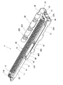
図1は本実施形態のコネクタの全体を示す斜視図、図2はその平面図を示し、両図において、コネクタに取りつけられたグランド板はコネクタの長手方向左半分で図示が省略されている。 FIG. 1 is a perspective view showing the entire connector of the present embodiment, and FIG. 2 is a plan view thereof. In both figures, the ground plate attached to the connector is not shown in the left half of the connector in the longitudinal direction.
このコネクタ1は、回路基板(図示せず)上に配設されるようになっており、図示のごとく左右に長く延びている。このコネクタ1は、コネクタ本体10に選択的にグランド板30が取りつけられて成っている。
The connector 1 is arranged on a circuit board (not shown) and extends long to the left and right as shown. The connector 1 is configured by selectively attaching a
コネクタ本体10は、電気絶縁材料で作られた左右に長く延びるハウジング11の長手方向に位置する両外側面12,13のうちの一方の外側面12の側に複数の端子20が定間隔で植設されている。
The
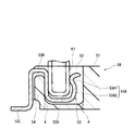
上記ハウジング11は、上記長手方向両端近傍にまで及んで上方に開口する嵌合凹部14が形成されていて、この嵌合凹部14を形成する周壁のうち、上記長手方向に延びる一方の側壁部15に端子20が配列されている。上記嵌合凹部14は、上記長手方向に直角方向である幅方向中央部に位置しており、図2におけるIII-III線断面図を示す図3にも見られるように、ハウジング11に薄い底壁11Aを残す程度まで深く形成されている。上記嵌合凹部14は、図3にて、上方開口14Aの位置から上記底壁11Aの上面たる底部14Bに至る上下範囲で、上記一方の側壁部15側の内側面14Cから没入した収容溝16が端子に対応した位置に形成されている。この収容溝16は、後述の端子の弾性腕部の殆どの部分を収容する没入深さとなっている。上記側壁部15の上端面そして外側面にも、上記収容溝16につながる浅い溝17が形成されている。
The
上記収容溝16そして溝17でハウジング11へ取りつけられる端子20は、金属の細い板帯体を板面に対して屈曲形成されており、その板面に対して直角な面での断面形状が、図3に見られるように、略S字状をなしている。この端子は、逆U字状部分とU字状部分とを連続して有することにより、全体として略S字状をなしている。図3において、端子20は、逆U字状をなす嵌着部21と、これにつながりU字状をなす弾性腕部22と、上記嵌着部21の下端部から延出する接続部23とを有している。
The
上記嵌着部21は、上方から収容溝16へ圧力嵌めされて、端子20をハウジング11に固定保持させる。ハウジング11外で該嵌着部21の下端から横方向に屈曲され延出された接続部23は、ハウジング11の底面と同レベルにあり、コネクタが回路基板上に配されたとき、該回路基板の対応回路部と接面するようになっている。
The
弾性腕部22は、上記収容溝16に嵌着されている上記嵌着部21の下部から屈曲して上方に向け延びており、この部分を可撓とする弾性を有している。この弾性腕部22の上端側たる自由端部は、上記収容溝16外に向け凸状弯曲せられた接触部22Aを有している。この接触部22Aは、上記嵌合凹部14の内部へ向け内側面14Cから若干突出していて、該嵌合凹部14へ相手コネクタが嵌合されたときには、相手コネクタから押圧力を受けて収容溝16の内方へ向け内側面14Cの位置まで弾性変位する。
The
ハウジング外側面部分で上記端子20は嵌着部21が溝17に収められている部分が、該溝17の開口縁よりも若干突出していて、相手コネクタの端子と接触する副接触部21Aを形成し、好ましい形態として、相手コネクタとの接触を確実ならしめかつロックの機能をもたらす突部21A1が形成されている。
The portion of the
上記ハウジング11は、その長手方向両端部に、図2におけるIV-IV線断面を示す図4に見られるようなグランド板取付部11Bを有している。このグランド板取付部11Bに取付けられるグランド板30は、例えば、一枚の金属板を抜き加工そして屈曲加工して作られており、図1、図2にも見られるように、ハウジング11のそれぞれの外側面12,13に沿って位置するグランド本体部31,32と、上記グランド本体部31,32と取付部33とを連結する連結部34,35とを有している。この連結部34,35は、上記ハウジング11の長手方向両端部位置で回路基板に接面するように、グランド板取付部11Bに取りつけられる取付部33の下部と、グランド本体部31,32の下部とで両者を連結している。この実施形態では、連結部35には取付孔36が形成されている。
The
上記グランド本体部31は、ハウジング11の他方の外側面13とほぼ平行な面を有し、上記外側面13との間に間隔を有している。このグランド本体部31の上縁は上記ハウジング11の上面とほぼ同じレベルにあり、上記長手方向両端部においてのみ該グランド本体部31の上縁から上方に弯曲突出部31Aが設けられている。したがって、グランド本体部31の上記上縁は、相手コネクタが嵌合した際に、このグランド本体部31の側で相手コネクタから水平方向に延出するケーブルとは干渉しない。すなわち、上記上縁がハウジング11の上面位置にあるので、その上方位置での上記ケーブルの延出を許容する。しかしながら、グランド板によるシールド効果をさらに向上させるためには、ケーブルが延出する位置でのみ切欠部を形成して、上縁をさらに上方まで、例えば、上記弯曲突部を上記切欠部位置を除いて長手方向全範囲に形成することとしてもよい。
The ground
グランド本体部32は、上記グランド本体部31における場合と同様に、ハウジング11の一方の外側面12とほぼ平行な面を有し、該外側面12との間に間隔を形成している。この間隔は、グランド本体部31の場合の間隔よりも、大きく設定されている。このグランド本体部32とハウジング11の外側面12との間の間隔に、上記端子20の接続部23が位置している。グランド本体部32と取付部33とは、上記長手方向両端部、すなわち同方向で端子不在域で連結部35により連結されているので、グランド本体部32と、取付部33との間は空間をなしていて、上記接続部23は回路基板の対応回路部と接面することが可能となっている。上記グランド本体部32は、その上縁で、内方(ハウジング側)に向けた二種の屈曲部32A.32Bを上記長手方向で交互に有している。一方の屈曲部32Aは幅広で、他方の屈曲部32Bは幅狭である。この他方の屈曲部32Bは、一方の屈曲部32Aよりも内方に向っていて、斜めに延びて弾性舌片を形成し、該弾性舌片は、相手コネクタの嵌合時に、相手グランド板に対して弾圧接触する接触部を形成している。
As in the case of the ground
上記取付部33は、ハウジング11の長手方向両端部に設けられたグランド板取付部11Bに嵌着されるように、図4にみられるごとく、逆U字状をなしている。この逆U字の取付部33の外面は、相手コネクタの対応せる係合部が上方から嵌められて係合する部位ともなっている。このような取付部33は、その両方の肩部外面にロック部を有している。このロック部は突起状をなし、相手コネクタのケーブルが延出する側に位置する主ロック部37Aと、これとは反対側に位置する副ロック部37Bとから成っている。主ロック部37Aの突出量は副ロック部37Bの突出量よりも大きい。すなわち、相手コネクタへの対応ロック部との係合量が、主ロック部37Aの方で大きく設定されている。この突出量の差は、相手コネクタがケーブルをもち上げる力によって外されようとするときに、相手コネクタから受ける力の大きさの差に比例して設定される。
As shown in FIG. 4, the mounting
上記ハウジング11は、他方の外側面13の側で、ハウジング11の長手方向中央位置に、吸着部40を有している。この吸着部40は、コネクタを回路基板上の所定位置へ自動機により実装配置される際に、自動機の吸着部材により吸着される部位を形成し、上面40Aが、ハウジングの上面と同レベル面をなしハウジングの幅方向に突出している。この突出した吸着部40の側面40Bは、記述したグランド本体部31に至近している。上記吸着部40の上面には、上記長手方向両端位置に補助吸着部材の取付けのための取付孔41が形成されている。上記吸着部40の上面40Aのみでは、自動機に対応できないときに、吸着面を拡大するための補助吸着部材を上記取付孔41にて取付ける。吸着部40は相手コネクタの幅範囲内に設けられるのが好ましい。
The
このような本実施形態のコネクタに嵌合される相手コネクタは、図6に示されているように構成される。図6はこの相手コネクタが嵌合された本実施形態のコネクタの使用状態を示す図であり、図6(A)は本実施形態のコネクタがグランド板なしで用いられたとき、図6(B)はグランド板付きとして用いられたときを示す。 The mating connector fitted to the connector of this embodiment is configured as shown in FIG. FIG. 6 is a view showing a usage state of the connector of this embodiment in which the mating connector is fitted. FIG. 6A shows a state in which the connector of this embodiment is used without a ground plate. ) Indicates when used with a ground plate.
図6(A)において、二点鎖線で示されるケーブル付き相手コネクタCの、絶縁体とグランド板C1の一部との間で保持されている同軸ケーブルC2は横方向で右方へ延びている。ケーブルC2の中心導体C3は端子C4に結線されている。該端子は逆U字状部とU字状部とを備え全体として略S字状をなしている。コネクタの外側には上記グランド板C1が取りつけられており、該グランド板C1は、コネクタの上面と、ケーブル延出側の側面を除く外側面とを覆っている。かかる相手コネクタCは、上記端子C4の逆U字状部分の内部に本実施形態のコネクタの端子20を受入れ、端子C4のU字状部分が本実施形態のコネクタの嵌合凹部14へ入り込む。
In FIG. 6A, the coaxial cable C2 held between the insulator and a part of the ground plate C1 of the mating connector C with a cable indicated by a two-dot chain line extends rightward in the lateral direction. . The central conductor C3 of the cable C2 is connected to the terminal C4. The terminal includes an inverted U-shaped portion and a U-shaped portion, and has a substantially S-shape as a whole. The ground plate C1 is attached to the outside of the connector, and the ground plate C1 covers the upper surface of the connector and the outer surface excluding the side surface on the cable extension side. The mating connector C receives the
このような本実施形態のコネクタは、次の要領で使用される。 Such a connector of this embodiment is used in the following manner.
先ず、自動機の吸着部材により、コネクタ1の吸着部40(吸着面40A)にて該コネクタ1を吸着し、これを回路基板上の所定位置へもたらす。しかる後、端子の接続部23が半田により回路基板の対応回路部と接続される。コネクタ1は、グランド板30が取つけられている状態と、グランド板なし(相手グランドを基板に接続させる部分のみ有する)の状態と、いずれでも使用可能である。グランド板30は、コネクタの回路基板への配置の前後のいずれにおいても取付け可能である。グランド板30の使用時には、図4に示される取付孔36にて、半田等により回路基板へ固定しておくとよい。
First, the connector 1 is sucked by the suction member 40 (
次に、図6(A),(B)に見られるように、相手コネクタCをコネクタ1へ嵌合する。相手コネクタCの端子C4は、その逆U字状部分でコネクタ1の端子20をかかえ込むようにして接触する。すなわち、端子C4は、逆U字状部分の一方の直線部でコネクタ1の端子20の副接触部21Aと接触すると共に、対向せる他方の直線部分で接触部22Aを弾圧する。この接触部22Aは弾圧されて収容溝16内へ没する。また、相手コネクタの端子C4のU字状部分は、嵌合凹部14の底部まで進入する。すなわち、この端子C4のU字状部分は、コネクタ1の端子の弾性腕1部22とほぼ同一位置まで下方に進入する。その結果、接触部22Aと接触する上記直線部分は嵌合過程での接触路長が長くなると共に、嵌合時の両コネクタの高さを小さく抑えることができる。
Next, as shown in FIGS. 6A and 6B, the mating connector C is fitted to the connector 1. The terminal C4 of the mating connector C comes into contact with the terminal 20 of the connector 1 at the inverted U-shaped portion. That is, the terminal C4 comes into contact with the
コネクタ1にグランド板30が取付けられているときには、図6(B)に見られるように、グランド本体部31,32がコネクタ1の長手方向に延びる広い範囲で側方から該コネクタ1を覆う。上方では、相手コネクタCのグランド板C1が両コネクタC,1を覆う。コネクタ1のグランド板30は、弾性舌片として形成された接触部32Bが相手コネクタCのグランド板C1と接触しここで互いに導通される。
When the
相手コネクタCから延出するケーブルC2は、グランド本体部31の上縁の上方を経てグランド板と干渉することなく、引き出される。
The cable C <b> 2 extending from the mating connector C is drawn out without interfering with the ground plate through the upper edge of the
相手コネクタCは、図示しないロック部がコネクタ1の突起状のロック部37A,37Bと係合し、コネクタ同士の不用意な抜けが防止される。ケーブルC2が意図しない力を上方に受けたときには、図5に見られるように、該ケーブルC2に近い方のロック部37Aが対向せるロック部37Bに比し大きな力を受ける。しかし、ロック部37Aはロック部37Bよりも係止量が大きいので、上述のような力の配分に応じて適切にコネクタの外れに対坑できる。
In the mating connector C, a lock portion (not shown) is engaged with the projecting
相手コネクタCを離脱の際は、ロック部37B側より治具を用いて行うのが好ましい。又、本発明では、グランド板30の長手方向両端に設けられているが、ハウジング11に設けられても良い。相手コネクタのロック部が相手グランド板に設けられていれば、グランド板30に設けられたロック部37A,37Bと導通し、なお良い。
When the mating connector C is detached, it is preferable to use a jig from the
1 コネクタ 20 端子
11 ハウジング 21 嵌着部
14 嵌合凹部 21A 副接触部
14B 底部 22 弾性接触部
14C 内側面 22A 接触部
16 収容溝 23 接続部
DESCRIPTION OF SYMBOLS 1
14C
16 receiving
Claims (1)
Priority Applications (7)
| Application Number | Priority Date | Filing Date | Title |
|---|---|---|---|
| JP2005307101A JP4563915B2 (en) | 2005-10-21 | 2005-10-21 | Circuit board electrical connector |
| TW095138588A TW200742180A (en) | 2005-10-21 | 2006-10-19 | Electric connector for circuit board |
| EP06812068A EP1950839A1 (en) | 2005-10-21 | 2006-10-20 | Electric connector for circuit board |
| KR1020087010624A KR20080067636A (en) | 2005-10-21 | 2006-10-20 | Electric connector for circuit board |
| CN2006800390877A CN101326686B (en) | 2005-10-21 | 2006-10-20 | Electric connector for circuit board |
| US11/992,652 US7607943B2 (en) | 2005-10-21 | 2006-10-20 | Electric connector for circuit board |
| PCT/JP2006/320900 WO2007046487A1 (en) | 2005-10-21 | 2006-10-20 | Electric connector for circuit board |
Applications Claiming Priority (1)
| Application Number | Priority Date | Filing Date | Title |
|---|---|---|---|
| JP2005307101A JP4563915B2 (en) | 2005-10-21 | 2005-10-21 | Circuit board electrical connector |
Publications (2)
| Publication Number | Publication Date |
|---|---|
| JP2007115576A JP2007115576A (en) | 2007-05-10 |
| JP4563915B2 true JP4563915B2 (en) | 2010-10-20 |
Family
ID=37962580
Family Applications (1)
| Application Number | Title | Priority Date | Filing Date |
|---|---|---|---|
| JP2005307101A Active JP4563915B2 (en) | 2005-10-21 | 2005-10-21 | Circuit board electrical connector |
Country Status (7)
| Country | Link |
|---|---|
| US (1) | US7607943B2 (en) |
| EP (1) | EP1950839A1 (en) |
| JP (1) | JP4563915B2 (en) |
| KR (1) | KR20080067636A (en) |
| CN (1) | CN101326686B (en) |
| TW (1) | TW200742180A (en) |
| WO (1) | WO2007046487A1 (en) |
Families Citing this family (9)
| Publication number | Priority date | Publication date | Assignee | Title |
|---|---|---|---|---|
| JP4889243B2 (en) * | 2005-06-09 | 2012-03-07 | モレックス インコーポレイテド | Connector device |
| JP2009181769A (en) * | 2008-01-30 | 2009-08-13 | Kyocera Elco Corp | Connector, plug connector, and portable terminal |
| KR100896445B1 (en) * | 2009-01-12 | 2009-05-12 | 주식회사 호산테크 | Clip connector |
| JP5250450B2 (en) | 2009-02-27 | 2013-07-31 | 第一電子工業株式会社 | Electrical connector |
| JP5426470B2 (en) * | 2010-05-11 | 2014-02-26 | 株式会社アドバンテスト | Connector and semiconductor test apparatus having the same |
| JP5813349B2 (en) * | 2011-03-29 | 2015-11-17 | 日本航空電子工業株式会社 | Connector and connection object |
| JP6249676B2 (en) * | 2013-08-21 | 2017-12-20 | 宏致電子股▲ふん▼有限公司Aces Electronics Co.,Ltd. | Electrical connector |
| JP6167997B2 (en) * | 2014-06-05 | 2017-07-26 | 株式会社村田製作所 | Connector set and connector |
| JP6269558B2 (en) * | 2014-06-05 | 2018-01-31 | 株式会社村田製作所 | Connector set and connector |
Citations (2)
| Publication number | Priority date | Publication date | Assignee | Title |
|---|---|---|---|---|
| JPH0716381U (en) * | 1993-08-20 | 1995-03-17 | 第一電子工業株式会社 | Electrical connector |
| JPH10162913A (en) * | 1996-11-26 | 1998-06-19 | Matsushita Electric Works Ltd | Connector |
Family Cites Families (16)
| Publication number | Priority date | Publication date | Assignee | Title |
|---|---|---|---|---|
| JP2002008753A (en) * | 2000-06-16 | 2002-01-11 | Matsushita Electric Works Ltd | Connector |
| JP2002319441A (en) * | 2001-04-20 | 2002-10-31 | Jst Mfg Co Ltd | Connecting structure between printed circuit boards |
| JP3682649B2 (en) | 2001-11-27 | 2005-08-10 | 日本航空電子工業株式会社 | Connector device |
| JP3595938B2 (en) * | 2002-01-29 | 2004-12-02 | 日本航空電子工業株式会社 | Surface mount connector and its gauge |
| JP3949064B2 (en) * | 2003-02-06 | 2007-07-25 | ヒロセ電機株式会社 | Electrical connector |
| JP3956920B2 (en) * | 2003-08-26 | 2007-08-08 | 松下電工株式会社 | connector |
| JP2005129255A (en) * | 2003-10-21 | 2005-05-19 | Three M Innovative Properties Co | Connector and connector system |
| US6830478B1 (en) * | 2003-12-10 | 2004-12-14 | Hon Hai Precision Ind. Co., Ltd. | Micro coaxial connector assembly with latching means |
| JP4124760B2 (en) * | 2003-12-22 | 2008-07-23 | モレックス インコーポレーテッド | Coaxial cable connector and cable holder |
| JP2005294034A (en) * | 2004-03-31 | 2005-10-20 | Matsushita Electric Works Ltd | Connector |
| JP2005294036A (en) * | 2004-03-31 | 2005-10-20 | Matsushita Electric Works Ltd | Connector and its manufacturing method |
| CN2785166Y (en) * | 2005-02-01 | 2006-05-31 | 富士康(昆山)电脑接插件有限公司 | Cable connector combination |
| CN2772061Y (en) * | 2005-02-04 | 2006-04-12 | 上海莫仕连接器有限公司 | Electrical connector assembly |
| JP4349633B2 (en) * | 2005-10-21 | 2009-10-21 | ヒロセ電機株式会社 | Circuit board electrical connector |
| JP2008016212A (en) * | 2006-07-03 | 2008-01-24 | I-Pex Co Ltd | Electric connector |
| JP4858050B2 (en) * | 2006-09-29 | 2012-01-18 | オムロン株式会社 | connector |
-
2005
- 2005-10-21 JP JP2005307101A patent/JP4563915B2/en active Active
-
2006
- 2006-10-19 TW TW095138588A patent/TW200742180A/en unknown
- 2006-10-20 EP EP06812068A patent/EP1950839A1/en not_active Withdrawn
- 2006-10-20 KR KR1020087010624A patent/KR20080067636A/en not_active Application Discontinuation
- 2006-10-20 WO PCT/JP2006/320900 patent/WO2007046487A1/en active Application Filing
- 2006-10-20 CN CN2006800390877A patent/CN101326686B/en active Active
- 2006-10-20 US US11/992,652 patent/US7607943B2/en not_active Expired - Fee Related
Patent Citations (2)
| Publication number | Priority date | Publication date | Assignee | Title |
|---|---|---|---|---|
| JPH0716381U (en) * | 1993-08-20 | 1995-03-17 | 第一電子工業株式会社 | Electrical connector |
| JPH10162913A (en) * | 1996-11-26 | 1998-06-19 | Matsushita Electric Works Ltd | Connector |
Also Published As
| Publication number | Publication date |
|---|---|
| TW200742180A (en) | 2007-11-01 |
| US7607943B2 (en) | 2009-10-27 |
| US20090233488A1 (en) | 2009-09-17 |
| WO2007046487A1 (en) | 2007-04-26 |
| EP1950839A1 (en) | 2008-07-30 |
| JP2007115576A (en) | 2007-05-10 |
| CN101326686B (en) | 2011-12-07 |
| CN101326686A (en) | 2008-12-17 |
| KR20080067636A (en) | 2008-07-21 |
| TWI325654B (en) | 2010-06-01 |
Similar Documents
| Publication | Publication Date | Title |
|---|---|---|
| JP4349633B2 (en) | Circuit board electrical connector | |
| JP4563915B2 (en) | Circuit board electrical connector | |
| KR101077462B1 (en) | An electric connector for a circuit board | |
| KR102492103B1 (en) | Connector and connector assembly | |
| US8961215B2 (en) | Electrical connector assembled component, plug connector, and receptacle connector | |
| JP3122168U (en) | Electrical connector | |
| TWI521805B (en) | Electrical connector assembly and socket connector | |
| JP4550733B2 (en) | Electrical connector | |
| US7771236B2 (en) | Electrical connector | |
| US7458822B2 (en) | Electrical connector and combination connector having the same | |
| TW201535879A (en) | Connector | |
| KR20080008250A (en) | Electric connector for flat conductor | |
| KR20120094833A (en) | Electric connector | |
| US8942007B2 (en) | Electrical component | |
| JP2012049015A (en) | Electric connector | |
| TW201401661A (en) | Electrical connector assembly and plug connector | |
| EP1930983A2 (en) | Electrical connector | |
| JP2012049014A (en) | Electric connector | |
| JP2007115579A (en) | Electric connector for circuit board | |
| JP6002636B2 (en) | Flat cable terminal fitting | |
| JP7283971B2 (en) | BOARD CONNECTOR AND BOARD CONNECTOR STRUCTURE | |
| JP2007115578A (en) | Electric connector for circuit board | |
| US8851922B2 (en) | Electrical connector device and connector used in the electrical connector device | |
| KR20130080006A (en) | Electrical connector assembly | |
| CN220797279U (en) | Electric connector and connector assembly |
Legal Events
| Date | Code | Title | Description |
|---|---|---|---|
| A621 | Written request for application examination |
Free format text: JAPANESE INTERMEDIATE CODE: A621 Effective date: 20070626 |
|
| A131 | Notification of reasons for refusal |
Free format text: JAPANESE INTERMEDIATE CODE: A131 Effective date: 20091117 |
|
| A521 | Request for written amendment filed |
Free format text: JAPANESE INTERMEDIATE CODE: A523 Effective date: 20100113 |
|
| TRDD | Decision of grant or rejection written | ||
| A01 | Written decision to grant a patent or to grant a registration (utility model) |
Free format text: JAPANESE INTERMEDIATE CODE: A01 Effective date: 20100727 |
|
| A01 | Written decision to grant a patent or to grant a registration (utility model) |
Free format text: JAPANESE INTERMEDIATE CODE: A01 |
|
| A61 | First payment of annual fees (during grant procedure) |
Free format text: JAPANESE INTERMEDIATE CODE: A61 Effective date: 20100729 |
|
| FPAY | Renewal fee payment (event date is renewal date of database) |
Free format text: PAYMENT UNTIL: 20130806 Year of fee payment: 3 |
|
| R150 | Certificate of patent or registration of utility model |
Ref document number: 4563915 Country of ref document: JP Free format text: JAPANESE INTERMEDIATE CODE: R150 Free format text: JAPANESE INTERMEDIATE CODE: R150 |
|
| FPAY | Renewal fee payment (event date is renewal date of database) |
Free format text: PAYMENT UNTIL: 20130806 Year of fee payment: 3 |
|
| R250 | Receipt of annual fees |
Free format text: JAPANESE INTERMEDIATE CODE: R250 |
|
| R250 | Receipt of annual fees |
Free format text: JAPANESE INTERMEDIATE CODE: R250 |
|
| R250 | Receipt of annual fees |
Free format text: JAPANESE INTERMEDIATE CODE: R250 |
|
| R250 | Receipt of annual fees |
Free format text: JAPANESE INTERMEDIATE CODE: R250 |
|
| R250 | Receipt of annual fees |
Free format text: JAPANESE INTERMEDIATE CODE: R250 |
|
| R250 | Receipt of annual fees |
Free format text: JAPANESE INTERMEDIATE CODE: R250 |
|
| R250 | Receipt of annual fees |
Free format text: JAPANESE INTERMEDIATE CODE: R250 |
|
| R250 | Receipt of annual fees |
Free format text: JAPANESE INTERMEDIATE CODE: R250 |
|
| S531 | Written request for registration of change of domicile |
Free format text: JAPANESE INTERMEDIATE CODE: R313531 |
|
| R350 | Written notification of registration of transfer |
Free format text: JAPANESE INTERMEDIATE CODE: R350 |
|
| R250 | Receipt of annual fees |
Free format text: JAPANESE INTERMEDIATE CODE: R250 |
|
| R250 | Receipt of annual fees |
Free format text: JAPANESE INTERMEDIATE CODE: R250 |
|
| R250 | Receipt of annual fees |
Free format text: JAPANESE INTERMEDIATE CODE: R250 |
|
| R250 | Receipt of annual fees |
Free format text: JAPANESE INTERMEDIATE CODE: R250 |