EP1930983A2 - Electrical connector - Google Patents
Electrical connector Download PDFInfo
- Publication number
- EP1930983A2 EP1930983A2 EP07121912A EP07121912A EP1930983A2 EP 1930983 A2 EP1930983 A2 EP 1930983A2 EP 07121912 A EP07121912 A EP 07121912A EP 07121912 A EP07121912 A EP 07121912A EP 1930983 A2 EP1930983 A2 EP 1930983A2
- Authority
- EP
- European Patent Office
- Prior art keywords
- terminal
- terminal structure
- housing
- structure connector
- connector
- Prior art date
- Legal status (The legal status is an assumption and is not a legal conclusion. Google has not performed a legal analysis and makes no representation as to the accuracy of the status listed.)
- Withdrawn
Links
- 239000002184 metal Substances 0.000 abstract description 6
- 239000000758 substrate Substances 0.000 description 14
- 230000013011 mating Effects 0.000 description 6
- 230000000694 effects Effects 0.000 description 5
- 229910000679 solder Inorganic materials 0.000 description 5
- 238000006073 displacement reaction Methods 0.000 description 4
- 238000005452 bending Methods 0.000 description 1
- 238000004519 manufacturing process Methods 0.000 description 1
- 230000001105 regulatory effect Effects 0.000 description 1
- 238000000926 separation method Methods 0.000 description 1
Images


Classifications
-
- H—ELECTRICITY
- H01—ELECTRIC ELEMENTS
- H01R—ELECTRICALLY-CONDUCTIVE CONNECTIONS; STRUCTURAL ASSOCIATIONS OF A PLURALITY OF MUTUALLY-INSULATED ELECTRICAL CONNECTING ELEMENTS; COUPLING DEVICES; CURRENT COLLECTORS
- H01R12/00—Structural associations of a plurality of mutually-insulated electrical connecting elements, specially adapted for printed circuits, e.g. printed circuit boards [PCB], flat or ribbon cables, or like generally planar structures, e.g. terminal strips, terminal blocks; Coupling devices specially adapted for printed circuits, flat or ribbon cables, or like generally planar structures; Terminals specially adapted for contact with, or insertion into, printed circuits, flat or ribbon cables, or like generally planar structures
- H01R12/50—Fixed connections
- H01R12/51—Fixed connections for rigid printed circuits or like structures
- H01R12/52—Fixed connections for rigid printed circuits or like structures connecting to other rigid printed circuits or like structures
-
- H—ELECTRICITY
- H01—ELECTRIC ELEMENTS
- H01R—ELECTRICALLY-CONDUCTIVE CONNECTIONS; STRUCTURAL ASSOCIATIONS OF A PLURALITY OF MUTUALLY-INSULATED ELECTRICAL CONNECTING ELEMENTS; COUPLING DEVICES; CURRENT COLLECTORS
- H01R12/00—Structural associations of a plurality of mutually-insulated electrical connecting elements, specially adapted for printed circuits, e.g. printed circuit boards [PCB], flat or ribbon cables, or like generally planar structures, e.g. terminal strips, terminal blocks; Coupling devices specially adapted for printed circuits, flat or ribbon cables, or like generally planar structures; Terminals specially adapted for contact with, or insertion into, printed circuits, flat or ribbon cables, or like generally planar structures
- H01R12/50—Fixed connections
- H01R12/51—Fixed connections for rigid printed circuits or like structures
- H01R12/55—Fixed connections for rigid printed circuits or like structures characterised by the terminals
- H01R12/57—Fixed connections for rigid printed circuits or like structures characterised by the terminals surface mounting terminals
-
- H—ELECTRICITY
- H01—ELECTRIC ELEMENTS
- H01R—ELECTRICALLY-CONDUCTIVE CONNECTIONS; STRUCTURAL ASSOCIATIONS OF A PLURALITY OF MUTUALLY-INSULATED ELECTRICAL CONNECTING ELEMENTS; COUPLING DEVICES; CURRENT COLLECTORS
- H01R12/00—Structural associations of a plurality of mutually-insulated electrical connecting elements, specially adapted for printed circuits, e.g. printed circuit boards [PCB], flat or ribbon cables, or like generally planar structures, e.g. terminal strips, terminal blocks; Coupling devices specially adapted for printed circuits, flat or ribbon cables, or like generally planar structures; Terminals specially adapted for contact with, or insertion into, printed circuits, flat or ribbon cables, or like generally planar structures
- H01R12/70—Coupling devices
- H01R12/71—Coupling devices for rigid printing circuits or like structures
- H01R12/712—Coupling devices for rigid printing circuits or like structures co-operating with the surface of the printed circuit or with a coupling device exclusively provided on the surface of the printed circuit
- H01R12/714—Coupling devices for rigid printing circuits or like structures co-operating with the surface of the printed circuit or with a coupling device exclusively provided on the surface of the printed circuit with contacts abutting directly the printed circuit; Button contacts therefore provided on the printed circuit
-
- H—ELECTRICITY
- H01—ELECTRIC ELEMENTS
- H01R—ELECTRICALLY-CONDUCTIVE CONNECTIONS; STRUCTURAL ASSOCIATIONS OF A PLURALITY OF MUTUALLY-INSULATED ELECTRICAL CONNECTING ELEMENTS; COUPLING DEVICES; CURRENT COLLECTORS
- H01R12/00—Structural associations of a plurality of mutually-insulated electrical connecting elements, specially adapted for printed circuits, e.g. printed circuit boards [PCB], flat or ribbon cables, or like generally planar structures, e.g. terminal strips, terminal blocks; Coupling devices specially adapted for printed circuits, flat or ribbon cables, or like generally planar structures; Terminals specially adapted for contact with, or insertion into, printed circuits, flat or ribbon cables, or like generally planar structures
- H01R12/70—Coupling devices
- H01R12/71—Coupling devices for rigid printing circuits or like structures
- H01R12/712—Coupling devices for rigid printing circuits or like structures co-operating with the surface of the printed circuit or with a coupling device exclusively provided on the surface of the printed circuit
- H01R12/716—Coupling device provided on the PCB
-
- H—ELECTRICITY
- H01—ELECTRIC ELEMENTS
- H01R—ELECTRICALLY-CONDUCTIVE CONNECTIONS; STRUCTURAL ASSOCIATIONS OF A PLURALITY OF MUTUALLY-INSULATED ELECTRICAL CONNECTING ELEMENTS; COUPLING DEVICES; CURRENT COLLECTORS
- H01R13/00—Details of coupling devices of the kinds covered by groups H01R12/70 or H01R24/00 - H01R33/00
- H01R13/648—Protective earth or shield arrangements on coupling devices, e.g. anti-static shielding
- H01R13/658—High frequency shielding arrangements, e.g. against EMI [Electro-Magnetic Interference] or EMP [Electro-Magnetic Pulse]
- H01R13/6581—Shield structure
- H01R13/6582—Shield structure with resilient means for engaging mating connector
- H01R13/6583—Shield structure with resilient means for engaging mating connector with separate conductive resilient members between mating shield members
Definitions
- the present invention relates to an electrical connector to fit to each other.
- An electrical connector is provided with a plurality of terminals maintaining a flat plate surface of a metal sheet and arranged in a housing in a plate thickness direction thereof.
- the connector in Patent Reference has been known.
- a pair of connectors to fit into each other has the flat terminals described above.
- An outer dimension of such a terminal in an arrangement direction thereof is equal to a plate thickness dimension; and therefore, the terminal is thin. Accordingly, a plurality of such terminals may be arranged in a high,density.
- the terminal of the both connectors has a plane shape having an S-shape portion. Further, when the connectors are fitted into each other, the terminals are adjacent to an edge surface on a free edge side of the S-shape portion or a surface of a plate thickness width thereof.
- the S-shape portion is elastic inside of the plane described above because of the shape, and contacts through an elastic contact. An elastic force applied to the terminals through the elastic contact influences on a sidewall of the housing at a right angle.
- the sidewall of the housing holds the terminals and extends long in an arrangement direction with respect to the terminals.
- One of two bend portions provided at the S-shape portion fits into the sidewall. The sidewall is not that much made thick.
- the terminals of the connectors are arranged in two rows to face with each other. Accordingly, the terminals generate a symmetrical elastic pressure force. Further, the elastic pressure force is applied in a direction to divide the sidewalls of the housing.
- the terminals are made to be in the S-shape to maintain the plane of the metal sheet. Edge surfaces of the S-shape portion elastically contact with each other, which causes some flaws.
- a dimension of the terminal in an arrangement direction thereof is a plate thickness. That is, the terminal is made thin. Since a large number of the terminals are arranged, the sidewall of the housing becomes long. The sidewall of the housing is made relatively thin and forces applied from all the terminals to the sidewall are combined to be large because of the number of the terminals. Accordingly, the sidewall tends to be bent outwardly. An amount of bending is the largest in a center position in the arrangement direction thereof. Accordingly, a contact pressure with a mating connector may vary depending on a position in the arrangement direction with respect to the terminal. Consequently, a strength of the terminal on the sidewall or a variance of the contact pressure among the terminals may be an issue.
- the terminal is contacted to the mating connector within a plate thickness. Accordingly, when there is a variation made at a production or there is a displacement upon fitting in a position of the terminal in an arrangement direction or in a plate thickness direction thereof, the terminal and the mating terminal contact each other in a small surface. The reduction in the contact area is not preferred because an electric resistance is increased and a signal is deteriorated. The displacement may occur when the terminal fits into the mating connector in a twisted state. Further, when the displacement is great, the terminal may be possibly shortcircuited with an adjacent terminal through the mating terminal.
- the terminal is enlarged in a fitting direction with respect to the connector to maintain enough elasticity in the S-shape portion thereof. Accordingly, the connector may be enlarged in the direction.
- This type of the connector is often arranged on a substrate to connect the substrates. Accordingly, the connector is preferred to be small and a low profile, which may not be satisfied by the conventional connector.
- An object of the present invention is to provide a low profile electrical connector capable of preventing an overload to a sidewall of a housing and obtaining a stable contact.
- an electrical connector includes a plurality of terminals made of a metal sheet and arranged in a housing in a plate thickness direction thereof to face with each other in plate surfaces. Further, the terminals are fitted into each other on a fitting surface provided on the housing.
- a female terminal structure connector and a male terminal structure connector constitute a pair of the electrical connectors.
- the terminal of the connectors extends in a direction perpendicular to a fitting surface.
- a part of the terminal situated on a fitting surface side has a contact portion in a plate surface parallel to a fitting direction thereof.
- the terminal of at least one of the connectors has an elastic portion to elastically bend in a plate thickness direction in a part of the terminal. The contact portion is provided in the elastic portion.
- the terminals of the connectors when a pair of the connectors fits into each other, the terminals of the connectors become adjacent to each other in a width direction (fitting direction) in a direction parallel to a plate surface of the terminals, and the plate surface thereof contacts each other.
- the terminal of at least one of the connectors has an elastic pressure in a plate thickness direction thereof. Accordingly, the contact portions of the terminals of the both connectors elastically contact with the plate surfaces in a plate thickness direction thereof. As a result, even though the contact portions are somewhat displaced from a regular position in a fitting direction with respect to the connector, there is no effect because the plate surfaces of the contact portions are large enough to maintain enough contact area.
- the connector according to the present invention has the terminal having a small plate thickness in an arrangement direction with respect to the terminal. Accordingly, the connector is small. Further, a width of the terminal in a fitting direction thereof does not have to be large, and the connector may be small in the direction.
- a total force of elastic contact forces applied to a plurality of the terminals influences on an edge wall of the housing in an arrangement direction with respect to the terminal. Accordingly, little deformation of the edge wall that is relatively short occurs. Therefore, the sidewall that is long in an arrangement direction with respect to the terminal has no influence from the terminal, and the sidewall may not be bent. Accordingly, there are no fluctuations in the contact pressure among a plurality of the terminals.
- a pair of the connectors comprises the male terminal structure connector and the female terminal structure connector.
- the male terminal structure connector has the contact portion protruding from a fitting surface of the housing.
- the female terminal structure connector is situated inside of the receiving recess portion.
- the receiving recess portion is recessed from the fitting portion.
- the connectors may be formed so that the contact portion of the male terminal structure connector may enter the receiving recess portion.
- the contact portion of the terminal of the male terminal structure connector may be accommodated.
- the contact portion of the terminal of the male terminal structure connector may be designed to contact an inner wall surface of the receiving recess portion to be supported without a bend of a plate surface or to contact an inner wall surface of the receiving recess portion to be supported when the plate surface receives an elastic pressure from the mating female terminal structure connector to bend no more than a defined amount.
- the plate surface may be bent or provided with a space with the inner wall surface. In any case, the contact portions of the terminal of the connectors contact each other to bend within the receiving recess portion. Accordingly, the terminal does not contact an adjacent terminal no matter how much the contact portion is bent.
- the terminal of the female terminal structure connector has an elastic portion.
- the elastic portion is the contact portion on the free edge of the terminal that keeps a specific distance from the inner wall surface of the receiving recess portion. Accordingly, the elastic portion that is the contact portion of the terminal of the female terminal structure connector is bent inside of the receiving recess portion. Further, a position of the contact portion of the terminal of the male terminal structure connector may be regulated in a plate thickness direction thereof inside of the inner wall surface of the receiving recess portion.
- the terminal of the male terminal structure connector may be made so that the contact portion is an elastic portion on an edge portion.
- the connection portion that is connected to a circuit surface of the substrate is provided on an edge of the terminal. Further, the connection portion may protrude from the opening portion and engage with the circuit surface. Accordingly, the approximate entire connector may be accommodated inside of the opening portion of the substrate and only the connection portion of the terminal may be exposed on a circuit surface of the substrate. Therefore, the connector may be produced to have a low profile. In this case, the connection portion of the male terminal structure connector engages with the circuit surface of the substrate situated on a receiving side of the female terminal structure connector.
- connection portion of one of the male terminal structure connector and the female terminal structure connector may be exposed from a bottom surface of the housing on an opposite side of the receiving side of each other. Accordingly, the connector may be placed on the circuit surface of the substrate or a flat cable and connected with the circuit surface with solder or the like.
- the male terminal structure connector may be covered with a shield plate on an opposite side of the receiving side for the female terminal structure connector. Accordingly, the male terminal structure connector may obtain a shield effect when the male terminal structure connector is accommodated inside of the corresponding opening portion.
- the shield plate covers the female terminal structure connector. Accordingly, the both connectors obtain the shield effect.
- a portion of the shield plate may be supported on the substrate surface. Further, the shield plate may be accommodated within the substrate thickness.
- the terminal made of a metal sheet is provided to extend in a direction perpendicular to the fitting surface with respect to the housing. Further, when the connectors fit into each other, the terminals contact with each other in the contact portions provided on the plate surfaces in a plate thickness direction thereof. Accordingly, no force is applied to the sidewall of the housing from the terminal upon fitting the connectors.
- the sidewall of the housing extends long in an arrangement direction with respect to the terminals.
- the contact portion provided in the plate surface has a relatively large area. Accordingly, the terminals have an enough contact area and may transmit a stable signal regardless of a little positional displacement of the terminals. Further, the size of the terminal may be kept small in a fitting direction thereof; therefore, the connector may have a low profile in the direction.
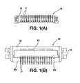
- Figs. 1(A) and 1(B) are plan views showing a pair of electrical connectors according to an embodiment of the present invention.
- Fig. 1(A) is a plan view showing a female terminal structure connector 10
- Fig. 1(B) is a plan view showing a male terminal structure connector 20.
- the female terminal structure connector 10 is provided with a plurality of terminals 11.
- a plurality of the terminals 11 having a plate shape and made of a metal sheet is arranged on a housing 12 in a plate thickness direction or a direction perpendicular to a plate surface thereof.
- the male terminal structure connector 20 is provided with a receiving recess portion 23 to receive the female terminal structure connector 10.
- the receiving recess portion 23 is provided in a housing 22 to pass through as a window. Further, a plurality of terminals 21 having a plate shape is arranged along one of sidewalls 22A provided in the housing 22 in a plate thickness direction or a direction perpendicular to a plate surface thereof. An inner wall surface of the receiving recess portion 23 constitutes a fitting surface 23A having an appropriate shape and size to fit to the female terminal structure connector 10.
- the male terminal structure connector 20 is provided with clamps 34 to attach the male terminal structure connector 20 to a substrate (not shown). The clamps 34 extend outside of the housing 22 from both ends thereof in an arrangement direction of the terminals.
- Figs. 2(A) and 2(B) are sectional views showing the pair of electrical connectors according to the embodiment of the present invention.
- Fig. 2(A) is a sectional view showing a state before the electrical connectors are fitted
- Fig. 2(B) is a sectional view showing a state after the electrical connectors are fitted
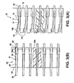
- Figs. 3(A) and 3(B) are enlarged views showing the pair of electrical connectors according to the embodiment of the present invention.
- Fig. 3(A) is an enlarged view showing the female terminal structure connector 10
- Fig. 3(B) is an enlarged view showing the male terminal structure connector 20.
- the terminals 11 having a flat plate surface parallel to a sheet surface are arranged on the housing 12 in the female terminal structure connector 10. Further, the terminals 11 are arranged at a specific pitch in a perpendicular direction with respect to the sheet surface.
- the terminal 11 comprises a connection portion 13, a contact portion 14, a joining portion 15, and a fixed portion 16.
- the connection portion 13 connects the terminal 11 and a flexible circuit board P1 or a circuit portion of the substrate with solder.
- the contact portion 14 is provided to contact with the terminals 21 of the male terminal structure connector 20.
- the joining portion 15 connects the connection portion 13 and the contact portion 14.
- the fixed portion 16 is provided to fix the terminals 11 to the housing 12.
- connection portion 13 and the joining portion 15 of the terminal 11 are situated so that top edges of the connection portion 13 and the joining portion 15 slightly protrude upwardly from the housing 12 to contact with the flexible circuit board P1.
- the joining portion 15 has a slight slope in a left portion that is closer to the corresponding terminal 21 of the male terminal structure connector 20.
- the terminal 11 does not require the slope, and the portion may be a plane.
- the contact portion 14 is provided to extend downwardly on a left edge. Further, as shown in Figs. 5(A) to 5(D) , the contact protrusion portion 14A is provided to protrude upwardly in a plate thickness direction thereof to be closer to the corresponding terminal 21 on a lower edge side of the contact portion 14.
- the connection portion 13 extends to a right side in Fig. 2(A) to be situated outside of the housing 12.
- the fixed portion 16 extends downwardly from a border of the joining portion 15 and the connection portion 13. Further, the protrusion 16A having a nail-like shape is provided on a side edge of the fixed portion 16 for fixing.
- the housing 12 of the female terminal structure connector 10 is provided with a receiving groove 17 and a fixed groove 18 as shown in Fig. 2(A) .
- the receiving groove 17 is provided to open upwardly, and the joining portion 15 and the connection portion 13 fit into the receiving groove 17 from above.
- the fixed groove 18 is provided to pass through downwardly. Further, the fixed portion 16 communicates with the receiving groove 17 and is pressed into the fixed groove 18.
- the housing 12 has a receiving recess portion 19 having a space in a plate thickness direction with respect to the contact portion 14 of the terminal 11 as shown in Fig. 3(A) .
- the receiving recess portion 19 allows the contact portion of the terminal 21 of the male terminal structure connector 20 to enter while communicating with a space formed with respect to a slope portion on a left edge of the joining portion 15.
- a deformation is allowed only in a range covering from the slope portion to the contact portion 14.
- the female terminal structure connector 10 is attached to the flexible circuit board P1, and the connection portion 13 is connected to the corresponding circuit portion with solder.
- the male terminal structure connector 20 fits into the female terminal structure connector 10. Similar to the female terminal structure connector 10, a plurality of the terminals 21 having a plate shape and made of a sheet plate is arranged in the housing 22 in a plate thickness direction or a direction perpendicular to a plate surface thereof. As shown in Figs. 1(B) and 2(A) , the terminals 21 are provided on the sidewall 22A, one of the surrounding walls of the housing that is provided with the receiving recess portion 23 having the fitting surface 23A for the female terminal structure connector 10.
- the terminal 21 has a flat plate surface parallel to a sheet surface.
- the terminal 21 comprises a connection portion 24, a contact portion 25, a joining portion 26, and a fixed portion 27.
- the connection portion 24 is situated on a surface of a corresponding circuit of a circuit board P2 outside of an opening portion P2-A when the opening portion P2-A of the circuit board P2 accommodates the male terminal structure connector 20.
- the contact portion 25 contacts with the contact portion 14 of the terminal 11 of the female terminal structure connector 10.
- the joining portion 26 connects the contact portion 25 and the connection portion 24.
- the fixed portion 27 is provided to fix the terminal 21 to the housing 22.
- the joining portion 26 has a step portion 26A on an upper edge in a position corresponding with the fixed portion 27 in a vertical direction thereof.
- a left side of the step 26A is flush with an upper edge of the connection portion 24.
- a right side of the step portion 26A is buried to be flush with an upper face of the circuit board P2 so that an edge of the flexible circuit board P1 connected to the female terminal structure connector 10 is accommodated.
- the contact portion 25 extends downwardly in a leg shape.
- a top edge of the contact portion 25 is formed to be a taper edge 25A to support an engagement with the contact portion 14 of the terminal 11 of the female terminal structure connector 10.
- the contact portion 25 includes an engagement protrusion portion 25B to engage with the contact portion 14 at a specific fitting position (shown in Figs. 5(A) to 5(D) ).
- the fixed portion 27 extends downwardly parallel to the contact portion 25 in a leg shape as shown in Fig. 2(A) , and a protrusion 27A having a nail-like shape is provided on a side edge thereof for fixing.
- the contact portion 25 and the fixed portion 27 extend no more-than a thickness of the circuit board P2.
- the housing 22 of the male terminal structure connector 20 includes a receiving groove 28 and a fixed groove 29.
- the receiving groove 28 is formed to be open upwardly to receive a part of the joining portion 26 and the connection portion 24 from above.
- the fixed groove 29 is communicated with the receiving groove 28 and provided to pass through downwardly, so that the fixed portion 27 of the terminal 21 is pressed into the fixed groove 29.
- the housing 22 has a recess portion 30 open to the receiving recess portion 23 as shown in Fig. 3(B) .
- the recess portion 30 has a space against the contact portion 25 of the terminal 21 in a thickness direction with respect to the contact portion 25. Accordingly, the contact portion 25 is elastic in the thickness direction thereof and may be elastically deformed inside of the recess portion 30.
- the recess portion 30 has a depth in a horizontal direction thereof in Fig. 2(A) , so that a right portion of the contact portion 25 protrudes from the recess portion 30.
- the male terminal structure connector 20 is accommodated in the opening portion P2A of the circuit board P2.
- the connection portion 24 of the terminal 21 is situated outside of the opening portion P2A of the circuit board P2 in a thickness direction of the circuit board, and a lower edge of the connection portion 24 is situated on a corresponding circuit portion of the circuit board P2.
- the connection portion 24 is connected with the corresponding circuit portion with solder.
- the female terminal structure connector 10 and the male terminal structure connector 20 described above are connected as described below.
- the female terminal structure connector 10 is situated above the male terminal structure connector 20.
- the female terminal structure connector 10 is attached and connected to the flexible circuit board P1, and the male terminal structure connector 20 is accommodated to the opening portion P2A of the circuit board P2 to be connected to the circuit board P2.
- Plan views of the female terminal structure connector 10 and the male terminal structure connector 20 when the flexible circuit board P1 and the circuit board P2 are omitted are shown in Figs. 3(A) and 3(B) , respectively.
- the female terminal structure connector 10 is pulled down and accommodated in the receiving recess portion 23 of the male terminal structure connector 20.
- the contact portion 25 enters the receiving recess portion 19 of the female terminal structure connector 10.
- the contact portion 25 of the male terminal structure connector 20 is guided along or is adjacent to one of the inner wall surfaces of the receiving recess portion 19 situated on a contact protrusion portion 14A side of the contact portion 14 of the female terminal structure connector 10.
- the contact portion 25 of the male terminal structure connector 20 enters between the inner wall surface and the contact protrusion portion 14A to press the contact portion 14 in the contact protrusion portion 14A, thereby generating an elastic flexure in a plate thickness direction of the contact portion 14. Accordingly, a contact pressure is generated between the contact portions 25 and 14 as shown in Figs. 4 and 5(A) to 5(D) .
- the contact protrusion portion 14A of the terminal 11 of the female terminal structure connector 10 engages with the engagement protrusion portion 25B of the terminal 21 of the male terminal structure connector 20 as shown in Fig. 5(D) . Accordingly, a fitting of the connectors to a specific fitting position may be confirmed with a click, and a separation of the connectors may be prevented.
- the terminals 11 and 21 of the connectors 10 and 20 have the contact pressure at the contact portions 14 and 25 in a plate thickness direction of the terminals.
- the contact portion 25 of the male terminal structure connector 20 is supported in or is adjacent to one of the inner wall surfaces of the receiving recess portion 19 of the female terminal structure connector 10.
- the contact portion 14 of the female terminal structure connector 10 is elastically deformed and is supported in or is adjacent to the other inner wall surface of the receiving recess portion 19 as shown in Fig. 4 .
- the terminals 11 and 21 of the female terminal structure connector 10 and the male terminal structure connector 20 are connected through the contact pressure.
- the contact portion 25 of the terminal 21 of the male terminal structure connector 20 has a space with the inner wall surface of the recess portion 30 inside the recess portion 30 of the male terminal structure connector 20, and may be elastically bent. Accordingly, the terminals is provided with a floating effect (following deformation).
- Figs. 6(A) and 6(B) are enlarged plan views showing an essential portion of the pair of electrical connectors according to the embodiment of the present invention.
- Fig. 6(A) is a plan view showing a state before the electrical connectors are fitted
- Fig. 6(B) is a plan view showing a state after the electrical connectors are fitted.
- a taper portion 19A having a width of ⁇ 2 larger than ⁇ 1 is provided on a lower surface or a fitting side of the receiving recess portion 19 of the female terminal structure connector 10. Accordingly, when the contact portion 25 of the terminal 21 of the male terminal structure connector 20 is displaced to a position in which the contact portion 25 interferes for ⁇ 1 against the inner wall surface of the receiving recess portion 19 provided in the housing of female terminal structure connector 10, the contact portion 25 of the male terminal structure connector 20 is led by the taper portion 19A of the female terminal structure connector 10 to enter the receiving recess portion 19 and contacts with the contact portion 14 of the terminal 11 of the female terminal structure connector 10 as shown in Fig. 6(B) . Accordingly, the contact portion 25 of the male terminal structure connector 20 can be elastically bent to obtain the floating effect within the range of ⁇ 2 .
- the present invention is not limited to the embodiments shown in Figs. 1(A)-1(B) to 6(A)-6(B) .
- the male terminal structure connector may not be accommodated to the opening portion of the substrate.
- the male terminal structure connector may be arranged on and connected to the substrate.
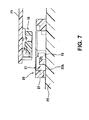
- Fig. 7 is a sectional view showing a pair of electrical connectors in a state before the electrical connectors are fitted according to another embodiment of the present invention.
- the terminal 21 of the male terminal structure connector 20 extends so that a lower edge of the fixed portion 27 is adjacent to a surface of the circuit board P2. Accordingly, the lower edge forms a connection portion 37A.
- connection portion 37A is connected to a corresponding circuit portion of the circuit board P2 with solder.
- Fig. 8 is a sectional view showing electrical connectors in a state after the electrical connectors are fitted according to a further embodiment of the present invention.
- the male terminal structure connector 20 has a shield plate 31.
- the shield plate 31 having a U-shape section covers the male terminal structure connector 20 from below.
- An inner surface of the shield 31 is provided with an insulative layer 31A to prevent a short circuit of the terminal 21 and the shield plate 31.
- the shield plate 31 may be attached to the housing 22. Further, a flange portion (not shown) extending from a top edge of the sidewall in a perpendicular direction with respect to a sheet surface may engage with a top edge of the opening portion of the substrate.
Abstract
The terminals are fitted into each other on a fitting surface (23A) provided on the housing (12,22). In the electrical connector, the terminal (11,21) extends in a direction perpendicular to a fitting surface (23A). A part of the terminal (11,21) situated on a fitting surface (23A) side has a contact portion (14,25) in a plate surface parallel to a fitting direction thereof. Further, the terminal (11,21) of at least one of the connectors (10,20) has an elastic portion to elastically bend in a plate thickness direction in a part of the terminal (11,21). The contact portion (14,25) is provided in the elastic portion.

Description
- The present invention relates to an electrical connector to fit to each other.
- An electrical connector is provided with a plurality of terminals maintaining a flat plate surface of a metal sheet and arranged in a housing in a plate thickness direction thereof. For example, the connector in Patent Reference has been known.
- In Patent Reference, a pair of connectors to fit into each other has the flat terminals described above. An outer dimension of such a terminal in an arrangement direction thereof is equal to a plate thickness dimension; and therefore, the terminal is thin. Accordingly, a plurality of such terminals may be arranged in a high,density.
- The terminal of the both connectors has a plane shape having an S-shape portion. Further, when the connectors are fitted into each other, the terminals are adjacent to an edge surface on a free edge side of the S-shape portion or a surface of a plate thickness width thereof. The S-shape portion is elastic inside of the plane described above because of the shape, and contacts through an elastic contact. An elastic force applied to the terminals through the elastic contact influences on a sidewall of the housing at a right angle. The sidewall of the housing holds the terminals and extends long in an arrangement direction with respect to the terminals. One of two bend portions provided at the S-shape portion fits into the sidewall. The sidewall is not that much made thick.
- In Patent Reference, the terminals of the connectors are arranged in two rows to face with each other. Accordingly, the terminals generate a symmetrical elastic pressure force.
Further, the elastic pressure force is applied in a direction to divide the sidewalls of the housing.
Patent Reference;Japanese Patent Publication No. 2004-241253 - In the connector of Patent Reference 1, the terminals are made to be in the S-shape to maintain the plane of the metal sheet. Edge surfaces of the S-shape portion elastically contact with each other, which causes some flaws.
- First, a dimension of the terminal in an arrangement direction thereof is a plate thickness. That is, the terminal is made thin. Since a large number of the terminals are arranged, the sidewall of the housing becomes long. The sidewall of the housing is made relatively thin and forces applied from all the terminals to the sidewall are combined to be large because of the number of the terminals. Accordingly, the sidewall tends to be bent outwardly. An amount of bending is the largest in a center position in the arrangement direction thereof. Accordingly, a contact pressure with a mating connector may vary depending on a position in the arrangement direction with respect to the terminal. Consequently, a strength of the terminal on the sidewall or a variance of the contact pressure among the terminals may be an issue.
- Further, the terminal is contacted to the mating connector within a plate thickness. Accordingly, when there is a variation made at a production or there is a displacement upon fitting in a position of the terminal in an arrangement direction or in a plate thickness direction thereof, the terminal and the mating terminal contact each other in a small surface. The reduction in the contact area is not preferred because an electric resistance is increased and a signal is deteriorated. The displacement may occur when the terminal fits into the mating connector in a twisted state. Further, when the displacement is great, the terminal may be possibly shortcircuited with an adjacent terminal through the mating terminal.
- Further, the terminal is enlarged in a fitting direction with respect to the connector to maintain enough elasticity in the S-shape portion thereof. Accordingly, the connector may be enlarged in the direction. This type of the connector is often arranged on a substrate to connect the substrates. Accordingly, the connector is preferred to be small and a low profile, which may not be satisfied by the conventional connector.
- The present invention is made in consideration of the problem described above. An object of the present invention is to provide a low profile electrical connector capable of preventing an overload to a sidewall of a housing and obtaining a stable contact.
- The above object is achieved by the invention recited in claim 1.
- In order to attain the objects described above, according to an embodiment of the present invention, an electrical connector includes a plurality of terminals made of a metal sheet and arranged in a housing in a plate thickness direction thereof to face with each other in plate surfaces. Further, the terminals are fitted into each other on a fitting surface provided on the housing. A female terminal structure connector and a male terminal structure connector constitute a pair of the electrical connectors.
- In the pair of the electrical connectors of the present invention, the terminal of the connectors extends in a direction perpendicular to a fitting surface. A part of the terminal situated on a fitting surface side has a contact portion in a plate surface parallel to a fitting direction thereof. Further, the terminal of at least one of the connectors has an elastic portion to elastically bend in a plate thickness direction in a part of the terminal. The contact portion is provided in the elastic portion.
- According to the present invention, when a pair of the connectors fits into each other, the terminals of the connectors become adjacent to each other in a width direction (fitting direction) in a direction parallel to a plate surface of the terminals, and the plate surface thereof contacts each other. At this time, the terminal of at least one of the connectors has an elastic pressure in a plate thickness direction thereof. Accordingly, the contact portions of the terminals of the both connectors elastically contact with the plate surfaces in a plate thickness direction thereof. As a result, even though the contact portions are somewhat displaced from a regular position in a fitting direction with respect to the connector, there is no effect because the plate surfaces of the contact portions are large enough to maintain enough contact area.
- The connector according to the present invention has the terminal having a small plate thickness in an arrangement direction with respect to the terminal. Accordingly, the connector is small. Further, a width of the terminal in a fitting direction thereof does not have to be large, and the connector may be small in the direction. A total force of elastic contact forces applied to a plurality of the terminals influences on an edge wall of the housing in an arrangement direction with respect to the terminal. Accordingly, little deformation of the edge wall that is relatively short occurs. Therefore, the sidewall that is long in an arrangement direction with respect to the terminal has no influence from the terminal, and the sidewall may not be bent. Accordingly, there are no fluctuations in the contact pressure among a plurality of the terminals.
- In the present invention, a pair of the connectors comprises the male terminal structure connector and the female terminal structure connector. The male terminal structure connector has the contact portion protruding from a fitting surface of the housing. The female terminal structure connector is situated inside of the receiving recess portion. The receiving recess portion is recessed from the fitting portion. The connectors may be formed so that the contact portion of the male terminal structure connector may enter the receiving recess portion.
- In the receiving recess portion, the contact portion of the terminal of the male terminal structure connector may be accommodated. The contact portion of the terminal of the male terminal structure connector may be designed to contact an inner wall surface of the receiving recess portion to be supported without a bend of a plate surface or to contact an inner wall surface of the receiving recess portion to be supported when the plate surface receives an elastic pressure from the mating female terminal structure connector to bend no more than a defined amount. Further, the plate surface may be bent or provided with a space with the inner wall surface. In any case, the contact portions of the terminal of the connectors contact each other to bend within the receiving recess portion. Accordingly, the terminal does not contact an adjacent terminal no matter how much the contact portion is bent.
- In the present invention, the terminal of the female terminal structure connector has an elastic portion. The elastic portion is the contact portion on the free edge of the terminal that keeps a specific distance from the inner wall surface of the receiving recess portion. Accordingly, the elastic portion that is the contact portion of the terminal of the female terminal structure connector is bent inside of the receiving recess portion. Further, a position of the contact portion of the terminal of the male terminal structure connector may be regulated in a plate thickness direction thereof inside of the inner wall surface of the receiving recess portion.
- Further, the terminal of the male terminal structure connector may be made so that the contact portion is an elastic portion on an edge portion.
- In the present invention, when the male terminal structure connector is situated inside of the corresponding opening portion, the connection portion that is connected to a circuit surface of the substrate is provided on an edge of the terminal. Further, the connection portion may protrude from the opening portion and engage with the circuit surface. Accordingly, the approximate entire connector may be accommodated inside of the opening portion of the substrate and only the connection portion of the terminal may be exposed on a circuit surface of the substrate. Therefore, the connector may be produced to have a low profile. In this case, the connection portion of the male terminal structure connector engages with the circuit surface of the substrate situated on a receiving side of the female terminal structure connector.
- In the present invention, the connection portion of one of the male terminal structure connector and the female terminal structure connector may be exposed from a bottom surface of the housing on an opposite side of the receiving side of each other. Accordingly, the connector may be placed on the circuit surface of the substrate or a flat cable and connected with the circuit surface with solder or the like.
- In the present invention, the male terminal structure connector may be covered with a shield plate on an opposite side of the receiving side for the female terminal structure connector. Accordingly, the male terminal structure connector may obtain a shield effect when the male terminal structure connector is accommodated inside of the corresponding opening portion. When the female terminal structure connector is accommodated inside of the male terminal structure connector, the shield plate covers the female terminal structure connector.
Accordingly, the both connectors obtain the shield effect. A portion of the shield plate may be supported on the substrate surface. Further, the shield plate may be accommodated within the substrate thickness. - In the present invention, as described above, the terminal made of a metal sheet is provided to extend in a direction perpendicular to the fitting surface with respect to the housing. Further, when the connectors fit into each other, the terminals contact with each other in the contact portions provided on the plate surfaces in a plate thickness direction thereof. Accordingly, no force is applied to the sidewall of the housing from the terminal upon fitting the connectors. The sidewall of the housing extends long in an arrangement direction with respect to the terminals.
- Further, a deformation of the sidewall of the housing or a fluctuation of the contact pressure in the terminals does not occur. In addition, the contact portion provided in the plate surface has a relatively large area. Accordingly, the terminals have an enough contact area and may transmit a stable signal regardless of a little positional displacement of the terminals. Further, the size of the terminal may be kept small in a fitting direction thereof; therefore, the connector may have a low profile in the direction.
- Embodiments of the invention will now be described by way of example with respect to the accompanying drawings, in which:
-
Figs. 1(A) and 1(B) are plan views showing a pair of electrical connectors according to an embodiment of the present invention, whereinFig. 1(A) is a plan view showing a female terminal structure connector andFig. 1(B) is a plan view showing a male terminal structure connector; -
Figs. 2(A) and 2(B) are sectional views showing the pair of electrical connectors according to the embodiment of the present invention, whereinFig. 2(A) is a sectional view showing a state before the electrical connectors are fitted andFig. 2(B) is a sectional view showing a state after the electrical connectors are fitted; -
Figs. 3(A) and 3(B) are enlarged views showing the pair of electrical connectors according to the embodiment of the present invention, whereinFig. 3(A) is an enlarged view showing the female terminal structure connector andFig. 3(B) is an enlarged view showing the male terminal structure connector; -
Fig. 4 is a plan view showing the pair of electrical connectors in a fitted state according to the embodiment of the present invention; -
Figs. 5(A) to 5(D) are sectional views showing terminals of the electrical connectors according to the embodiment of the present invention, whereinFig. 5(A) is a sectional view showing a state before the electrical connectors are fitted,Fig. 5(B) is a sectional view showing a state that the electrical connectors start being fitted,Fig. 5(C) is a sectional view showing a state during the electrical connectors are fitted, andFig. 5(D) is a sectional view showing a state after the electrical connectors are fitted; -
Figs. 6(A) and 6(B) are enlarged plan views showing an essential portion of the pair of electrical connectors according to the embodiment of the present invention, whereinFig. 6(A) is a plan view showing a state before the electrical connectors are fitted andFig. 6(B) is a plan view showing a state after the electrical connectors are fitted; -
Fig. 7 is a sectional view showing a pair of electrical connectors in a state before the electrical connectors are fitted according to another embodiment of the present invention; and -
Fig. 8 is a sectional view showing a pair of electrical connectors in a state after the electrical connectors are fitted according to a further embodiment of the present invention. - Hereunder, embodiments of the present invention will be explained with reference to the accompanying drawings.
-
Figs. 1(A) and 1(B) are plan views showing a pair of electrical connectors according to an embodiment of the present invention.Fig. 1(A) is a plan view showing a femaleterminal structure connector 10 andFig. 1(B) is a plan view showing a maleterminal structure connector 20. - As shown in
Fig. 1(A) , the femaleterminal structure connector 10 is provided with a plurality ofterminals 11. A plurality of theterminals 11 having a plate shape and made of a metal sheet is arranged on ahousing 12 in a plate thickness direction or a direction perpendicular to a plate surface thereof. The maleterminal structure connector 20 is provided with a receivingrecess portion 23 to receive the femaleterminal structure connector 10. - As shown in
Fig. 1(B) , the receivingrecess portion 23 is provided in ahousing 22 to pass through as a window. Further, a plurality ofterminals 21 having a plate shape is arranged along one ofsidewalls 22A provided in thehousing 22 in a plate thickness direction or a direction perpendicular to a plate surface thereof. An inner wall surface of the receivingrecess portion 23 constitutes afitting surface 23A having an appropriate shape and size to fit to the femaleterminal structure connector 10. The maleterminal structure connector 20 is provided with clamps 34 to attach the maleterminal structure connector 20 to a substrate (not shown). The clamps 34 extend outside of thehousing 22 from both ends thereof in an arrangement direction of the terminals. -
Figs. 2(A) and 2(B) are sectional views showing the pair of electrical connectors according to the embodiment of the present invention.Fig. 2(A) is a sectional view showing a state before the electrical connectors are fitted, andFig. 2(B) is a sectional view showing a state after the electrical connectors are fitted.Figs. 3(A) and 3(B) are enlarged views showing the pair of electrical connectors according to the embodiment of the present invention.Fig. 3(A) is an enlarged view showing the femaleterminal structure connector 10, andFig. 3(B) is an enlarged view showing the maleterminal structure connector 20. - As shown in
Fig. 2(A) , theterminals 11 having a flat plate surface parallel to a sheet surface are arranged on thehousing 12 in the femaleterminal structure connector 10. Further, theterminals 11 are arranged at a specific pitch in a perpendicular direction with respect to the sheet surface. The terminal 11 comprises aconnection portion 13, acontact portion 14, a joiningportion 15, and a fixedportion 16. Theconnection portion 13 connects the terminal 11 and a flexible circuit board P1 or a circuit portion of the substrate with solder. Thecontact portion 14 is provided to contact with theterminals 21 of the maleterminal structure connector 20. The joiningportion 15 connects theconnection portion 13 and thecontact portion 14. Further, the fixedportion 16 is provided to fix theterminals 11 to thehousing 12. - As shown in
Fig. 2(A) , theconnection portion 13 and the joiningportion 15 of the terminal 11 are situated so that top edges of theconnection portion 13 and the joiningportion 15 slightly protrude upwardly from thehousing 12 to contact with the flexible circuit board P1. - As shown in
Fig. 3(A) , the joiningportion 15 has a slight slope in a left portion that is closer to the correspondingterminal 21 of the maleterminal structure connector 20. The terminal 11 does not require the slope, and the portion may be a plane. - As shown in
Fig. 2(A) , thecontact portion 14 is provided to extend downwardly on a left edge. Further, as shown inFigs. 5(A) to 5(D) , thecontact protrusion portion 14A is provided to protrude upwardly in a plate thickness direction thereof to be closer to the correspondingterminal 21 on a lower edge side of thecontact portion 14. Theconnection portion 13 extends to a right side inFig. 2(A) to be situated outside of thehousing 12. The fixedportion 16 extends downwardly from a border of the joiningportion 15 and theconnection portion 13. Further, theprotrusion 16A having a nail-like shape is provided on a side edge of the fixedportion 16 for fixing. - In the embodiment, the
housing 12 of the femaleterminal structure connector 10 is provided with a receivinggroove 17 and a fixedgroove 18 as shown inFig. 2(A) . The receivinggroove 17 is provided to open upwardly, and the joiningportion 15 and theconnection portion 13 fit into the receivinggroove 17 from above. The fixedgroove 18 is provided to pass through downwardly. Further, the fixedportion 16 communicates with the receivinggroove 17 and is pressed into the fixedgroove 18. - In the embodiment, the
housing 12 has a receivingrecess portion 19 having a space in a plate thickness direction with respect to thecontact portion 14 of the terminal 11 as shown inFig. 3(A) . The receivingrecess portion 19 allows the contact portion of the terminal 21 of the maleterminal structure connector 20 to enter while communicating with a space formed with respect to a slope portion on a left edge of the joiningportion 15. When the terminal 21 of the maleterminal structure connector 20 enters to contact with the contact portion, a deformation is allowed only in a range covering from the slope portion to thecontact portion 14. - In the embodiment, the female
terminal structure connector 10 is attached to the flexible circuit board P1, and theconnection portion 13 is connected to the corresponding circuit portion with solder. - The male
terminal structure connector 20 fits into the femaleterminal structure connector 10. Similar to the femaleterminal structure connector 10, a plurality of theterminals 21 having a plate shape and made of a sheet plate is arranged in thehousing 22 in a plate thickness direction or a direction perpendicular to a plate surface thereof. As shown inFigs. 1(B) and2(A) , theterminals 21 are provided on thesidewall 22A, one of the surrounding walls of the housing that is provided with the receivingrecess portion 23 having thefitting surface 23A for the femaleterminal structure connector 10. - As shown in
Fig. 2(A) , the terminal 21 has a flat plate surface parallel to a sheet surface. The terminal 21 comprises aconnection portion 24, acontact portion 25, a joiningportion 26, and a fixedportion 27. Theconnection portion 24 is situated on a surface of a corresponding circuit of a circuit board P2 outside of an opening portion P2-A when the opening portion P2-A of the circuit board P2 accommodates the maleterminal structure connector 20. Thecontact portion 25 contacts with thecontact portion 14 of the terminal 11 of the femaleterminal structure connector 10. The joiningportion 26 connects thecontact portion 25 and theconnection portion 24. Further, the fixedportion 27 is provided to fix the terminal 21 to thehousing 22. - As shown in
Fig. 2(A) , the joiningportion 26 has astep portion 26A on an upper edge in a position corresponding with the fixedportion 27 in a vertical direction thereof. A left side of thestep 26A is flush with an upper edge of theconnection portion 24. Further, a right side of thestep portion 26A is buried to be flush with an upper face of the circuit board P2 so that an edge of the flexible circuit board P1 connected to the femaleterminal structure connector 10 is accommodated. - As shown in
Fig. 2(A) , thecontact portion 25 extends downwardly in a leg shape. A top edge of thecontact portion 25 is formed to be ataper edge 25A to support an engagement with thecontact portion 14 of the terminal 11 of the femaleterminal structure connector 10. Thecontact portion 25 includes anengagement protrusion portion 25B to engage with thecontact portion 14 at a specific fitting position (shown inFigs. 5(A) to 5(D) ). Further, the fixedportion 27 extends downwardly parallel to thecontact portion 25 in a leg shape as shown inFig. 2(A) , and aprotrusion 27A having a nail-like shape is provided on a side edge thereof for fixing. Thecontact portion 25 and the fixedportion 27 extend no more-than a thickness of the circuit board P2. - As shown in
Fig. 2(A) , thehousing 22 of the maleterminal structure connector 20 includes a receivinggroove 28 and a fixedgroove 29. The receivinggroove 28 is formed to be open upwardly to receive a part of the joiningportion 26 and theconnection portion 24 from above. The fixedgroove 29 is communicated with the receivinggroove 28 and provided to pass through downwardly, so that the fixedportion 27 of the terminal 21 is pressed into the fixedgroove 29. - In the embodiment, the
housing 22 has arecess portion 30 open to the receivingrecess portion 23 as shown inFig. 3(B) . Therecess portion 30 has a space against thecontact portion 25 of the terminal 21 in a thickness direction with respect to thecontact portion 25. Accordingly, thecontact portion 25 is elastic in the thickness direction thereof and may be elastically deformed inside of therecess portion 30. Therecess portion 30 has a depth in a horizontal direction thereof inFig. 2(A) , so that a right portion of thecontact portion 25 protrudes from therecess portion 30. - In the embodiment, the male
terminal structure connector 20 is accommodated in the opening portion P2A of the circuit board P2. In the maleterminal structure connector 20 accommodated in the opening portion P2A, theconnection portion 24 of the terminal 21 is situated outside of the opening portion P2A of the circuit board P2 in a thickness direction of the circuit board, and a lower edge of theconnection portion 24 is situated on a corresponding circuit portion of the circuit board P2. Theconnection portion 24 is connected with the corresponding circuit portion with solder. - In the embodiment, the female
terminal structure connector 10 and the maleterminal structure connector 20 described above are connected as described below. - As shown in
Fig. 2(A) , the femaleterminal structure connector 10 is situated above the maleterminal structure connector 20. The femaleterminal structure connector 10 is attached and connected to the flexible circuit board P1, and the maleterminal structure connector 20 is accommodated to the opening portion P2A of the circuit board P2 to be connected to the circuit board P2. Plan views of the femaleterminal structure connector 10 and the maleterminal structure connector 20 when the flexible circuit board P1 and the circuit board P2 are omitted are shown inFigs. 3(A) and 3(B) , respectively. - Next, as shown in
Fig. 2(B) , the femaleterminal structure connector 10 is pulled down and accommodated in the receivingrecess portion 23 of the maleterminal structure connector 20. Thecontact portion 25, i.e., a distal side of the terminal 21 of the maleterminal structure connector 20, protrudes from thefitting surface 23A of the receivingrecess portion 23 as shown inFig. 3(B) . - As shown in
Figs. 5(A) to 5(D) , thecontact portion 25 enters the receivingrecess portion 19 of the femaleterminal structure connector 10. At this time, thecontact portion 25 of the maleterminal structure connector 20 is guided along or is adjacent to one of the inner wall surfaces of the receivingrecess portion 19 situated on acontact protrusion portion 14A side of thecontact portion 14 of the femaleterminal structure connector 10. Further, thecontact portion 25 of the maleterminal structure connector 20 enters between the inner wall surface and thecontact protrusion portion 14A to press thecontact portion 14 in thecontact protrusion portion 14A, thereby generating an elastic flexure in a plate thickness direction of thecontact portion 14. Accordingly, a contact pressure is generated between thecontact portions Figs. 4 and5(A) to 5(D) . - When the female
terminal structure connector 10 and the maleterminal structure connector 20 fit to a specific depth, thecontact protrusion portion 14A of the terminal 11 of the femaleterminal structure connector 10 engages with theengagement protrusion portion 25B of the terminal 21 of the maleterminal structure connector 20 as shown inFig. 5(D) . Accordingly, a fitting of the connectors to a specific fitting position may be confirmed with a click, and a separation of the connectors may be prevented. - In the embodiment, the
terminals connectors contact portions contact portion 25 of the maleterminal structure connector 20 is supported in or is adjacent to one of the inner wall surfaces of the receivingrecess portion 19 of the femaleterminal structure connector 10. Thecontact portion 14 of the femaleterminal structure connector 10 is elastically deformed and is supported in or is adjacent to the other inner wall surface of the receivingrecess portion 19 as shown inFig. 4 . - Accordingly, the
terminals terminal structure connector 10 and the maleterminal structure connector 20 are connected through the contact pressure. At this time, thecontact portion 25 of the terminal 21 of the maleterminal structure connector 20 has a space with the inner wall surface of therecess portion 30 inside therecess portion 30 of the maleterminal structure connector 20, and may be elastically bent. Accordingly, the terminals is provided with a floating effect (following deformation). -
Figs. 6(A) and 6(B) are enlarged plan views showing an essential portion of the pair of electrical connectors according to the embodiment of the present invention.Fig. 6(A) is a plan view showing a state before the electrical connectors are fitted, andFig. 6(B) is a plan view showing a state after the electrical connectors are fitted. - As shown in
Fig. 6(A) , ataper portion 19A having a width of δ2 larger than δ1 is provided on a lower surface or a fitting side of the receivingrecess portion 19 of the femaleterminal structure connector 10. Accordingly, when thecontact portion 25 of the terminal 21 of the maleterminal structure connector 20 is displaced to a position in which thecontact portion 25 interferes for δ1 against the inner wall surface of the receivingrecess portion 19 provided in the housing of femaleterminal structure connector 10, thecontact portion 25 of the maleterminal structure connector 20 is led by thetaper portion 19A of the femaleterminal structure connector 10 to enter the receivingrecess portion 19 and contacts with thecontact portion 14 of the terminal 11 of the femaleterminal structure connector 10 as shown inFig. 6(B) . Accordingly, thecontact portion 25 of the maleterminal structure connector 20 can be elastically bent to obtain the floating effect within the range of δ2. - The present invention is not limited to the embodiments shown in
Figs. 1(A)-1(B) to6(A)-6(B) . Various changes may be made to the present invention. For example, the male terminal structure connector may not be accommodated to the opening portion of the substrate. Instead, the male terminal structure connector may be arranged on and connected to the substrate. -
Fig. 7 is a sectional view showing a pair of electrical connectors in a state before the electrical connectors are fitted according to another embodiment of the present invention. As shown inFig. 7 , theterminal 21 of the maleterminal structure connector 20 extends so that a lower edge of the fixedportion 27 is adjacent to a surface of the circuit board P2. Accordingly, the lower edge forms a connection portion 37A. - In the embodiment shown in
Fig. 7 , the connection portion does not protrude from the housing as the embodiment shown inFigs. 2(A) and 2(B) . The connection portion 37A is connected to a corresponding circuit portion of the circuit board P2 with solder. -
Fig. 8 is a sectional view showing electrical connectors in a state after the electrical connectors are fitted according to a further embodiment of the present invention. In the embodiment shown inFig. 8 , the maleterminal structure connector 20 has ashield plate 31. Theshield plate 31 having a U-shape section covers the maleterminal structure connector 20 from below. An inner surface of theshield 31 is provided with aninsulative layer 31A to prevent a short circuit of the terminal 21 and theshield plate 31. - The
shield plate 31 may be attached to thehousing 22. Further, a flange portion (not shown) extending from a top edge of the sidewall in a perpendicular direction with respect to a sheet surface may engage with a top edge of the opening portion of the substrate. - The disclosure of
Japanese Patent Application No. 2006-330059, filed on December 7, 2006 - While the invention has been explained with reference to the specific embodiments of the invention, the explanation is illustrative and the invention is limited only by the appended claims.
Claims (9)
- An electrical connector comprising;a male connector having a first housing, a first terminal disposed in the first housing, said first terminal including a first contact portion; anda female connector to be fitted to the male connector and having a second housing, a second terminal disposed in the second housing, said second terminal including a second contact portion, at least one of said first terminal and said second terminal including an elastic portion elastically deformable in a thickness direction of the one of the first terminal and the second terminal.
- The electrical connector according to claim 1, wherein said first housing includes a first fitting surface contacting with a second fitting surface of the second housing, said first terminal being disposed to protrude from the fitting surface.
- The electrical connector according to claim 1, wherein said second housing includes a receiving recess portion for receiving the male connector, said second terminal being disposed in the receiving recess portion.
- The electrical connector according to claim 3, wherein said second terminal includes the elastic portion at a free end portion thereof situated away from an inner wall of the receiving recess.
- The electrical connector according to claim 1, wherein said first terminal includes the elastic portion at one end portion thereof.
- The electrical connector according to claim 1, wherein said first terminal includes a connecting portion to be connected to a circuit surface of a circuit board.
- The electrical connector according to claim 6, wherein said connecting portion is arranged to engage the circuit surface.
- The electrical connector according to claim 1, wherein at least of said first terminal and said second terminal includes a connecting portion protruding from a bottom surface of one of the first housing and the second housing.
- The electrical connector according to claim 1, wherein said female connector further includes a shield plate.
Applications Claiming Priority (1)
| Application Number | Priority Date | Filing Date | Title |
|---|---|---|---|
| JP2006330059A JP2008146888A (en) | 2006-12-07 | 2006-12-07 | Electric connector |
Publications (2)
| Publication Number | Publication Date |
|---|---|
| EP1930983A2 true EP1930983A2 (en) | 2008-06-11 |
| EP1930983A3 EP1930983A3 (en) | 2009-05-06 |
Family
ID=39129067
Family Applications (1)
| Application Number | Title | Priority Date | Filing Date |
|---|---|---|---|
| EP07121912A Withdrawn EP1930983A3 (en) | 2006-12-07 | 2007-11-29 | Electrical connector |
Country Status (3)
| Country | Link |
|---|---|
| US (1) | US20080139007A1 (en) |
| EP (1) | EP1930983A3 (en) |
| JP (1) | JP2008146888A (en) |
Cited By (2)
| Publication number | Priority date | Publication date | Assignee | Title |
|---|---|---|---|---|
| EP2555333A1 (en) * | 2010-03-31 | 2013-02-06 | Iriso Electronics Co., Ltd. | Connector |
| EP2876737B1 (en) * | 2013-11-21 | 2018-01-10 | Japan Aviation Electronics Industry Limited | Connector |
Families Citing this family (5)
| Publication number | Priority date | Publication date | Assignee | Title |
|---|---|---|---|---|
| US7704082B2 (en) * | 2008-06-23 | 2010-04-27 | Tyco Electronics Corporation | Through board inverted connector |
| JP5090509B2 (en) | 2010-08-27 | 2012-12-05 | ヒロセ電機株式会社 | Electrical connector |
| JP5090508B2 (en) * | 2010-08-27 | 2012-12-05 | ヒロセ電機株式会社 | Electrical connector |
| JP5732250B2 (en) * | 2010-12-28 | 2015-06-10 | 日本航空電子工業株式会社 | Connector unit and connector device |
| JP6325262B2 (en) | 2014-01-29 | 2018-05-16 | 日本航空電子工業株式会社 | connector |
Citations (2)
| Publication number | Priority date | Publication date | Assignee | Title |
|---|---|---|---|---|
| JP2004241253A (en) | 2003-02-06 | 2004-08-26 | Hirose Electric Co Ltd | Electric connector |
| JP2006330059A (en) | 2005-05-23 | 2006-12-07 | Seiko Epson Corp | Liquid crystal device, manufacturing method for liquid crystal device, and electronic equipment |
Family Cites Families (6)
| Publication number | Priority date | Publication date | Assignee | Title |
|---|---|---|---|---|
| US5626482A (en) * | 1994-12-15 | 1997-05-06 | Molex Incorporated | Low profile surface mountable electrical connector assembly |
| JP3617220B2 (en) * | 1996-11-26 | 2005-02-02 | 松下電工株式会社 | connector |
| JP2000133353A (en) * | 1998-10-27 | 2000-05-12 | Hirose Electric Co Ltd | Intermediate electric connector |
| US6592381B2 (en) * | 2001-01-25 | 2003-07-15 | Teradyne, Inc. | Waferized power connector |
| TWI283950B (en) * | 2003-04-23 | 2007-07-11 | Hon Hai Prec Ind Co Ltd | Electrical connector |
| JP4026605B2 (en) * | 2004-03-01 | 2007-12-26 | 松下電工株式会社 | Manufacturing method of connector for electric wire connection |
-
2006
- 2006-12-07 JP JP2006330059A patent/JP2008146888A/en active Pending
-
2007
- 2007-11-15 US US11/984,269 patent/US20080139007A1/en not_active Abandoned
- 2007-11-29 EP EP07121912A patent/EP1930983A3/en not_active Withdrawn
Patent Citations (2)
| Publication number | Priority date | Publication date | Assignee | Title |
|---|---|---|---|---|
| JP2004241253A (en) | 2003-02-06 | 2004-08-26 | Hirose Electric Co Ltd | Electric connector |
| JP2006330059A (en) | 2005-05-23 | 2006-12-07 | Seiko Epson Corp | Liquid crystal device, manufacturing method for liquid crystal device, and electronic equipment |
Cited By (3)
| Publication number | Priority date | Publication date | Assignee | Title |
|---|---|---|---|---|
| EP2555333A1 (en) * | 2010-03-31 | 2013-02-06 | Iriso Electronics Co., Ltd. | Connector |
| EP2555333A4 (en) * | 2010-03-31 | 2015-03-25 | Iriso Electronics Co Ltd | Connector |
| EP2876737B1 (en) * | 2013-11-21 | 2018-01-10 | Japan Aviation Electronics Industry Limited | Connector |
Also Published As
| Publication number | Publication date |
|---|---|
| US20080139007A1 (en) | 2008-06-12 |
| JP2008146888A (en) | 2008-06-26 |
| EP1930983A3 (en) | 2009-05-06 |
Similar Documents
| Publication | Publication Date | Title |
|---|---|---|
| EP2019455B1 (en) | Electrical connector | |
| EP1628366B1 (en) | Electric connector | |
| US7670150B2 (en) | Low profile board-mounted connector | |
| JP5000560B2 (en) | Electrical connector | |
| JP5135015B2 (en) | Electrical connector | |
| US7458822B2 (en) | Electrical connector and combination connector having the same | |
| US8540534B2 (en) | Connector | |
| US7144277B2 (en) | Electrical connector with guidance face | |
| EP1930983A2 (en) | Electrical connector | |
| US20050042924A1 (en) | Electrical connector having shielding plates | |
| JP5166931B2 (en) | Electrical connector | |
| KR20110103901A (en) | Electrical connector assembly, plug connector and receptacle connector | |
| WO2005013430A1 (en) | Connector | |
| EP1885028A1 (en) | Low profile connector | |
| US6299458B1 (en) | Intermediate electrical connector | |
| JP4563915B2 (en) | Circuit board electrical connector | |
| JP2016146255A (en) | Socket type connector and connector unit | |
| US20030190848A1 (en) | Electrical connector having improved features regarding normal force required for effectively engaging a printed board with the electrical connector | |
| JP2017117734A (en) | connector | |
| JP5457888B2 (en) | Card connector and card connector manufacturing method | |
| US6474998B1 (en) | Connector | |
| US20090298345A1 (en) | Connector | |
| US7201606B2 (en) | Wire connection structure and connector | |
| JP2007115579A (en) | Electric connector for circuit board | |
| JP2005339837A (en) | Low-height card connector |
Legal Events
| Date | Code | Title | Description |
|---|---|---|---|
| PUAI | Public reference made under article 153(3) epc to a published international application that has entered the european phase |
Free format text: ORIGINAL CODE: 0009012 |
|
| AK | Designated contracting states |
Kind code of ref document: A2 Designated state(s): AT BE BG CH CY CZ DE DK EE ES FI FR GB GR HU IE IS IT LI LT LU LV MC MT NL PL PT RO SE SI SK TR |
|
| AX | Request for extension of the european patent |
Extension state: AL BA HR MK RS |
|
| PUAL | Search report despatched |
Free format text: ORIGINAL CODE: 0009013 |
|
| AK | Designated contracting states |
Kind code of ref document: A3 Designated state(s): AT BE BG CH CY CZ DE DK EE ES FI FR GB GR HU IE IS IT LI LT LU LV MC MT NL PL PT RO SE SI SK TR |
|
| AX | Request for extension of the european patent |
Extension state: AL BA HR MK RS |
|
| AKX | Designation fees paid | ||
| STAA | Information on the status of an ep patent application or granted ep patent |
Free format text: STATUS: THE APPLICATION IS DEEMED TO BE WITHDRAWN |
|
| 18D | Application deemed to be withdrawn |
Effective date: 20091107 |
|
| REG | Reference to a national code |
Ref country code: DE Ref legal event code: 8566 |