JP2005293661A - Optical recording medium and optical recording apparatus - Google Patents
Optical recording medium and optical recording apparatus Download PDFInfo
- Publication number
- JP2005293661A JP2005293661A JP2004103849A JP2004103849A JP2005293661A JP 2005293661 A JP2005293661 A JP 2005293661A JP 2004103849 A JP2004103849 A JP 2004103849A JP 2004103849 A JP2004103849 A JP 2004103849A JP 2005293661 A JP2005293661 A JP 2005293661A
- Authority
- JP
- Japan
- Prior art keywords
- recording
- recording medium
- information recording
- layer
- electrically conductive
- Prior art date
- Legal status (The legal status is an assumption and is not a legal conclusion. Google has not performed a legal analysis and makes no representation as to the accuracy of the status listed.)
- Granted
Links
Images


Landscapes
- Optical Record Carriers And Manufacture Thereof (AREA)
- Optical Recording Or Reproduction (AREA)
Abstract
【課題】多層記録を実現する記録媒体を提供する。
【解決手段】記録媒体においては、互いに対向して配置されている第1及び第2の電気伝導層6A、6B、6C、6D間に透明状態及び着色状態の一方に遷移する記録層2A,2B,2Cが設けられ、第1及び第2の電気伝導層が電気抵抗体7A,7B,7Cで電気機械的に連結されている。この電気抵抗体は、外部から非接触で高抵抗及び低抵抗の一方に切り替えられる。電気抵抗体が高抵抗に切り替えられて第1及び第2の電気伝導層が絶縁された状態で、第1及び第2の電気伝導層間に電圧が印加され、記録層が着色される。この状態で光ビームが着色領域に照射されて記録マークが記録層に形成される。
【選択図】図1A recording medium for realizing multi-layer recording is provided.
In a recording medium, recording layers 2A and 2B transition between one of a transparent state and a colored state between first and second electrically conductive layers 6A, 6B, 6C, and 6D arranged to face each other. , 2C, and the first and second electrically conductive layers are electromechanically connected by electric resistors 7A, 7B, 7C. This electric resistor is switched from the outside to one of high resistance and low resistance without contact. In a state where the electrical resistor is switched to a high resistance and the first and second electrically conductive layers are insulated, a voltage is applied between the first and second electrically conductive layers, and the recording layer is colored. In this state, the colored region is irradiated with a light beam to form a recording mark on the recording layer.
[Selection] Figure 1
Description
この発明は、光記録媒体及び光学的記録装置に係り、特に、多層の光記録層を備えた記録媒体及びこの多層の光記録媒体に情報を記録する光学的記録装置に関する。 The present invention relates to an optical recording medium and an optical recording apparatus, and more particularly to a recording medium having a multilayer optical recording layer and an optical recording apparatus for recording information on the multilayer optical recording medium.
CD及びDVDに代表されるような光記録媒体及びこの光記録媒体に情報を記録する光学的情報記録装置が広く普及し、この光記録媒体及び光学的記録装置は、デスクトップ型PC、ノート型PC、車載システム、或いは、ビデオレコーダなど様々な分野で利用されている。このように光記録媒体及びその光学的情報記録装置が普及され、また、その用途が拡大され、周辺技術の進歩に伴い、1枚の光記録媒体に記録可能な記録容量も増加の一途を辿りつつある。CDが約700MBであるのに対してDVDでは、4.7GB、現在開発中の次世代DVDでは、20GBを越える容量が実現されると予想される。従来、このような記録容量の増加は、単位面積当たりの記録密度の増加により達成され、また、この記録容量の増加は、主として半導体レーザーの短波長化及び対物レンズのNA(開口数)の高NA化により実現されている。レーザーから出射される光の波長をλとすると、レーザー光のスポットサイズは、λ/NAに比例するという原理に基づいて記録容量の増加が実現される。例えば、DVDでは、λ=660nmのレーザー及びNA=0.6の対物レンズが用いられているが、次世代DVDでは、λ=405nmのレーザー、NA=0.65或いは0.85の対物レンズが用いられると予想され、スポットサイズが概略1/2に縮小される。単純には、更に、短波長化及び高NA化を進めれば、記録密度を高めることができるはずであるが、現実には、これまで以上の短波長化及び高NA化による記録密度の向上は困難であると一般的に考えられている。これは、これまで以上の短波長に適応した光学材料・光学部品の開発が難しく、チルト(傾き)に対するマージンが急激に厳しくなること等の様々な理由に基づいている。 Optical recording media represented by CDs and DVDs and optical information recording devices for recording information on these optical recording media are widely used. These optical recording media and optical recording devices are desktop PCs and notebook PCs. It is used in various fields such as in-vehicle systems and video recorders. As described above, the optical recording medium and its optical information recording apparatus have been widely used, and their applications have been expanded. As the peripheral technology has advanced, the recording capacity that can be recorded on one optical recording medium has been steadily increasing. It's getting on. A CD is approximately 700 MB, whereas a DVD is expected to have a capacity of 4.7 GB, and a next-generation DVD currently under development is expected to have a capacity exceeding 20 GB. Conventionally, such an increase in recording capacity has been achieved by an increase in recording density per unit area, and this increase in recording capacity has mainly been achieved by shortening the wavelength of the semiconductor laser and increasing the NA (numerical aperture) of the objective lens. It is realized by NA. Assuming that the wavelength of light emitted from the laser is λ, the recording capacity is increased based on the principle that the spot size of the laser light is proportional to λ / NA. For example, a DVD uses a λ = 660 nm laser and an NA = 0.6 objective lens, but the next generation DVD uses a λ = 405 nm laser and an NA = 0.65 or 0.85 objective lens. It is expected to be used and the spot size is reduced to approximately 1/2. Simply speaking, if the wavelength is further shortened and the NA is increased, the recording density should be able to be increased, but in reality, the recording density is improved by shortening the wavelength and increasing the NA. Is generally considered difficult. This is based on various reasons such as difficult development of optical materials and optical parts adapted to shorter wavelengths than ever, and a sharp margin for tilt.
短波長化及び高NA化による記録密度向上の他にも、例えば、多層記録技術、多値記録技術、光学的超解像技術、或いは、3次元記録技術を利用した記録密度向上が検討されている。多層記録技術は、記録層を厚さ方向に積層することにより、層数倍の記録容量を実現するもので、現在は、DVD等で2層媒体が実用化されている。多値記録技術は、記録マークの長さ及び幅等を多段階に制御することにより記録マークに3値レベル以上の情報を含ませる技術である。光学的超解像技術は、スポットサイズよりも小さなマークを記録再生することを可能とする技術であり、所謂、スーパーレンズと呼ばれる方式等、スポットをさらに微小化するためのマスク層を備えることにより、記録密度の向上を目指している。3次元記録技術は、ホログラフィに代表される体積記録技術であり、従来の平面内の2次元的な記録だけではなく、厚さ方向も加えた3次元的に記録するもので、記録密度の飛躍的な向上と、ホログラフィの場合には、データ転送速度の大幅な向上をも目指している。 In addition to improving recording density by shortening wavelength and increasing NA, for example, improvement of recording density using multi-layer recording technology, multi-value recording technology, optical super-resolution technology, or three-dimensional recording technology is being studied. Yes. The multi-layer recording technology realizes a recording capacity that is several times the number of layers by laminating recording layers in the thickness direction. Currently, a double-layer medium is practically used for DVDs and the like. The multi-level recording technique is a technique for including information of a ternary level or more in a recording mark by controlling the length and width of the recording mark in multiple stages. The optical super-resolution technology is a technology that enables recording and reproduction of marks smaller than the spot size. By providing a mask layer for further miniaturizing the spot, such as a so-called super lens method. Aims to improve recording density. The three-dimensional recording technique is a volume recording technique represented by holography, which is not only two-dimensional recording in the conventional plane but also three-dimensional recording including the thickness direction. In the case of holography, the goal is to improve the data transfer rate significantly.
これらの技術のうち、多層記録技術に関して、非文献1において、透明な電気伝導層の間にエレクトロクロミック(以下、単にECと称する。)材料の層を挿入することにより、DVDと同様の光学系を使用しつつ、5層以上の多層化を実現する可能性が紹介されている。EC材料は、電流を流す向きに応じて光学吸収の性質が可逆的に変化する材料であり、このEC材料は、この可逆性と光学吸収の性質が変化した後は、電流を取り除いても、光学的性質が保持される所謂メモリ効果とを備えている。
Among these techniques, with regard to the multilayer recording technique, in Non-Patent
従来の多層記録では、各記録層の透過率を選択的にコントロールすることができなかったため、記録・再生時に目的の記録層を選択するためには、レーザービームの焦点を厚さ方向に移動させるしか方法がなく、厚さ方向の分解能等の点から記録層の間隔を数十μm程度に広く取る必要がある。また、各層の透過率を充分に低くできないためレーザービームの強度が弱くなってしまうなどの理由から、現実的には、3層以上の実用化が困難である問題がある。これらに対して、EC材料を用いた多層化では以下のような方法をとることでこれらの問題を解決できるとしている。 In conventional multilayer recording, the transmittance of each recording layer could not be selectively controlled. Therefore, in order to select a target recording layer during recording / reproduction, the focal point of the laser beam is moved in the thickness direction. However, there is only a method, and it is necessary to make the interval between the recording layers as wide as several tens of μm from the viewpoint of resolution in the thickness direction. In addition, there is a problem that practical use of three or more layers is difficult because the transmittance of each layer cannot be sufficiently lowered and the intensity of the laser beam becomes weak. On the other hand, in multilayering using EC materials, it is said that these problems can be solved by taking the following method.
まず、記録層の選択は、電流を流す電気伝導層の選択により達成できる。即ち、記録層としてEC材料を用い、記録層の上下に透明な電気伝導層が配置され、これら電気伝導層及び記録層が複数積層された媒体に対し、一対の電気伝導層間にのみ電流を流すと、その間にある記録層のみが着色され、光を吸収するようになる。これ以外の記録層及び電気伝導層等は、すべて透明であるため、記録・再生には、影響を及ぼさないこととなる。また、電流を取り除いても、着色された状態は、保存され、記録層は、所謂メモリ効果を有することとなる。 First, selection of the recording layer can be achieved by selection of an electrically conductive layer through which a current flows. That is, an EC material is used as a recording layer, transparent electric conductive layers are arranged above and below the recording layer, and a current flows only between a pair of electric conductive layers with respect to a medium in which a plurality of these electric conductive layers and recording layers are stacked. Then, only the recording layer between them is colored and absorbs light. All other recording layers, electrically conductive layers, and the like are transparent, so recording / reproduction is not affected. Even if the current is removed, the colored state is preserved, and the recording layer has a so-called memory effect.
次に、記録は、選択されて着色された記録層に強いレーザー光を照射して加熱することで達成できる。照射された部分は、発熱により消色され、記録マークとなる。この記録マークは、電流によらず透明のまま固定されるため、記録層が選択された場合のみ記録マークとして機能し、記録層が選択されずに透明である場合には、他の記録層の記録・再生には影響を及ぼさない。 Next, recording can be achieved by irradiating and heating the selected and colored recording layer with intense laser light. The irradiated part is erased by heat generation and becomes a recording mark. Since this recording mark is fixed in a transparent state regardless of the current, it functions as a recording mark only when the recording layer is selected, and when the recording layer is transparent without being selected, other recording layers Does not affect recording / playback.
また、再生時には、一つの記録層のみに電流が流されて記録層が着色される。着色された記録層においても、記録マークの部分は、着色されずに透明のまま残るため、記録マークとその他の部分との反射率又は透過率の差によって情報を読み取ることができる。 Further, at the time of reproduction, a current is passed through only one recording layer to color the recording layer. Even in the colored recording layer, the recording mark portion remains transparent without being colored, so that information can be read by the difference in reflectance or transmittance between the recording mark and other portions.
選択された記録層以外は、透明で記録・再生に影響を及ぼさないため、記録層の間隔を従来よりも大幅に狭くすることができ、しかも、3層以上の多層化が比較的容易に実現できる。なお、非文献1には、電気伝導層の間隔は、200nm以下、記録層への印加電圧は±2.0Vであると記載されている。
しかしながら、EC材料を用いた多層化には、以下のような解決すべき課題がある。即ち、回転する光記録媒体に如何にして電流を与えるかという課題、電流を加える記録層をいかにして選択する(スイッチングする)かという課題、また、電流の極性を如何にして反転させるかという課題がある。これらの課題に対して、非文献1においては、記録層の数をnとして、n+1極の電極を媒体中心部より取り出し、それらの電極と回転軸をバネ接点で電気的に接続し、回転軸には、ボールベアリング介して電流を与えるという方法が提示されている。しかしながら、このような方法では、媒体に多数の電極が露出し、取り扱い等に支障の生じる恐れがある。
However, multilayering using EC materials has the following problems to be solved. That is, the problem of how to apply current to the rotating optical recording medium, the problem of how to select (switch) the recording layer to which current is applied, and how to reverse the polarity of the current There are challenges. To deal with these problems, in
この発明は、上述したような事情に鑑みなされたものであって、その目的は、多層記録を実現する記録媒体及び及び光学的記録装置を提供するにある。 The present invention has been made in view of the above-described circumstances, and an object thereof is to provide a recording medium and an optical recording apparatus that realize multilayer recording.
この発明によれば、
外部から非接触で高抵抗及び低抵抗の一方に切り替えられる電気抵抗体と、
互いに対向して配置され、前記電気抵抗体が低抵抗であるときに電気的に接続され、前記電気抵抗体が高抵抗にあるときに実質的に互いに絶縁される第1及び第2の電気伝導層と、
この第1及び第2の電気伝導層間に設けられ、前記第1及び第2の電気伝導層が絶縁された状態で、前記第1及び第2の電気伝導層間に印加される電圧に応じて透明状態及び着色状態の一方に遷移し、光ビームで記録マークが着色状態の領域に形成される記録層と、
を具備することを特徴とする情報記録媒体が提供される。
According to this invention,
An electrical resistor that can be switched to one of high resistance and low resistance in a non-contact manner from the outside;
First and second electrical conductions disposed opposite each other and electrically connected when the electrical resistor is low resistance and substantially insulated from each other when the electrical resistor is high resistance Layers,
Transparent between the first and second electrically conductive layers, with the first and second electrically conductive layers being insulated and in accordance with the voltage applied between the first and second electrically conductive layers. A recording layer in which a recording mark is formed in a colored state region with a light beam, transitioning to one of a state and a colored state;
An information recording medium is provided.
また、この発明によれば、
外部から非接触で高抵抗及び低抵抗の一方に夫々独立に切り替えられる第1及び第2の電気抵抗体と、
互いに対向して配置され、前記第1の電気抵抗体が低抵抗であるときに前記第1の抵抗体に電気的に接続され、前記第1の電気抵抗体が高抵抗にあるときに実質的に前記第1の抵抗体に対して絶縁される第1及び第2の電気伝導層と、
前記第2の電気伝導層に対向して配置され、前記第2の電気抵抗体が低抵抗であるときに前記第2の電気伝導層に電気的に接続され、前記第2の電気抵抗体が高抵抗にあるときに実質的に前記第2の電気伝導層に対して絶縁される第3の電気伝導層と、
この第1及び第2の電気伝導層間に設けられ、前記第1及び第2の電気伝導層が絶縁された状態で、前記第1及び第2の電気伝導層間に印加される電圧に応じて透明状態及び着色状態の一方に遷移し、光ビームで記録マークが着色状態の領域に形成される第1の記録層と、
前記第2及び第3の電気伝導層間に設けられ、前記第2及び第3の電気伝導層が絶縁された状態で、前記第2及び第3の電気伝導層間に印加される電圧に応じて透明状態及び着色状態の一方に遷移し、光ビームで記録マークが着色状態の領域に形成される第2の記録層と、
を具備することを特徴とする情報記録媒体が提供される。
Moreover, according to this invention,
A first and a second electric resistor that can be independently switched to one of high resistance and low resistance in a non-contact manner from the outside;
Arranged opposite each other, electrically connected to the first resistor when the first electrical resistor is low resistance, and substantially when the first electrical resistor is high resistance And first and second electrically conductive layers insulated from the first resistor,
The second electric conductive layer is disposed opposite to the second electric conductive layer, and is electrically connected to the second electric conductive layer when the second electric resistive element has a low resistance. A third electrically conductive layer that is substantially insulated from said second electrically conductive layer when at a high resistance;
Transparent between the first and second electrically conductive layers, with the first and second electrically conductive layers being insulated and in accordance with the voltage applied between the first and second electrically conductive layers. A first recording layer that transitions to one of a colored state and a recording mark formed in a colored state region with a light beam;
Transparent between the second and third electrically conductive layers, with the second and third electrically conductive layers insulated, and transparent according to the voltage applied between the second and third electrically conductive layers A second recording layer that transitions to one of a state and a colored state, and a recording mark is formed in a colored state region with a light beam;
An information recording medium is provided.
更にまた、この発明によれば、
外部から非接触で高抵抗及び低抵抗の一方に切り替えられる電気抵抗体、互いに対向して配置され、前記電気抵抗体が低抵抗であるときに電気的に接続され、前記電気抵抗体が高抵抗にあるときに実質的に互いに絶縁される第1及び第2の電気伝導層、及びこの第1及び第2の電気伝導層間に設けられ、透明状態及び着色状態の一方に遷移する記録層を具備する情報記録媒体と、
前記電気抵抗層を高抵抗として前記第1及び第2の電気伝導層を絶縁された状態として、前記第1及び第2の電気伝導層間に電圧を印加して前記記録層を前記着色状態に遷移させる電圧供給部と、
光ビームを前記記録層に向けて前記着色状態の領域に記録マークを形成するピックアップヘッドと、
を具備することを特徴とする情報記録再生装置が提供される。
Furthermore, according to the present invention,
An electrical resistor that can be switched to one of high resistance and low resistance in a non-contact manner from the outside, is disposed opposite to each other, and is electrically connected when the electrical resistor is low resistance, and the electrical resistor is high resistance And a recording layer that is provided between the first and second electrically conductive layers and transitions to one of a transparent state and a colored state. An information recording medium to
The recording layer is changed to the colored state by applying a voltage between the first and second electric conductive layers, with the electric resistance layer being a high resistance and the first and second electric conductive layers being insulated. A voltage supply unit
A pickup head for forming a recording mark in the colored region with a light beam directed toward the recording layer;
An information recording / reproducing apparatus is provided.
この発明の光記録媒体及び光学的記録装置によれば、媒体表面に露出する電極の数を必要としないか、或いは最小限とした上で、多層記録再生が可能となる。 According to the optical recording medium and the optical recording apparatus of the present invention, it is possible to perform multilayer recording / reproduction without requiring or minimizing the number of electrodes exposed on the surface of the medium.
以下、図面を参照してこの発明の実施の形態に係る多層記録媒体及びその多層記録媒体に情報を記録する光学的記録装置について説明する。これらの実施の形態は本発明を限定するものではなく、また、参照される図面においては、説明の簡略化のために寸法の正確さは考慮しておらず、また、細部は省略してある旨を注意されたい。 Hereinafter, a multilayer recording medium according to an embodiment of the present invention and an optical recording apparatus for recording information on the multilayer recording medium will be described with reference to the drawings. These embodiments do not limit the present invention, and in the referenced drawings, the dimensional accuracy is not taken into account for simplification of description, and details are omitted. Please be careful.
図1は、この発明の実施の形態に係る光学的記録装置を概念的に示す模式図である。 FIG. 1 is a schematic diagram conceptually showing an optical recording apparatus according to an embodiment of the present invention.
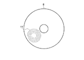
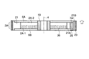
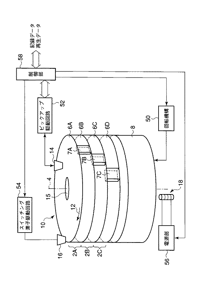
図1に示されるように記録媒体10は、その中心軸が回転中心の軸4に定められている。記録媒体10は、コイルがその内に配置されているコイル内蔵部8、この内蔵部8上に電気伝導層6A、6B、6C,6D間及び円盤状記録層2A、2B、2Cが交互に積層された積層構造を有している。即ち、この積層構造においては、電気伝導層6A、6B、6C,6D間に各記録層2A、2B、2Cが夫々配置され、また、電気伝導層6A、6B、6C,6D間には、電気抵抗体7A、7B、7Cが配置され、図2に示されるように電気伝導層6A、6B、6C,6Dが電気抵抗体7A、7B、7Cを介して電気的に直列接続されている。電気抵抗体7A、7B、7Cは、夫々対応する円盤状記録層2A、2B、2Cの外周に埋設され、回転軸4に平行な直線上に一列には配置されず、回転方向12に沿って所定の間隔を開けて配置されている。また、コイル内蔵部8内のコイルの両端は、直列接続された電気伝導層6A、6B、6C,6Dの両端に接続されている。記録媒体10及びコイル内蔵部8は、スピンドル及び回転モータを含む回転機構50によって回転可能に装置内に保持されている。この回転機構50は、制御部58によって制御され、記録媒体10及びコイル内蔵部8が所定の回転速度で回転制御される。
As shown in FIG. 1, the central axis of the
この記録媒体10上には、レーザービームを円盤状記録層2A、2B、2Cに照射するピックアップヘッド14が配置され、電気抵抗体7A、7B、7Cを導通及び非道通にさせる光源或いは微小磁石等の非接触スイッチング素子16が記録媒体10の回転時に電気抵抗体7A、7B、7Cに次々に対向されるように配置されている。スイッチング素子16は、スイッチング素子駆動回路54に接続され、制御部58によってこのスイッチング素子駆動回路54がスイッチング素子16を所定のタイミングで附勢してスイッチング素子16から光ビーム或いは磁束が発生される。また、光ピックアップ14は、光ピックアップ駆動回路52に接続され、制御部58によってこの光ピックアップ14が再生モード或いは記録モードに設定され、再生モード及び記録モードに応じて光ピックアップ14から再生用のレーザー光或いは記録用のレーザー光が発生される。また、光ピックアップ14は、光ピックアップ駆動回路52によってフォーカス制御並びにトラッキング制御されて、光ピックアップ14からのレーザー光が目的とする記録層2A、2B、2Cにフォーカスされ、記録層2A、2B、2C上のトラッキングガイドに沿ってレーザー光がガイドされて目的とする記録層2A、2B、2Cが検索される。記録層2A、2B、2Cにウォブルが設けられている場合には、制御部58において、光ピックアップ14からの信号からウォブル信号が分離され、ウォブル信号からクロック信号或いはアドレス信号が分離される。
On this
スイッチング素子16が光源であれば、スイッチング素子16と1つの電気抵抗体7A、7B、7Cとが対向されたタイミングでスイッチング素子16が附勢されてスイッチング素子16から1つの電気抵抗体7A、7B、7Cに光ビームが照射される。この光ビームによって電気抵抗体7A、7B、7Cの抵抗値が変化され、目的とする1つの記録層2A、2B、2Cに抵抗値に応じた電圧が印加される。スイッチング素子16が微小磁石にあっても、スイッチング素子16と1つの電気抵抗体7A、7B、7Cとが対向されたタイミングで磁石からの磁束が電気抵抗体7A、7B、7Cに磁束が与えられて電気抵抗体7A、7B、7Cの抵抗が同様に変化され、目的とする1つの記録層2A、2B、2Cに抵抗値に応じた電圧が印加される。ここで、光ピックアップヘッド14からのレーザー光は、目的とする1つの記録層2A、2B、2Cにフォーカスされ、その目的とする1つの記録層2A、2B、2Cがレーザー光で検索され、記録モードでは、このレーザー光で情報が目的とする1つの記録層2A、2B、2Cに書き込まれ、また、再生モードでは、このレーザー光で目的とする1つの記録層2A、2B、2Cから情報が書き出される。
If the switching
また、コイル内蔵部8の下方には、コイル内蔵部8内のコイルを励磁して誘導起電力を生じさせるための電磁石或いは永久磁石18が配置されている。
An electromagnet or
図1に示される記録媒体10のディメンションの一例について説明すれば、円盤状記録層2A、2B、2Cが夫々現行のDVDと同じ大きさであるとすると、円盤状記録層2A、2B、2C及びコイル内蔵部8を含む記録体10は、厚さが1.2mm、直径が120mmの円板で、最内周の開口部分15の直径(所謂クランプ領域の内径)は、15mmとなる。また、所謂、8cmDVDといわれる媒体と同じとすると、円盤状記録層2A、2B、2Cは、厚さが1.2mm、直径が80mmの円板で、最内周の開口部分の直径は15mmとなる。明らかなように、記録媒体10は、このようなディメンションに限らず、これ以外の大きさ・形状でも良い。尚、媒体及び装置について、特に言及していない事項については、現行DVDと同じものとする。媒体10は、回転中心軸4の周りに回転し、ピックアップヘッド14から照射されるレーザー光により後に詳述するように情報が記録層2A、2B、2Cに記録され、また、記録層2A、2B、2Cから再生される。
An example of the dimensions of the
図1においては、3層の記録層2A、2B、2Cが設けられているが、実施の形態によっては1層でも良く、100層でも良い。記録層2A、2B、2Cが積層された情報記録部分20とコイル内蔵部分8の間に反射層22が設けられても良い。また、通常は、記録層2A、2B、2Cを傷などから保護するため、記録媒体10の上面にカバー層(図示せず)が設けられることが好ましい。
In FIG. 1, three
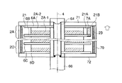
図3には、1つの記録層2Aが設けられたディスクの内部構造の一例が示されている。他の記録層を設けたディスクの内部も同様の構造が採用される。図3に示される構造では、記録層2Aとして電流を流すことで電流の向きに応じて着色と消色の状態を可逆的に変化させることのできるEC(エレクトロクロミック)材料及び電解質材料の組み合わせが用いられる。即ち、電気伝導層6A、6B間には、エレクトロクロミック材料の層2A−1及びこのエレクトロクロミック層2A−1上に電解質層2A−2が積層されて記録層2Aが構成されている。記録層2Aの内周側には、円筒状のスピンドル部19が設けられ、記録層2Aの内周側がこのスピンドル部19に接触されている。尚、このスピンドル部19には、垂直方向(回転軸に沿った方向)での電気的な接続をするための配線が設けられている。
FIG. 3 shows an example of the internal structure of a disc provided with one
また、図3に示されるように記録層2Aの外周側には、リング状の絶縁層21が電気伝導層6A、6B間に狭持されるように設けられ、この絶縁層21中に既に説明した電気抵抗体7Aが埋設されている。即ち、電気抵抗体7Aは、電気的に外部に接触されることを阻止する為に絶縁層21A、21B中に狭持されるように絶縁層21中に埋設されている。図3に示されるディスク構造では、その内部からの熱を放熱する為に絶縁層21の外周は、熱伝導体層23で覆われている。
Further, as shown in FIG. 3, a ring-shaped insulating
EC(エレクトロクロミック)材料として無機系では、酸化タングステン(WO3)と電解質中のカチオン(Hイオン、Liイオン、Naイオン、Znイオンなど)の組み合わせが代表的であるが、タングステンの替わりに他の遷移金属(チタン、バナジウム、クロム、マンガン、鉄、コバルト、ニッケル、銅、ジルコニウム、ニオブ、モリブデン、ルテニウム、ロジウム、レニウム、オスミウム、イリジウムなど)やインジウム、スズ、プラセオジム、サマリウム、ジスプロシウム、ホルミウム、エルビウム、ルテチウムなどもEC特性を示すことがわかっている。また、その他にも例として、ルテシウム−ジフタロシアニン錯体、コバルト−ピリジノポルフィラジン錯体、或いは、プルシアンブルー(Fe4(FeCN6)3)等を挙げることができる。また有機系では、希土類ジフタロシアニン、色素ペンダント型ポリマー(TTFポリマー、ピラゾリンポリマーなど)、ポリマーコンプレックス(ビオロゲンポリマーなど)、電解重合ポリマー(ポリチオフェン、ポリピロール、ポリアニリンなど)、ビオロゲン誘導体(ヘプチルビオロゲンなど)、ビピリジン錯体(コバルトビピリジンなど)、有機色素(キノン系、スチリル系、ピラゾリン系、フルオレン系、ジフェニルアミン系、ベルダジルなど)、或いは、米国H.C.Starck社のBaytron Pなどを挙げることができる。 In inorganic materials as EC (electrochromic) materials, a combination of tungsten oxide (WO 3 ) and cations (H ion, Li ion, Na ion, Zn ion, etc.) in the electrolyte is typical, but other than tungsten. Transition metals (titanium, vanadium, chromium, manganese, iron, cobalt, nickel, copper, zirconium, niobium, molybdenum, ruthenium, rhodium, rhenium, osmium, iridium, etc.), indium, tin, praseodymium, samarium, dysprosium, holmium, Erbium, lutetium, etc. are also known to exhibit EC characteristics. Other examples include lutesium-diphthalocyanine complex, cobalt-pyridinoporphyrazine complex, Prussian blue (Fe 4 (FeCN 6 ) 3 ), and the like. In organic systems, rare earth diphthalocyanines, dye pendant polymers (TTF polymers, pyrazoline polymers, etc.), polymer complexes (viologen polymers, etc.), electropolymerization polymers (polythiophene, polypyrrole, polyaniline, etc.), viologen derivatives (eg heptyl viologen, etc.) , Bipyridine complexes (such as cobalt bipyridine), organic dyes (such as quinone-based, styryl-based, pyrazoline-based, fluorene-based, diphenylamine-based, and verdadil), or Baytron P manufactured by HC Starck, USA.
電解質材料は、液体、半固体(高分子)、固体に分類できるが、安定性や応答性等の点から固体が望ましい。固体には、Hイオンを可動イオンとする誘導体(MgF2,CaF2,SiO,ZrO2,Ta2O5,Cr2O3,LiF等)、Naイオン、Liイオン、Agイオン等を可動イオンとする固体電解質(Na−β−Al2O3,Na1+xZr2SixP3−xO12,LiN,LiI,Li2WO4,RbAg4I5等)を挙げることができる。
The electrolyte material can be classified into liquid, semi-solid (polymer), and solid, but solid is desirable from the viewpoint of stability and responsiveness. The solid, derivatives of H ions and mobile ions (MgF 2, CaF 2, SiO ,
電気伝導層6A,6Bには、透明電極が用いられ、一般にはITO(インジウム−スズ酸化物)、或いは、酸化スズ(SnO2)が良く知られているが、その他にも、ZnO系、In2O3−ZnO系、In4SnO12、InGaZnO4、TiNなどを挙げることができる。
Transparent electrodes are used for the electrically
電気抵抗体7A、7B、7Cは、電圧を印加する記録層を選択するためのスイッチの役割を有し、図2に示すように、最上位及び最下位の電気伝導層6A,6Cにコイル(図示せず)から電圧が印加され、その間に直列に電気伝導層6Bと電気抵抗体7B、7Cが接続されている。通常、すべての電気抵抗体7A、7B、7Cは、その抵抗値が低い状態、或いは導通状態とした上で、選択された一つの電気抵抗体7A、7B、7Cのみを高抵抗、或いは、切断の状態とすればその間の記録層2A、2B、2Cのみを選択して電圧を印加することができ、その記録層2A、2B、2Cのみを着色或いは消色することができる。
The
電気抵抗体7A、7B、7Cの材料には、外部からの光または熱または磁気などによりその抵抗値を大きく変化させることができ、かつ、変化の回数によってその特性に変化が少ない(寿命が長い)ものが望ましく、例えば、カルコゲナイド半導体に代表される相変化材料(GaSb,InSb,InSe,SbTe,GeTe,AsSbTe,GeSbTe,InSbTe,GaSeTe,SnSbTe,InSbGe,AgInSbTe,GeSnSbTe,GeSbSeTe,TeGeSbS等)や、フォトダイオード、フォトトランジスタ、CdS,PdS,太陽電池などの光センサ、ボロメータ、熱電対、サーミスタなどの熱センサ、ホール素子、MR素子などの磁気センサ、或いはこれらとトランジスタ等電気回路との組み合わせなどを挙げることができる。さらに望ましくは、外部からの光などを遮断してもその抵抗値を保持することのできる材料であれば、記録層の着色或いは消色に必要な時間すべてにわたって外部からの光などを与え続けなくともすむため、システムの構成の面でも、消費電力の面でも、有利である。例えば、前記相変化材料はこの特性を有する材料の一つである。相変化材料は温度変化の仕方により結晶状態と非晶質状態が切り換わり、結晶状態の抵抗値を非晶質状態の抵抗値よりも低く、組成の調整によっては例えば比にして約1/103とすることが可能である。相変化材料にレーザー光などを照射して、融点を超えるまで加熱すれば冷却後に非晶質状態(高抵抗)となり、また、結晶化温度(100℃〜300℃程度)より高く融点よりも低い温度で一定時間を経過すれば結晶状態(低抵抗)となるため、レーザー光の照射を停止した後も、その抵抗値を保持することができる。
The resistance values of the materials of the
更に、図1に示されるように、電気抵抗体を円周上にずらして配置すれば、外部光源の発光のタイミングをコントロールすることで、電気抵抗体を一つだけ選択してその抵抗値を変化させることが可能である。また、電気抵抗体を回転中心軸からの距離(半径位置)を変えて配置し、外部光源の半径位置を移動させて発光することでも、同様の目的を達することができる。但し、いずれにしても、配置されたそれぞれの電気抵抗体の断面積及び厚さは、抵抗値を均一とするため、同等にすることが望ましい。また、電気抵抗体の一部分に電気的なスペーサー(導通体)を挿入することにより、電気抵抗体の厚さを調整し、電気抵抗体の抵抗値を所望のものとすることができる。 Further, as shown in FIG. 1, if the electric resistors are arranged on the circumference, the electric light source timing is controlled, so that only one electric resistor is selected and its resistance value is set. It is possible to change. Further, the same purpose can be achieved by arranging the electric resistor at a different distance (radial position) from the rotation center axis and moving the radial position of the external light source to emit light. However, in any case, it is desirable that the cross-sectional area and the thickness of each arranged electric resistor are equal to each other in order to make the resistance value uniform. In addition, by inserting an electrical spacer (conducting body) into a part of the electrical resistor, the thickness of the electrical resistor can be adjusted, and the resistance value of the electrical resistor can be set as desired.
図3に示す構造では、1対の電気伝導層6A、6Bに狭持されて電解質及びEC材料から成る記録層2Aが設けられ、外周部分は電気絶縁体21と熱伝導体23が取り巻いている。電気絶縁体23は、記録層2Aと電気抵抗体21、或いは、熱伝導体23を電気的に分離し、熱伝導体23は、電気抵抗体21の冷却速度を調整し、相変化を適切かつ安定して生じさせるためにある。熱伝導体23の更に外周にポリカーボネート樹脂などの保護材を設けても良い。また、電気抵抗体7Aの下部に光吸収膜25を用意すれば、レーザー光の吸収率を高めて電気抵抗体7Aを効率良く加熱することができる。
In the structure shown in FIG. 3, a
記録層2Aにおいて、記録材料の厚さdは、屈折率をn、光の波長をλとして、
![]()
![]()
であることが望ましい。これは、記録材料に厚さdの記録マークが形成され、この記録マークを再生する場合、再生信号の変調度が
![]()
![]()
で最大となるという条件に基づいている。またさらに、電気伝導層や記録層の厚さは、透過光の位相を考慮して、
が自然数となるように設定するのが望ましい。 It is desirable to set so that is a natural number.
尚、ここで、光の波長をλ、電気伝導層6A、6B、6Cの間隔をD、電気伝導層6A、6B、6C間にはさまれる材料の層数をN−1、材料iの屈折率をn(i)、厚さをd(i)、電気伝導層6A、6B、6Cの屈折率をn(N)、厚さをd(N)とおいており、
![]()
![]()
を満足する。このようにすることによって、透過光の位相の条件がすべての層で同一となる。 Satisfied. By doing so, the phase condition of the transmitted light is the same in all layers.
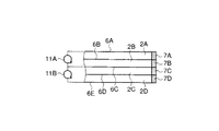
記録媒体10のコイル内蔵部分8には、図4或いは図5に示されるような配置でコイル11が内蔵される。図4に示す配置では、コイル11が回転中心軸を内包するようにスパイラル状に巻かれている。このようなコイル配置では、記録媒体10の外部の回転中心軸付近に電磁石28を設けることにより、コイル11に誘導起電力を生じさせることができる。コイル11の数は、1つでも良いし、複数のコイル11A、11Bを厚さ方向に積層して図6に示すように配線しても良い。図6に示される記録媒体10においては、4層の記録層2A〜2Dが設けられ、これらの記
録層2A〜2Dが電気伝導層6A、6B、6C、6D、6Eの間に配置されている。このような構造において、コイル11A、11Bが電気伝導層6A、6C及び電気伝導層6C、6Eに接続され、コイル11A、11Bを電源とする2つの閉回路が形成されている。即ち、電気伝導層6A、6B、6Cが電気抵抗体7A、7Bを介して直列に接続されてコイル11Aに接続され、また、電気伝導層6C、6D、6Eが電気抵抗体7C、7Dを介して直列に接続されてコイル11Bに接続されている。
The
複数のコイル11A、11Bが設けられる場合には、記録層2A〜2Dに印加される電圧にばらつきが生じないようにするため、記録層2A〜2Dの数の約数と同数にしてコイル1つあたりの記録層数が一定となるようにするとともに、コイル11A、11Bの形状をすべて同じにすることが望ましい。図5に示すように、コイル11の中心が回転中心軸4の周りに配置されてコイル11が回転中心軸を内包しないように巻かれている場合は、電磁石に代えて永久磁石を用いることもできるが、望ましくは、同一形状のコイル11を記録層2A、2B、2C、2Dの数と同一か、或いは、自然数倍だけ用意し、電気抵抗体7A、7B、7C,7Dが円周上に配置される角度間隔と同じ間隔でコイル11も配置されれば、電気抵抗体7A、7B、7C,7Dの切り換えのタイミングと誘導起電力発生のタイミングとを位相を合わせて適切に行うことができる。
In the case where a plurality of
電気抵抗体7A、7B、7C,7Dが相変化材料の場合には、相変化に必要な加熱をピックアップヘッドからのレーザー光が照射されて加熱されても良い、或いは、別途レーザー光源が設けられても良い。電気抵抗体7A、7B、7C,7Dは、1μm角〜1mm角程度の断面積にすることができるので、記録マークの大きさと同等とすることも、はるかに大きくすることもでき、別途レーザー光源を設けた場合にも、高精度な光学部品或いは制御手段を用意する必要はないし、半導体レーザーではなく、発光ダイオードなどの安価な部品を利用することもできる。電気抵抗体7A、7B、7C,7Dが前記磁気センサの場合にも、微小な電磁石をピックアップヘッドに含有して用いても良いし、別途新たに設けても良い。記録媒体10のコイル内蔵部分8の表面にはラベルの添付や印刷などを行うこともできるし、さらに、コイル内蔵部分8は透明であっても不透明であっても良い。特に、コイル内蔵部分8の外周部分が透明の場合には、前記レーザー光源の設置場所を、ピックアップヘッドに対して媒体をはさんで反対側にすることができる。
When the
記録層2A、2B、2C、2Dの着色・消色による選択は、ユーザーが行えるようにしても良いが、ユーザーが行えないようにして、貸し出し時或いは販売時に店頭においてのみ行えるようにすれば、数〜百枚程度の再生専用媒体を1枚でまかなえるため、保管スペースの削減に有効である。また、EC材料によっては、メモリ効果の期間を数日〜数年に設定することができるため、返却不要の貸し出し用媒体としての利用も可能である。これらの場合、ユーザーの使用する記録再生装置には、外部電磁石などの特殊な付加部品を必要とせず、現行DVDの記録再生装置と同等の装置で対応することができる。
The
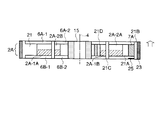
図7に示すように、ディスク構造の内周側と外周側を絶縁層21Cで分離して電気伝導層6Aを伝導層部分6A―1、6A−2に電気的に分離し、また、記録層2AをEC部2A−1A並びに電解質部2A−2Aから構成される第1の記録層部分2A−1及びEC部2A−1B並びに電解質部2A−2Bから構成される第2の記録層部分2A−2に電気的に分離しても良い。図7に示される構造では、内周側と外周側に2つに分離しているが、2以上の複数に分離しても良いことは明らかである。図7に示すように複数部分に記録層2Aを分離することによって、既に記録または再生の終了した領域の記録層部分を消色し、次に記録または再生するの記録層部分を予測して事前に着色しておくことが可能となる。このような分離構造を採用することによって、着色及び消色の待ち時間を短縮することができるようになる。但し、図7に示すように分離する為の境界は、電気的に絶縁し、電気抵抗体及びコイルなども分離した回路とすることが望ましい。
As shown in FIG. 7, the inner and outer peripheral sides of the disk structure are separated by an insulating
情報の記録または再生は、着色された記録層2A、2B、2C、2Dに対して実施される。記録は、選択されて着色された記録層2A、2B、2C、2Dに強いレーザー光を照射し加熱することで達成できる。即ち、光ピックアップ14でターゲットとされた1つの記録層2A、2B、2C、2Dにレーザーがフォーカスされ、このフォーカスされたレーザーが照射された部分は、発熱により消色され、記録マークとなる。この記録マークは、印加される電流にかかわらず透明のまま固定されるため、記録層2A、2B、2C、2Dが選択された場合のみ記録マークとして機能し、記録層2A、2B、2C、2Dが選択されずに透明である場合には、他の記録層2A、2B、2C、2Dの記録・再生には影響を及ぼさないこととなる。記録時のレーザー光の照射は、一定強度の連続照射ではなく、熱の広がりを考慮したパルス列とすることが望ましい。再生は、着色された記録層の記録マークの部分は着色されずに残るため、記録マークとその他の部分との反射率または透過率の差によって読み取ることができる。着色されていない記録層2A、2B、2C、2D及び電気伝導層6A、6B、6C、6D、6E等はすべて透明であるため、記録・再生には影響を及ぼさないこととなる。記録・再生の終了した後は、逆極性の電流を流すことにより記録層2A、2B、2C、2Dを透明に戻すことができる。
Information recording or reproduction is performed on the colored recording layers 2A, 2B, 2C, and 2D. Recording can be achieved by irradiating and heating the selected
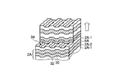
以上のような記録及び再生の方法は追記型媒体としてのものであり、フォーカス、或いは、トラッキングの制御、又は、クロック信号或いはアドレス信号の取得などのためには、図8に示すような凹凸のある所謂、ランド・グルーブ構造や一定周期で蛇行した所謂、ウォブルを有することが望ましい。即ち、記録層2A上にランド30及びグルーブ32を形成してレーザー光でのトラッキングを実現するとともにランド30及びグルーブ32の両方に情報を書き込み可能として記録密度を高めることができ、また、ランド30及びグルーブ32を蛇行させるウォブル構造34を採用しこのウォブル構造の周期を読み出したウォブル信号を抽出することによってクロック信号或いはアドレス信号をこのウォブル信号から取り出すことができる。
The recording and reproducing method as described above is a write-once medium. For the focus or tracking control or the acquisition of the clock signal or address signal, the unevenness as shown in FIG. It is desirable to have a so-called land / groove structure or a so-called wobble meandering at a constant period. That is, the
更に、アドレス情報を予め記録媒体10に埋め込んだり、再生専用媒体として情報を記録したりするため穴、所謂ピット36を、図9に示すように記録層2Aに設けることも可能である。ピット36を透明な材料で形成し、その周囲にEC材料を配置することで、記録層2Aの着色時には、ピット36を記録マークとして機能させることができる。再生専用媒体では逆に、ピット36にEC材料を配置し、その周囲に透明材料を形成することでも、同様の目的を達することができる。尚、いずれの場合でも、ピット36の高さは、EC材料の厚さと同一かそれ以上とすることが再生信号の変調度を大きくするなどの点から好ましいが、いかなる場合にも必ず達成すべき条件というわけではない。
Furthermore, holes, so-called
図1に示される光記録装置では、一例として次のような手順で情報が各記録層2A、2B、2Cに記録される。記録層2A、2B、2Cへの情報の記録及び消去は、記録層2A、2B、2Cへの着色及び消色に対応し、記録層2A、2B、2Cは、以下のようにして着色され、また、その着色が消去される。
In the optical recording apparatus shown in FIG. 1, information is recorded on each
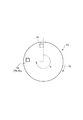
図10に示すように電気抵抗体7A、7B、7Cを附勢するスイッチング素子16の位置を基準として、着目する電気抵抗体7A、7B、7Cの回転方向に沿う回転角Φは、記録媒体10の回転とともに変化される。即ち、記録媒体10の回転に伴い、回転角Φは、図11(a)に示すように0°〜360°の間を周期的に変化される。ここで、この回転角Φに位相に合わせて電磁石18に交流電圧が印加されると、この電磁石18が励磁されて交番磁界が発生されて図4に示されるコイル11に図11(b)に示される波形の誘導電力が発生される。即ち、図11(b)に示される誘導電力は、記録媒体10が2回転されると、1周期される誘導電力が発生され、しかも、外部光源としてのスイッチング素子16が電気抵抗体7A、7B、7Cに対向される際に、誘導電力波形が0Vを通過するように設定される。
As shown in FIG. 10, with reference to the position of the switching
尚、図11(b)に示される波形においては、誘導起電力の周期が回転周期の2倍としているが、誘導起電力の周期が回転周期の自然数倍、望ましくは、偶数倍であれば、同様の目的を達することができる。 In the waveform shown in FIG. 11 (b), the period of the induced electromotive force is twice the rotation period. However, if the period of the induced electromotive force is a natural number of the rotation period, preferably an even multiple. Can reach a similar purpose.
スイッチング素子16としての光源は、図11(c)に示すように一回転毎に附勢される。但し、スイッチング素子16としての光源からの照射パワーは、1回転ごとに第1及び第2レベルH1、H2に切り換えられて電気抵抗体7A、7B、7Cの抵抗値が変化される。即ち、タイミングt1に達する直前にスイッチング素子16としての光源から第1レベルH1の光ビームが目的とする電気抵抗体7A、7B、7Cに照射されると、図11(d)に示されるように、この電気抵抗体7A、7B、7Cの状態が結晶状態から非晶質状態に変化される。従って、図11(e)に示すように目的とする電気抵抗体7A、7B、7Cの抵抗値が高抵抗となり、目的とする電気抵抗体7A、7B、7Cで互いに接続されている電気伝導層6A、6B、6C間が切断され、図11(f)に示すようにその間の記録層に2A、2B、2Cに電圧が印加される。例えば、電気抵抗体7Aの抵抗値が高抵抗となると、この電気抵抗体7Aを介して互いに接続されている電気伝導層6A、6Bが電気的に分離される。従って、電気伝導層6A、6Cに印加されているコイル内蔵部8からの誘導電圧は、低抵抗に維持された電気抵抗体7B、7C及び電気伝導層6Cを介して電気伝導層6A、6Bに印加される。従って、電気伝導層6A、6B間の記録層2Aに図11(f)に示される電圧が印加され、記録層2Aのエレクトロクロミック層2Aが着色される。記録層2Aのエレクトロクロミック層2A―1の着色は、電解質層2A−2によって維持され、周期的に記録層2Aに電圧を印加することによって十分にエレクトロクロミック層2A―1が着色され、また、その着色状態が電解質層2A−2によって維持される。
The light source as the switching
また、タイミングt2に達する直前にスイッチング素子16としての光源から第1レベルよりも低い第2レベルH2の光ビーム、例えば、レーザー光が目的とする電気抵抗体7A、7B、7Cに照射されると、図11(d)に示されるように、この電気抵抗体7A、7B、7Cの状態が非晶質状態から結晶状態に変化される。従って、図11(e)に示すように目的とする電気抵抗体7A、7B、7Cの抵抗値が低抵抗となり、目的とする電気抵抗体7A、7B、7Cで互いに接続されている電気伝導層6A、6B、6Cが互いに電気的に直列接続され、図11(f)に示すようにその間の記録層に2A、2B、2Cには、電圧が印加されなくなる。例えば、電気抵抗体7Aの抵抗値が高抵抗から低抵抗となると、この電気抵抗体7Aによって切断されていた電気伝導層6A、6Bが低抵抗の電気抵抗体7Aによって電気的に接続される。従って、電気伝導層6A、6Cに印加されているコイル内蔵部8からの誘導電圧は、低抵抗に維持された電気抵抗体7A、7B、7C及び電気伝導層6A、6B、6Cの直列接続回路に印加されるにすぎなくなる。従って、電気伝導層6A、6B間の記録層2Aには、図11(f)に示されるように電圧が印加されなくなり、期間t2−t3の間においては、着色が促進されず、期間t1―t2の間に着色された状態に、記録層2Aが電解質層2A−2によって維持される。
Further, when a light beam of a second level H2 lower than the first level, for example, a laser beam, is irradiated onto the target
同様に、タイミングt3に達する直前にスイッチング素子16から第1レベルH1の光ビームが目的とする電気抵抗体7A、7B、7Cに照射されると、図11(d)に示されるように、この電気抵抗体7A、7B、7Cの状態が結晶状態から非晶質状態に変化される。従って、図11(e)に示すように目的とする電気抵抗体7A、7B、7Cの抵抗値が高抵抗となり、目的とする電気抵抗体7A、7B、7Cで互いに接続されている電気伝導層6A、6B、6C間が再び切断され、図11(f)に示すようにその間の記録層に2A、2B、2Cに電圧が印加される。例えば、電気抵抗体7Aの抵抗値が高抵抗となると、この電気抵抗体7Aを介して互いに接続されている電気伝導層6A、6Bが再び電気的に分離される。従って、電気伝導層6A、6Cに印加されているコイル内蔵部8からの誘導電圧は、低抵抗に維持された電気抵抗体7B、7C及び電気伝導層6Cを介して電気伝導層6A、6Bに印加される。従って、電気伝導層6A、6B間の記録層2Aに図11(f)に示される電圧が印加され、記録層2Aのエレクトロクロミック層2Aが再び着色される。記録層2Aのエレクトロクロミック層2A―1の着色は、電解質層2A−2によって維持され、このように周期的に記録層2Aに電圧を印加することによって十分にエレクトロクロミック層2A―1の着色が促進され、また、その着色状態が電解質層2A−2によって維持される。
Similarly, when the target
上述した着色工程において、電気抵抗体7A、7B、7Cの抵抗値が1回転ごとに高抵抗と低抵抗を繰り返すようになるが、高抵抗と低抵抗との抵抗比を103以上とすることができる。従って、高抵抗に維持された期間のみ記録層2A、2B、2Cに電圧を印加することができ、低抵抗に維持された期間には、記録層2A、2B、2Cには、ほとんど電圧を印加させないことができる。
In the coloring step described above, the resistance values of the
記録モード時には、上述した着色工程を維持したまま、光ピックアップヘッド14から記録用のレーザー光が発生され、目的とする1つの記録層2A、2B、2Cにフォーカスされる。この記録用のレーザー光の照射でエレクトロクロミック層2A―1の着色が脱色されて透明に変化され、記録マークがエレクトロクロミック層2A―1に形成される。この透明な記録マークは、周期的に記録層2Aに電圧が印加され記録層2Aに逆電圧が印加されて記録層2Aが消色されても消去されずに、そのままに維持される。
In the recording mode, a recording laser beam is generated from the
周期的に記録層2Aに逆電圧が印加されると、この記録層2Aのエレクトロクロミック層2A―1の着色は、消失されるが、再び周期的に記録層2Aに電圧が印加されると、この記録層2Aのエレクトロクロミック層2A―1は、着色され、情報が記録用レーザー光で書き込まれた記録マークは、着色された領域中に透明なマークとして出現される。従って、再生モード時には、上述した着色工程を維持した状態で記録マークを読み取ることができる。即ち、再生モード時には、目的とする1つの記録層2A、2B、2Cに電圧を印加して着色した状態で、光ピックアップヘッド14から記録用のレーザー光よりもパワーの小さい再生用のレーザー光が発生され、目的とする1つの記録層2A、2B、2Cにフォーカスされる。この再生用のレーザー光がエレクトロクロミック層2A―1の着色領域及び透明マークに照射されると、再生用のレーザー光は、着色領域及び透明マークによって強度変調される。この強度変調された再生用のレーザー光が光ピックアップヘッド14に戻され、光ピックアップヘッド14において強度変調された再生用のレーザー光が検出されることによって再生信号に変換される。
When a reverse voltage is periodically applied to the
目的とする1つの記録層2A、2B、2Cを消色するには、スイッチング素子16としての光源からの照射のタイミングを1回転分に相当する位相だけずらして記録層2A、2B、2Cに逆電圧を印加することによって実現することができる。即ち、図12(a)に示すように記録媒体10を回転している状態において、図12(b)に示されるように図11(b)とは、位相が180度異なるタイミングでスイッチング素子16が附勢される。図12(c)に示されるスイッチング素子16が附勢されタイミングt10では、図11(b)に示される誘導電力とは、異なり誘導起電力は、逆電圧に移行される。従って、図12(d)に示すように期間t10―t12において、この電気抵抗体7A、7B、7Cが結晶状態から非晶質状態に変化されると、図12(e)に示すように目的とする電気抵抗体7A、7B、7Cの抵抗値が高抵抗に変化される。従って、図12(f)に示すように目的とする記録層2A、2B、2Cに逆電圧が印加され、記録層2A、2B、2Cが消色される。即ち、逆電圧の記録層2A、2B、2Cへの印加によって記録層2A、2B、2Cのエレクトロクロミック層2Aが消色され、記録モード時に形成された記録マークを含めて透明となる。図11を参照して説明したと同様に逆電圧を周期的に印加することによって確実に記録層2A、2B、2Cが消色される。このような逆電圧の印加を消色の終了するまで続けることで、記録層の消色が達せられる。
In order to erase one
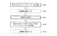
以上の動作を図13に示されるフローチャートを参照して説明すると、記録モード時には、ステップS10に示すように電気抵抗体7A、7B、7Cにスイッチング素子16としての光源からレーザー光が照射され、ステップS12に示すように目的とする記録層2A、2B、2Cが着色される。記録層2A、2B、2Cが着色された状態で、ステップS13に示すように光ピックアップ14からのレーザー光で情報が記録層2A、2B、2Cに記録され、或いは、記録層に2A、2B、2Cから情報が再生される。ステップS14に示すように記録層2A、2B、2Cを消色するには、図12に示すように図11とは異なるタイミングで電気抵抗体7A、7B、7Cにスイッチング素子16としての光源からレーザー光が照射され、目的とする記録層2A、2B、2Cに逆電圧が印加されてステップS15に示すように記録層2A、2B、2Cが消色され、形成した記録マークを含めて透明となる。
The above operation will be described with reference to the flowchart shown in FIG. 13. In the recording mode, the
図13に示すように、情報の記録または再生の前後にこのような着色及び消色の手順が繰り返えされることとなる。即ち、始めに、図11に示されるタイミングで記録層2A、2B、2Cが着色された後に、情報の記録又は情報の再生がなされ、その後、図12に示すタイミング(高パワーと低パワーが1回転分ずれたタイミング)で記録層2A、2B、2Cが消色され、すべての層が透明な状態に復旧される。 As shown in FIG. 13, such coloring and decoloring procedures are repeated before and after recording or reproducing information. That is, first, after the recording layers 2A, 2B, and 2C are colored at the timing shown in FIG. 11, information is recorded or reproduced, and then the timing shown in FIG. The recording layers 2A, 2B, and 2C are decolored at a timing shifted by the amount of rotation, and all the layers are restored to a transparent state.
尚、図5に示されたコイル11の配置と外部の永久磁石18とが組み合わされた場合には、対象となる記録層2A、2B、2Cに接続されたコイル11と永久磁石18が重なる時に回転角Φ=0°となるように設定する。このような配置においては、より好ましくは、回転角Φ=180°の位置に電気抵抗体7A、7B、7Cを追加することにより、同様の目的を達することができる。永久磁石18に代えて電磁石18を組み合わせた場合には、電磁石18に加える交流の制御により、電気抵抗体7A、7B、7Cの追加を省略することができる。
When the arrangement of the
図14及び図15を参照して、この発明の他の実施形態に係る光記録装置を説明する。図14及び図15に示される記録媒体10においては、記録層2A、2B、2Cなどの構成は前述の構成と同様であるので、同一部分には同一の符号を付してその詳細な説明を省略する。
An optical recording apparatus according to another embodiment of the present invention will be described with reference to FIGS. In the
図14及び図15に示される記録媒体10は、いずれも記録媒体10がコイル11を内蔵せず、電力供給のために記録媒体10の内表面側に1対の電極62、64が設けられている。図14に示される構造では、媒体電極62は、回転軸のクランプ装置66で挟み込まれるスピンドル部19内を延出され、最上位の電気伝導層6Aに接続され、また、媒体電極64は、最下位の電気伝導層6Dに接続されている。両媒体電極62、64は、記録媒体10の下面又は最内周開口部の内壁にまで延出されて端子として露出されている。また、図15に示される構造では、媒体電極62、64は、夫々回転軸のクランプ装置66で挟み込まれる中空状のスピンドル部19の内表面を延出され、最上位の電気伝導層6A及び最下位の電気伝導層6Dに接続されている。両媒体電極62、64は、同様に記録媒体10の下面又は最内周開口部の内壁にまで延出されて端子として露出されている。
The
図14及び図15の構造においては、媒体電極62、64の端子は、回転軸のクランプ装置66に設けられた板バネなどの装置電極と接続されている。媒体電極62、64と装置電極66のずれを防止するため、記録媒体10にノッチ等の位置あわせ手段を設けることが望ましい。
14 and 15, the terminals of the
尚、図14及び図15の構造においては、記録媒体10は、円筒筒状のハウジング70内に収納され、このハウジング70の光源側開口部がカバー層71で覆われ、光源とは反対側の開口部が反射層をその内面に有するカバー層72で覆われている。カバー層72に反射層を設けることによって最下位の記録層2Dでの書き込み時におけるレーザー光の減衰を補うことができ、確実に記録層2Dでの書き込みを実現することができる。
14 and 15, the
クランプ装置66の回転軸への電力供給は、図16に示すようにベアリング、或いは、ブラシ80、又は、コイル82等の回転用接続端子を介して実現される。ベアリング、或いは、ブラシ80に対しては、クランプ装置66の回転軸にベアリング、或いは、ブラシ80が接触される電力供給用電極81が設けられ、電力供給用電極81は、媒体電極62、64の端子に接触されるべき装置側端子86、87に接続される。また、回転用接続端子としてコイル82が採用される場合には、更に、回転軸外に電磁石或いは永久磁石84が用意され、電磁石或いは永久磁石84によってコイル82に誘導起電力が発生される。
The power supply to the rotating shaft of the
電力供給用電極81或いはコイル82に供給された電力は、前述したタイミングが達せられるように、周波数変換回路88によって周波数と位相とが調整されても良く、図5に示されたコイル11を使用する場合と同様にコイル82と電磁石または永久磁石84の組み合わせが採用されても良い。
The frequency and phase of the power supplied to the
2A、2B、2C...記録層、4...回転中心の軸、6A、6B、6C,6D...電気伝導層、7A、7B、7C...電気抵抗体、8...コイル内蔵部、10...記録媒体、14...光ピックアップ、16...スイッチング素子、19...スピンドル部、21...電気抵抗体、21A、21B...絶縁層、23...熱伝導層、36...ピット、50...回転機構、54...スイッチング素子駆動回路、58...制御部、88...周波数変換回路 2A, 2B, 2C. . . 3. recording layer; . . Axis of rotation, 6A, 6B, 6C, 6D. . . Electrically conductive layers, 7A, 7B, 7C. . . Electrical resistor, 8. . . 9. Coil built-in part . . Recording medium, 14. . . Optical pickup, 16. . . Switching element, 19. . . Spindle part, 21. . . Electrical resistor, 21A, 21B. . . Insulating layer, 23. . . Heat conductive layer, 36. . . Pits, 50. . . Rotation mechanism, 54. . . Switching element drive circuit, 58. . . Control unit, 88. . . Frequency conversion circuit
Claims (21)
互いに対向して配置され、前記電気抵抗体が低抵抗であるときに電気的に接続され、前記電気抵抗体が高抵抗にあるときに実質的に互いに絶縁される第1及び第2の電気伝導層と、
この第1及び第2の電気伝導層間に設けられ、前記第1及び第2の電気伝導層が絶縁された状態で、前記第1及び第2の電気伝導層間に印加される電圧に応じて透明状態及び着色状態の一方に遷移し、光ビームで記録マークが着色状態の領域に形成される記録層と、
を具備することを特徴とする情報記録媒体。 An electrical resistor that can be switched to one of high resistance and low resistance in a non-contact manner from the outside;
First and second electrical conductions disposed opposite each other and electrically connected when the electrical resistor is low resistance and substantially insulated from each other when the electrical resistor is high resistance Layers,
Transparent between the first and second electrically conductive layers, with the first and second electrically conductive layers being insulated and in accordance with the voltage applied between the first and second electrically conductive layers. A recording layer in which a recording mark is formed in a colored state region with a light beam, transitioning to one of a state and a colored state;
An information recording medium comprising:
互いに対向して配置され、前記第1の電気抵抗体が低抵抗であるときに前記第1の抵抗体に電気的に接続され、前記第1の電気抵抗体が高抵抗にあるときに実質的に前記第1の抵抗体に対して絶縁される第1及び第2の電気伝導層と、
前記第2の電気伝導層に対向して配置され、前記第2の電気抵抗体が低抵抗であるときに前記第2の電気伝導層に電気的に接続され、前記第2の電気抵抗体が高抵抗にあるときに実質的に前記第2の電気伝導層に対して絶縁される第3の電気伝導層と、
この第1及び第2の電気伝導層間に設けられ、前記第1及び第2の電気伝導層が絶縁された状態で、前記第1及び第2の電気伝導層間に印加される電圧に応じて透明状態及び着色状態の一方に遷移し、光ビームで記録マークが着色状態の領域に形成される第1の記録層と、
前記第2及び第3の電気伝導層間に設けられ、前記第2及び第3の電気伝導層が絶縁された状態で、前記第2及び第3の電気伝導層間に印加される電圧に応じて透明状態及び着色状態の一方に遷移し、光ビームで記録マークが着色状態の領域に形成される第2の記録層と、
を具備することを特徴とする情報記録媒体。 A first and a second electric resistor that can be independently switched to one of high resistance and low resistance in a non-contact manner from the outside;
Arranged opposite each other, electrically connected to the first resistor when the first electrical resistor is low resistance, and substantially when the first electrical resistor is high resistance And first and second electrically conductive layers insulated from the first resistor,
The second electric conductive layer is disposed opposite to the second electric conductive layer, and is electrically connected to the second electric conductive layer when the second electric resistive element has a low resistance. A third electrically conductive layer that is substantially insulated from said second electrically conductive layer when at a high resistance;
Transparent between the first and second electrically conductive layers, with the first and second electrically conductive layers being insulated and in accordance with the voltage applied between the first and second electrically conductive layers. A first recording layer that transitions to one of a colored state and a recording mark formed in a colored state region with a light beam;
Transparent between the second and third electrically conductive layers, with the second and third electrically conductive layers insulated, and transparent according to the voltage applied between the second and third electrically conductive layers A second recording layer that transitions to one of a state and a colored state, and a recording mark is formed in a colored state region with a light beam;
An information recording medium comprising:
前記電気抵抗層を高抵抗として前記第1及び第2の電気伝導層を絶縁された状態として、前記第1及び第2の電気伝導層間に電圧を印加して前記記録層を前記着色状態に遷移させる電圧供給部と、
光ビームを前記記録層に向けて前記着色状態の領域に記録マークを形成するピックアップヘッドと、
を具備することを特徴とする情報記録再生装置。 An electrical resistor that can be switched to one of high resistance and low resistance in a non-contact manner from the outside, is disposed opposite to each other, and is electrically connected when the electrical resistor is low resistance, and the electrical resistor is high resistance And a recording layer that is provided between the first and second electrically conductive layers and transitions to one of a transparent state and a colored state. An information recording medium to
The recording layer is changed to the colored state by applying a voltage between the first and second electric conductive layers, with the electric resistance layer being a high resistance and the first and second electric conductive layers being insulated. A voltage supply unit
A pickup head for forming a recording mark in the colored region with a light beam directed toward the recording layer;
An information recording / reproducing apparatus comprising:
この相対的移動に同期して前記スイッチング素子を附勢する附勢回路と、
を更に具備することを特徴とする請求項16の情報記録再生装置。 A moving mechanism for relatively moving the information recording medium and the switching element;
An energizing circuit energizing the switching element in synchronization with the relative movement;
The information recording / reproducing apparatus according to claim 16, further comprising:
前記電圧供給部は、前記コイルに磁束を供給して誘導起電力を生じさせる電磁石を更に具備することを特徴とする請求項16の情報記録再生装置。 The information recording medium includes a coil electrically connected to the first and second electrically conductive layers,
17. The information recording / reproducing apparatus according to claim 16, wherein the voltage supply unit further comprises an electromagnet that generates an induced electromotive force by supplying a magnetic flux to the coil.
前記電圧供給部は、前記コイルに磁束を供給して誘導起電力を生じさせる永久磁石を更に具備することを特徴とする請求項16の情報記録再生装置。 The information recording medium includes a coil electrically connected to the first and second electrically conductive layers,
The information recording / reproducing apparatus according to claim 16, wherein the voltage supply unit further includes a permanent magnet that supplies a magnetic flux to the coil to generate an induced electromotive force.
Priority Applications (1)
| Application Number | Priority Date | Filing Date | Title |
|---|---|---|---|
| JP2004103849A JP4110111B2 (en) | 2004-03-31 | 2004-03-31 | Optical recording medium and optical recording apparatus |
Applications Claiming Priority (1)
| Application Number | Priority Date | Filing Date | Title |
|---|---|---|---|
| JP2004103849A JP4110111B2 (en) | 2004-03-31 | 2004-03-31 | Optical recording medium and optical recording apparatus |
Publications (2)
| Publication Number | Publication Date |
|---|---|
| JP2005293661A true JP2005293661A (en) | 2005-10-20 |
| JP4110111B2 JP4110111B2 (en) | 2008-07-02 |
Family
ID=35326440
Family Applications (1)
| Application Number | Title | Priority Date | Filing Date |
|---|---|---|---|
| JP2004103849A Expired - Fee Related JP4110111B2 (en) | 2004-03-31 | 2004-03-31 | Optical recording medium and optical recording apparatus |
Country Status (1)
| Country | Link |
|---|---|
| JP (1) | JP4110111B2 (en) |
Cited By (1)
| Publication number | Priority date | Publication date | Assignee | Title |
|---|---|---|---|---|
| WO2007102298A1 (en) * | 2006-03-09 | 2007-09-13 | Pioneer Corporation | Rotary drive apparatus and electron beam irradiation apparatus |
-
2004
- 2004-03-31 JP JP2004103849A patent/JP4110111B2/en not_active Expired - Fee Related
Cited By (1)
| Publication number | Priority date | Publication date | Assignee | Title |
|---|---|---|---|---|
| WO2007102298A1 (en) * | 2006-03-09 | 2007-09-13 | Pioneer Corporation | Rotary drive apparatus and electron beam irradiation apparatus |
Also Published As
| Publication number | Publication date |
|---|---|
| JP4110111B2 (en) | 2008-07-02 |
Similar Documents
| Publication | Publication Date | Title |
|---|---|---|
| JP4120268B2 (en) | Information recording medium and information recording method | |
| US7263053B2 (en) | Information recording method and information recording apparatus | |
| TWI289833B (en) | Information recording device, information recording medium and information recording method | |
| JP4110111B2 (en) | Optical recording medium and optical recording apparatus | |
| JP2006031889A (en) | Information recording medium, information recording apparatus, and information recording method | |
| US20050052983A1 (en) | Method and apparatus for electro-optical disk memory | |
| JP2005175202A (en) | Recording element | |
| JP2006268888A (en) | Information recording apparatus, information recording medium and information recording method | |
| JP4676372B2 (en) | Multilayer optical recording medium, information recording method, and information reproducing method | |
| JP2018533810A (en) | Medium, system and method for optical data storage | |
| JP2006520059A (en) | Multi-layer hoisting information carrier | |
| JP4165511B2 (en) | Information recording device | |
| KR20040056274A (en) | An information storage medium and an optical device using the medium | |
| US20070001110A1 (en) | Optical scanning device | |
| JP4100398B2 (en) | Information recording medium | |
| WO2006043356A1 (en) | Optical recording medium recording/reproducing method, optical recording medium, and recording/reproducing device for the same | |
| Orlic | Optical information storage and recovery | |
| JP4330129B2 (en) | Optical recording medium, method for manufacturing the optical recording medium, optical recording / reproducing method, and optical information recording / reproducing apparatus | |
| CN1805020B (en) | Equipment for recording angular multiplexing pits | |
| US20070058518A1 (en) | Imformation recording medium and method for manufacturing the same | |
| JP2005203046A (en) | Information recording medium, information recording method, and recording apparatus | |
| KR100590523B1 (en) | Information recording media, apparatuses using the same, and information recording / playback methods | |
| TW200522048A (en) | Multi-layer information carrier with switching circuit | |
| RU2003108835A (en) | RECORDING AND PLAYBACK DEVICE FOR RECORDING AND PLAYING INFORMATION ON AND FROM MAGNETO-OPTICAL RECORDING MEDIA | |
| JP2008165898A (en) | Multilayer optical recording medium, information recording method and information reproducing method |
Legal Events
| Date | Code | Title | Description |
|---|---|---|---|
| A977 | Report on retrieval |
Free format text: JAPANESE INTERMEDIATE CODE: A971007 Effective date: 20060725 |
|
| A131 | Notification of reasons for refusal |
Free format text: JAPANESE INTERMEDIATE CODE: A131 Effective date: 20060808 |
|
| A521 | Request for written amendment filed |
Free format text: JAPANESE INTERMEDIATE CODE: A523 Effective date: 20061010 |
|
| A131 | Notification of reasons for refusal |
Free format text: JAPANESE INTERMEDIATE CODE: A131 Effective date: 20071218 |
|
| A521 | Request for written amendment filed |
Free format text: JAPANESE INTERMEDIATE CODE: A523 Effective date: 20080201 |
|
| TRDD | Decision of grant or rejection written | ||
| A01 | Written decision to grant a patent or to grant a registration (utility model) |
Free format text: JAPANESE INTERMEDIATE CODE: A01 Effective date: 20080401 |
|
| A61 | First payment of annual fees (during grant procedure) |
Free format text: JAPANESE INTERMEDIATE CODE: A61 Effective date: 20080407 |
|
| FPAY | Renewal fee payment (event date is renewal date of database) |
Free format text: PAYMENT UNTIL: 20110411 Year of fee payment: 3 |
|
| FPAY | Renewal fee payment (event date is renewal date of database) |
Free format text: PAYMENT UNTIL: 20110411 Year of fee payment: 3 |
|
| LAPS | Cancellation because of no payment of annual fees |