JP4120268B2 - Information recording medium and information recording method - Google Patents
Information recording medium and information recording method Download PDFInfo
- Publication number
- JP4120268B2 JP4120268B2 JP2002151713A JP2002151713A JP4120268B2 JP 4120268 B2 JP4120268 B2 JP 4120268B2 JP 2002151713 A JP2002151713 A JP 2002151713A JP 2002151713 A JP2002151713 A JP 2002151713A JP 4120268 B2 JP4120268 B2 JP 4120268B2
- Authority
- JP
- Japan
- Prior art keywords
- recording
- layer
- voltage
- electrode
- recording medium
- Prior art date
- Legal status (The legal status is an assumption and is not a legal conclusion. Google has not performed a legal analysis and makes no representation as to the accuracy of the status listed.)
- Expired - Fee Related
Links
Images


Classifications
-
- G—PHYSICS
- G11—INFORMATION STORAGE
- G11B—INFORMATION STORAGE BASED ON RELATIVE MOVEMENT BETWEEN RECORD CARRIER AND TRANSDUCER
- G11B13/00—Recording simultaneously or selectively by methods covered by different main groups among G11B3/00, G11B5/00, G11B7/00 and G11B9/00; Record carriers therefor not otherwise provided for; Reproducing therefrom not otherwise provided for
- G11B13/04—Recording simultaneously or selectively by methods covered by different main groups among G11B3/00, G11B5/00, G11B7/00 and G11B9/00; Record carriers therefor not otherwise provided for; Reproducing therefrom not otherwise provided for magnetically or by magnetisation and optically or by radiation, for changing or sensing optical properties
- G11B13/045—Recording simultaneously or selectively by methods covered by different main groups among G11B3/00, G11B5/00, G11B7/00 and G11B9/00; Record carriers therefor not otherwise provided for; Reproducing therefrom not otherwise provided for magnetically or by magnetisation and optically or by radiation, for changing or sensing optical properties combined recording by magnetic and optic means
-
- G—PHYSICS
- G11—INFORMATION STORAGE
- G11B—INFORMATION STORAGE BASED ON RELATIVE MOVEMENT BETWEEN RECORD CARRIER AND TRANSDUCER
- G11B11/00—Recording on or reproducing from the same record carrier wherein for these two operations the methods are covered by different main groups of groups G11B3/00 - G11B7/00 or by different subgroups of group G11B9/00; Record carriers therefor
- G11B11/002—Recording on or reproducing from the same record carrier wherein for these two operations the methods are covered by different main groups of groups G11B3/00 - G11B7/00 or by different subgroups of group G11B9/00; Record carriers therefor using recording by perturbation of the physical or electrical structure
-
- G—PHYSICS
- G11—INFORMATION STORAGE
- G11B—INFORMATION STORAGE BASED ON RELATIVE MOVEMENT BETWEEN RECORD CARRIER AND TRANSDUCER
- G11B7/00—Recording or reproducing by optical means, e.g. recording using a thermal beam of optical radiation by modifying optical properties or the physical structure, reproducing using an optical beam at lower power by sensing optical properties; Record carriers therefor
- G11B7/004—Recording, reproducing or erasing methods; Read, write or erase circuits therefor
- G11B7/0045—Recording
- G11B7/00455—Recording involving reflectivity, absorption or colour changes
-
- G—PHYSICS
- G11—INFORMATION STORAGE
- G11B—INFORMATION STORAGE BASED ON RELATIVE MOVEMENT BETWEEN RECORD CARRIER AND TRANSDUCER
- G11B7/00—Recording or reproducing by optical means, e.g. recording using a thermal beam of optical radiation by modifying optical properties or the physical structure, reproducing using an optical beam at lower power by sensing optical properties; Record carriers therefor
- G11B7/24—Record carriers characterised by shape, structure or physical properties, or by the selection of the material
- G11B7/2403—Layers; Shape, structure or physical properties thereof
- G11B7/24033—Electrode layers
-
- G—PHYSICS
- G11—INFORMATION STORAGE
- G11B—INFORMATION STORAGE BASED ON RELATIVE MOVEMENT BETWEEN RECORD CARRIER AND TRANSDUCER
- G11B7/00—Recording or reproducing by optical means, e.g. recording using a thermal beam of optical radiation by modifying optical properties or the physical structure, reproducing using an optical beam at lower power by sensing optical properties; Record carriers therefor
- G11B7/24—Record carriers characterised by shape, structure or physical properties, or by the selection of the material
- G11B7/241—Record carriers characterised by shape, structure or physical properties, or by the selection of the material characterised by the selection of the material
- G11B7/252—Record carriers characterised by shape, structure or physical properties, or by the selection of the material characterised by the selection of the material of layers other than recording layers
- G11B7/257—Record carriers characterised by shape, structure or physical properties, or by the selection of the material characterised by the selection of the material of layers other than recording layers of layers having properties involved in recording or reproduction, e.g. optical interference layers or sensitising layers or dielectric layers, which are protecting the recording layers
- G11B7/2578—Record carriers characterised by shape, structure or physical properties, or by the selection of the material characterised by the selection of the material of layers other than recording layers of layers having properties involved in recording or reproduction, e.g. optical interference layers or sensitising layers or dielectric layers, which are protecting the recording layers consisting essentially of inorganic materials
-
- G—PHYSICS
- G11—INFORMATION STORAGE
- G11B—INFORMATION STORAGE BASED ON RELATIVE MOVEMENT BETWEEN RECORD CARRIER AND TRANSDUCER
- G11B7/00—Recording or reproducing by optical means, e.g. recording using a thermal beam of optical radiation by modifying optical properties or the physical structure, reproducing using an optical beam at lower power by sensing optical properties; Record carriers therefor
- G11B2007/0003—Recording, reproducing or erasing systems characterised by the structure or type of the carrier
- G11B2007/0009—Recording, reproducing or erasing systems characterised by the structure or type of the carrier for carriers having data stored in three dimensions, e.g. volume storage
- G11B2007/0013—Recording, reproducing or erasing systems characterised by the structure or type of the carrier for carriers having data stored in three dimensions, e.g. volume storage for carriers having multiple discrete layers
-
- G—PHYSICS
- G11—INFORMATION STORAGE
- G11B—INFORMATION STORAGE BASED ON RELATIVE MOVEMENT BETWEEN RECORD CARRIER AND TRANSDUCER
- G11B7/00—Recording or reproducing by optical means, e.g. recording using a thermal beam of optical radiation by modifying optical properties or the physical structure, reproducing using an optical beam at lower power by sensing optical properties; Record carriers therefor
- G11B7/24—Record carriers characterised by shape, structure or physical properties, or by the selection of the material
- G11B7/241—Record carriers characterised by shape, structure or physical properties, or by the selection of the material characterised by the selection of the material
- G11B7/242—Record carriers characterised by shape, structure or physical properties, or by the selection of the material characterised by the selection of the material of recording layers
- G11B7/243—Record carriers characterised by shape, structure or physical properties, or by the selection of the material characterised by the selection of the material of recording layers comprising inorganic materials only, e.g. ablative layers
- G11B2007/24302—Metals or metalloids
- G11B2007/24312—Metals or metalloids group 14 elements (e.g. Si, Ge, Sn)
-
- G—PHYSICS
- G11—INFORMATION STORAGE
- G11B—INFORMATION STORAGE BASED ON RELATIVE MOVEMENT BETWEEN RECORD CARRIER AND TRANSDUCER
- G11B7/00—Recording or reproducing by optical means, e.g. recording using a thermal beam of optical radiation by modifying optical properties or the physical structure, reproducing using an optical beam at lower power by sensing optical properties; Record carriers therefor
- G11B7/24—Record carriers characterised by shape, structure or physical properties, or by the selection of the material
- G11B7/241—Record carriers characterised by shape, structure or physical properties, or by the selection of the material characterised by the selection of the material
- G11B7/242—Record carriers characterised by shape, structure or physical properties, or by the selection of the material characterised by the selection of the material of recording layers
- G11B7/243—Record carriers characterised by shape, structure or physical properties, or by the selection of the material characterised by the selection of the material of recording layers comprising inorganic materials only, e.g. ablative layers
- G11B2007/24302—Metals or metalloids
- G11B2007/24314—Metals or metalloids group 15 elements (e.g. Sb, Bi)
-
- G—PHYSICS
- G11—INFORMATION STORAGE
- G11B—INFORMATION STORAGE BASED ON RELATIVE MOVEMENT BETWEEN RECORD CARRIER AND TRANSDUCER
- G11B7/00—Recording or reproducing by optical means, e.g. recording using a thermal beam of optical radiation by modifying optical properties or the physical structure, reproducing using an optical beam at lower power by sensing optical properties; Record carriers therefor
- G11B7/24—Record carriers characterised by shape, structure or physical properties, or by the selection of the material
- G11B7/241—Record carriers characterised by shape, structure or physical properties, or by the selection of the material characterised by the selection of the material
- G11B7/242—Record carriers characterised by shape, structure or physical properties, or by the selection of the material characterised by the selection of the material of recording layers
- G11B7/243—Record carriers characterised by shape, structure or physical properties, or by the selection of the material characterised by the selection of the material of recording layers comprising inorganic materials only, e.g. ablative layers
- G11B2007/24302—Metals or metalloids
- G11B2007/24316—Metals or metalloids group 16 elements (i.e. chalcogenides, Se, Te)
-
- G—PHYSICS
- G11—INFORMATION STORAGE
- G11B—INFORMATION STORAGE BASED ON RELATIVE MOVEMENT BETWEEN RECORD CARRIER AND TRANSDUCER
- G11B7/00—Recording or reproducing by optical means, e.g. recording using a thermal beam of optical radiation by modifying optical properties or the physical structure, reproducing using an optical beam at lower power by sensing optical properties; Record carriers therefor
- G11B7/004—Recording, reproducing or erasing methods; Read, write or erase circuits therefor
- G11B7/0045—Recording
- G11B7/00454—Recording involving phase-change effects
-
- G—PHYSICS
- G11—INFORMATION STORAGE
- G11B—INFORMATION STORAGE BASED ON RELATIVE MOVEMENT BETWEEN RECORD CARRIER AND TRANSDUCER
- G11B7/00—Recording or reproducing by optical means, e.g. recording using a thermal beam of optical radiation by modifying optical properties or the physical structure, reproducing using an optical beam at lower power by sensing optical properties; Record carriers therefor
- G11B7/004—Recording, reproducing or erasing methods; Read, write or erase circuits therefor
- G11B7/006—Overwriting
-
- G—PHYSICS
- G11—INFORMATION STORAGE
- G11B—INFORMATION STORAGE BASED ON RELATIVE MOVEMENT BETWEEN RECORD CARRIER AND TRANSDUCER
- G11B7/00—Recording or reproducing by optical means, e.g. recording using a thermal beam of optical radiation by modifying optical properties or the physical structure, reproducing using an optical beam at lower power by sensing optical properties; Record carriers therefor
- G11B7/24—Record carriers characterised by shape, structure or physical properties, or by the selection of the material
- G11B7/241—Record carriers characterised by shape, structure or physical properties, or by the selection of the material characterised by the selection of the material
- G11B7/252—Record carriers characterised by shape, structure or physical properties, or by the selection of the material characterised by the selection of the material of layers other than recording layers
- G11B7/258—Record carriers characterised by shape, structure or physical properties, or by the selection of the material characterised by the selection of the material of layers other than recording layers of reflective layers
Description
【0001】
【発明の属する技術分野】
本発明は、光を用いて情報を記録、再生する情報記録媒体、情報記録方法、及び情報記録装置に関する。
【0002】
【従来の技術】
光ディスクでは、記録媒体(ディスク)を記録再生装置から外せることと、記録媒体が安価であることが大きな特長になっている。従って光ディスク装置では、この特徴を失わずに高速・高密度化するのが望ましい。
【0003】
記録膜に光を照射して情報を記録する原理は種々知られているが、そのうちで膜材料の相変化(相転移、相変態とも呼ばれる)など、熱による原子配列変化を利用するものは多数回書換え可能な情報記録媒体が得られるという長所を持つ。例えば、特開2001―344807号に記載されている通り、これら相変化光ディスクの場合の基本構成は基板上に保護層、GeSbTe系等の記録膜、保護層、反射層という構成からなる。
【0004】
一方、記録膜に電界を印加した状態でレーザ光を照射することによって、相変化記録膜に情報の記録を行う、電界効果型光ディスクが知られている。これは、上下の電極間にGeSbTe系などの相変化記録層をサンドイッチにした素子構造で使用される。この電界効果型光ディスクは、例えば、特開昭63−122032号に記載されている。記録膜に電界がかかることにより、レーザー光照射だけよりも相変化(結晶化)が促進されることを狙ったものである。構成を図1に示す。光9はレンズ8で集光され、光入射側から、基板7、透明電極1、UV樹脂案内溝層2、記録膜3,断熱電極4,Al電極5,保護層6の層を有し、透明電極とAl電極に電圧が印加される。この表面に案内溝を有するUV樹脂層2は、比抵抗が106Ω・cmの絶縁物であって、電界バッファ層としての機能と、案内溝を形成するための機能とを有している。
【0005】
また、本願発明者らの論文:M.Terao, H.Yamamoto and E. Maruyama : Highly Sensitive Amorphous Optical Memory: supplement to the J. of the Japan Society of Applied Physics Vol.42, pp233-238 には、光伝導体と相変化記録膜を透明電極で挟み、この透明電極で電圧を印加しながら光を照射すると、光照射だけの場合に比べて2桁近く弱いレーザー光で記録できる実験結果が報告されている。 一方、有機材料を記録層とした光ディスクで実用化しているものには、CD−RやDVD−Rが有る。これらは、記録光源の波長に吸収を有する色素を含む記録層と、それに接する基板表面をレーザー照射で変質させて記録を行う。
【0006】
【発明が解決しようとする課題】
高速化が重要であるが、光ディスクはディスクを装置に着脱できるのと、記録媒体にプラスチック基板を用いて低価格であるのが特徴であるから、ディスクの外周部の上下振れや偏心は避け難い。上下振れや偏心は回転数を上げると高周波となるので、オートフォーカスやトラッキングの追従が困難となる。従って装置の機械的振動追従の限界を越えて高速化するには、特に影響が出やすい記録時に、記録媒体がトラッキングズレなどに寛容である必要がある。
【0007】
本願発明者らの上記supplement to the J. of the Japan Society of Applied Physics Vol.42の論文の技術、及び、特開昭63−122032号に記載の電界効果型媒体では、ランド部もグルーブ部もほぼ同じ電圧、同じ光吸収となるため、ランド、グルーブのどちらか一方だけ記録しやすい状況にはない。従ってトラッキング外れに対する許容度は大きくなく、十分な高速記録を行えない。一方、CD−RやDVD−Rもランド部とグルーブ部分の光吸収に実質的な差は無く、電流による記録の補助も困難である。
【0008】
本発明の目的はこれらの問題点を解決し、安定な大容量超高速記録を達成することにある。
【0009】
【課題を解決するための手段】
上記の問題点を解決するための本発明の構成を以下に述べる。
【0010】
ただし、本発明では、基板の凹部で溝となっている部分をグルーブと呼ぶ。グルーブとグルーブの間をランドと呼ぶ。光が基板を通して膜に入射する場合は、入射側から見てグルーブは凸に見える。このため、光を基板と反対の側から入射させる方式でも、同様に入射側から見て凸となっている側がグルーブと呼ばれる場合も有る。この部分は、基板だけに注目したときは凸部であってグルーブとグルーブの間のランド部分であるから、この呼び方は本発明の定義とは逆ということになる。ランドとグルーブの一方だけに記録する、いわゆるイングルーブ記録の場合、光入射が基板側からの場合も基板と反対側からの場合も光入射側から見て凸部に記録した方が記録特性が良い場合が多いが、大きな差ではないので光入射側から見て凹部に記録しても良い。
本発明の構成は、具体的には、以下のとおりである。
(1)基板上に、第1の電極、エレクトロクロミック材料、第2の電極が設けられ、第1の領域ではエレクトロクロミック材料層が発色し、第2の領域ではエレクトロクロミック材料層が発色しない構成とする。ここで、第1の領域はランド部、第2の領域はグルーブ部に相当し、第1または第2の領域だけに光吸収することから、記録されやすい範囲が特定される。従って、光スポットの位置や集光度が多少変わっても同じように記録され、AF,トラッキングのズレに寛容で、高速記録が可能となる。さらに、高密度記録を達成できる。
【0011】
ここで、この構成を図2に示す。ここでは、理解しやすくするため、光は図面の上側から入射するように図示した。媒体は、光入射側から、基板17,保護層11,第1の電極(透明電極)12、エレクトロクロミック材料層13,第2の電極14、UV硬化樹脂層14、保護基板16から構成され、18はグルーブ部、19はランド部に相当する。エレクトロクロミック材料13は、グルーブ部分で膜厚が大きく、ランド部分で膜厚が小さくなっている。記録層(エレクトロクロミック材料層)と第1の電極または第2の電極との間に他の層、例えば薄い絶縁物層や界面層と呼ばれる層が介在してもよい。厚さは20nm以下が望ましい。
【0012】
あるいは、基板上に、第1の電極と、第1の電極上に貫通する開口部を有する絶縁膜と、その開口部から絶縁膜上にわたって形成された、情報を記録する記録膜と、その記録膜上に形成された、第2の電極とを有する構成とする。図3では、絶縁層25の表面を平坦化しているため、ランドではほとんど膜が形成されておらず、結果として、実質的に電流が流れる開口部となっている。ここで、ランド部とグルーブ部の一方は、絶縁膜の開口部となっており、ランド部とグルーブ部の他方は、絶縁膜が形成された領域となるようにする。そうすると、グルーブ部(またはランド部)だけが絶縁層の開口部となっていて上下の電極が近接し電流が流れるが、一方で、ランド部(またはグルーブ部)には絶縁層が設けられていてほとんど電流が流れない。従って、電流の流れる範囲が限られ記録されやすい範囲が限定される。
【0013】
従って、光スポットの位置や集光度が多少変わっても同じように記録され、AF,トラッキングのズレに寛容で、高速記録が可能となる。さらに、高密度記録を達成できる。
【0014】
エレクトロクロミック記録層と第1または第2の電極との間に相変化記録層(たとえばGe2Sb2Te5の層)を設けても良い。光入射側と反対側に設けるのが光学的により好ましい。この場合、エレクトロクロミック層は記録しきい値が高いもの、相変化記録層にはSb4Te3S2など硫黄を含む低融点のものを選んで相変化記録層にのみ記録が起こるようにするか、エレクトロクロミック層を除去してもよい。
【0015】
(2)また、図3の通り、第1または第2の電極22と記録膜24との間に、光導電体層23を設けた構成としても良い。光導電体層は記録膜より光入射側の電極寄りに設けるのが良い。この場合には、光照射によって光導電体層23で発生したフォトキャリアが移動することによって光導電体層の抵抗が下がり、記録層24にかかる電圧と電流が急激に増大し、光照射部分の記録層の温度が上昇する。これにより記録層を記録状態にする。キャリアをアバランシェ増倍効果により増加させてもよい。このように、光導電体膜を設けると高密度電流を記録膜に流すことができるため、光照射のエネルギーを小さくできる。エレクトロクロミック材料層が光導電体層を兼ねても良い。
【0016】
但し、記録層が光導電体層を兼ねている、あるいは、記録層が温度上昇により電気抵抗が低下するタイプのものであってもよい。Ge−Sb−Teなどのカルコゲナイド材料やポリチオフェンなどの有機導電性材料が温度上昇により電気抵抗が低下するタイプに該当する。なお、図中、21は保護層、22は透明電極、25は絶縁体層、26は第2の電極。27は張り合わせ基板である。UV接着剤層はここでは省略している。
【0017】
(3)円形の情報記録媒体を用い、第1、第2の電極に電流を供給するために、情報記録媒体の半径方向に細長く、第1の電極または第2の電極に電流を供給するための第3の電極を設けると良い。このように第3の電極を設けると、外周まで同じ電圧を印加できる。
【0018】
(4)第1の電極と第2の電極との間に電圧を印加しながら光を照射し、光照射が終わった後にも電圧を印加すると良い。第1の電極と第2の電極との間に電圧を印加しながら光を照射すると、図8に示したように、照射した場所付近の電流が増大する。そして、光照射が終わってからも電圧を印加し続けた場合、励起キャリアの減少や記録膜自身の融解や、原子・分子配列の乱れや分解による抵抗増大で自動的に電流が低下し、元の電流値に戻った後には記録層の状態変化が観測される。これにより、ディスク状媒体の場合、内周でも外周でも記録のための通電・加熱時間がほぼ同じになるため、CAV(constant angular velocity)記録にも適合しやすい。また、記録媒体全体に電流が流れて大電流となり、電流を供給しきれないことや、記録膜の状態変化や損傷領域が大きくなりすぎることを防止できる。このためには、装置としては、電圧だけで記録が起きる電圧の80%以下に印加電圧を抑える制御回路を設ければよい。
【0019】
(5)第1の電極と第2の電極のうち、少なくとも一方の電極を複数に分割して形成すると良い。放射状に複数に分割すればCAV(constant angular velocity)記録にも適合しやすく、電極間容量を小さくできるので応答速度を向上できる。
【0020】
(6)本願発明は、更に記録密度の向上を図るため、多層記録も好適である。実効的記録密度(実効的面密度)を高めるには多層化が望ましいが、従来の媒体では、各層の透過率と記録感度とがトレードオフの関係にあり、3層以上では再生信号品質か記録感度か、どちらかが犠牲にならざるを得なかった。透明有機材料に厚さ方向も含めて3次元記録するものも知られているが、2光子吸収を利用するものでは記録感度が非常に悪く、光重合を利用するものでは保存安定性と記録感度が悪い。
【0021】
しかしながら、本願では、記録層を2層以上設け、光入射側から最も遠い記録層以外の記録層は、両側を透明電極で挟むことによって、各層の透過率が高くなるため、記録感度も再生信号品質も共に向上できる。光入射側から最も遠い記録層は、両側を透明電極で挟まれていても良いし、そのような構成でなくても良い。
【0022】
そして、記録層が2層以上ある多層記録の場合、光入射側から最も遠い記録層以外の記録層は、記録層を挟む電極間に電圧を印加すると記録用あるいは読み出し用レーザー光の吸収率が増大するようにするのが好ましい。光入射側から最も遠い記録層は、吸収率が増大しても良いし、そのような構成でなくても良い。これにより、他の層の干渉が無いのですべての層を絞込みレンズの焦点深度内に配置することもでき、従来の複数層ディスクより多層・大容量化できる。このようにするためには、記録層、あるいは記録層に隣接する層として、有機または無機のエレクトロクロミック材料またはエレクトロルミネッセント材料とフォトクロミック材料との混合材料層あるいは積層膜を用いれば良い。これにより任意の層だけ光吸収し、他の層はほとんど光吸収が無いようにできる。もちろん、一部の層が焦点深度内に入らず、焦点位置を動かして記録・再生してもよい。その場合、多層積層するとアドレス情報を表わすピットや溝が変形する場合が有るが、場合によってはピットや溝を転写した層を再度設けることにより、移動した焦点位置で焦点深度内の少なくとも一部の層のアドレスが読めるようにしておく必要が有る。エレクトロクロミック材料としては、例えば酸化タングステン、チオフェン系有機分子の重合体が挙げられる。
【0023】
さらにエレクトロクロミック材料としては、産業図書(株)平成3年6月28日初版発行の「エレクトロクロミックディスプレイ」に述べられている各種材料など、現時点で論文発表されている多くのエレクトロクロミック材料が使用可能である。
【0024】
(7)そして記録の際は、上記(1)の媒体に対し、記録線速度15m/s以上の条件でも記録レーザーパワーを0.2mW以上2mW以下に設定することも可能となる。このように高感度化することにより、高線速度記録の場合でも、また、記録媒体上の複数の場所に同時に光照射を行う手段として、アレイレーザーや面発光レーザーを用いた場合でもパワー不足とならずに高い転送速度を実現できる。また、消去領域もパルス状光照射を行い、パルス幅を記録マーク形成用パルスより広くするのも良い。これにより、消去領域でも消去幅が広くなり過ぎずに良好な書換えが行える。記録媒体の複数の電極対に対し、少なくとも2対同時に電圧を印加しても良い。これは、低い維持電圧を印加しておかないと色が変化する材料を用いた場合に必要となる。
【0025】
そして記録層を複数有する記録媒体を用い、多くの電極対間に電圧を印加するが、記録または、消去、または読出し時に、それらを行う層の両側の電極間だけに他の電極間とは異なった電圧を印加するようにしても良い。
【0026】
(8)装置としては、ディスク回転モーターの回転軸または回転軸に取付けられたディスク受け部品の、ディスク中心穴と接する部分に複数の電極が配置され、ディスク取り付け時にディスクの中心穴部の所定の各電極と相対するように位置決めする手段、および回転軸側電極とディスク側電極が接触する手段とを設ける。これによって、各電極に所定の電圧を印加することができる。
【0027】
そして、ディスクがセットされる高さの部分に複数に分割された電極が付加されているディスク回転モーターの回転軸または回転軸に取付けられたディスク受け部品の側面の円周方向の少なくとも1ヶ所に、上下方向にテーパーの付いた突起が設けられていることを特徴とする情報記録装置とする。これによってディスクの回転方向の位置決めができて多層の電極に正確に給電することができる。
【0028】
本発明は2.6GB DVD−RAMの規格以上の記録密度(トラックピッチ、ビットピッチ)の場合に効果を発揮し,4.7GB DVD−RAMの規格以上の記録密度の場合に特に効果を発揮する。光源の波長が660nm付近でない場合や、集光レンズの開口数(NA)が0.6でない場合は、これらから半径方向,円周方向ともに波長比、NA比で換算した記録密度以上で効果を発揮する。
【0029】
なお、本明細書では、結晶一非晶質間の相変化ばかりでなく、融解(液相への変化)と再結晶化、結晶状態一結晶状態間の相変化も含むものとして「相変化」という用語を使用する。
【0030】
また、本発明においてエレクトロクロミック材料層とは、電圧印加(電流が流れる)によって直接発色する(吸収スペクトルが変化する)材料の層という通常の定義のほかに、電圧印加(電流が流れる)によって発光する領域とその光を受けて発色または消色する領域を有する層も含むものとする。
【0031】
また、本発明のエレクトロクロミック材料が導電性を持つとは、直径80mm以上のディスクの第1と第2の電極間に2Vの電圧を印加した時、0.1mA以上の電流が定常的に流れることで定義する。
【0032】
【発明の実施の形態】
<実施例1>
(構成、製法)
図4と図5は、この発明の第1実施例のディスク状情報記録媒体の構造を示す図である。図4はディスクの1/4の構造図を示し、図5は、さらにその1部分の拡大図を示す。図4の上部の放射状透明電極は、同じ形状のものがディスク面を埋め尽くすように多数有るが、そのうち2本だけを描いている。記録・再生光は上方から基板を通して入射するが、図では最上部の基板は省略している。図5にはディスクの一部の拡大図を示す。図5でも、わかりやすくするために最上部の基板と絶縁物層を省略して描いている。図5中、符号45は反射型電極、符号43は記録層、符号44は絶縁層、符号42は光導電体層、符号41は透明電極である。なお、符号46と50は光スポット、47はグルーブ部、48はランド部である。通常は光スポットから見て凸の、グルーブと呼ばれる部分に記録・再生する場合が多いが、本実施例ではランド部に記録する場合を示す。図5の手前に見えている切り口は、図4のA−A' 断面の1部であり、図5の上部の電極の切れ目は、図4の放射状電極の間の隙間に対応している。A−A' 断面の全体は、既に示した図3のようになっている。
【0033】
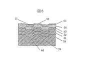
この媒体は次のようにして製作された。まず、図6に示すとおり、直径12cm、厚さ0.6mmで表面にトラックピッチが0.45ミクロンで深さ23nmのイングルーブ記録(ここでは光スポットから見てランド記録)用のトラッキング用の溝(幅0.25ミクロン)を有し、溝のウォブルによってアドレスが表現されたポリカーボネイト基板57上に、(In2O3)90(SnO2)10の組成の透明電極(ITO)52を膜厚30nmに形成した。基板表面への溝パターンの転写は、原盤のフォトレジストにメッキしたニッケルマスターから一度転写したマザーを用いて行った。フォトレジストに露光した溝がランドに対応するようにするためである。図6は基板上に製膜してゆくプロセスを示しているので、図4および図5とは上下が逆になっているので注意。さらに光導電体層であるAs3Se97の層52を厚さ50nmに形成した。次にGe−Sb−Te記録層54を平均膜厚10nmに形成した。この透明電極はマスクをしてスパッタリングで形成することにより、記録セクターに対応して放射状の20の領域に分離されている。次に絶縁層55であるSiO2層を120nm形成した。次に図6の最上部に示したようにアクリル樹脂層56を平均膜厚25nmに塗布し、波長254nmの紫外光を照射してランド部上の相対的に薄い樹脂層が無くなるまでエッチングした。この後、リアクティブイオンエッチングを行うと、ランド部上のSiO2層を除去し、記録層53を露出させることができた。すなわち、絶縁層に貫通する開口部を作ることができた。このように一部の層の膜厚をランドとグルーブで変えてランドとグルーブの一方で記録感度を高くし、トラッキングやAFズレに対する許容度を高めることは、電圧印加を行わず、光だけで記録する記録媒体の場合も効果が有る。次に、アクリル樹脂をプラズマアッシャーでほぼ完全に除去した。このようにして、図3の構成を得た。本実施例の記録媒体では絶縁層の有り無しで電極間に挟まれた部分の総膜厚に2倍以上の差が有り、SiO2層の抵抗値は他の層の抵抗値より大きいので、電極間の全層の抵抗値は開口部と開口部以外の部分で1:2以上の比となっている。記録層が相変化記録層である場合には、既知の、Ge2Sb2Te5、Ge5Sb70Te25などのGe−Sb−Te系記録材料や、Ag−In−Sb−Te系記録材料を用いた。記録層が実施例2で詳しく述べるポリチオフェン系などのエレクトロクロミック材料であってもよい。次にW80Ti20膜よりなる反射層兼第2の電極層45を膜厚50nmに形成した。積層膜の形成は、マグネトロン・スパッタリング装置を用いて行った。
【0034】
透明電極のシート抵抗の影響や、グルーブの凹凸の角の部分で透明電極に膜厚の薄い部分ができることの影響で、外周部に電圧がかかりにくくなることを防ぐために、基板上に透明電極を付ける前に、放射状透明電極より幅の狭い、半径方向の平均の幅が約100ミクロン、膜厚50nmから200nmの内周から外周に向かう細い金属(AlやAgが好ましい)電極39,40を、各放射状透明電極について1本または2本ずつ設けるのが、より好ましい。この電極は、記録媒体にマスクを付けてスパッタリングによって形成した。記録・再生はこの電極の部分を避けて行う。
【0035】
本実施例とは逆に光スポットから見てグルーブに見える状態で記録するには、透明電極と反射層兼電極を逆にし、張り合わせ基板側から光を入射させればよい。この場合、基板の成形はマザーでなく、ニッケルマスターを用いて行った。またこの場合、張り合わせ基板を0.1mm程度に薄くして、絞込みレンズのNAを0.85と大きくしても良い。そうすればトラックピッチは約3/4の0.33ミクロン程度にできる。
【0036】
なお、ここでは、光導電体層を用いた例を示したが、記録膜が光導電体層を兼ねる場合には、光導電体層を設けず、例えばエレクトロクロミック材料層一層あるいは相変化記録層一層でも良い。このような場合、絶縁層も必要無く、断面構造は図2に示したようになる。エレクトロクロミック材料層については実施例2で詳しく述べるが、ここではポリチオフェン系材料を用いた。実施例2で述べる他の材料も使用可能である。エレクトロクロミック材料層は実施例2で詳しく述べるように中味は3層からなっており、塗布または真空蒸着または電界重合で付けるが、そのうち少なくとも分子量の比較的大きいポリマー層は塗布によって形成するので、図2からわかるように基板のランド部では膜厚が薄くなり、グルーブ部では厚くなる。エレクトロクロミック材料層は透明電極層と電極層との間に電圧をかけることによって発色するが、ランド部の方が電極間距離が小さいため早く発色する。電圧を印加してランド部が発色し、グルーブ部はまだ十分発色しない時間後、電圧を切るか、電圧を下げて発色が進まず、状態をほぼ維持する低い電圧に制御すると、ランド部だけ光吸収が大きいので、記録時や読出し時にディスク回転数が速いなどの理由でトラッキングオフセットが生じても、記録や読出しはほぼ正確に行えるという効果が有る。
【0037】
なお、記録層と光導電体層との間には相互拡散・反応を抑制するため、導電体層(金属層や透明電極層)を極めて薄く設ければ、繰返し書換え時に信頼性が増す。ただし、光導電体層で発生したフォトキャリアが突き抜けるように、1nm以上10nm以下の平均膜厚にする必要がある。縞状や網目状の不連続膜であっても良い。例えば記録層と光導電体層との間に厚さ5nmのW80Ti20電極層を設けると、界面での電位の均一化、書換え時の記録層と光導電体層との間での相互拡散を防止して書換え可能回数を1桁向上させることができた。
【0038】
透明電極は複数の扇形透明電極に分離せず、ディスク全体が一電極でもよい。ただし、分離した方が電極間容量が小さくなるので、電圧の立上り、立下りが早くなって好ましい。発色、消色に要する時間と電流が実用的な範囲であるために電極間容量は0.1F以下が特に望ましいが、素子の特性が良好であるためには、0.01F以上となる構造とするのが良い。透明電極は複数の扇形電極に分離せず、金属電極の方を分離してもよい。また、上下の両電極を分離してもよい。この場合、上下の電極の切れ目の位置は一致していても良いが、一致していなくてもよい。
【0039】
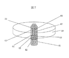
反射層兼電極と上記透明電極には、それぞれの最内周部に引き出し電極を設け、この引出し電極はディスク最内周部まで達しており、図4に示すように、記録再生装置のディスク回転軸上のそれぞれ別の電極に接続するため、ディスク中心穴の端面の複数の電極35、36に接続されている。図7に示したように、ディスク受け用円板68を貫通するディスク回転モーターの回転軸61の側面のディスクがセットされる高さの部分には、実施例2で述べるような多層ディスクの場合5層までに対応できるように6個の分離した電極が接着されており(図では電極6個中3個65、66、67を示している)、また、回転軸の円周上の一ヵ所では上下方向にテーパーのついた突起70または凹部があり、ディスクの中心穴の一ヵ所の凹部または凸部とのはめ合いで位置決めでき、所定の電極同士が接触する。ディスク回転軸の各電極には複数のブラシとリング62,63,64との組み合わせにより、記録装置の回路基板より給電される。給電方法は他の方法を用いても良い。
【0040】
なお、上記ディスク部材の膜表面には紫外線硬化樹脂を塗布して、,同じ形状のもう一枚の基板と貼り合わせ、ディスク状情報記録媒体を得た。
【0041】
また、記録・再生レーザー光は、基板側から入射させた。最後に付ける電極層を透明電極とし、透明電極側、すなわち張り合せ基板側からレーザー光を入射させても良い。ただし、この場合、反射率が約10%となり、読出しのコントラスト比が得られるように記録膜膜厚を決めた。
【0042】
(初期結晶化)
前記のようにして製作したディスクの相変化記録層には次のようにして初期結晶化を行った。ディスクを回転させ、スポット形状が媒体の半径方向に長い長円形の半導体レーザ(波長約810nm)のレーザ光パワーを800mWにして基板28を通して記録層24に照射した。スポットの移動は、媒体の半径方向のスポット長の1/4ずつずらした。こうして、初期結晶化を行った。この初期結晶化は1回でもよいが2回繰り返すと初期結晶化によるノイズ上昇を少し低減できた。
【0043】
(記録・消去・再生)
上記記録媒体に対して、情報の記録再生を行った。以下に、図9を用いて、本情報記録再生の動作を説明する。まず、記録再生を行う際のモーター制御方法としては、記録再生を行うゾーン毎にディスクの回転数を変化させるZCAV(Zoned Constant Linear Ve1ocity)方式を採用したものについて述べる。
【0044】
記録装置外部からの情報は8ビットを1単位として、8−16変調器8−8に伝送される。情報記録媒体(以下、光ディスクと呼ぶ)8−1上に情報を記録する際には、情報8ビットを16ビットに変換する変調方式、いわゆる8−16変調方式を用い記録が行われた。この変調方式では媒体上に、8ビットの情報に対応させた3T〜14Tのマーク長の情報の記録を行っている。図中の8−16変調器8−8はこの変調を行っている。なお、ここでTとは情報記録時のクロックの周期を表している。ディスクは光スポットとの相対速度が15m/sの線速度となるよう回転させた。
【0045】
8−16変調器8−8により変換された3T〜14Tのデジタル信号は記録波形発生回路8−6に転送され、マルチパルス記録波形が生成される。
【0046】
この際、記録マークを形成するためのパワーレベルを5mW、記録マークの消去が可能な中間パワーレベルを2mW、パワーを下げたパワーレベルを0.1mWとした。記録マーク形成のレーザーパワーは、印加電圧を上げてゆくと下げることができ、0.5mW以上5mW以下の範囲で良好な記録が行えた。線速度を15m/sから変えても、この範囲に大きな変化は無かった。読出しは、電圧を印加せずに1mWで行う。0.2mW以上2mW以下の範囲で実用的な読出しが行えた。2mWを越えるパワーで長時間読むと、記録されているデータの劣化が生じた。また、上記記録波形発生回路内において、3T〜14Tの信号を時系列的に交互に「0」と「1」に対応させるようにしている。この際、高パワーレベルのパルスが照射された領域は非晶質(マーク部)に変化する。また、上記記録波形発生回路8−6内は、マーク部を形成するための一連の高パワーパルス列を形成する際に、マーク部の前後のスペース部の長さに応じてマルチパルス波形の先頭パルス幅と最後尾のパルス幅を変化させる方式(適応型記録波形制御)に対応したマルチパルス波形テーブルを有しており、これによりマーク間に発生するマーク間熱干渉の影響を極力排除できるマルチパルス記録波形を発生している。
【0047】
記録波形発生回路8−6により生成された記録波形は、レーザー駆動回路8−7に転送され、レーザー駆動回路8−7はこの記録波形をもとに、光ヘッド8−3内の半導体レーザーを発光させる。
【0048】
本記録装置に搭載された光ヘッド8−3には、情報記録用のレーザービームとして光波長400nmの半導体レーザーが使用されている。また、このレーザー光をレンズNA0.65の対物レンズにより上記光ディスク8−1の記録層上に絞り込み、レーザービームを照射することにより情報の記録を行った。
【0049】
また、相変化記録層の場合、媒体の反射率は結晶状態の方が高く、記録され非晶質状態になった領域の反射率が低くなっている。レーザー光照射による記録の間、記録層の上下の電極間には5ボルトの電圧が継続的に印加される。パルスレーザー光照射によって、光導電体であるSe−Asの層にはフォトキャリア(電子、正孔対)が発生し、電気抵抗が低下するので、この部分の記録層にかかる電圧が増大し、記録層中に電流パスが形成され、電流のジュール熱によって記録層に融点を越える領域が形成される。融解後、この領域は電気抵抗が増大するので電流パスが消滅し、冷却されて非晶質状態になる。これによって記録層の屈折率と消衰係数も変化するので、光学的に信号を読出し可能である。情報信号に従ってこのパルスレーザー光照射を繰り返してゆけば、非晶質記録マーク列が形成される。記録を高速で行うと、レーザー光照射位置は高速で移動して行き、図8に電流の時間的変化を示したように、照射後も記録層が融解して高抵抗になるまで電流は流れ続けるので、複数の場所に同時に電流が流れ、先に流れ始めた場所から順次電流が止まって行く。
【0050】
このようなメカニズムで記録が行われるので、光スポットの通過時間は記録トラックの半径によって異なるが、電流が流れる時間は半径によらずほぼ一定になる。従って、通常相変化光ディスクでは難しい一定回転数(CAV)での記録が容易である。分離した透明電極には、光スポットが照射されている領域の電極に順次電圧を印加してゆく。
【0051】
高感度であるから複数光スポット同時記録ができ、また、光吸収量が少なくてよいので高反射率あるいは高透過率にでき、読出しが高S/Nで行える。また、読出し時には電圧を印加しないようにすれば、高い読出しパワーで読出しができるので高いS/Nが得られる。
【0052】
本実施例の記録媒体構造では、グルーブの部分だけで上下の電極が近接しているため、記録膜に高電界がかかる範囲が狭い。従って、光スポットの位置や集光度が多少変わっても同じように記録され、AF,トラッキングのズレに寛容で、光に対して高感度であるだけでなく、この面でも高速回転記録に適している。
【0053】
本実施例の記録媒体では、記録マークとそれ以外の部分とで約2:1の光反射率のコントラスト比が得られた。コントラスト比がこれ以下になると、再生信号のノイズによる揺らぎが上限値の9%を越えてしまい、実用的な再生信号品質の範囲を外れる。透明電極にSiO2を含有させて(SiO2)40(In2O3)55(SnO2)5とすると、屈折率が低下して光学的に有利になり、コントラスト比は2.5:1以上にできた。
【0054】
上記のような記録原理であるから、同一、または別々の記録トラックに、単一の光ヘッドからまたは複数の光ヘッドから複数の光スポットを形成し、同時に記録することも容易に行える。
【0055】
消去は、印加電圧を下げ、レーザー光を連続照射することによって非晶質領域を結晶化させて行う。消去もパルスレーザー照射を行い、どの記録パルスよりも広いパルスを繰りかえして消去しても良い。
また、本記録装置はグルーブとランドのうちランドに情報を記録する方式(いわゆるイングルーブ記録方式の変則版)に対応している。
【0056】
記録された情報の再生も上記光ヘッドを用いて行った。レーザービームを記録されたマーク上に照射し、マークとマーク以外の部分からの反射光を検出することにより、再生信号を得る。この再生信号の振幅をプリアンプ回路により増大させ、8−16復調器8−10では16ビット毎に8ビットの情報に変換する。以上の動作により、記録されたマークの再生が完了する。
以上の条件でマークエッジ記録を行った場合、最短マークである3Tマークのマーク長は約0.20μm、最長マークである14Tマークのマーク長は約1.96μmとなる。記録信号には、情報信号の始端部、終端部に4Tマークと4Tスペースの繰り返しのダミーデータが含まれている。始端部にはVFOも含まれている。
【0057】
(マークエッジ記録)
DVD−RAMおよびDVD−RWには高密度記録が実現できるマークエッジ記録方式が採用されている。マークエッジ記録とは、記録膜に形成する記録マークの両端の位置をディジタルデータの1に対応させるもので、これにより、最短記録マークの長さを基準クロック1個でなく2〜3個分に対応させて高密度化することもできる。DVD−RAMでは8−16変調方式を採用しており、基準クロック3個分に対応させている。マークエッジ記録方式は、円形記録マークの中心位置をディジタルデータの1に対応させるマークポジション記録に比べると、記録マークを極端に小さくしなくても高密度記録できるという長所がある。ただし、記録マークの形状歪みが小さいことが記録媒体に要求される。
【0058】
(ZCLV記録方式、CAV記録方式)
相変化記録媒体では、記録波形を変えない場合、良好な記録再生特性を得るのに結晶化速度に対応した最適線速度で記録するのが望ましい。しかし、ディスク上の半径の異なる記録トラック間をアクセスする時、線速度を同じにするために回転数を変えるのには時間がかかる。そこでDVD−RAMでは、アクセス速度が小さくならないようにディスクの半径方向を24のゾーンに分け、ゾーン内では一定回転数とし、別のゾーンにアクセスしなければならない時だけ回転数を変えるZCLV(Zoned Constant Linear Velocity)方式を採用している。この方式では、ゾーン内の1番内周のトラックと一番外周のトラックで線速度が少し異なるので記録密度も少し異なるが、ディスク全域にわたってほぼ最大の密度で記録することができる。
【0059】
一方、半径方向に大きくアクセスしても回転数を変えなくても良い点では回転数一定のCAV記録方式が好ましく、回転数を変える際の電力消費を抑制できるのでモバイル機器にも適している。本発明は既に述べたように半径方向位置によらず一定の加熱時間が得られるので、CAV記録も容易にする効果が有る。
【0060】
再結晶化の防止も重要である。記録時の記録膜融解後の周辺部からの再結晶化で非晶質記録マークとして残る部分が狭まる場合は所定の大きさの記録マークを形成するのにより広い領域を融解させる必要が有り、隣接トラックの温度が上昇しやすくなるからである。本発明では透明電極の熱伝導率が低いので、面内方向の熱拡散が少なく、再結晶化も防止できる。記録マーク形成時に中央部の熱が横方向に拡散して融解領域周辺部の冷却が遅くなり、結晶化しやすくなるのを防げるからである。
(トラッキング余裕)
本実施例では、ランド部では上部電極と記録膜が直接接しており、グルーブ部では間に絶縁層であるSiO2層が入っているので、ランド部とグルーブ部の電極間距離の比は60:180、すなわち1:3である。通常はディスクの内径、外径の偏心によりトラッキングオフセットが発生し、回転数を上げるほどオフセットが大きくなるが、本発明の場合、ランド領域だけで電極・記録膜が接するか、発色が起き、発熱が大きくなる構造であるから、記録のオフセットは縮小された。電極との間に界面層を設ける場合は、例えば界面層の厚さを5nmとすると、ランド部とグルーブ部の電極間距離の比は、65:145である。距離の比と、トラッキングオフセットが通常の上限値を越えてトラックピッチの1/10のとき、隣接トラックの既記録領域が部分的に消去されて信号レベルが低下してしまうクロスイレーズとの関係は、図10に示したように以下の通りである。
電極間距離の比 信号レベル低下量
1:3 −0.1dB
1:1.5 −0.5dB
1:1.4 −1dB
1:1.3 −2dB
1:1.1 −3dB
1:1.05 −4dB
上記から、距離の比は1:1.1以上であるのが好ましく、1:1.4以上であればさらに好ましい。また、電圧印加を行わず高パワーの光照射だけで記録する場合も同様な効果が有った。
【0061】
(記録層)
記録層材料としては、Ge2Sb2Te5,Ge4Sb2Te7、Ge5Sb70Te25などの組成のGe−Sb−Te系材料や、Ag4In6Sb65Te25などの組成のAg−In−Sb−Te系材料など、光ディスクで知られている各種材料が、要求される記録速度や他の特性に応じて使用可能である。記録メカニズムは、相変化のほか、多数回書換え可能ではなくなるが、記録層(エレクトロクロミック材料層や相変化材料層など)自身の穴形成や、発色能の破壊、色の変化、隣接する光導電体層や基板の変化・変形でも良い。
【0062】
多数回書換えが要求されない用途には有機材料も使用可能であって、実施例2で詳しく述べる各種有機導電性材料や、CD−R,DVD−Rで用いられる必ずしも導電性の高くない色素や、フォトクロミック色素やその他の既知の色素が使用可能である。これらの場合、記録メカニズムとしては、光および/または電流の作用による有機材料自身および/または光導電体層および/または基板表面の構造変化による光学的変化、または穴形成を利用する。導電率が高くない材料の場合は、最初から膜に顕著な穴があかない範囲で膜厚を薄くする必要がある。
【0063】
(光導電体層)
光導電体層としては、上記のAs−Se系材料のほか、高温熱処理が必要なため基板材質が制約されるがCdTe,CdS,CdSeなどの既知の無機光導電性材料、実施例2で詳しく述べるポリチオフェンなどの既知の各種有機導電性材料も、着色した状態で光導電材料として使用することができる。
(界面層)
結晶核形成速度と結晶成長速度を増大させ、結晶化速度を速くさせるために、好ましくは、記録膜と電極との間に、界面層を設ける。界面層の材料としては,下記より成るグループ、すなわち、Ta2O5などのTa酸化物、Cr2O3などのCr酸化物、Al2O3などのAl酸化物,SiO2などのSi酸化物,GeO2などのGe酸化物,SnO2などのSn酸化物,ZrO2などのZr酸化物,Co,Niの酸化物、Cr,Ge,Ti,Al,Si,Ta,Zr,B,Hfの窒化物うちの、単独、または2者以上の混合物,が好ましい。この中で、Cr2O3は多数回書き換え時の反射率レベルの変動を5%以下に押さえられ、ジッターを減少でき、より好ましい。CoO,Cr2O,NiOは初期結晶化時の結晶粒径が均一になり、書き換え初期のジッター上昇が小さくより好ましい。また,A1N,TaN,TiN,ZrN,BN,CrN,Cr2N,GeN,HfN,あるいはSi3N4、A1−Si−N系材料(例えばA1SiN2)、Al−Ti−N系材料,Si−Ti−N系材料,Si−O−N系材料や、これら窒化物の混合物も接着カが大きくなり、外部衝撃による情報記録媒体の劣化が小さく、より好ましい。また、Cr80Ge20などのCr−Ge系材料や、CrとGeの酸化物あるいは窒化物が60mo1%以上含まれていると保存寿命が向上し、高温高湿の環境におかれても高性能の記録媒体を維持できる。
【0064】
(電極材料)
電極材料として好ましいものは、用途によって異なる。多数回書換えを要求される場合は、タングステン、またはモリブデン、あるいはその少なくともいずれかを含み、チタンなどの他の金属元素を50原子%未満含むものが好ましい。
【0065】
一方、1回だけ記録する追記型や少数回の書換えでよい場合は、光学特性や熱拡散率を重視した、光ディスク用に好ましい金属を電極として用いるのが良い。反射率と熱伝導率が高い金属層は,AlあるいはAl合金の場合,Cr,Tiなどの添加元素が4原子%以下の高熱伝導率材料であるのが,基板表面の温度上昇を防止する効果があって好ましい。次いで,Au,Ag,Cu,Ni,Fe,Co,Cr,Ti,Pd,Pt,W,Ta,Mo,Sb,Bi,Dy,Cd,Mn,Mg,Vの元素単体、またはAu合金,Ag合金,Cu合金,Pd合金,Pt合金,Sb−Bi,SUS,Ni−Cr,などこれらを主成分とする合金、あるいはこれら同志の合金よりなる層を用いてもよい。このように、電極兼反射層は、金属元素、半金属元素、これらの合金、混合物、からなる。この中で、Cu,Ag,Au単体あるいはCu合金、Ag合金、特にPd,Cuなどの添加元素が8原子%以下のもの、Au合金等のように熱伝導率が大きいものは、有機材料の熱劣化を抑制する。透明電極の材料としては、(In2O3)x(SnO2)1−xの組成で、xが5%から99%の範囲の材料、抵抗値の面でより好ましくは、xが90%から98%の範囲の材料、これにモル%で50%以下のSiO2を添加したもの、SnO2にモル%で2から5%のSb2O3などの他の酸化物を添加したもの、などの既知の透明電極材料、および実施例2で詳しく述べるポリチオフェン、ポリアセチレンなどの導電性有機材料が使用可能である。
【0066】
(絶縁物層)
記録層の周辺の絶縁物層の融点は600℃以上であることが好ましい。600℃より融点が低い材料を絶縁物層として用いた場合、記録時に記録層で発生した熱及び絶縁物層自体による発熱により劣化し、光学特性が変化してS/Nが低下する場合がある。前記各層の膜厚,材料についてはそれぞれ単独の好ましい範囲をとるだけでも記録・再生特性等が向上するが,それぞれの好ましい範囲を組み合わせることにより,さらに効果が上がる。絶縁物層の材料としては、SiO2,Al2O3,Cr2O3,Ta2O5,GeO2、GeN,Si3N4、これらの組成比が異なるものなど、多くの酸化物、窒化物が使用可能である。絶縁性の有機材料を用いても良い。
【0067】
絶縁物層や光伝導体層や記録層を真空蒸着や塗布、特に塗布で形成する有機材料とした場合、ランドとグルーブの絶縁物層に膜厚差を付けるプロセスを用いなくても層を形成しただけで電極間距離に差ができ、電流集中の効果を得ることができる。
【0068】
(基板)
本実施例では、表面に直接、トラッキング用の溝を有するポリカーボネート基板77を用いているが、トラッキング用の溝を有する基板とは、基板表面全面または一部に、記録・再生波長をλとしたとき、λ/15n(nは基板材料の屈折率)以上の深さの溝を持つ基板である。溝は一周で連続的に形成されていても、途中分割されていてもよい。溝深さが約λ/12nの時、トラッキングとノイズのバランスの面で好ましいことがわかった。また、その溝幅は場所により異なっていてもよい。溝部とランド部の両方に記録・再生が行えるフォーマットを有する基板でも、どちらか一方に記録を行うフォーマットの基板でも良い。グルーブのみに記録するタイプでは、トラックピッチが波長/絞込みレンズのNAの0.7倍付近、グルーブ幅がその1/2付近のものが好ましい。
【0069】
(記録レーザパワー)
本実施例の記録媒体では、記録時に電流を流すことによって、記録媒体に低いレーザーパワーで記録できる。例えば、記録線速度15m/s以上の条件では、通常の記録媒体では記録レーザーパワーが10mWを越えるが、記録レーザーパワーを0.2mW以上2mW以下に設定することができる。最適記録パワーは、流す電流の値によって異なる。
【0070】
(読出しレーザパワー)
一方、本発明では、レーザーのパワーには余裕が有り、記録密度を高めても良好な再生信号S/Nを得たい場合には読出し時に読出しレーザパワーを高くしてレーザーノイズやシステムノイズの影響を受けにくくすることもできる。本実施例の記録媒体では、記録時に電流を流すことによって、記録層の光吸収が少ない、あるいは熱拡散が大きくて低い記録感度の記録媒体に記録できるので、読出し時に読出しレーザパワーを高くしても記録状態の読出し破壊が起きにくいためである。例えば、記録レーザーパワー2mWで読出しレーザーパワーを3mWにすることもできる。
【0071】
レーザー光源に、例えば4素子のアレーレーザーを用いた場合、データ転送速度を4倍近く高速化することができた。
【0072】
<実施例2>
本実施例は多層構造記録媒体およびそれを用いる記録装置に関するものである。
【0073】
図16に、本実施例の場合の記録装置の回転軸付近の構造を示した。図15に回路のブロック図を示したように、記録装置からは、回転軸の3本のスリップリング72,73,74に、プラスとマイナスの電圧と、記録媒体の層の選択信号が供給される。記録する時間に比べ発色・消色させる時間は短いので、一たんコンデンサーに充電することによって、高速発色・消色させる場合も記録装置の回路基板から回転軸への給電最大電流が少なくて済む。コンデンサーを含む図15の回路はディスク受け部品78の中空内部に内蔵されており、印加電圧切替え・制御回路を経て回路ブロック図の右端の各層への配線は、回転軸の電極75,76,77に接続されている。電極は8本有るが、他の5本は回転軸の見えていない面にあるので省略してある。これにより、発色させるべき層にはプラス電圧、消色する際にはマイナス電圧が印加される。記録装置の回路基板から回転軸への給電はプラス電圧だけにして、ディスク受け部品内蔵の回路で正負の電圧を生成しても良い。
【0074】
記録媒体は、実施例1と基本構造は同じであるが、記録層には、電圧印加により発色するエレクトロクロミック材料を用いる。図11に示したように、直径12cm、厚さ0.6mmで表面にトラックピッチが0.45ミクロンで深さ23nm、溝幅0.23ミクロンのイングルーブ記録用のトラッキング用の溝を有し、アドレス情報を上記溝のウォブルとして有するポリカーボネート基板89上に、Ag94Pd4Cu2半透明反射層81、ITO透明電極82、エレクトロクロミック材料層83、ITO透明電極84、ZnS・SiO2熱絶縁層85、ITO透明電極86、エレクトロクロミック材料層87、ITO透明電極88、ZnS・SiO2熱絶縁層、ITO透明電極、エレクトロクロミック材料層、ITO透明電極、ZnS・SiO2熱絶縁層、ITO透明電極、エレクトロクロミック材料層、ITO透明電極の順にエレクトロクロミック材料記録層を4層積層した。さらにこの上に直径120mm厚さ0.6mmのポリカーボネート基板90を貼り付けた。光はこの張り合せ基板側から入射させた。エレクトロクロミック材料層は3層または2層より成り、3層の場合、酸化発色型第1発色層であるIrOxまたはNiOx(xは1未満の正の数)の層150nm,固体電解質層であるTa2O5の層300nm,還元発色型第2発色層であるWO3の層200nmの3層、2層の場合、Cr2O3より成るOHイオン貯蔵層200nm、WO3より成る発色材料層200nmの2層である。なお、光入射側から最も遠い透明電極の代わりにW−Tiなどの金属電極を用いてもよい。エレクトロクロミック材料層を塗布によって形成する場合、積層によって少しずつグルーブが埋まり、記録層の両側の電極間距離はランド部の方がグルーブ部より近いが、実施例1のように1方の電極がほぼ平らになる程に、また、いずれかの層が貫通開口を持つ絶縁物層となるほどに電極間距離に差をつけてはいない。
【0075】
上記積層膜の上に紫外線硬化樹脂によるオーバーコート層を形成し、同様なもう1枚のディスクと張り合わせた。
【0076】
波長400nmのレーザー光を照射しながら、記録または読出しをしたい記録層の両側の透明電極に電圧を印加すると、その層だけが着色し、レーザー光を吸収、反射するようになるので、選択的に情報の記録や読出しができる。電圧印加は必ず1つの記録層だけに限定する必要は無く、アレーレーザーで複数記録層に同時に記録する場合は、複数対の電極間に電圧を印加する。また、記録しない記録層の電極間の電圧を0にしないで有限の値にしておけば、電極間容量や着色する材料の応答速度により、着色に時間がかかるのを防ぐことができた。また、電圧を除去して消色させる場合逆電圧を印加すると、消色に要する時間を1/2以下に短縮することができた。
【0077】
記録はレーザー光、および/または電流の作用によって、膜のエレクトロクロミック作用を失わせ、電圧を印加しても発色しない、あるいは記録前と異なる吸収スペクトルを持つようにして行う。別の方法として、熱または電流による物理的変化(相変化など)、または化学変化(例えばLiイオンとの反応)によって屈折率、消衰係数のうちの少なくとも一方が変化する有機、あるいは無機材料の層を別の層として積層し、この層の変化によって記録を行ってもよい。例えば、相変化記録膜として、In50Se45Tl5の組成のものを用いると波長780nmあるいは660nmの光、特に波長780nmの光に対して透過率が高いので好ましい。記録時にはエレクトロクロミック材料層の光吸収によって間接的に加熱される。エレクトロクロミック材料層は材料によって大小が有るものの光導電性を持つので、フォトキャリアの電流による加熱効果も生じる。相変化記録層を設けた場合は、加熱により、記録膜は結晶化、あるいは非晶質化の相変化を起こす。相変化による屈折率変化がエレクトロクロミック層の着色時に特に反射率差として見えやすいように光学設計しておくことにより、多層の記録膜のそれぞれをほぼ独立に読み出すことができる。透明電極から透明電極までの光学的膜厚が読み出し光の波長に対してほぼ1波長分になるようにすると、どの記録層も光学的に等価となるので好ましい。
【0078】
電圧印加を複数層に同時に、あるいは順次行って記録時、および/または再生時に複数層が発色するようにしても良い。各層の透明電極から透明電極までの厚さを絞込みレンズの焦点深度程度の厚さにし、光吸収係数が奥の層ほど大きくなるように発色させると焦点位置を深さ方向に振って高密度記録するのに好都合である。また、各層の膜厚をもう少し薄くすると、ボリュームホログラム記録などに有利である。各層の光吸収係数をほぼ同じにして膜厚は薄くし、高パワー照射では奥の層まで、低パワー照射では入射側に近い層だけが記録されるようにして多値記録してもよい。記録時と再生時の各層の光吸収係数の分布を変えられるのも本発明の特徴である。記録時には、単層で測定した時の吸収率が光入射側から20%、30%、40%、50%と奥ほど大きくなるように各層への発色電圧印加時間を変え、再生時にはどの層も20%で均一とすると、Ag−Pd−Cu層で反射して来た光には各層の情報が均一に含まれるので好都合である。
【0079】
全積層をいくつかにグループ化し、例えば本実施例の場合では4層を2層ずつのグループにして同一グループのエレクトロクロミック層は同時に発色、消色させるようにすれば、
発色、消色に要する時間を短くすることができる。同一グループ内では上記のように光入射側から遠い層の方の光吸収率が高くなるように電圧や、エレクトロクロミック材料のアクリル系ポリマーなどでの希釈程度を調整すると、より良好な記録特性が得られる。
【0080】
発色・消色に要する時間が記録・再生速度の制約要因にならないようにする他の方法として、光入射側から見て奥の層から順次発色させ、消色は手前の層から順次消色させるのが有効である。このようにすれば、一つの層の発色中に隣接する層に電圧をかけ始めて発色を準備することができ、スピードアップできる。
【0081】
エレクトロクロミック材料層に用いる材料としては、WO3のほか、チオフェン系有機物のオリゴマーやポリマーなどの、代表的な例を図12に示した有機材料が使用可能である。特に、導電性有機材料が好ましい。ただし、チオフェン系分子の重合体の場合、レーザーの波長は660nmとし、トラックピッチは約2倍の0.6μmとした。チオフェン系材料の重合体は真空蒸着または電解重合によって形成する。電解重合では、モノマーとしてはチオフェン誘導体であるポリ(3−メチルチオフェン)を用い、支持電解質としてLiBF4,溶媒としてベンゾニトリルを用いる。
【0082】
層構成は、Helmut W. Heuer氏らの、Advanced Functional Materials vol.12, No.2 pp89-94 (Feb. 2002) 記載の、electrochromic Window Based on conducting Poly(3,4-ethylenedioxythiophene)-Poly(styrene sulfonate)の論文に着色制御窓ガラス材料として述べられている材料と層構成のうち、(CeO2)67(TiO2)33より成るイオン貯蔵兼暗電流ブロック層、アクリル系紫外線硬化樹脂にLiトリフレート(正式名Liトリフロロメタンスルフォネート,Li trifluorometanesulfonate:CF3SO3Li)と可塑剤を混合した材料の固体電解質層、およびPEDT/PSSの層、すなわちpoly(3,4 etylenedioxythiophene)とpoly(stylene sulfonate) との混合材料よりなる電子活性導電性ポリマー発色材料層の3層である。チオフェン系ポリマーの層を形成する前に、チオフェン系分子ポリマーの端部にシアノ基(−NC)、チオール基(−SH)、S−アセチル基(−SAc)のいずれかを付ける処理を行った。チオフェン系分子ポリマーの長手方向がなるべく膜厚方向に向いて、膜厚方向の電流が流れやすいようにするためである。有機固体電解質層としてはポリエチレンオキサイド−チオシアン酸カリウム系も好ましい。
【0083】
上記PEDT/PSS層の代わりに、Fei Wang 氏他著のMicromolecules vol.33 pp2083-2091(2000)のElectrochromic Linear and StarBranched poly(3,4-ethylenedioxychiophene-didodecyloxybenzene) Polymers の論文に記載されているエレクトロクロミック発色ポリチオフェン系ポリマー材料であるSPEBを用いると、発色・消色が速く、良好な特性が得られた。ポリマーの合成方法、膜の形成方法などは論文と同様であるが、電解質には上記固体電解質を用いた。
【0084】
固体電解質層と電子活性導電性ポリマー発色材料層は、チオフェン系ポリマー層を電界重合によって形成し、例えばLiトリフレートのようなドーパントを膜中に取り込んでしまうことにより、一層化することもできる。このような有機材料層を用いる場合のメリットは、導電性が有り、導電率は温度上昇とともに高くなり、また、光導電性も持たせることができるのでフォトキャリアーを電界によって加速し、温度上昇により記録感度を高めることができること、WO3のように発色消色に膜中への水分の出入りを必要としないことである。着色は分子中に電子が与えられることにより光で励起状態にできるようになることによって起こる。この電子移動を中和するためにLiなどのイオンが移動する。デメリットは、製膜速度が遅く、大面積の製膜が容易でないことである。この欠点を改良するため、モノマー、または数分子が結合しただけの低分子量のものを高速真空蒸着し、基板上でオリゴマーにするのが好ましい。基板上でオリゴマーにするには、真空蒸着中に青色または近紫外光を照射して分子を励起状態にする。チオフェン系ポリマー(略してポリチオフェン)のほか、Lu−ジフタロシアニンなどの金属フタロシアニン、ヘプチルビオロゲン、タングステン蓚酸錯体,スチリル系化合物である 3,3ジメチル-2-(P-ジメチルアミノスチリル)インドリノ[2,1−b]オキサゾリン(IRPDM)(光源波長5145nm)や3,3ジメチル-2-(P-ジメチルアミノシンナミリデンビニル)インドリノ[2,1−b]オキサゾリンなども使用可能である。
【0085】
さらに、光導電効果をもたせるために、TCNQ(7,7,8,8−Tetracyanoquinodimethane)の層を形成してもよい。
これら有機物を用いる場合も、ディスクの他の部分は上記実施例と同様とした。
【0086】
WO3に代わる無機物の材料としては鉄のシアン化物であるプルシャンブルー(KxFeIIyFeIIIz(CN)6、MoO3,Nb2O5,V2O5,TiO2,NiOOH,CoOOH,Rh2O3,IrOx(xは1未満の正の数)、ZrNCl,InN,SnNx(xは1未満の正の数)、MnOx(xは2未満の正の数),WO3−MoO3複合(混合)薄膜なども使用可能である。
【0087】
エレクトロクロミック材料では、電流によってLiなどの金属や水素などの陽イオンが所定の場所から動いてしまったり光スポット内の基底状態にある電子のほとんどが励起されてしまうと、自動的に光吸収が減ったり電流が流れにくくなるので、ディスク全体に大きな電流が流れたり、光スポット照射部分で過大な電流が流れて記録マークが大きくなりすぎるのが防止できる。すなわち現象としては、第1の電極と第2の電極との間に電圧を印加しながら光を照射すると、照射した場所付近の電流が増大し、光照射が終わってからも電圧を印加し続けた場合、一定時間後に電流が低下し、記録層(エレクトロクロミック層など)の状態変化が観測される。光照射中に自動的に電流が低下する場合も有る。
【0088】
エレクトロクロミック層の代わりにエレクトロルミネッセント(EL)材料とフォトクロミック材料の混合材料を用いても良い。EL材料が発する光によって、フォトクロミック材料の色が変化し、記録あるいは読出し光の波長に対して光吸収が生じるようにする。EL材料としてはZnOなどの無機材料や有機材料を用いることができるが、有機材料については、例えば豊田中央研究所R&DレビューのVol.33,No.2(1998年6月)の3ページから22ページの解説に述べられている有機EL材料のうち、ジアリルエテン、フルギドなどのフォトクロミック材料を変色させるのに発光波長が適合するものを当該フォトクロミック材料と組み合わせて用いる。これら有機材料の層の場合は、真空蒸着、気相成長、塗布などの方法で形成する。塗布の場合は溶媒で十分に希釈して、グルーブ部分とグルーブ間の部分で膜厚差が大きくなり過ぎないようにした。有機EL材料は電子またはホール輸送層材料と発光層材料と、効率を向上させたい場合はドーピング材料からなり、ホール輸送層材料としては、トリフェルアミンを星形分子にしたスターバーストアミン(m−MTDATA)膜厚60nm,発光層材料としてはベンゾオキサゾールZn錯体(Zn(BOX)2)膜厚40nmを用いて青色発光する。
【0089】
フォトクロミック材料としては、図12に示したフルギド、ジアリールエテンなどが使用できる。フルギドの場合、青色光照射によって波長500nm付近に吸収が生じるので、波長514.5nmのKrレーザーで記録可能である。
【0090】
シート抵抗が大きいことがあまり問題とならない小型の記録媒体では、透明電極もポリアセチレン、ポリチオフェンなどの導電性ポリマーで形成することが可能である。その場合、無機物透明電極に比べてエレクトロクロミック層との屈折率差が小さく、界面で反射した光の干渉などの悪影響を避けることができる点で好ましい。下地層として疎水性表面処理剤、シランカップリング剤、または平均0.5から3nmの膜厚の薄い銅族元素(Cu,Ag,Au)層を設けても良い。
【0091】
さらに、断熱層も有機材料とすれば上記と同じ理由で光学的に好ましい。断熱層は導電性が有っても良いが、無い方がより好ましく、アクリル系オリゴマー、ポリマー、金属フタロシアニンの真空蒸着膜など、多くの材料が使用可能である。
【0092】
この他、EPD、すなわち電気泳動表示媒体に使われる有機材料、または電流昇温で吸収端が変化する導電性有機材料層を用いてもよい。
【0093】
記録層に相変化材料層を用いても良い。例えばレーザー光源が赤色の場合、In−Se系、In−Se−Tl系などのSeを30原子%以上含む相変化記録層は光吸収が少なく、エレクトロクロミック材料層の光吸収による間接加熱および/または電流の作用で相変化する。相変化記録層は屈折率が高いので界面での反射を防ぐために透明電極層の膜厚を反射防止効果を持つように選ぶのが良い。
【0094】
多層膜はすべて絞り込みレンズの焦点深度内に有っても良いが、厚さ20〜40ミクロンのスペーサー層を数層毎(例えば3層おき)に挟んで焦点位置を変えて各層に記録・再生してもよい。この場合、スペーサー層を2層以上用いる場合は、光学系に球面収差を補償する素子を設けた方が良い。
【0095】
記録・再生方法などは実施例1と同様である。
【0096】
<実施例3>
本実施例では、図14に示したように、レーザー91の光93をミラー駆動モーター95の回転軸に対し直角より少し傾いた面で取り付けられ、高速回転するミラー94で方向が円または楕円運動するように反射され、MEMS技術の一つであるシリコン単結晶から形成した4×6の反射鏡アレー97によって光スポットを形成し、記録媒体を高速で移動させることなく高速度の記録を行う。なお、図中92はレンズ、96は列選択ミラー、98はSiウエハー、99は記録積層膜の断面である。全体の形状は円板状ではなく、長方形の形状とした。各ミラーは、その下部のトランジスタアレーにより、静電力または電磁力により駆動される。
【0097】
記録媒体の基板表面には、通常の光ディスクの原盤形成プロセスと同様にして縦、横に規則正しく配列したスリバチ状の多数の窪みを形成した。窪みの直径は1μm、深さは0.4μm、窪みの中心間の距離は1.5μmとした。窪みの基板に平行な面による断面形状は円形でなく少し楕円形でも良い。この基板上に、厚さ50nmの熱拡散用Ag94Pd4Cu2層、厚さ50nmのZnS・SiO2保護層、厚さ30nmのGe−Sb−Te記録層、厚さ50nmのZnS・SiO2保護層の4層をスパッタリングによって2回繰返し積層し、最後にAl98Ti2電極層を70nmの厚さに形成した。その上に紫外線硬化樹脂を挟んで厚さ100μmのポリカーボネートシートを貼り、紫外線硬化樹脂を硬化・接着した後シートを引き剥がすと、平坦部の積層膜は除去され、スリバチ部分だけに積層膜が残って、積層膜の断面99が露出した。この断面に記録を行うことができる。基板表面を紫外線照射によって活性化しておくと、積層膜の第1層のAg合金層だけは基板の平坦部上を含めて全体を基板上に残すことが可能で、電極として使用できる。断面99を露出させた後、厚さ30nmのSiO2層と厚さ70nmのITO透明導電膜を形成すると、窪みに落ち込む傾斜部ではSiO2層がほとんど付かず、透明導電膜が直接最上部の電極層に接するので、最下部のAg合金膜と最上部のITO層との間に電圧を印加して断面への光照射による記録を補助ことができる。また、上部の絶縁層と透明電極を付けない場合、断面の保護層を希酸で短時間エッチングした後、断面にTiO2層を厚く形成すると、TiO2層がカマボコ状の媒体作り付けソリッドイマージョン円柱レンズとなって、光を十分集光して記録層断面に照射することができる。
【0098】
Ge−Sb−Te記録層の代わりに、実施例2で述べたチオフェン系ポリマーまたはWO3系のエレクトロクロミック材料層の積層膜を設けても良好な特性が得られた。記録は、熱によりエレクトロクロミック材料層の発色能を破壊することによって行う。
【0099】
一方、基板表面に従来の光ディスクのようなグルーブを形成し、グルーブ上に記録を行うこともできる。グルーブは8本形成し、その方向は反射鏡アレーの配列方向と平行とした。反射鏡アレーの配列周期はグルーブの周期の2倍になっており、ミラーの角度を変えることによって2つのグルーブのいずれかに記録が行える。通常は一方のグルーブに記録した後、他方のグルーブに移って記録する。記録媒体は実施例2と同じ多層構造になっている。各層に使用する材料は実施例2で述べたように有機材料でも無機材料でも良い。グルーブは直線状でなく、各ミラーの下に同心円または螺旋状に設けても良い。
【0100】
上記のいずれの場合も、ミラーアレーでなく移動するミラーで各部分に照射しても良い。
【0101】
レーザー光源に、例えば4素子のアレーレーザーを用いた場合、上部の4つのミラーに同時にレーザー光を送ってデータ転送速度を4倍近く高速化することができる。
【0102】
反射鏡アレーは、大容量が要求される用途では1000×1000程度まで数を増すことができる。
【0103】
なお、記録・再生方法は、実施例1と同様である。
【0104】
【発明の効果】
本発明の情報記録媒体では、高電界が印加される範囲が狭いので、オートフォーカス,トラッキングのズレに寛容で高速回転が可能であり、高速記録、高密度記録が可能となる。
また、従来より大幅に多層化可能であり、実効的記録密度を上げ、記録媒体1枚あたりの記録容量を大幅に大容量化できる。
【図面の簡単な説明】
【図1】従来例の情報記録媒体の構成図である。
【図2】本発明の一実施例の情報記録媒体の断面図である。
【図3】本発明の他の一実施例の情報記録媒体の断面図である。
【図4】本発明の一実施例の情報記録媒体の1/4分割図である。
【図5】本発明の一実施例の情報記録媒体の1部を切り出したものの鳥瞰図である。
【図6】本発明の一実施例の情報記録媒体の絶縁層をエッチングする予備工程の記録媒体の断面図である。
【図7】本発明の一実施例の情報記録媒体をセットするディスクホルダー部分の電極を示す図。
【図8】本発明の情報記録媒体の1つの記録点に流れる電流の時間変化を示す図。
【図9】本発明の情報記録装置の構成を示す図。
【図10】電極間距離の比とトラッキングオフセットによる信号レベル低下量との関係を示す図。
【図11】本発明の多層ディスクの積層構造を示す図。
【図12】有機エレクトロクロミック材料の例の分子構造を示す図。を示す図。
【図13】有機フォトクロミック材料の例の分子構造を示す図。
【図14】本発明の実施例の情報記録媒体の構造および光学系を示す図。
【図15】本発明の実施例の印加電圧制御回路のブロック図。
【図16】本発明の一実施例の情報記録媒体をセットするディスクホルダー部分の電極を示す図。
【符号の説明】
1: 透明電極
2: UV樹脂レプリカ層
3: 保護層
4: 記録層
5: 保護層
6: 電極
7: 基板
8: 絞込みレンズ
9: レーザー光
10:DC電源
11:保護層
12:透明電極層(電極1)
13:エレクトロクロミック材料層
14:電極1
15:紫外線硬化樹脂層
16:張り合せ基板
17:基板
18:グルーブ部
19:ランド部
20:入射レーザー光
21:保護層
22:透明電極
23:光導電体層
24:記録層
25:絶縁体層
26:第1の電極
27:張り合せ基板
28:基板
29:グルーブ部
30:ランド部
31:張り合せ基板
32:積層膜
33,34:透明電極
35,36:透明電極からの引出し電極
37:ディスク中心
38:電極間スペース
39,40:細い金属電極
41:透明電極
42:光導電体層
43:記録層
44:絶縁体層
45:第1の電極
46:光スポット
47:グルーブ部
48:ランド部
49:電極間スペース
50:マルチビーム記録の場合の第2の光スポット
51:絶縁体層
52:透明電極
53:光導電体層
54:記録層
55:絶縁体層
56:塗布有機材料層
57:基板
58:ランド部の塗布が薄い部分
59:ランド部
60:グルーブ部
61:回転軸
62:第1のスリップリング
63:第2のスリップリング
64:第3のスリップリング
65:第1の接触電極
66:第2の接触電極
67:第3の接触電極
68:ディスク受け部品
69:絶縁体
70:位置決め用凸部
81:薄いAg合金反射層
82:透明電極
83:エレクトロクロミック層
84:透明電極
85:熱絶縁層
86:透明電極
87:エレクトロクロミック層
88:透明電極
89:基板
90:基板
91:レーザー
92:レンズ
93:レーザービーム
94:回転ミラー
95:ミラー駆動モーター
96:列選択ミラー
97:行選択ミラー
98:Siウェハー
99:記録積層膜の断面。[0001]
BACKGROUND OF THE INVENTION
The present invention relates to an information recording medium that records and reproduces information using light, an information recording method, and an information recording apparatus.
[0002]
[Prior art]
An optical disc is characterized in that the recording medium (disc) can be removed from the recording / reproducing apparatus and the recording medium is inexpensive. Therefore, it is desirable to increase the speed and density without losing this feature in the optical disc apparatus.
[0003]
There are various known principles for recording information by irradiating a recording film with light, but many of them utilize thermal atomic changes such as phase changes (also called phase transitions or phase transformations) of film materials. It has the advantage that a rewritable information recording medium can be obtained. For example, as described in Japanese Patent Application Laid-Open No. 2001-344807, the basic configuration of these phase change optical discs includes a protective layer, a GeSbTe-based recording film, a protective layer, and a reflective layer on a substrate.
[0004]
On the other hand, a field effect type optical disc is known in which information is recorded on a phase change recording film by irradiating a laser beam with an electric field applied to the recording film. This is used in an element structure in which a phase change recording layer such as a GeSbTe system is sandwiched between upper and lower electrodes. This field effect type optical disk is described in, for example, Japanese Patent Laid-Open No. 63-122202. It is intended that the phase change (crystallization) is promoted more than the laser light irradiation only by applying an electric field to the recording film. The configuration is shown in FIG. The light 9 is collected by the
[0005]
In addition, the present inventors' paper: M. Terao, H. Yamamoto and E. Maruyama: Highly Sensitive Amorphous Optical Memory: supplement to the J. of the Japan Society of Applied Physics Vol.42, pp233-238 An experimental result has been reported that when a conductor and a phase change recording film are sandwiched between transparent electrodes and light is applied while voltage is applied to the transparent electrode, recording can be performed with a laser beam that is nearly two orders of magnitude weaker than light irradiation alone. Yes. On the other hand, there are CD-Rs and DVD-Rs that have been put into practical use as optical disks using an organic material as a recording layer. These perform recording by altering the recording layer containing a dye having absorption at the wavelength of the recording light source and the substrate surface in contact with the recording layer by laser irradiation.
[0006]
[Problems to be solved by the invention]
Although speeding up is important, optical discs are characterized by the fact that the disc can be attached to and detached from the device and that the recording medium uses a plastic substrate and is inexpensive, so it is difficult to avoid vertical deflection and eccentricity of the outer periphery of the disc. . Since vertical shake and eccentricity become high frequency when the rotational speed is increased, it becomes difficult to follow autofocus and tracking. Therefore, in order to increase the speed beyond the limit of the mechanical vibration tracking of the apparatus, it is necessary that the recording medium is tolerant of tracking misalignment or the like particularly during recording which is easily affected.
[0007]
In the technique of the above-mentioned supplement to the J. of the Japan Society of Applied Physics Vol.42 by the inventors of the present application and the field effect medium described in JP-A-63-122032, both the land part and the groove part are used. Since almost the same voltage and the same light absorption are obtained, it is not easy to record only one of the land and the groove. Therefore, the tolerance for the tracking error is not large, and sufficient high-speed recording cannot be performed. On the other hand, CD-R and DVD-R have no substantial difference in light absorption between the land portion and the groove portion, and it is difficult to assist recording by current.
[0008]
An object of the present invention is to solve these problems and achieve stable large-capacity ultrahigh-speed recording.
[0009]
[Means for Solving the Problems]
The configuration of the present invention for solving the above problems will be described below.
[0010]
However, in the present invention, a portion that is a groove in the concave portion of the substrate is called a groove. The land between the grooves is called a land. When light is incident on the film through the substrate, the groove looks convex when viewed from the incident side. For this reason, even in a method in which light is incident from the side opposite to the substrate, the convex side when viewed from the incident side is sometimes called a groove. This part is a convex part when attention is paid only to the substrate, and is a land part between the grooves, so that the terminology is opposite to the definition of the present invention. In the case of so-called in-groove recording, in which recording is performed on only one of the land and the groove, the recording characteristics are better when the light incidence is from the substrate side or from the opposite side of the substrate and the recording is performed on the convex portion when viewed from the light incidence side. In many cases, it is good, but since it is not a large difference, it may be recorded in the recess as viewed from the light incident side.
The configuration of the present invention is specifically as follows.
(1) A structure in which a first electrode, an electrochromic material, and a second electrode are provided on a substrate, and the electrochromic material layer is colored in the first region, and the electrochromic material layer is not colored in the second region And Here, the first region corresponds to a land portion, and the second region corresponds to a groove portion, and light is absorbed only in the first or second region, so that a range that can be easily recorded is specified. Therefore, even if the position of the light spot and the light condensing degree are slightly changed, the same recording is performed, and a high-speed recording is possible with a tolerance for a shift in AF and tracking. Furthermore, high density recording can be achieved.
[0011]
Here, this configuration is shown in FIG. Here, for ease of understanding, the light is shown as incident from the upper side of the drawing. The medium is composed of a
[0012]
Alternatively, on the substrate, the first electrode, an insulating film having an opening penetrating on the first electrode, a recording film for recording information formed from the opening to the insulating film, and the recording The second electrode is formed over the film.In FIG. 3, since the surface of the
[0013]
Therefore, even if the position of the light spot and the light condensing degree are slightly changed, the same recording is performed, and a high-speed recording is possible with a tolerance for a shift in AF and tracking. Furthermore, high density recording can be achieved.
[0014]
A phase change recording layer (for example, a layer of Ge2Sb2Te5) may be provided between the electrochromic recording layer and the first or second electrode. It is optically more preferable to provide it on the side opposite to the light incident side. In this case, the electrochromic layer has a high recording threshold value, and the phase change recording layer is selected to have a low melting point containing sulfur such as Sb4Te3S2 so that recording occurs only in the phase change recording layer, or the electrochromic layer May be removed.
[0015]
(2) Further, as shown in FIG. 3, a
[0016]
However, the recording layer may also serve as a photoconductor layer, or the recording layer may be of a type whose electrical resistance is reduced due to temperature rise. A chalcogenide material such as Ge—Sb—Te or an organic conductive material such as polythiophene corresponds to a type in which the electrical resistance is reduced due to a temperature rise. In the figure, 21 is a protective layer, 22 is a transparent electrode, 25 is an insulator layer, and 26 is a second electrode.
[0017]
(3) In order to supply current to the first and second electrodes using a circular information recording medium, the first electrode is elongated in the radial direction of the information recording medium.OrA third electrode for supplying current to the second electrode is preferably provided. When the third electrode is provided in this way, the same voltage can be applied to the outer periphery.
[0018]
(4) Light may be applied while applying a voltage between the first electrode and the second electrode, and the voltage may be applied even after the light irradiation is completed. When light is applied while applying a voltage between the first electrode and the second electrode, the current in the vicinity of the irradiated location increases as shown in FIG. If the voltage continues to be applied even after the light irradiation is completed, the current automatically decreases due to the decrease in excited carriers, the melting of the recording film itself, the increase in resistance due to disorder and decomposition of the atomic / molecular arrangement, After returning to the current value, a change in the state of the recording layer is observed. As a result, in the case of a disk-shaped medium, the energization / heating time for recording is almost the same on both the inner and outer circumferences, so that it is easy to adapt to CAV (constant angular velocity) recording. Further, it is possible to prevent the current from flowing through the entire recording medium to become a large current, and the current cannot be supplied, and the change in the state of the recording film and the damage area from becoming excessively large. For this purpose, the apparatus may be provided with a control circuit that suppresses the applied voltage to 80% or less of the voltage at which recording occurs only by the voltage.
[0019]
(5) Of the first electrode and the second electrode, at least one of the electrodes may be divided into a plurality of parts. If it is divided radially, it is easy to adapt to CAV (constant angular velocity) recording, and the interelectrode capacitance can be reduced, so that the response speed can be improved.
[0020]
(6) The present invention is also suitable for multilayer recording in order to further improve the recording density.. FruitIn order to increase the effective recording density (effective surface density), multilayering is desirable,In conventional media, eachLayer transmittance and recording sensitivity are in a trade-off relationship,With more than 3 layersEither playback signal quality or recording sensitivity must be sacrificed. It is also known that three-dimensional recording is performed on the transparent organic material including the thickness direction, but the recording sensitivity is very poor when using two-photon absorption, and the storage stability and recording sensitivity when using photopolymerization. Is bad.
[0021]
However, in the present application, since two or more recording layers are provided and the recording layers other than the recording layer farthest from the light incident side are sandwiched on both sides by the transparent electrodes, the transmittance of each layer is increased, so that the recording sensitivity is also reproduced. Both quality can be improved.The recording layer farthest from the light incident side may be sandwiched between transparent electrodes on both sides, or may not have such a configuration.
[0022]
In the case of multi-layer recording having two or more recording layers, the recording layer other than the recording layer farthest from the light incident side has a recording or reading laser beam absorptance when a voltage is applied between the electrodes sandwiching the recording layer. It is preferable to increase it.The recording layer farthest from the light incident side may have an increased absorptance or may not have such a configuration.Thereby, since there is no interference of other layers, all the layers can be arranged within the focal depth of the focusing lens, and the multilayer and the capacity can be increased as compared with the conventional multi-layer disc. For this purpose, an organic or inorganic electrochromic material or a mixed material layer of an electroluminescent material and a photochromic material or a laminated film may be used as the recording layer or a layer adjacent to the recording layer. Thereby, only an arbitrary layer can absorb light, and the other layers can hardly absorb light. Of course, some layers may not be within the focal depth, and recording / reproduction may be performed by moving the focal position. In that case, there are cases where pits and grooves representing address information are deformed when multi-layered, but depending on the case, by providing a layer to which the pits and grooves are transferred again, at least a part of the depth of focus within the focal depth at the moved focal position. It is necessary to be able to read the address of the layer. Examples of the electrochromic material include tungsten oxide and thiophene organic molecule polymers.
[0023]
Furthermore, as the electrochromic material, many electrochromic materials that have been published at present are used, such as various materials described in "Electrochromic Display" published on June 28, 1991 by Sangyo Tosho Co., Ltd. Is possible.
[0024]
(7) During recording, the recording laser power can be set to 0.2 mW or more and 2 mW or less even when the recording linear velocity is 15 m / s or more for the medium (1). By increasing the sensitivity in this way, even in the case of high linear velocity recording, and when using an array laser or a surface emitting laser as a means for simultaneously irradiating light to a plurality of locations on the recording medium, power is insufficient. In addition, a high transfer rate can be realized. It is also possible to irradiate the erase region with pulsed light so that the pulse width is wider than the recording mark forming pulse. Thereby, even in the erasure area, the erasure width does not become too wide and good rewriting can be performed. A voltage may be applied to at least two pairs of electrodes of the recording medium simultaneously. This is necessary when a material that changes color unless a low sustaining voltage is applied.
[0025]
A recording medium having a plurality of recording layers is used, and a voltage is applied between many electrode pairs. However, at the time of recording, erasing, or reading, only the electrodes on both sides of the layer that performs them are different from the other electrodes. Alternatively, a different voltage may be applied.
[0026]
(8) As a device, a plurality of electrodes are arranged on a rotating shaft of a disk rotating motor or a portion of a disk receiving part attached to the rotating shaft and in contact with a disk center hole. Means for positioning so as to face each electrode and means for contacting the rotating shaft side electrode and the disk side electrode are provided. Thereby, a predetermined voltage can be applied to each electrode.
[0027]
In addition, at least one place in the circumferential direction of the rotating shaft of the disk rotating motor or the side of the disk receiving part attached to the rotating shaft, to which the divided electrode is added at the height portion where the disk is set The information recording apparatus is characterized in that a protrusion having a taper in the vertical direction is provided. As a result, the disk can be positioned in the rotational direction, and power can be accurately supplied to the multilayer electrodes.
[0028]
The present invention is effective when the recording density (track pitch, bit pitch) exceeds the standard of 2.6 GB DVD-RAM, and particularly effective when the recording density exceeds the standard of 4.7 GB DVD-RAM. . When the wavelength of the light source is not near 660 nm, or when the numerical aperture (NA) of the condenser lens is not 0.6, the effect is obtained at a recording density or more converted from the wavelength ratio and NA ratio in both the radial direction and the circumferential direction. Demonstrate.
[0029]
In this specification, not only a phase change between a crystal and an amorphous state but also a phase change between melting (change to a liquid phase) and recrystallization, and a phase change between a crystal state and a crystal state. The term is used.
[0030]
In addition, in the present invention, an electrochromic material layer is a layer of a material that directly develops color (absorption spectrum changes) when voltage is applied (current flows), and emits light when voltage is applied (current flows). And a layer having a region that develops and decolors by receiving the light.
[0031]
In addition, the electrochromic material of the present invention has conductivity that a current of 0.1 mA or more flows constantly when a voltage of 2 V is applied between the first and second electrodes of a disk having a diameter of 80 mm or more. It is defined by
[0032]
DETAILED DESCRIPTION OF THE INVENTION
<Example 1>
(Configuration, manufacturing method)
4 and 5 show the structure of the disc-shaped information recording medium according to the first embodiment of the present invention. FIG. 4 shows a quarter of the structure of the disk, and FIG. 5 further shows an enlarged view of a part thereof. There are many radial transparent electrodes in the upper part of FIG. 4 so that the same shape fills the disk surface, but only two of them are drawn. The recording / reproducing light is incident from above through the substrate, but the uppermost substrate is omitted in the figure. FIG. 5 shows an enlarged view of a part of the disk. Also in FIG. 5, the uppermost substrate and the insulating layer are omitted for easy understanding. In FIG. 5,
[0033]
This medium was manufactured as follows. First, as shown in FIG. 6, for tracking for in-groove recording (here, land recording as viewed from a light spot) having a diameter of 12 cm, a thickness of 0.6 mm, a track pitch of 0.45 microns and a depth of 23 nm. On the
[0034]
In order to prevent the voltage from being easily applied to the outer periphery due to the effect of the sheet resistance of the transparent electrode and the thin part of the transparent electrode at the corners of the concave and convex portions of the groove, the transparent electrode is placed on the substrate. Before applying, thin metal (Al and Ag are preferable)
[0035]
In contrast to the present embodiment, in order to record in a state that looks like a groove when viewed from the light spot, the transparent electrode and the reflective layer / electrode may be reversed and light may be incident from the bonded substrate side. In this case, the substrate was formed using a nickel master instead of a mother. In this case, the laminated substrate may be thinned to about 0.1 mm, and the NA of the focusing lens may be increased to 0.85. Then, the track pitch can be reduced to about 3/4 of 0.33 microns.
[0036]
In this example, the photoconductor layer is used. However, when the recording film also serves as the photoconductor layer, the photoconductor layer is not provided. For example, one electrochromic material layer or a phase change recording layer is provided. One layer is fine. In such a case, an insulating layer is not necessary, and the cross-sectional structure is as shown in FIG. The electrochromic material layer will be described in detail in Example 2. Here, a polythiophene-based material was used. Other materials described in Example 2 can also be used. As will be described in detail in Example 2, the electrochromic material layer is composed of three layers, and is applied by coating, vacuum deposition, or electric field polymerization. Among them, a polymer layer having a relatively high molecular weight is formed by coating. As can be seen from FIG. 2, the film thickness is reduced at the land portion of the substrate and thicker at the groove portion. The electrochromic material layer develops color when a voltage is applied between the transparent electrode layer and the electrode layer, but the land portion develops color earlier because the distance between the electrodes is smaller. When a voltage is applied and the land portion develops color and the groove portion does not yet develop enough color, when the voltage is turned off or the voltage is lowered and the color development does not progress and the voltage is controlled to a low voltage that substantially maintains the state, only the land portion is lighted. Since the absorption is large, there is an effect that recording and reading can be performed almost accurately even if a tracking offset occurs due to a high disk rotational speed during recording and reading.
[0037]
In addition, in order to suppress mutual diffusion and reaction between the recording layer and the photoconductor layer, if an extremely thin conductor layer (metal layer or transparent electrode layer) is provided, the reliability increases during repeated rewriting. However, an average film thickness of 1 nm or more and 10 nm or less is necessary so that photocarriers generated in the photoconductor layer penetrate. It may be a striped or network discontinuous film. For example, a 5 nm thick W between the recording layer and the photoconductor layer.80Ti20When the electrode layer was provided, the potential at the interface was made uniform, and mutual diffusion between the recording layer and the photoconductor layer at the time of rewriting was prevented, and the number of rewritable times could be improved by one digit.
[0038]
The transparent electrode is not separated into a plurality of fan-shaped transparent electrodes, and the entire disk may be a single electrode. However, it is preferable that the voltage is separated because the interelectrode capacitance becomes smaller, so that the voltage rises and falls faster. Since the time and current required for color development and decoloration are in a practical range, the interelectrode capacitance is particularly preferably 0.1 F or less. However, in order to have good device characteristics, the structure is 0.01 F or more. Good to do. The transparent electrode may be separated from the metal electrode instead of being separated into a plurality of sector electrodes. Also, the upper and lower electrodes may be separated. In this case, the positions of the cuts between the upper and lower electrodes may be the same or may not be the same.
[0039]
Each of the reflective layer electrode and the transparent electrode is provided with an extraction electrode at the innermost circumference, and this extraction electrode reaches the innermost circumference of the disk. As shown in FIG. In order to connect to different electrodes on the shaft, they are connected to a plurality of
[0040]
An ultraviolet curable resin was applied to the film surface of the disk member and bonded to another substrate having the same shape to obtain a disk-shaped information recording medium.
[0041]
The recording / reproducing laser beam was incident from the substrate side. The last electrode layer may be a transparent electrode, and laser light may be incident from the transparent electrode side, that is, the bonded substrate side. However, in this case, the recording film thickness was determined so that the reflectance was about 10% and the contrast ratio for reading was obtained.
[0042]
(Initial crystallization)
The phase change recording layer of the disk produced as described above was initially crystallized as follows. The disk was rotated, and the
[0043]
(Record / Erase / Play)
Information was recorded / reproduced on the recording medium. Hereinafter, the operation of this information recording / reproducing will be described with reference to FIG. First, as a motor control method for recording / reproducing, a method employing a ZCAV (Zoned Constant Linear Velocity) method in which the number of revolutions of the disk is changed for each zone for recording / reproducing will be described.
[0044]
Information from outside the recording apparatus is transmitted to the 8-16 modulator 8-8 in units of 8 bits. When recording information on an information recording medium (hereinafter referred to as an optical disk) 8-1, recording was performed using a so-called 8-16 modulation system that converts 8 bits of information into 16 bits. In this modulation method, information having a mark length of 3T to 14T corresponding to 8-bit information is recorded on the medium. The 8-16 modulator 8-8 in the figure performs this modulation. Here, T represents a clock cycle during information recording. The disk was rotated so that the linear velocity of the light spot was 15 m / s.
[0045]
The 3T to 14T digital signals converted by the 8-16 modulator 8-8 are transferred to the recording waveform generation circuit 8-6 to generate a multi-pulse recording waveform.
[0046]
At this time, the power level for forming the recording mark was set to 5 mW, the intermediate power level capable of erasing the recording mark was set to 2 mW, and the power level obtained by reducing the power was set to 0.1 mW. The laser power for forming the recording mark can be lowered as the applied voltage is increased, and good recording can be performed in the range of 0.5 mW to 5 mW. Even if the linear velocity was changed from 15 m / s, there was no significant change in this range. Reading is performed at 1 mW without applying a voltage. Practical readout could be performed in the range of 0.2 mW to 2 mW. When reading for a long time at a power exceeding 2 mW, the recorded data deteriorated. Further, in the recording waveform generation circuit, signals of 3T to 14T are made to correspond to “0” and “1” alternately in time series. At this time, the region irradiated with the high power level pulse changes to amorphous (marked portion). In the recording waveform generation circuit 8-6, when forming a series of high power pulse trains for forming the mark portion, the first pulse of the multi-pulse waveform is formed according to the length of the space portion before and after the mark portion. A multi-pulse waveform table that supports a method of changing the width and the last pulse width (adaptive recording waveform control), which can eliminate the influence of thermal interference between marks as much as possible. A recording waveform is generated.
[0047]
The recording waveform generated by the recording waveform generating circuit 8-6 is transferred to the laser driving circuit 8-7. The laser driving circuit 8-7 uses the recording waveform to select the semiconductor laser in the optical head 8-3. Make it emit light.
[0048]
In the optical head 8-3 mounted on the recording apparatus, a semiconductor laser having an optical wavelength of 400 nm is used as a laser beam for information recording. The laser beam was narrowed down onto the recording layer of the optical disc 8-1 by an objective lens having a lens NA of 0.65, and information was recorded by irradiating a laser beam.
[0049]
In the case of the phase change recording layer, the reflectivity of the medium is higher in the crystalline state, and the reflectivity of the recorded region in the amorphous state is lower. During recording by laser light irradiation, a voltage of 5 volts is continuously applied between the upper and lower electrodes of the recording layer. Photocarriers (electron and hole pairs) are generated in the Se-As layer, which is a photoconductor, by irradiation with pulsed laser light, and the electrical resistance decreases, so the voltage applied to the recording layer in this part increases. A current path is formed in the recording layer, and a region exceeding the melting point is formed in the recording layer by Joule heat of the current. After melting, the electrical resistance increases in this region, so that the current path disappears and is cooled to an amorphous state. This also changes the refractive index and extinction coefficient of the recording layer, so that the signal can be read optically. If this pulse laser light irradiation is repeated according to the information signal, an amorphous recording mark row is formed. When recording is performed at high speed, the laser beam irradiation position moves at high speed, and the current flows until the recording layer melts and becomes high resistance after irradiation as shown in FIG. As it continues, current flows simultaneously in a plurality of places, and the current stops sequentially from the place where it started to flow first.
[0050]
Since recording is performed by such a mechanism, the passage time of the light spot varies depending on the radius of the recording track, but the time for which the current flows is substantially constant regardless of the radius. Therefore, recording at a constant rotation speed (CAV), which is difficult with a normal phase change optical disk, is easy. To the separated transparent electrode, a voltage is sequentially applied to the electrode in the region where the light spot is irradiated.
[0051]
Since it has high sensitivity, simultaneous recording of a plurality of light spots can be performed, and since the amount of light absorption may be small, high reflectivity or high transmittance can be achieved, and readout can be performed with high S / N. If no voltage is applied during reading, high S / N can be obtained because reading can be performed with high reading power.
[0052]
In the recording medium structure of the present embodiment, since the upper and lower electrodes are close to each other only in the groove portion, the range in which a high electric field is applied to the recording film is narrow. Therefore, even if the position of the light spot and the light condensing degree are slightly changed, the same recording is performed, and not only is the AF and tracking misaligned and highly sensitive to light, but this aspect is also suitable for high-speed rotation recording. Yes.
[0053]
In the recording medium of this example, a contrast ratio of light reflectance of about 2: 1 was obtained between the recording mark and the other portions. If the contrast ratio is less than this, the fluctuation due to the noise of the reproduction signal exceeds 9% of the upper limit value, which is outside the range of the practical reproduction signal quality. SiO on transparent electrode2(SiO2)2)40(In2O3)55(SnO2)5As a result, the refractive index was lowered and optically advantageous, and the contrast ratio was 2.5: 1 or more.
[0054]
Since the recording principle is as described above, a plurality of light spots can be formed on the same or different recording tracks from a single optical head or from a plurality of optical heads, and recording can be performed easily.
[0055]
Erasing is performed by lowering the applied voltage and crystallizing the amorphous region by continuously irradiating laser light. Erasing may also be performed by performing pulse laser irradiation and repeating a pulse wider than any recording pulse.
In addition, this recording apparatus is compatible with a system for recording information on a land out of a groove and a land (an irregular version of a so-called in-groove recording system).
[0056]
The recorded information was also reproduced using the optical head. A reproduction signal is obtained by irradiating a laser beam onto a recorded mark and detecting reflected light from the mark and a portion other than the mark. The amplitude of the reproduced signal is increased by a preamplifier circuit, and the 8-16 demodulator 8-10 converts the information into 8-bit information every 16 bits. With the above operation, the reproduction of the recorded mark is completed.
When mark edge recording is performed under the above conditions, the mark length of the 3T mark, which is the shortest mark, is about 0.20 μm, and the mark length of the 14T mark, which is the longest mark, is about 1.96 μm. The recording signal includes repeated dummy data of 4T mark and 4T space at the start and end of the information signal. VFO is also included in the start end.
[0057]
(Mark edge recording)
A mark edge recording method capable of realizing high-density recording is adopted for DVD-RAM and DVD-RW. In mark edge recording, the positions of both ends of a recording mark formed on a recording film are made to correspond to 1 of the digital data, so that the length of the shortest recording mark is reduced to 2 to 3 instead of one reference clock. Correspondingly, the density can be increased. The DVD-RAM employs an 8-16 modulation method and corresponds to three reference clocks. The mark edge recording method has an advantage that high-density recording can be performed without making the recording mark extremely small as compared with mark position recording in which the center position of the circular recording mark corresponds to 1 of the digital data. However, it is required for the recording medium that the shape distortion of the recording mark is small.
[0058]
(ZCLV recording method, CAV recording method)
In the phase change recording medium, when the recording waveform is not changed, it is desirable to record at the optimum linear velocity corresponding to the crystallization speed in order to obtain good recording / reproducing characteristics. However, when accessing between recording tracks having different radii on the disk, it takes time to change the rotational speed in order to make the linear velocity the same. Therefore, in the DVD-RAM, the disk radial direction is divided into 24 zones so that the access speed does not decrease, the rotation speed is constant within the zone, and the rotation speed is changed only when another zone must be accessed. (Constant Linear Velocity) method is adopted. In this system, the linear velocity is slightly different between the innermost track and the outermost track in the zone, so that the recording density is slightly different, but it is possible to record at almost the maximum density over the entire disk.
[0059]
On the other hand, a CAV recording method with a constant rotation speed is preferable in that it does not need to change the rotation speed even if it is accessed greatly in the radial direction, and it is suitable for mobile devices because it can suppress power consumption when changing the rotation speed. . Since the present invention can obtain a constant heating time regardless of the radial position as already described, it has an effect of facilitating CAV recording.
[0060]
Prevention of recrystallization is also important. When the portion remaining as an amorphous recording mark narrows due to recrystallization from the periphery after melting the recording film during recording, it is necessary to melt a wider area to form a recording mark of a predetermined size, and adjacent This is because the temperature of the truck tends to rise. In the present invention, since the thermal conductivity of the transparent electrode is low, thermal diffusion in the in-plane direction is small and recrystallization can be prevented. This is because when the recording mark is formed, the heat at the central portion is diffused in the lateral direction, and the cooling of the peripheral portion of the melting region is slowed down and crystallization is prevented.
(Tracking margin)
In this embodiment, the upper electrode and the recording film are in direct contact with each other in the land portion, and the insulating layer is formed between the groove portion in the groove portion.2Since the layers are contained, the ratio of the distance between the electrodes of the land portion and the groove portion is 60: 180, that is, 1: 3. Normally, a tracking offset occurs due to the eccentricity of the inner and outer diameters of the disk, and the offset increases as the rotational speed is increased. In the present invention, the electrode / recording film is in contact only in the land area, or color development occurs and heat is generated. The offset of the recording was reduced because of the structure in which is increased. When the interface layer is provided between the electrodes, for example, when the thickness of the interface layer is 5 nm, the ratio of the inter-electrode distance between the land portion and the groove portion is 65: 145. The relationship between the distance ratio and the cross erase, in which when the tracking offset exceeds the normal upper limit and is 1/10 of the track pitch, the recorded area of the adjacent track is partially erased and the signal level decreases. As shown in FIG.
Ratio of electrode distance Signal level drop
1: 3 -0.1 dB
1: 1.5 -0.5 dB
1: 1.4 -1 dB
1: 1.3 -2dB
1: 1.1 -3dB
1: 1.05 -4 dB
From the above, the distance ratio is preferably 1: 1.1 or more, and more preferably 1: 1.4 or more. Further, the same effect was obtained when recording was performed only by high-power light irradiation without applying voltage.
[0061]
(Recording layer)
As the recording layer material, Ge2Sb2Te5, Ge4Sb2Te7, Ge5Sb70Te25Ge—Sb—Te-based materials having the composition such as4In6Sb65Te25Various materials known for optical disks, such as Ag—In—Sb—Te-based materials having the composition described above, can be used depending on the required recording speed and other characteristics. The recording mechanism is not rewritable many times in addition to the phase change, but the recording layer (electrochromic material layer, phase change material layer, etc.) itself forms a hole, destroys the coloring ability, changes in color, and adjacent photoconductivity It may be a change or deformation of the body layer or the substrate.
[0062]
Organic materials can also be used for applications that do not require rewriting many times, such as various organic conductive materials described in detail in Example 2, dyes that are not necessarily highly conductive used in CD-R, DVD-R, Photochromic dyes and other known dyes can be used. In these cases, as the recording mechanism, the organic material itself and / or the optical change due to the structural change of the surface of the photoconductor layer and / or the substrate by the action of light and / or current, or hole formation is used. In the case of a material that does not have high conductivity, it is necessary to reduce the film thickness as long as there is no significant hole in the film from the beginning.
[0063]
(Photoconductor layer)
As the photoconductor layer, in addition to the above As-Se-based material, the substrate material is restricted because high-temperature heat treatment is required, but known inorganic photoconductive materials such as CdTe, CdS, and CdSe are described in detail in Example 2. Various known organic conductive materials such as polythiophene to be described can also be used as the photoconductive material in a colored state.
(Interface layer)
In order to increase the crystal nucleation rate and the crystal growth rate and increase the crystallization rate, an interface layer is preferably provided between the recording film and the electrode. As the material of the interface layer, a group consisting of the following: Ta2O5Ta oxide such as Cr2O3Cr oxide such as Al2O3Al oxide such as SiO2Si oxide such as GeO2Ge oxide such as SnO2Sn oxide such as ZrO2Of these, Zr oxide, Co, Ni oxide, Cr, Ge, Ti, Al, Si, Ta, Zr, B, and Hf nitride are used alone or a mixture of two or more. Among them, Cr2O3Is more preferable because the fluctuation of the reflectance level at the time of rewriting many times can be suppressed to 5% or less, and jitter can be reduced. CoO, Cr2O and NiO are more preferable because the crystal grain size at the initial crystallization is uniform, and the jitter increase at the initial stage of rewriting is small. Also, A1N, TaN, TiN, ZrN, BN, CrN, Cr2N, GeN, HfN, or Si3N4A1-Si-N-based materials (for example, A1SiN2), Al-Ti-N-based materials, Si-Ti-N-based materials, Si-O-N-based materials, and mixtures of these nitrides also have a large adhesive force, and the deterioration of the information recording medium due to external impact is small. More preferred. Cr80Ge20Cr-Ge-based materials such as Cr and Ge oxides or nitrides containing 60 mo1% or more improves shelf life and maintains high-performance recording media even in high-temperature and high-humidity environments. it can.
[0064]
(Electrode material)
What is preferable as an electrode material changes with uses. When rewriting many times is required, it is preferable to include tungsten, molybdenum, or at least one of them, and other metal elements such as titanium less than 50 atomic%.
[0065]
On the other hand, when a write once type recording only once or a small number of times of rewriting is sufficient, it is preferable to use a metal preferable for an optical disk, which emphasizes optical characteristics and thermal diffusivity, as an electrode. In the case of Al or Al alloy, the metal layer with high reflectivity and thermal conductivity is a high thermal conductivity material with an additive element such as Cr and Ti of 4 atomic% or less, which is effective in preventing temperature rise on the substrate surface. Is preferable. Next, Au, Ag, Cu, Ni, Fe, Co, Cr, Ti, Pd, Pt, W, Ta, Mo, Sb, Bi, Dy, Cd, Mn, Mg, and V element simple substance, or Au alloy, Ag An alloy, a Cu alloy, a Pd alloy, a Pt alloy, Sb—Bi, SUS, Ni—Cr, or an alloy containing these as a main component, or a layer made of these alloys may be used. Thus, the electrode / reflective layer is made of a metal element, a metalloid element, an alloy thereof, or a mixture thereof. Among these, Cu, Ag, Au alone or Cu alloy, Ag alloy, especially those containing 8 atomic% or less of additive elements such as Pd, Cu, and those having high thermal conductivity such as Au alloy are organic materials. Suppresses thermal degradation. As the material of the transparent electrode, (In2O3) X (SnO2) 1-x composition, x is in the range of 5% to 99%, more preferably in terms of resistance, x is in the range of 90% to 98%, and the mol% is 50% or less SiO2With SnO added,
[0066]
(Insulator layer)
The melting point of the insulating layer around the recording layer is preferably 600 ° C. or higher. When a material having a melting point lower than 600 ° C. is used as the insulator layer, it may deteriorate due to heat generated in the recording layer during recording and heat generated by the insulator layer itself, and the optical characteristics may change to lower the S / N. . Regarding the film thickness and material of each layer, the recording / reproduction characteristics and the like are improved only by taking a single preferred range, but the effect is further enhanced by combining the preferred ranges. As a material of the insulator layer, SiO2, Al2O3, Cr2O3, Ta2O5, GeO2, GeN, Si3N4Many oxides and nitrides can be used such as those having different composition ratios. An insulating organic material may be used.
[0067]
When the insulator layer, photoconductor layer, and recording layer are made of organic materials that are formed by vacuum deposition or coating, especially by coating, the layer can be formed without using a process that varies the film thickness between the land and groove insulating layers. Thus, the distance between the electrodes can be made different, and the effect of current concentration can be obtained.
[0068]
(substrate)
In this embodiment, the
[0069]
(Recording laser power)
In the recording medium of this embodiment, recording can be performed on the recording medium with low laser power by passing an electric current during recording. For example, under the condition of a recording linear velocity of 15 m / s or more, the recording laser power exceeds 10 mW in a normal recording medium, but the recording laser power can be set to 0.2 mW or more and 2 mW or less. The optimum recording power varies depending on the value of the current that flows.
[0070]
(Reading laser power)
On the other hand, in the present invention, there is a margin in the laser power, and when it is desired to obtain a good reproduction signal S / N even if the recording density is increased, the read laser power is increased at the time of reading, and the influence of laser noise and system noise. It can be made difficult to receive. In the recording medium of the present embodiment, recording can be performed on a recording medium having a low recording sensitivity due to low light absorption of the recording layer or large thermal diffusion by passing an electric current during recording. This is because the read-out destruction of the recorded state hardly occurs. For example, the reading laser power can be 3 mW with the recording laser power of 2 mW.
[0071]
For example, when a four-element array laser is used as the laser light source, the data transfer speed can be increased nearly four times.
[0072]
<Example 2>
The present embodiment relates to a multilayer structure recording medium and a recording apparatus using the same.
[0073]
FIG. 16 shows the structure near the rotation axis of the recording apparatus in this embodiment. As shown in the block diagram of the circuit in FIG. 15, the recording apparatus supplies positive and negative voltages and a recording medium layer selection signal to the three
[0074]
The recording medium has the same basic structure as in Example 1, but an electrochromic material that develops color when a voltage is applied is used for the recording layer. As shown in FIG. 11, there is a tracking groove for in-groove recording having a diameter of 12 cm, a thickness of 0.6 mm, a track pitch of 0.45 micron, a depth of 23 nm, and a groove width of 0.23 micron. On the
[0075]
An overcoat layer made of an ultraviolet curable resin was formed on the laminated film and bonded to another similar disk.
[0076]
When a voltage is applied to the transparent electrodes on both sides of the recording layer to be recorded or read while irradiating a laser beam having a wavelength of 400 nm, only the layer is colored, and the laser beam is absorbed and reflected. Can record and read information. The voltage application is not necessarily limited to only one recording layer. When recording is simultaneously performed on a plurality of recording layers with an array laser, a voltage is applied between a plurality of pairs of electrodes. Further, if the voltage between the electrodes of the recording layer that is not recorded is set to a finite value without setting it to 0, it is possible to prevent the coloring from taking time due to the capacitance between the electrodes and the response speed of the coloring material. Further, when the voltage is removed and the color is erased, the time required for the color erase can be shortened to 1/2 or less by applying a reverse voltage.
[0077]
Recording is performed such that the electrochromic action of the film is lost by the action of laser light and / or current, and no color is developed even when a voltage is applied, or the absorption spectrum is different from that before recording. As another method, an organic or inorganic material in which at least one of a refractive index and an extinction coefficient is changed by a physical change (phase change, etc.) due to heat or electric current, or a chemical change (for example, reaction with Li ion). A layer may be stacked as another layer, and recording may be performed by changing the layer. For example, as a phase change recording film, In50Se45Tl5It is preferable to use a composition having the composition because the transmittance is high for light having a wavelength of 780 nm or 660 nm, particularly for light having a wavelength of 780 nm. At the time of recording, it is indirectly heated by light absorption of the electrochromic material layer. Although the electrochromic material layer has photoconductivity although it is large or small depending on the material, the heating effect by the current of the photocarrier also occurs. When the phase change recording layer is provided, the recording film undergoes crystallization or amorphization phase change by heating. By optically designing the refractive index change due to the phase change so that it can be easily seen as a difference in reflectance particularly when the electrochromic layer is colored, each of the multilayer recording films can be read out almost independently. It is preferable that the optical film thickness from the transparent electrode to the transparent electrode is approximately one wavelength with respect to the wavelength of the readout light, since any recording layer is optically equivalent.
[0078]
Voltage application may be performed simultaneously or sequentially on a plurality of layers so that the plurality of layers develop color during recording and / or reproduction. The thickness from the transparent electrode to the transparent electrode of each layer is reduced to a thickness that is about the depth of focus of the lens, and when the color is developed so that the light absorption coefficient increases toward the back layer, the focal position is moved in the depth direction to record in high density. Convenient to do. Further, if the thickness of each layer is made a little thinner, it is advantageous for volume hologram recording and the like. The light absorption coefficient of each layer may be made substantially the same to reduce the film thickness, and multi-level recording may be performed so that only the layer close to the incident side is recorded in the low power irradiation up to the back layer in the high power irradiation. It is also a feature of the present invention that the distribution of the light absorption coefficient of each layer during recording and reproduction can be changed. At the time of recording, the coloring voltage application time is changed to each layer so that the absorption rate when measured with a single layer is 20%, 30%, 40%, 50% from the light incident side and becomes deeper. If it is uniform at 20%, the light reflected by the Ag—Pd—Cu layer is advantageous because the information of each layer is uniformly contained.
[0079]
For example, in the case of the present embodiment, if the four layers are divided into two groups and the electrochromic layers in the same group are colored and decolored at the same time,
The time required for color development and decoloration can be shortened. Within the same group, better recording characteristics can be achieved by adjusting the voltage and the degree of dilution of the electrochromic material with an acrylic polymer so that the light absorption rate of the layer farther from the light incident side is higher as described above. can get.
[0080]
As another method to prevent the time required for color development / decoloration from becoming a limiting factor for recording / reproduction speed, color development is performed sequentially from the back layer as viewed from the light incident side, and color erase is performed sequentially from the previous layer. Is effective. In this way, it is possible to prepare the color by starting to apply voltage to the adjacent layers during the color development of one layer, and the speed can be increased.
[0081]
As a material used for the electrochromic material layer, WO3In addition, a typical example of the organic material shown in FIG. 12 such as an oligomer or polymer of a thiophene-based organic substance can be used. In particular, a conductive organic material is preferable. However, in the case of a polymer of thiophene molecules, the wavelength of the laser was 660 nm, and the track pitch was about twice, 0.6 μm. The polymer of the thiophene material is formed by vacuum deposition or electrolytic polymerization. In the electropolymerization, poly (3-methylthiophene) which is a thiophene derivative is used as a monomer, and LiBF is used as a supporting electrolyte.4, Benzonitrile is used as a solvent.
[0082]
The layer structure was described by Helmut W. Heuer et al., Advanced Functional Materials vol.12, No.2 pp89-94 (Feb. 2002), electrochromic Window Based on conducting Poly (3,4-ethylenedioxythiophene) -Poly (styrene). Among the materials and layer configurations described as coloring control window glass materials in the sulfonate) paper, (CeO2)67(TiO2)33An ion storage and dark current blocking layer comprising, an acrylic UV curable resin, Li triflate (official name: Li trifluorometanesulfonate: CF3SO3A solid electrolyte layer made of a mixture of Li) and a plasticizer, and a PEDT / PSS layer, that is, an electroactive conductive polymer coloring material layer made of a mixed material of poly (3,4 etylenedioxythiophene) and poly (stylene sulfonate). 3 layers. Before forming the thiophene-based polymer layer, the end of the thiophene-based molecular polymer was subjected to a treatment for attaching either a cyano group (-NC), a thiol group (-SH), or an S-acetyl group (-SAc). . This is because the longitudinal direction of the thiophene-based molecular polymer is directed to the film thickness direction as much as possible so that a current in the film thickness direction can easily flow. As the organic solid electrolyte layer, a polyethylene oxide-potassium thiocyanate system is also preferable.
[0083]
Instead of the above PEDT / PSS layer, Electrochromic Linear and StarBranched poly (3,4-ethylenedioxychiophene-didodecyloxybenzene) Polymers in Micromolecules vol.33 pp2083-2091 (2000) by Fei Wang et al. When SPEB, which is a color developing polythiophene polymer material, was used, color development / decoloring was fast and good characteristics were obtained. The polymer synthesis method, film formation method, and the like are the same as in the paper, but the above solid electrolyte was used as the electrolyte.
[0084]
The solid electrolyte layer and the electron-active conductive polymer coloring material layer can be further formed by forming a thiophene polymer layer by field polymerization and incorporating a dopant such as Li triflate into the film. The merit of using such an organic material layer is that it has conductivity, conductivity increases with increasing temperature, and can also have photoconductivity. The ability to increase recording sensitivity, WO3As described above, it is not necessary to enter and exit the film for coloring and decoloring. Coloring is caused by being able to be excited by light when electrons are given to the molecule. In order to neutralize this electron transfer, ions such as Li move. Disadvantages are that the film forming speed is slow and it is not easy to form a large area film. In order to remedy this drawback, it is preferable to vaporize a monomer or a low molecular weight compound having several molecules bonded thereto at a high speed to form an oligomer on the substrate. To make an oligomer on the substrate, the molecules are excited by irradiating with blue or near ultraviolet light during vacuum deposition. In addition to thiophene polymer (polythiophene for short), metal phthalocyanine such as Lu-diphthalocyanine, heptyl viologen, tungsten oxalate complex,
[0085]
Further, a TCNQ (7, 7, 8, 8-Tetracyanoquinodimethane) layer may be formed in order to have a photoconductive effect.
Even when these organic substances were used, the other parts of the disk were the same as those in the above-described embodiment.
[0086]
WO3As an alternative to the inorganic material, Prussian blue (KxFe) is iron cyanide.IIyFeIIIz (CN)6, MoO3, Nb2O5, V2O5, TiO2, NiOOH, CoOOH, Rh2O3, IrOx (x is a positive number less than 1), ZrNCl, InN, SnNx (x is a positive number less than 1), MnOx (x is a positive number less than 2), WO3-MoO3A composite (mixed) thin film can also be used.
[0087]
In an electrochromic material, when a current such as a metal such as Li or a cation such as hydrogen moves from a predetermined place or most of the electrons in the ground state in the light spot are excited, light absorption is automatically performed. Since the current decreases and the current hardly flows, it is possible to prevent a large current from flowing through the entire disk or an excessive current from flowing in the light spot irradiated portion to make the recording mark too large. That is, as a phenomenon, when light is applied while applying a voltage between the first electrode and the second electrode, the current near the irradiated area increases, and the voltage continues to be applied even after the light irradiation ends. In this case, the current decreases after a certain time, and a change in the state of the recording layer (electrochromic layer or the like) is observed. In some cases, the current automatically decreases during light irradiation.
[0088]
Instead of the electrochromic layer, a mixed material of an electroluminescent (EL) material and a photochromic material may be used. The light emitted from the EL material changes the color of the photochromic material so that light absorption occurs with respect to the wavelength of recording or reading light. As the EL material, an inorganic material such as ZnO or an organic material can be used. For the organic material, see, for example, Vol. 33, no. Among organic EL materials described in the explanation on
[0089]
As the photochromic material, fulgide, diarylethene and the like shown in FIG. 12 can be used. In the case of fulgide, absorption occurs in the vicinity of a wavelength of 500 nm by irradiation with blue light, and recording is possible with a Kr laser having a wavelength of 514.5 nm.
[0090]
In a small recording medium in which a large sheet resistance is not a problem, the transparent electrode can be formed of a conductive polymer such as polyacetylene or polythiophene. In this case, the refractive index difference with the electrochromic layer is smaller than that of the inorganic transparent electrode, which is preferable in that adverse effects such as interference of light reflected at the interface can be avoided. A hydrophobic surface treatment agent, a silane coupling agent, or a thin copper group element (Cu, Ag, Au) layer having an average thickness of 0.5 to 3 nm may be provided as the underlayer.
[0091]
Further, if the heat insulating layer is also an organic material, it is optically preferable for the same reason as described above. The heat insulating layer may have electrical conductivity, but it is more preferable that the heat insulating layer does not exist, and many materials such as an acrylic oligomer, a polymer, and a vacuum deposited film of metal phthalocyanine can be used.
[0092]
In addition, EPD, that is, an organic material used for an electrophoretic display medium, or a conductive organic material layer whose absorption edge changes with a current temperature rise may be used.
[0093]
A phase change material layer may be used for the recording layer. For example, when the laser light source is red, a phase change recording layer containing 30 atomic% or more of Se, such as In—Se or In—Se—Tl, has little light absorption, and indirect heating by light absorption of the electrochromic material layer and / or Or the phase changes by the action of current. Since the phase change recording layer has a high refractive index, the thickness of the transparent electrode layer is preferably selected to have an antireflection effect in order to prevent reflection at the interface.
[0094]
All the multilayer films may be within the depth of focus of the focusing lens, but recording / reproduction is performed on each layer by changing the focal position with a spacer layer of 20 to 40 microns in thickness (every three layers, for example). May be. In this case, when two or more spacer layers are used, it is preferable to provide an element that compensates for spherical aberration in the optical system.
[0095]
The recording / reproducing method is the same as in the first embodiment.
[0096]
<Example 3>
In this embodiment, as shown in FIG. 14, the light 93 of the
[0097]
On the surface of the substrate of the recording medium, a number of slit-like depressions regularly arranged in the vertical and horizontal directions were formed in the same manner as in the normal optical disk master forming process. The diameter of the recess was 1 μm, the depth was 0.4 μm, and the distance between the centers of the recesses was 1.5 μm. The cross-sectional shape by the plane parallel to the substrate of the depression may not be circular but may be slightly elliptical. On this substrate, thermal diffusion Ag having a thickness of 50 nm is formed.94Pd4Cu2Layer, ZnS · SiO with a thickness of 50 nm2Protective layer, Ge—Sb—Te recording layer with a thickness of 30 nm, ZnS · SiO with a thickness of 50 nm2Four layers of protective layers were laminated repeatedly by sputtering, and finally Al98Ti2The electrode layer was formed to a thickness of 70 nm. If a polycarbonate sheet with a thickness of 100 μm is pasted on it with UV-curing resin sandwiched, and the UV-curing resin is cured and bonded, and then peeled off, the laminated film on the flat part is removed and the laminated film remains only on the slit part Thus, the
[0098]
Instead of the Ge—Sb—Te recording layer, the thiophene-based polymer described in Example 2 or WO3Even when a laminated film of an electrochromic material layer was provided, good characteristics were obtained. Recording is performed by destroying the coloring ability of the electrochromic material layer by heat.
[0099]
On the other hand, a groove like a conventional optical disk can be formed on the substrate surface, and recording can be performed on the groove. Eight grooves were formed and the direction was parallel to the arrangement direction of the reflector array. The array period of the reflecting mirror array is twice the groove period, and recording can be performed in one of the two grooves by changing the angle of the mirror. Usually, after recording in one groove, recording is moved to the other groove. The recording medium has the same multilayer structure as in the second embodiment. As described in
[0100]
In any of the above cases, each portion may be irradiated with a moving mirror instead of a mirror array.
[0101]
When, for example, a four-element array laser is used as the laser light source, the laser beam can be simultaneously sent to the upper four mirrors to increase the data transfer rate by nearly four times.
[0102]
The number of reflector arrays can be increased to about 1000 × 1000 for applications requiring a large capacity.
[0103]
The recording / reproducing method is the same as that in the first embodiment.
[0104]
【The invention's effect】
In the information recording medium of the present invention, since the range to which a high electric field is applied is narrow, it is possible to rotate at high speed with a tolerance for a shift in autofocus and tracking, and high speed recording and high density recording are possible.
Further, the number of layers can be significantly increased as compared with the conventional case, the effective recording density can be increased, and the recording capacity per recording medium can be greatly increased.
[Brief description of the drawings]
FIG. 1 is a configuration diagram of a conventional information recording medium.
FIG. 2 is a cross-sectional view of an information recording medium according to an embodiment of the present invention.
FIG. 3 is a sectional view of an information recording medium according to another embodiment of the present invention.
FIG. 4 is a quartered view of an information recording medium according to an embodiment of the present invention.
FIG. 5 is a bird's-eye view of a part of the information recording medium according to an embodiment of the present invention cut out.
FIG. 6 is a cross-sectional view of a recording medium in a preliminary process for etching an insulating layer of the information recording medium according to an embodiment of the present invention.
FIG. 7 is a view showing an electrode of a disc holder portion on which an information recording medium according to an embodiment of the present invention is set.
FIG. 8 is a view showing a time change of a current flowing through one recording point of the information recording medium of the present invention.
FIG. 9 is a diagram showing a configuration of an information recording apparatus of the present invention.
FIG. 10 is a diagram showing a relationship between a ratio of a distance between electrodes and a signal level decrease amount due to a tracking offset.
FIG. 11 is a view showing a laminated structure of the multilayer disk of the present invention.
FIG. 12 shows a molecular structure of an example of an organic electrochromic material. FIG.
FIG. 13 shows a molecular structure of an example of an organic photochromic material.
FIG. 14 is a diagram showing a structure and an optical system of an information recording medium according to an embodiment of the present invention.
FIG. 15 is a block diagram of an applied voltage control circuit according to an embodiment of the present invention.
FIG. 16 is a diagram showing an electrode of a disc holder portion on which an information recording medium according to an embodiment of the present invention is set.
[Explanation of symbols]
1: Transparent electrode
2: UV resin replica layer
3: Protective layer
4: Recording layer
5: Protective layer
6: Electrode
7: Substrate
8: Focusing lens
9: Laser light
10: DC power supply
11: Protective layer
12: Transparent electrode layer (electrode 1)
13: Electrochromic material layer
14:
15: UV curable resin layer
16: Laminated substrate
17: Substrate
18: Groove
19: Land
20: Incident laser beam
21: Protective layer
22: Transparent electrode
23: Photoconductor layer
24: Recording layer
25: Insulator layer
26: First electrode
27: Laminated substrate
28: Substrate
29: Groove part
30: Land
31: Laminated substrate
32: Laminated film
33, 34: Transparent electrodes
35, 36: Extraction electrodes from transparent electrodes
37: Disc center
38: Space between electrodes
39, 40: Thin metal electrode
41: Transparent electrode
42: Photoconductor layer
43: Recording layer
44: Insulator layer
45: First electrode
46: Light spot
47: Groove part
48: Land
49: Space between electrodes
50: Second light spot in the case of multi-beam recording
51: Insulator layer
52: Transparent electrode
53: Photoconductor layer
54: Recording layer
55: Insulator layer
56: Coating organic material layer
57: Substrate
58: Land application is thin
59: Land
60: Groove part
61: Rotating shaft
62: First slip ring
63: Second slip ring
64: Third slip ring
65: First contact electrode
66: Second contact electrode
67: Third contact electrode
68: Disc receiving part
69: Insulator
70: Projection for positioning
81:Thin Ag alloy reflective layer
82:Transparent electrode
83: Electrochromic layer
84:Transparent electrode
85: Thermal insulation layer
86:Transparent electrode
87:Electrochromic layer
88:Transparent electrode
89:substrate
90:substrate
91: Laser
92: Lens
93: Laser beam
94: Rotating mirror
95: Mirror drive motor
96: Column selection mirror
97: Row selection mirror
98: Si wafer
99: A cross section of the recording laminated film.
Claims (12)
基板と、前記基板上に形成された、電圧の印加で着色し、電圧印加中に所定の強度の光を照射することでエレクトロクロミック作用を失うエレクトロクロミック材料を有する複数の積層された記録層とを有し、
各記録層は両側を透明な第1及び第2の電極で挟まれていることを特徴とする情報記録媒体。 An information recording medium for recording information by irradiating light,
A plurality of stacked recording layers having an electrochromic material formed on the substrate and colored by application of voltage and losing electrochromic action by irradiating light of a predetermined intensity during application of the voltage ; Have
An information recording medium, wherein each recording layer is sandwiched between first and second electrodes that are transparent on both sides.
着色された前記記録層に光を照射してエレクトロクロミック作用を失わせて電圧を印加しても発色しないように、または記録前とは異なる吸収スペクトルを持つように変化させて情報を記録するステップとを有することを特徴とする情報記録方法。A plurality of recording layers having an electrochromic material formed on the substrate and colored by the application of a voltage and losing an electrochromic effect by irradiating light of a predetermined intensity during the voltage application ; Each recording layer is an information recording medium sandwiched between transparent electrodes, and a step of coloring the recording layer by applying a voltage between electrodes sandwiching a recording target recording layer;
A step of recording information by irradiating the colored recording layer with light so that the electrochromic action is lost and no color is generated even when a voltage is applied, or the recording layer is changed to have an absorption spectrum different from that before recording. An information recording method comprising:
当該情報記録媒体の回転に関与する回転部材を通して、前記情報記録媒体の複数の記録層から所望の記録層を選択する層選択信号を伝達し、前記情報記録媒体に電圧を印加する手段と、
前記層選択信号に基づいて、前記情報記録媒体が有する電極を選択し、所望の電極に電圧を印加する手段とを有することを特徴とする情報記録装置。 A plurality of stacked recording layers having an electrochromic material formed on the substrate and colored by application of voltage and losing electrochromic action by irradiating light of a predetermined intensity during application of the voltage; Each recording layer is sandwiched between transparent first and second electrodes on both sides, and an information recording medium,
Through rotating member involved in the rotation of the information recording medium, means for the information layer selection signal for selecting a desired recording layer of a plurality of recording layers of the recording medium to transfer, a voltage is applied to the information recording medium,
Based on the layer selection signal to select the electrodes of the said information recording medium, the information recording apparatus characterized by having a means for applying a voltage to the desired electrode.
当該情報記録媒体の回転に関与する回転部材を通して、前記情報記録媒体の複数の記録層から所望の記録層を選択する層選択信号を伝達し、前記情報記録媒体に電圧を印加する手段と、
前記層選択信号に基づいて、前記情報記録媒体が有する電極を選択し、所望の電極に電圧を印加する際、前記回転部材が、前記各電極と1対1で対応する電圧伝達手段とを有することを特徴とする情報記録装置。 A plurality of stacked recording layers having an electrochromic material formed on the substrate and colored by application of voltage and losing electrochromic action by irradiating light of a predetermined intensity during application of the voltage; Each recording layer is sandwiched between transparent first and second electrodes on both sides, and an information recording medium,
Through rotating member involved in the rotation of the information recording medium, means for the information layer selection signal for selecting a desired recording layer of a plurality of recording layers of the recording medium to transfer, a voltage is applied to the information recording medium,
Based on the layer selection signal, and selecting an electrode to the information recording medium has, when applying a voltage to the desired electrode, the rotary member, and a voltage transmitting means corresponding the each electrode and the one-to-one An information recording apparatus characterized by that.
Priority Applications (3)
| Application Number | Priority Date | Filing Date | Title |
|---|---|---|---|
| JP2002151713A JP4120268B2 (en) | 2002-05-27 | 2002-05-27 | Information recording medium and information recording method |
| US10/336,717 US6977883B2 (en) | 2002-05-27 | 2003-01-06 | Information recording medium having pair of electrodes |
| US10/988,548 US7426174B2 (en) | 2002-05-27 | 2004-11-16 | Information recording medium having pair of electrodes |
Applications Claiming Priority (1)
| Application Number | Priority Date | Filing Date | Title |
|---|---|---|---|
| JP2002151713A JP4120268B2 (en) | 2002-05-27 | 2002-05-27 | Information recording medium and information recording method |
Related Child Applications (2)
| Application Number | Title | Priority Date | Filing Date |
|---|---|---|---|
| JP2005002006A Division JP4100398B2 (en) | 2005-01-07 | 2005-01-07 | Information recording medium |
| JP2005002007A Division JP4165511B2 (en) | 2005-01-07 | 2005-01-07 | Information recording device |
Publications (3)
| Publication Number | Publication Date |
|---|---|
| JP2003346378A JP2003346378A (en) | 2003-12-05 |
| JP2003346378A5 JP2003346378A5 (en) | 2005-08-04 |
| JP4120268B2 true JP4120268B2 (en) | 2008-07-16 |
Family
ID=29545380
Family Applications (1)
| Application Number | Title | Priority Date | Filing Date |
|---|---|---|---|
| JP2002151713A Expired - Fee Related JP4120268B2 (en) | 2002-05-27 | 2002-05-27 | Information recording medium and information recording method |
Country Status (2)
| Country | Link |
|---|---|
| US (2) | US6977883B2 (en) |
| JP (1) | JP4120268B2 (en) |
Families Citing this family (35)
| Publication number | Priority date | Publication date | Assignee | Title |
|---|---|---|---|---|
| US7905653B2 (en) * | 2001-07-31 | 2011-03-15 | Mega Fluid Systems, Inc. | Method and apparatus for blending process materials |
| AU2003220791A1 (en) * | 2002-02-15 | 2003-09-16 | Mitsui Chemicals, Inc | Rewritable optical information recording medium and recording/reproducing method, recording/reproducing device |
| JP2003318598A (en) * | 2002-04-25 | 2003-11-07 | Matsushita Electric Ind Co Ltd | Component feeder |
| EP1599870A1 (en) * | 2003-02-27 | 2005-11-30 | Koninklijke Philips Electronics N.V. | Multi-stack rolled-up information carrier |
| DE602004002575T2 (en) * | 2003-02-27 | 2007-05-31 | Koninklijke Philips Electronics N.V. | MULTIPLEBACK INFORMATION CARRIER WITH ELECTROCHROMICAL MATERIALS |
| ATE336062T1 (en) * | 2003-03-19 | 2006-09-15 | Koninkl Philips Electronics Nv | WRITABLE OPTICAL RECORDING MEDIUM |
| JP2004310912A (en) | 2003-04-08 | 2004-11-04 | Hitachi Ltd | Information recording method and information recording device |
| EP1475793B1 (en) * | 2003-04-15 | 2007-12-05 | Ricoh Company, Ltd. | Write-once-read-many optical recording medium and process for recording and reproducing of the optical medium |
| US7710852B2 (en) * | 2003-05-30 | 2010-05-04 | Panasonic Corporation | Optical disc |
| EP1636792A2 (en) * | 2003-06-11 | 2006-03-22 | Koninklijke Philips Electronics N.V. | Optical scanning device |
| JP2007516545A (en) * | 2003-07-18 | 2007-06-21 | コーニンクレッカ フィリップス エレクトロニクス エヌ ヴィ | Multi-layer information carrier and switching circuit |
| US7471614B2 (en) * | 2003-08-29 | 2008-12-30 | International Business Machines Corporation | High density data storage medium |
| US7463572B2 (en) * | 2003-08-29 | 2008-12-09 | International Business Machines Corporation | High density data storage medium |
| JP4079068B2 (en) * | 2003-10-17 | 2008-04-23 | 株式会社日立製作所 | Information recording medium and information recording method |
| US7239600B2 (en) * | 2003-10-30 | 2007-07-03 | Hewlett-Packard Development Company, L.P. | Storage device based on phase-change modulated luminescence |
| US20050276211A1 (en) * | 2004-06-09 | 2005-12-15 | Akemi Hirotsune | Information recording medium and manufacturing process |
| JP2006031889A (en) * | 2004-07-21 | 2006-02-02 | Hitachi Ltd | Information recording medium, device, and method |
| JP2006030820A (en) * | 2004-07-21 | 2006-02-02 | Hitachi Ltd | Display device and display method |
| JP4505568B2 (en) * | 2005-03-09 | 2010-07-21 | 国立大学法人大阪大学 | Coated heteroaromatic ring compound |
| JP2006268888A (en) | 2005-03-22 | 2006-10-05 | Hitachi Ltd | Information recording apparatus, information recording medium and information recording method |
| JP4685507B2 (en) * | 2005-05-19 | 2011-05-18 | 株式会社日立製作所 | Electrochromic devices |
| JP4320312B2 (en) * | 2005-06-02 | 2009-08-26 | 株式会社日立製作所 | Method for manufacturing recording medium including phase change film |
| KR100642761B1 (en) * | 2005-09-07 | 2006-11-10 | 삼성전자주식회사 | Semiconductor device and fabrication method for the same |
| JP2007102989A (en) * | 2005-09-12 | 2007-04-19 | Hitachi Ltd | Information recording medium and its manufacturing method |
| US20070115762A1 (en) * | 2005-11-21 | 2007-05-24 | Wisnudel Marc B | Optical article having anti-theft feature and a system and method for inhibiting theft of same |
| JP2007149225A (en) * | 2005-11-28 | 2007-06-14 | Hitachi Ltd | Information recording device |
| JP4732211B2 (en) * | 2006-03-28 | 2011-07-27 | 株式会社日立製作所 | Magnetic recording device |
| JP4676372B2 (en) * | 2006-04-24 | 2011-04-27 | 株式会社日立製作所 | Multilayer optical recording medium, information recording method, and information reproducing method |
| JP2007328872A (en) * | 2006-06-08 | 2007-12-20 | Hitachi Ltd | Information recording medium housing system and housing case |
| KR20080026318A (en) * | 2006-09-20 | 2008-03-25 | 삼성전자주식회사 | Method and apparatus for internet protocol address configuration, and data storage medium storing a format of data therefor |
| JP4714704B2 (en) * | 2007-03-08 | 2011-06-29 | 株式会社日立製作所 | Information recording / reproducing method and information recording / reproducing apparatus |
| US20080239932A1 (en) * | 2007-03-30 | 2008-10-02 | Kabushiki Kaisha Toshiba | Information recording and reproducing apparatus |
| US20230205032A1 (en) * | 2009-03-31 | 2023-06-29 | View, Inc. | Counter electrode material for electrochromic devices |
| JP5258666B2 (en) * | 2009-04-22 | 2013-08-07 | 株式会社半導体エネルギー研究所 | Method for manufacturing light emitting device and substrate for film formation |
| EP2315204A1 (en) * | 2009-10-21 | 2011-04-27 | Thomson Licensing | Optical recording medium and method and apparatus for reading from such medium |
Family Cites Families (29)
| Publication number | Priority date | Publication date | Assignee | Title |
|---|---|---|---|---|
| JPS50141328A (en) * | 1974-01-12 | 1975-11-13 | ||
| US3989530A (en) * | 1974-03-19 | 1976-11-02 | Robillard Jean J A | Process for recording phase holograms using energy-activated sensitizer |
| US4324622A (en) * | 1974-09-26 | 1982-04-13 | American Cyanamid Company | Multilayered electroplatographic element comprising ion conductive and electrochromic layers |
| US4075610A (en) * | 1976-10-26 | 1978-02-21 | Rca Corporation | Method of storing optical information |
| US4500174A (en) * | 1983-01-05 | 1985-02-19 | Conner Bruce E | Electrochromic imaging apparatus |
| JPS60117431A (en) * | 1983-11-29 | 1985-06-24 | Canon Inc | High density recording element |
| JPS60236119A (en) * | 1984-05-09 | 1985-11-22 | Toshiba Corp | Optical information recording and reproducing device |
| JPS61133065A (en) * | 1984-12-03 | 1986-06-20 | Hitachi Ltd | Optical information recording device |
| US4832456A (en) * | 1986-03-04 | 1989-05-23 | Semiconductor Energy Laboratory Co., Ltd. | Liquid crystal disc memory with circular grooves for auto-focusing of write-in beam |
| GB8606651D0 (en) * | 1986-03-18 | 1986-04-23 | Green M | Electrochromic data recording systems |
| JPS63122032A (en) | 1986-11-12 | 1988-05-26 | Hitachi Ltd | Field effect type optical disk |
| EP0307210A3 (en) * | 1987-09-10 | 1991-05-15 | Seiko Instruments Inc. | Memory writing apparatus |
| US5279932A (en) * | 1989-09-13 | 1994-01-18 | Fuji Photo Film Co., Ltd. | Optical response element |
| US5430705A (en) * | 1990-04-02 | 1995-07-04 | Victor Company Of Japan, Ltd. | Method and apparatus for recording and reproducing main and sub information |
| JPH04319545A (en) | 1991-04-19 | 1992-11-10 | Nobuyoshi Koshida | Optical information recording medium |
| EP0595255B1 (en) * | 1992-10-26 | 2001-03-28 | Dai Nippon Printing Co., Ltd. | Photoelectric sensor, information recording system, and information recording method |
| EP0622708B1 (en) * | 1993-04-26 | 2000-07-12 | Dai Nippon Printing Co., Ltd. | Photoelectric sensor, information recording system, and information recording and reproducing method |
| JPH08321646A (en) * | 1995-03-17 | 1996-12-03 | Dainippon Printing Co Ltd | Optical sensor, information recording device and regeneration of information record |
| JPH10260432A (en) | 1997-03-19 | 1998-09-29 | Toshiba Corp | Information recording medium and information recording and reproduction system |
| JPH11185288A (en) | 1997-12-17 | 1999-07-09 | Takeshi Aoki | Optical disk and optical disk device |
| JP2001344807A (en) | 2000-06-02 | 2001-12-14 | Hitachi Ltd | Information recording medium |
| JP3849606B2 (en) * | 2002-08-06 | 2006-11-22 | 株式会社日立製作所 | Information recording medium, information recording method, and information reproducing method |
| DE602004002575T2 (en) * | 2003-02-27 | 2007-05-31 | Koninklijke Philips Electronics N.V. | MULTIPLEBACK INFORMATION CARRIER WITH ELECTROCHROMICAL MATERIALS |
| EP1599870A1 (en) * | 2003-02-27 | 2005-11-30 | Koninklijke Philips Electronics N.V. | Multi-stack rolled-up information carrier |
| JP2004310912A (en) * | 2003-04-08 | 2004-11-04 | Hitachi Ltd | Information recording method and information recording device |
| JP2005078722A (en) * | 2003-09-01 | 2005-03-24 | Hitachi Ltd | Device and method for recording information, and information recording medium |
| US20050052983A1 (en) * | 2003-09-09 | 2005-03-10 | Vincent Kent D. | Method and apparatus for electro-optical disk memory |
| JP2007109345A (en) * | 2005-10-17 | 2007-04-26 | Hitachi Ltd | Method for recording or reproducing information, and device for recording or reproducing information |
| JP4676372B2 (en) * | 2006-04-24 | 2011-04-27 | 株式会社日立製作所 | Multilayer optical recording medium, information recording method, and information reproducing method |
-
2002
- 2002-05-27 JP JP2002151713A patent/JP4120268B2/en not_active Expired - Fee Related
-
2003
- 2003-01-06 US US10/336,717 patent/US6977883B2/en not_active Expired - Fee Related
-
2004
- 2004-11-16 US US10/988,548 patent/US7426174B2/en not_active Expired - Fee Related
Also Published As
| Publication number | Publication date |
|---|---|
| US20050088921A1 (en) | 2005-04-28 |
| US6977883B2 (en) | 2005-12-20 |
| US7426174B2 (en) | 2008-09-16 |
| US20030218941A1 (en) | 2003-11-27 |
| JP2003346378A (en) | 2003-12-05 |
Similar Documents
| Publication | Publication Date | Title |
|---|---|---|
| JP4120268B2 (en) | Information recording medium and information recording method | |
| US6821596B2 (en) | Information recording medium, information recording method, and information reproducing method | |
| JP4685507B2 (en) | Electrochromic devices | |
| US20050276211A1 (en) | Information recording medium and manufacturing process | |
| JPH10302310A (en) | Optical recording medium and optical disk device | |
| JP2000036130A (en) | Optical information recording medium, its recording and reproduction method, its production and optical information recording and reproducing device | |
| JP4079068B2 (en) | Information recording medium and information recording method | |
| JP3969377B2 (en) | Information recording medium and information recording method | |
| JP4225996B2 (en) | Optical recording medium, information reproducing method, and optical information reproducing apparatus | |
| US7349319B2 (en) | Information recording apparatus, recording media and recording method | |
| JP2006031889A (en) | Information recording medium, device, and method | |
| US7263053B2 (en) | Information recording method and information recording apparatus | |
| JP4165511B2 (en) | Information recording device | |
| JP2006228358A (en) | Information recording medium and its manufacturing method | |
| JP2003109217A (en) | Optical recording medium and optical recording method | |
| JP4100398B2 (en) | Information recording medium | |
| JP2001023236A (en) | Optical information recording medium and its initialization method | |
| JP3600543B2 (en) | Optical recording medium | |
| US20070058518A1 (en) | Imformation recording medium and method for manufacturing the same | |
| JP2005203046A (en) | Information recording medium, information recording method and recording device | |
| JP2006012224A (en) | Information recording medium and its manufacturing method | |
| JP2007293967A (en) | Multilayer optical recording medium, information recording method and information reproducing method | |
| JP2001273674A (en) | Optical information recording medium, method for recording and reproducing the same, method for manufacturing that medium, and optical information recording and reproducing device | |
| JP2004273055A (en) | Information holding medium, and information recording method and system | |
| JP2003006930A (en) | Optical recording medium |
Legal Events
| Date | Code | Title | Description |
|---|---|---|---|
| A521 | Request for written amendment filed |
Free format text: JAPANESE INTERMEDIATE CODE: A523 Effective date: 20050107 |
|
| A621 | Written request for application examination |
Free format text: JAPANESE INTERMEDIATE CODE: A621 Effective date: 20050107 |
|
| RD01 | Notification of change of attorney |
Free format text: JAPANESE INTERMEDIATE CODE: A7421 Effective date: 20060419 |
|
| A977 | Report on retrieval |
Free format text: JAPANESE INTERMEDIATE CODE: A971007 Effective date: 20060725 |
|
| A131 | Notification of reasons for refusal |
Free format text: JAPANESE INTERMEDIATE CODE: A131 Effective date: 20060801 |
|
| A521 | Request for written amendment filed |
Free format text: JAPANESE INTERMEDIATE CODE: A523 Effective date: 20061002 |
|
| A131 | Notification of reasons for refusal |
Free format text: JAPANESE INTERMEDIATE CODE: A131 Effective date: 20071218 |
|
| A521 | Request for written amendment filed |
Free format text: JAPANESE INTERMEDIATE CODE: A523 Effective date: 20080218 |
|
| TRDD | Decision of grant or rejection written | ||
| A01 | Written decision to grant a patent or to grant a registration (utility model) |
Free format text: JAPANESE INTERMEDIATE CODE: A01 Effective date: 20080401 |
|
| A01 | Written decision to grant a patent or to grant a registration (utility model) |
Free format text: JAPANESE INTERMEDIATE CODE: A01 |
|
| A61 | First payment of annual fees (during grant procedure) |
Free format text: JAPANESE INTERMEDIATE CODE: A61 Effective date: 20080414 |
|
| FPAY | Renewal fee payment (event date is renewal date of database) |
Free format text: PAYMENT UNTIL: 20110509 Year of fee payment: 3 |
|
| FPAY | Renewal fee payment (event date is renewal date of database) |
Free format text: PAYMENT UNTIL: 20110509 Year of fee payment: 3 |
|
| FPAY | Renewal fee payment (event date is renewal date of database) |
Free format text: PAYMENT UNTIL: 20110509 Year of fee payment: 3 |
|
| FPAY | Renewal fee payment (event date is renewal date of database) |
Free format text: PAYMENT UNTIL: 20120509 Year of fee payment: 4 |
|
| FPAY | Renewal fee payment (event date is renewal date of database) |
Free format text: PAYMENT UNTIL: 20130509 Year of fee payment: 5 |
|
| FPAY | Renewal fee payment (event date is renewal date of database) |
Free format text: PAYMENT UNTIL: 20130509 Year of fee payment: 5 |
|
| S111 | Request for change of ownership or part of ownership |
Free format text: JAPANESE INTERMEDIATE CODE: R313111 |
|
| LAPS | Cancellation because of no payment of annual fees |