JP2005293372A - Low power consumption circuit design method and low power consumption circuit design support apparatus - Google Patents
Low power consumption circuit design method and low power consumption circuit design support apparatus Download PDFInfo
- Publication number
- JP2005293372A JP2005293372A JP2004109259A JP2004109259A JP2005293372A JP 2005293372 A JP2005293372 A JP 2005293372A JP 2004109259 A JP2004109259 A JP 2004109259A JP 2004109259 A JP2004109259 A JP 2004109259A JP 2005293372 A JP2005293372 A JP 2005293372A
- Authority
- JP
- Japan
- Prior art keywords
- flip
- clock
- module
- data
- flop
- Prior art date
- Legal status (The legal status is an assumption and is not a legal conclusion. Google has not performed a legal analysis and makes no representation as to the accuracy of the status listed.)
- Granted
Links
Images


Classifications
-
- Y—GENERAL TAGGING OF NEW TECHNOLOGICAL DEVELOPMENTS; GENERAL TAGGING OF CROSS-SECTIONAL TECHNOLOGIES SPANNING OVER SEVERAL SECTIONS OF THE IPC; TECHNICAL SUBJECTS COVERED BY FORMER USPC CROSS-REFERENCE ART COLLECTIONS [XRACs] AND DIGESTS
- Y02—TECHNOLOGIES OR APPLICATIONS FOR MITIGATION OR ADAPTATION AGAINST CLIMATE CHANGE
- Y02D—CLIMATE CHANGE MITIGATION TECHNOLOGIES IN INFORMATION AND COMMUNICATION TECHNOLOGIES [ICT], I.E. INFORMATION AND COMMUNICATION TECHNOLOGIES AIMING AT THE REDUCTION OF THEIR OWN ENERGY USE
- Y02D10/00—Energy efficient computing, e.g. low power processors, power management or thermal management
Landscapes
- Information Transfer Systems (AREA)
Abstract
Description
この発明は、半導体集積回路の設計において所定のタイミングで動作する論理回路を低消費電力回路化する低消費電力回路の設計方法および低消費電力回路化の設計を支援する低消費電力回路の設計支援装置に関するものである。 The present invention relates to a design method for a low power consumption circuit for designing a logic circuit operating at a predetermined timing in a design of a semiconductor integrated circuit to a low power consumption circuit, and a design support for a low power consumption circuit for supporting the design of a low power consumption circuit. It relates to the device.
携帯機器等、省電力化の要求の厳しい分野の半導体集積回路においては、ゲーテッドクロックを用いた設計が行われている。しかしながら、ゲーテッドクロック回路を用いることにより、クロックスキューが大きくなり回路が誤動作する可能性がある。 In a semiconductor integrated circuit in a field where power saving is required such as a portable device, a design using a gated clock is performed. However, the use of the gated clock circuit may increase the clock skew and cause the circuit to malfunction.
この課題に対して従来から種々の提案がなされている(例えば、特許文献1〜3)。すなわち、特許文献1では、同一のクロックドメインに含まれるフリップフロップの数をほぼ同一にし、できるだけフリップフロップ転送条件が同一のフリップフロップの数が多くなるようにクロックツリーを形成する技術が開示されている。この特許文献1に記載の技術では、同一のクロックドメインに含まれるフリップフロップの転送条件の和集合をクロックのイネーブル条件とする。このようなクロックツリーを形成することにより、クロックドメイン間のクロックスキューを小さくすることができ、消費電力を低減することができる。 Various proposals have been made for this problem (for example, Patent Documents 1 to 3). That is, Patent Document 1 discloses a technique for forming a clock tree so that the number of flip-flops included in the same clock domain is substantially the same and the number of flip-flops having the same flip-flop transfer condition is increased as much as possible. Yes. In the technique described in Patent Document 1, a sum of transfer conditions of flip-flops included in the same clock domain is used as a clock enable condition. By forming such a clock tree, clock skew between clock domains can be reduced, and power consumption can be reduced.
また、特許文献2では、半導体集積回路の階層ブロック毎にクロックツリー合成や配置配線を行った後の論理合成、タイミング解析、およびクロックツリー合成の効率および精度を向上させることを目的に、クロックで動作する第1クロック同期セルを有する階層ブロックと、上記クロックと同じクロックで動作し、階層ブロックに含まれない複数の第2クロック同期セルにおいて、複数の第2クロック同期セルのクロック入力端子と、このクロック入力端子にクロック信号を供給するクロック配線との間にこのクロック配線を入力とする第1のクロックバッファを挿入し、これによりクロック配線を、階層ブロックに接続する第1クロック配線と、第2クロック同期セルに接続する第2クロック配線とに分割する技術が開示されている。
Further, in
また、特許文献3では、複数のクロックモードを具備する半導体集積回路の設計において、複数のクロックモードにおけるクロックスキューの最適化を効率的に行うことを目的に、半導体集積回路のレイアウトデータから、各クロックモードにおける複数のクロックパスを検出し、各クロックモードにおける複数のクロックパスを検出し、検出したクロックパス上に存在するすべての素子のディレイ量を収集し、検出した各クロックパス上におけるディレイ調整位置を設定し、設定したディレイ調整位置におけるディレイ量を非負数の変数とし、この変数と収集した素子のディレイ量とからクロックパスごとに線形式を作成して演算することにより、各パス上のディレイ調整位置における最適なディレイ値を算出し、算出したディレイ値に基づき、各ディレイ調整位置に、該当するディレイ量を有する遅延素子を配置して、レイアウトデータによる回路構成を自動的に修正する技術が開示されている。 Further, in Patent Document 3, in the design of a semiconductor integrated circuit having a plurality of clock modes, for the purpose of efficiently optimizing the clock skew in the plurality of clock modes, Detects multiple clock paths in the clock mode, detects multiple clock paths in each clock mode, collects the delay amount of all elements present on the detected clock path, and adjusts the delay on each detected clock path Set the position, set the delay amount at the set delay adjustment position as a non-negative variable, create a line format for each clock path from this variable and the collected element delay amount, and calculate it. The optimum delay value at the delay adjustment position is calculated, and based on the calculated delay value. Come, each delay adjustment position, by placing a delay element having an appropriate delay amount, a technique to automatically correct the circuit arrangement according to the layout data is disclosed.
しかしながら、特許文献1に記載の技術では、各クロックドメインに接続するフリップフロップ数を均等にすることにより、各クロックドメインに接続するフリップフロップ間のクロックスキューが低減するという特徴はあるが、半導体集積回路の配置配線が考慮されていない。つまり、クロックスキュー値がチップ内でどの程度になるかは、配置配線後のクロック配線の引き回し経路やデバイスの製造バラツキ等があるので、正確に見積もることは困難であり、クロックスキューが原因でデータ転送が正しく行われないことが有り得る。 However, the technique described in Patent Document 1 has a feature that the clock skew between flip-flops connected to each clock domain is reduced by equalizing the number of flip-flops connected to each clock domain. Circuit placement and routing is not taken into account. In other words, it is difficult to accurately estimate the clock skew value within a chip because of the routing route of the clock wiring after placement and routing and manufacturing variations of devices. The transfer may not be performed correctly.
また、特許文献2に記載の技術では、複数のクロックを有する回路に対して、階層的なレイアウトでは有効なクロックツリー合成手法であるが、クロックドメインの異なるフリップフロップ間のクロックスキュー調整のためにクロックツリーを合成する他に、実際には、クロックドメインの異なる複数のフリップフロップの間に、クロックスキュー調整用のバッファを挿入することも考えられるので、レイアウト後の正確なタイミング解析ができない場合には、回路が誤動作する可能性がある。また、FPGA(Field Programmable Gate Array)のようにクロック配線が予めなされているデバイスでは、クロックツリーを合成する本手法を適用することができないという問題もある。
The technique described in
また、特許文献3に記載の技術では、複数のクロックモードにおいて、レイアウトデータから各クロックパスのディレイ量を算出し、各クロックパスの最適な位置に最適なディレイを挿入するので、レイアウト後の対策のために精度の高いディレイをクロックパスに挿入することができる。しかし、特許文献2に記載の技術と同様に、予めクロック配線がなされているFPGAにおいては、上記の手法を適用することができないという問題がある。
In the technique described in Patent Document 3, the delay amount of each clock path is calculated from the layout data in a plurality of clock modes, and the optimal delay is inserted at the optimal position of each clock path. Therefore, a highly accurate delay can be inserted into the clock path. However, similarly to the technique described in
今日の半導体集積回路、特に、セルベースLSI(Large Scale Integrated Circuit)等の設計においては、半導体集積回路の機能検証のために、FPGA等の再構成可能なデバイスを用いて高速に機能を検証することが行われているので、様々なデバイスに適用できる低消費電力設計方式の開発が望まれている。 In the design of today's semiconductor integrated circuits, particularly cell-based LSIs (Large Scale Integrated Circuits), the functions are verified at high speed using reconfigurable devices such as FPGAs in order to verify the functions of the semiconductor integrated circuits. Therefore, development of a low power consumption design method applicable to various devices is desired.
この発明は、上記に鑑みてなされたものであり、クロックスキューを考慮する必要が無く、かつ半導体デバイスの種類に関係なく論理回路の低消費電力回路化に適用できる低消費電力回路の設計方法を得ることを目的とする。 The present invention has been made in view of the above, and there is provided a low power consumption circuit design method that does not require consideration of clock skew and can be applied to a low power consumption circuit of a logic circuit regardless of the type of a semiconductor device. The purpose is to obtain.
また、この発明は、クロックスキューを考慮する必要が無く、かつ半導体デバイスの種類に関係なく論理回路の低消費電力回路化に適用できる低消費電力回路をコンピュータの支援によって自動的に生成する低消費電力回路の設計支援装置を得ることを目的とする。 In addition, the present invention eliminates the need for clock skew consideration and can automatically generate a low power consumption circuit that can be applied to a low power consumption circuit of a logic circuit regardless of the type of semiconductor device. An object is to obtain a power circuit design support device.
上述した目的を達成するために、この発明にかかる低消費電力回路の設計方法は、半導体集積回路の論理回路におけるフリップフロップを、データを取り込むためのイネーブル条件が付いている第1フリップフロップのグループと前記データを取り込むためのイネーブル条件が付かない第2フリップフロップのグループとに分ける工程と、前記第1フリップフロップのグループを複数の第1モジュールに分割し、前記第2フリップフロップのグループを1以上の第2モジュールに分割する工程と、分割したモジュールを単位として、前記第1モジュールでは、そのモジュールに含まれる第1フリップフロップに対し、前記イネーブル条件に従ってデータを取り込むタイミングではクロック供給となりその他のタイミングではクロック停止となる供給・停止付きのクロック信号が供給されるようにし、前記第2モジュールでは、そのモジュールに含まれる第2フリップフロップに対し、常にクロック供給となりデータの取り込みを連続して行わせるクロック信号が供給されるようにする工程と、前記分割したモジュール間のデータ転送経路に、データ送信側のモジュールに供給する前記クロック信号を反転したクロック信号でデータを取り込むフリップフロップを挿入する工程とを含むことを特徴とする。 In order to achieve the above object, a low power consumption circuit designing method according to the present invention includes a flip-flop group in a logic circuit of a semiconductor integrated circuit, and a first flip-flop group having an enable condition for capturing data. And a step of dividing the first flip-flop group into a plurality of first modules, and dividing the second flip-flop group into a plurality of first modules. The process of dividing into the above-mentioned second module, and the divided module as a unit, the first module supplies the clock to the first flip-flop included in the module according to the enable condition, and supplies other clocks. At the timing, the clock is stopped. A clock signal with supply / stop is supplied, and in the second module, a clock signal is always supplied to the second flip-flop included in the module so that data is continuously taken in. And a step of inserting a flip-flop for capturing data with a clock signal obtained by inverting the clock signal supplied to the module on the data transmission side in a data transfer path between the divided modules. And
この発明によれば、モジュール間のデータ転送は、データ送信側のモジュールに供給するクロック信号を反転したクロック信号でデータを取り込むフリップフロップを介して行うようにしたので、クロックスキューの影響無しにモジュール間のデータ転送が行えるようになる。このとき、データを取り込むためのイネーブル条件が付いている第1フリップフロップが含まれるモジュール間のデータ転送では、当該モジュール間に挿入されたフリップフロップは、供給・停止付きのクロック信号の反転クロック信号によって動作するので、低消費電力化も実現することができる。 According to the present invention, the data transfer between the modules is performed via the flip-flop that takes in the data with the clock signal obtained by inverting the clock signal supplied to the module on the data transmission side. Data transfer between them can be performed. At this time, in the data transfer between the modules including the first flip-flop with the enable condition for capturing data, the flip-flop inserted between the modules is the inverted clock signal of the clock signal with supply / stop. Therefore, low power consumption can be realized.
この発明によれば、クロックスキューの影響が無い低消費電力回路を半導体デバイスの種類に依存しないで設計することができるという効果を奏する。 According to the present invention, it is possible to design a low power consumption circuit that is not affected by clock skew without depending on the type of semiconductor device.
以下に図面を参照して、この発明にかかる低消費電力回路の設計方法および低消費電力回路の設計支援装置の好適な実施の形態を詳細に説明する。 Exemplary embodiments of a low power consumption circuit design method and a low power consumption circuit design support apparatus according to the present invention will be described below in detail with reference to the drawings.
実施の形態1.
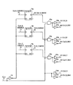
図1は、この発明にかかる低消費電力回路の設計方法の一実施の形態による低消費電力回路の設計方法を説明する図である。図1において、モジュールA1,モジュールB2,モジュールC3およびモジュールD4は、それぞれ論理回路の回路要素であるフリップフロップを、供給するクロック信号によってグループ化したモジュールであり、次のようにして分割され、クロックの供給が行われる。なお、少なくともモジュールA1,モジュールB2およびモジュールC3は、モジュール間のデータ転送に関わる信号数が少なくなるように分割されている。
Embodiment 1 FIG.
FIG. 1 is a diagram for explaining a low power consumption circuit design method according to an embodiment of a low power consumption circuit design method according to the present invention. In FIG. 1, a module A1, a module B2, a module C3, and a module D4 are modules in which flip-flops, which are circuit elements of a logic circuit, are grouped by supplied clock signals, and are divided as follows. Is supplied. At least the module A1, the module B2, and the module C3 are divided so that the number of signals related to data transfer between the modules is reduced.
すなわち、半導体集積回路の論理回路に存するフリップフロップを、まず、データを取り込むためのイネーブル条件付きのフリップフロップ(以降「データイネーブル条件付きのフリップフロップ」と記す)と、常にクロック信号が供給されそのクロック信号に同期してデータを常に取り込み続けるフリップフロップ(以降「フリーランクロック信号が供給されるフリップフロップ」と記す)とに分ける。 That is, a flip-flop existing in a logic circuit of a semiconductor integrated circuit is first supplied with a clock signal that is always supplied with a flip-flop with an enable condition for fetching data (hereinafter referred to as a “flip-flop with a data enable condition”). The data is divided into flip-flops (hereinafter referred to as “flip-flops to which a free-run clock signal is supplied”) that constantly captures data in synchronization with the clock signal.
次に、データイネーブル条件付きのフリップフロップを複数のモジュールに分割(図1ではモジュールA1,モジュールB2,モジュールC2の3つを示す)し、それぞれのモジュールにおけるフリップフロップの全てがデータを取り込むタイミングのみでクロックを供給するためのクロックイネーブル条件(クロックイネーブル条件信号CLK_A_ENABLE14,CLK_B_ENABLE15,CLK_C_ENABLE16)をそれぞれ生成する回路(クロックイネーブル条件生成回路5,6,7)を設計する。
Next, the flip-flop with the data enable condition is divided into a plurality of modules (three modules A1, B2, and C2 are shown in FIG. 1), and only the timing at which all the flip-flops in each module capture data. Are designed to generate clock enable conditions (clock enable condition signals CLK_A_ENABLE14, CLK_B_ENABLE15, CLK_C_ENABLE16) for supplying the clock at (clock enable
そして、それらのクロックイネーブル条件(クロックイネーブル条件信号CLK_A_ENABLE14,CLK_B_ENABLE15,CLK_C_ENABLE16)と基準クロック信号9とに基づき、データを取り込むタイミングのみでクロック供給となりその他のタイミングではクロック供給の停止となる供給・停止付きのクロック信号(クロック信号CLK_A10,CLK_B11,CLK_B12)を対応するモジュール(モジュールA1,モジュールB2,モジュールC2)に分配供給するクロック生成回路8を設計する。
Then, based on these clock enable conditions (clock enable condition signals CLK_A_ENABLE14, CLK_B_ENABLE15, CLK_C_ENABLE16) and the
また、フリーランクロック信号が供給されるフリップフロップも複数のモジュールに分割(図1ではモジュールD4の1個を示す)し、クロック生成回路8はフリーランクロック信号(クロック信号CLK_D13)を基準クロック信号9に基づき供給するように設計する。
Further, the flip-flop to which the free-run clock signal is supplied is also divided into a plurality of modules (one of the modules D4 is shown in FIG. 1), and the
次に、互いに異なるクロック信号が入力されるモジュール間のデータ転送部分に、データ送信側モジュールのクロック信号を反転したクロック信号で動作するフリップフロップを挿入する。すなわち、図1に示すように、クロック生成回路8に、クロック信号CLK_A10を反転するインバータ23aと、クロック信号CLK_B11を反転するインバータ23bと、クロック信号CLK_C12を反転するインバータ23cと、クロック信号CLK_D13を反転するインバータ23dとをそれぞれ設ける。
Next, a flip-flop that operates with a clock signal obtained by inverting the clock signal of the data transmitting module is inserted into a data transfer portion between modules to which different clock signals are input. That is, as shown in FIG. 1, the
そして、モジュールA1からモジュールB2へのデータ転送部分に、インバータ23aが出力する反転クロック信号CLK_A_INV40で駆動されるフリップフロップ20aを挿入する。モジュールB2からモジュールA1へのデータ転送部分とモジュールB2からモジュールC3へのデータ転送部分とに、インバータ23bが出力する反転クロック信号CLK_B_INV41で駆動されるフリップフロップ2b,2cをそれぞれ挿入する。同様にモジュールC3からモジュールB2へのデータ転送部分とモジュールC3からモジュールD4へのデータ転送部分とに、インバータ23cが出力する反転クロック信号CLK_C_INV42で駆動されるフリップフロップ2d,2eをそれぞれ挿入する。また、モジュールD4からモジュールC3へのデータ転送部分に、インバータ23dが出力する反転クロック信号CLK_D_INV43で駆動されるフリップフロップ2fに挿入する。
Then, the flip-
この設計方法によれば、モジュール間のデータ転送は、データ送信側のモジュールに供給するクロック信号を反転したクロック信号でデータを取り込むフリップフロップを介して行うようにしたので、クロックスキューの影響無しにモジュール間のデータ転送が行えるようになる。しかも、データイネーブル付きフリップフロップに関わるモジュール間のデータ転送に用いる反転したクロック信号は、データ転送に必要なタイミングのみでクロック信号が供給されるので、低消費電力化も実現することができる。このような低消費電力回路は、半導体デバイスの種類を問わずに設計することができる。また、クロックスキュー等のタイミングの問題が発生しないので、確実に動作する。 According to this design method, data transfer between modules is performed via a flip-flop that takes in data with a clock signal obtained by inverting the clock signal supplied to the module on the data transmission side, so that there is no influence of clock skew. Data can be transferred between modules. In addition, since the inverted clock signal used for data transfer between modules related to the flip-flop with data enable is supplied only at the timing necessary for data transfer, low power consumption can also be realized. Such a low power consumption circuit can be designed regardless of the type of semiconductor device. In addition, since a timing problem such as clock skew does not occur, it operates reliably.
次に、図2は、図1に示すクロック生成回路8の構成例を示す回路図である。図2において、フリップフロップ18a,18b,18cの各データ入力端Dには、各モジュールのクロックイネーブル条件信号CLK_A_ENABLE14,CLK_B_ENABLE15,CLK_C_ENABLE16が印加されている。また、フリップフロップ18a,18b,18cの各クロック入力端Gには、基準クロック信号CLK9をインバータ19にて反転して印加されている。これによって、フリップフロップ18a,18b,18cの各データ出力端Qには、クロックマスク信号CLK_A_MASK29,CLK_B_MASK30,CLK_C_MASK31がそれぞれ出力される。
Next, FIG. 2 is a circuit diagram showing a configuration example of the
AND回路22a,22b,22cでは、一方の入力端に基準クロック信号CLK9が共通に印加されている。AND回路22aでは、他方の入力端にクロックマスク信号CLK_A_MASK29が印加され、出力端にバッファ24aとインバータ23aとが並列に接続されている。バッファ24aからはモジュールA1に対するクロック信号CLK_A10が出力される。インバータ23aからはデータ転送用のフリップフロップ20aに対する反転クロック信号CLK_A_INV40が出力される。
In the AND
AND回路22bでは、他方の入力端にクロックマスク信号CLK_B_MASK30が印加され、出力端にバッファ24bとインバータ23bとが並列に接続されている。バッファ24bからはモジュールB2に対するクロック信号CLK_B11が出力される。インバータ23bからはデータ転送用のフリップフロップ20b,20cに対する反転クロック信号CLK_B_INV41が出力される。
In the AND
AND回路22cでは、他方の入力端にクロックマスク信号CLK_C_MASK31が印加され、出力端にバッファ24cとインバータ23cとが並列に接続されている。バッファ24cからはモジュールC3に対するクロック信号CLK_C12が出力される。インバータ23cからはデータ転送用のフリップフロップ20d,20eに対する反転クロック信号CLK_C_INV42が出力される。
In the AND
また、基準クロック信号CLK9が並列に入力されるバッファ24dとインバータ23dと設けられている。バッファ24dからはモジュールD4に対するフリーランクロック信号CLK_D13が出力される。インバータ23dからはデータ転送用のフリップフロップ20fに対する反転クロック信号CLK_D_INV43が出力される。
Further, a
なお、図2に示すように、各モジュールに対するクロックイネーブル条件信号CLK_A_ENABLE14,CLK_B_ENABLE15,CLK_C_ENABLE16を、それぞれ基準クロック信号CLK9の反転クロック信号によってフリップフロップ18a,18b,18cに一旦ラッチし、それと基準クロック信号CLK9とのANDを取るようにしたので、モジュール等にはグリッジが乗らないクロック信号が供給されることになる。
As shown in FIG. 2, the clock enable condition signals CLK_A_ENABLE14, CLK_B_ENABLE15, and CLK_C_ENABLE16 for each module are once latched in flip-
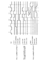
次に、図3〜図6を参照して、クロックスキューの影響無しにモジュール間のデータ転送を実現する方法を具体的に説明する。なお、図3は、クロック系統の異なるモジュール間のデータ転送において、クロックスキューの影響によってデータ転送が正しく行われない可能性のある回路例である。図4は、図3に示す回路においてモジュールA1からモジュールB2へのデータ転送動作を説明するタイムチャートである。図5は、図3に示す回路において、モジュールA1とモジュールB2との間のデータ転送部分に、転送元のクロック信号の反転クロック信号で駆動されるフリップフロップを挿入した回路例である。図6は、図5に示す回路においてモジュールA1からモジュールB2へのデータ転送動作を説明するタイムチャートである。 Next, a method for realizing data transfer between modules without the influence of clock skew will be specifically described with reference to FIGS. FIG. 3 is a circuit example in which data transfer may not be performed correctly due to the influence of clock skew in data transfer between modules of different clock systems. FIG. 4 is a time chart for explaining the data transfer operation from the module A1 to the module B2 in the circuit shown in FIG. FIG. 5 is a circuit example in which a flip-flop driven by an inverted clock signal of the transfer source clock signal is inserted in the data transfer portion between the module A1 and the module B2 in the circuit shown in FIG. FIG. 6 is a time chart for explaining the data transfer operation from the module A1 to the module B2 in the circuit shown in FIG.
図3では、説明を簡略化するために、2つのモジュールのモジュールA1とモジュールB2には、それぞれ、1個のフリップフロップ35,36が存在し、モジュールA1からモジュールB2に対して1本だけデータ転送経路がある場合の構成が示されている。モジュールA1からモジュールB3へのデータ転送は、複数のバッファを直列に接続したバッファ37を介して行われる。したがって、クロック生成回路8は、図2に示した構成とは異なり、モジュールA1へのクロック信号CLK_A10とモジュールB2へのクロック信号CLK_B11のみを生成する構成となる。
In FIG. 3, for simplification of explanation, two flip-
すなわち、図3において、モジュールA1では、2入力1出力のマルチプレクサ21aと1つのフリップフロップ35とが示されている。マルチプレクサ21aは、一方の入力端Aにフリップフロップ35のデータ出力端Qが接続され、他方の入力端に外部からデータ信号DATA_IN50が印加される。また、マルチプレクサ21aは、セット入力端Sに外部からデータイネーブル信号DATA_A_ENABLE52が印加され、出力端Yはフリップフロップ35のデータ入力端Dに接続されている。データイネーブル信号DATA_A_ENABLE52は、クロックイネーブル条件生成回路5にも入力されている。フリップフロップ35では、クロック入力端Gにクロック信号CLK_A10が印加される。そして、フリップフロップ35のデータ出力端Qに現れる出力データ信号DATA_OUT51は、マルチプレクサ21aの一方の入力端Aに印加されるとともに、バッファ37を介したモジュールB2への転送データとなる。
That is, in FIG. 3, the module A1 shows a 2-input 1-
モジュールB2では、2入力1出力のマルチプレクサ21bと1つのフリップフロップ36とが示されている。マルチプレクサ21bは、一方の入力端Aにフリップフロップ36のデータ出力端Qが接続され、他方の入力端にバッファ37からのデータ信号DATA_IN53が印加される。また、マルチプレクサ21bは、セット入力端Sに外部からデータイネーブル信号DATA_B_ENABLE55が印加され、出力端Yはフリップフロップ36のデータ入力端Dに接続されている。データイネーブル信号DATA_B_ENABLE55は、クロックイネーブル条件生成回路6にも入力されている。フリップフロップ36では、クロック入力端Gにクロック信号CLK_B11が印加される。そして、フリップフロップ35のデータ出力端Qに現れる出力データ信号DATA_OUT54は、マルチプレクサ21bの一方の入力端Aに印加される。
In the module B2, a two-input one-
ここで、モジュールA1に供給するクロック信号CLK_A10とモジュールB2に供給するクロック信号CLK_A11とには、図4に示すように、クロックスキュー60が存在する。図4では、基準クロックCLKのクロックサイクルT1,T2,T3,T4,T5における、モジュールA1内のフリップフロップ35の入出力関係(クロック信号CLK_A、データイネーブル信号DATA_A_ENABLE、入力データDATA_A_IN、出力データDATA_A_OUT)と、モジュールB2内のフリップフロップ36の入出力関係(クロック信号CLK_B、データイネーブル信号DATA_B_ENABLE、入力データDATA_B_IN、出力データDATA_B_OUT)とが示されている。
Here, the clock signal CLK_A10 supplied to the module A1 and the clock signal CLK_A11 supplied to the module B2 have a clock skew 60 as shown in FIG. In FIG. 4, the input / output relationship of the flip-
図4において、モジュールA1内のフリップフロップ35に供給するクロック信号CLK_Aは、クロックタイミングT1,T2とクロックタイミングT5以降では、低レベル(クロック供給停止)であり、クロックタイミングT3,T4での各前半サイクルにおいて高レベル(クロック供給)である。これに対し、モジュールB2内のフリップフロップ36に供給するクロック信号CLK_Bは、クロックの供給・停止の関係は、クロック信号CLK_Aと同じであるが、クロック信号CLK_Bの先頭供給クロックの位置は、クロックタイミングT4の前半サイクルの期間内においてクロックタイミングT4の開始時点からクロックスキュー60の分だけ位相が遅れた位置にシフトされている。
In FIG. 4, the clock signal CLK_A supplied to the flip-
モジュールA1内のフリップフロップ35では、データイネーブル信号DATA_A_ENABLEが、クロックタイミングT2,T3の期間内高レベルとなっている。入力データDATA_A_INは、クロックタイミングT2の終了時点まで高レベルであり、クロックタイミングT3の開始時点で低レベルとなり、以降それを維持している。出力データDATA_A_OUTは、クロック信号CLK_Aに応答して生成されるので、クロックタイミングT3の期間内では高レベルとなり、クロックタイミングT4の期間内では低レベルとなる。この出力データDATA_A_OUTが、バッファ37を介してモジュールB2に転送される。
In the flip-
モジュールB2内のフリップフロップ36では、データイネーブル信号DATA_B_ENABLEは、クロックスキュー60を考慮して生成されるので、クロックタイミングT3の開始時点からクロックスキュー60の分だけ遅れた位置にて高レベルとなり、クロックタイミングT5の開始時点からクロックスキュー60の分だけ遅れた位置にて低レベルとなっている。これに対し、入力データDATA_B_INは、モジュールA1が転送する出力データDATA_A_OUTであるので、クロックタイミングT3の期間内では高レベルとなり、クロックタイミングT4の期間内では低レベルとなる。
In the flip-
そうすると、この入力データDATA_B_INをサンプリングするクロック信号CLK_Bは、入力データDATA_B_INが低レベルを示すクロックタイミングT4の期間以降に存在するので、出力データDATA_B_OUTは、常に、低レベルのままとなる。 Then, since the clock signal CLK_B for sampling the input data DATA_B_IN exists after the period of the clock timing T4 in which the input data DATA_B_IN indicates a low level, the output data DATA_B_OUT always remains at a low level.
この問題を解決するために、図5に示すように、バッファ37に代えて、フリップフロップ20aを挿入する。そして、クロック生成回路8から、モジュールA1へのクロック信号CLK_A10の反転クロック信号CLK_A_INV40をフリップフロップ20aに供給する構成と採る。
In order to solve this problem, a flip-
このようにすると、図6に示すように、モジュールA1からモジュールB2への転送経路に挿入したフリップフロップ20aでは、反転クロック信号CLK_A_INV40がクロック信号CLK_Aの後半サイクルにシフトされた関係で入力するので、モジュールA1からの転送データである入力データDATA_T_INは、半サイクルだけシフトされてデータ出力端に現れるモジュールB2への出力データDATA_T_OUTとなる。
In this way, as shown in FIG. 6, in the flip-
その結果、モジュールB2内のフリップフロップ36では、フリップフロップ20aからの転送データである入力データDATA_A_INは、クロックタイミングT3の後半サイクルの開始時点からクロックタイミングT4の前半サイクルの終了時点までの期間内の高レベルとなる。クロック信号CLK_Bの先頭供給クロックの位置は、クロックタイミングT4の前半サイクルの期間内においてクロックタイミングT4の開始時点からクロックスキュー60の分だけ位相が遅れた位置に存するので、入力データDATA_A_INの高レベルをサンプリングすることができ、クロックタイミングT4の前半サイクルの途中からクロックタイミングT5の前半サイクルの途中まで高レベルで、クロックタイミングT5の前半サイクルの途中から図示してないがクロックタイミングT6の前半サイクルの途中まで低レベルとなるデータ出力DATA_B_OUTが得られる。
As a result, in the flip-
このように、モジュールA1の出力データDATA_A_OUTを、モジュールA1に供給するクロック信号CLK_A10の反転クロック信号CLK_A_INV40によって一旦、フリップフロップ20aにラッチし、モジュールB2に転送するようにすれば、モジュールA1とモジュールB2との間にクロックスキューがあっても、確実に、データを転送することができる。しかも、データ転送部分に追加したフリップフロップ20aには、データ転送時に必要なクロックのみしか供給されないので、消費電力を抑えることができる。
In this way, if the output data DATA_A_OUT of the module A1 is once latched in the flip-
実施の形態2.
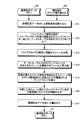
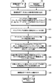
図7は、この発明にかかる低消費電力回路の設計支援装置の一実施の形態による低消費電力回路の設計支援装置の構成を示すフローチャートである。この実施の形態2では、実施の形態1に示したクロック系統の異なるモジュール間のデータ転送を実現する低消費電力回路の設計において、モジュール間のデータ転送数を考慮しないでモジュールの分割を行う設計支援装置の構成例が示されている。
FIG. 7 is a flowchart showing a configuration of a low power consumption circuit design support apparatus according to an embodiment of the low power consumption circuit design support apparatus according to the present invention. In the second embodiment, in the design of the low power consumption circuit that realizes the data transfer between the modules having different clock systems shown in the first embodiment, the module is divided without considering the number of data transfers between the modules. A configuration example of the support device is shown.
図7において、記憶装置100には、半導体集積回路の論理回路を、例えばHDL(Hardware Description Language)にて表現した論理記述データが格納されている。以降、記憶装置100に代えて、論理記述データ100と記す。また、記憶装置102には、当該設計対象の半導体集積回路に含まれるクロック信号の総数が含まれる制約条件が格納されている。以降、記憶装置102に代えて、制約条件102と記す。
In FIG. 7, the
当該低消費電力回路の設計支援装置を制御するコンピュータ上の支援プログラムでは、まず、論理記述データ100と制約条件102を読み込み(ステップS11)、論理回路に含まれるフリップフロップの種別の解析を行う(ステップS12)。つまり、ステップS12では、論理回路に含まれるフリップフロップが、フリーランクロック信号の供給されるフリップフロップであるか、或いは、データイネーブル付きのフリップフロップであるかの判別を行う。
In the support program on the computer that controls the design support device for the low power consumption circuit, first, the
そして、判別したフリップフロップの種別に従って、当該半導体集積回路をモジュールに分割する(ステップS13)。つまり、ステップS13では、フリーランクロック信号の供給されるフリップフロップをグループ化してモジュールに分割する。また、データイネーブル付きのフリップフロップをグループ化して別のモジュールに分割する。 Then, according to the determined type of flip-flop, the semiconductor integrated circuit is divided into modules (step S13). That is, in step S13, the flip-flops to which the free-run clock signal is supplied are grouped and divided into modules. Also, flip-flops with data enable are grouped and divided into different modules.
次いで、上記のように分割したデータイネーブル条件付きのフリップフロップが含まれるモジュールを、制約条件102として与えた半導体集積回路に含まれるクロック信号数を満足するように細かく分割する(ステップS14)。そして、系統の異なるクロック信号が供給されるモジュール間のデータ転送部分に、転送元のモジュールに供給するクロック信号を反転したクロック信号で駆動されるフリップフロップを挿入する(ステップS15)。 Next, the module including the flip-flop with the data enable condition divided as described above is finely divided so as to satisfy the number of clock signals included in the semiconductor integrated circuit given as the constraint condition 102 (step S14). Then, a flip-flop driven by a clock signal obtained by inverting the clock signal supplied to the transfer source module is inserted into the data transfer portion between the modules supplied with clock signals of different systems (step S15).
次いで、データイネーブル条件付きのフリップフロップが含まれる各モジュールについて、そのモジュール内のフリップフロップがデータを転送するタイミングのみでクロック信号が供給されるようにするクロックイネーブル条件を生成するクロックイネーブル条件生成回路と、前記各モジュールに対するクロックイネーブル条件によってデータを転送するタイミングのみでクロック供給となりその他のタイミングではクロック停止となる供給・停止付きのクロック信号および常にデータを取り込むフリップフロップに供給するフリーランクロック信号を生成するクロック生成回路とを生成する(ステップS16)。 Next, for each module including a flip-flop with a data enable condition, a clock enable condition generation circuit that generates a clock enable condition that allows a clock signal to be supplied only at the timing at which the flip-flop in the module transfers data And a clock signal with supply / stop that only supplies data at the timing of transferring data according to the clock enable condition for each module, and a free-run clock signal that is supplied to a flip-flop that always captures data at other timings. A clock generation circuit to be generated is generated (step S16).
そして、終了処理として、上述の手順にて処理して生成されたHDLなどによる論理記述データを記憶装置101に書き出す(ステップS17)。斯くして、記憶装置101には、この実施の形態2による低消費電力化技術適用後のHDL等で表現された論理記述データが格納される。
Then, as end processing, logical description data such as HDL generated by processing in the above-described procedure is written to the storage device 101 (step S17). Thus, the
以上の処理によって、異なるクロック信号が供給されるモジュール間転送においてクロックスキューによる誤動作の発生しない低消費電力化を実現した論理回路を支援プログラムにより生成することができる。 Through the above processing, a logic circuit realizing low power consumption that does not cause malfunction due to clock skew in inter-module transfer to which different clock signals are supplied can be generated by the support program.
実施の形態3.
図8は、この発明にかかる低消費電力回路の設計支援装置の他の実施の形態による低消費電力回路の設計支援装置の構成を説明するフローチャートである。この実施の形態3では、実施の形態1に示したクロック系統の異なるモジュール間のデータ転送を実現する低消費電力回路の設計において、モジュール間のデータ転送数を考慮してモジュールの分割を行う設計支援装置の構成例が示されている。
Embodiment 3 FIG.
FIG. 8 is a flowchart for explaining the configuration of a low power consumption circuit design support apparatus according to another embodiment of the low power consumption circuit design support apparatus according to the present invention. In the third embodiment, in the design of the low power consumption circuit that realizes the data transfer between the modules having different clock systems shown in the first embodiment, the module is divided in consideration of the number of data transfers between the modules. A configuration example of the support device is shown.
図8において、記憶装置100には、例えば、HDL(Hardware Description Language)にて論理回路を表現した論理記述データが格納されている。以降、記憶装置100に代えて、論理記述データ100と記す。また、記憶装置102には、出力する半導体集積回路に含まれるクロック信号の総数が含まれる制約条件が格納されている。以降、記憶装置102に代えて、制約条件102と記す。
In FIG. 8, the
当該低消費電力回路の設計支援装置を制御するコンピュータ上の支援プログラムでは、まず、論理記述データ100と制約条件102を読み込み(ステップS21)、論理回路に含まれるフリップフロップの種別の解析を行う(ステップS22)。つまり、ステップS22では、論理回路に含まれるフリップフロップが、フリーランクロック信号の供給されるフリップフロップであるか、或いは、データイネーブル付きのフリップフロップであるかの判別を行う。
In the support program on the computer that controls the design support apparatus for the low power consumption circuit, first, the
そして、判別したフリップフロップの種別に従って、当該半導体集積回路をモジュールに分割する(ステップS23)。つまり、ステップS23では、フリーランクロック信号の供給されるフリップフロップをグループ化してモジュールに分割する。また、データイネーブル付きのフリップフロップグをループ化して別のモジュールに分割する。 Then, according to the determined type of flip-flop, the semiconductor integrated circuit is divided into modules (step S23). That is, in step S23, the flip-flops to which the free-run clock signal is supplied are grouped and divided into modules. Also, the flip-flop with data enable is looped and divided into different modules.
次に、実施の形態2とは異なり、論理回路間、特に、データイネーブル条件付きのフリップフロップ間でのデータ転送経路を解析しその経路総数を調べる(ステップS24)。そして、モジュール分割後のモジュール間、特に、フリップフロップ間のデータ転送を行う信号線数が少なくなるように、ステップ23にて分割したデータイネーブル付きのフリップフロップグを含むモジュールを再分割する(ステップS25)。
Next, unlike the second embodiment, a data transfer path between logic circuits, particularly between flip-flops with data enable conditions, is analyzed and the total number of paths is examined (step S24). Then, the module including the flip-flop with data enable divided in
以降は実施の形態2と同様である。すなわち、系統の異なるクロック信号が供給されるモジュール間のデータ転送部分に、データ送信側モジュールに供給するクロック信号を反転したクロック信号で駆動されるフリップフロップを挿入する(ステップS26)。 The subsequent steps are the same as in the second embodiment. That is, a flip-flop driven by a clock signal obtained by inverting the clock signal supplied to the data transmission side module is inserted into a data transfer portion between modules to which clock signals of different systems are supplied (step S26).
次いで、データイネーブル条件付きのフリップフロップが含まれる各モジュールについて、そのモジュール内のフリップフロップがデータを転送するタイミングのみでクロック信号が供給されるようにするクロックイネーブル条件を生成するクロックイネーブル条件生成回路と、前記各モジュールに対するクロックイネーブル条件によってデータを転送するタイミングのみでクロック供給となりその他のタイミングではクロック停止となる供給・停止付きのクロック信号および常にデータを取り込むフリップフロップに供給するフリーランクロック信号を生成するクロック生成回路とを生成する(ステップS27)。 Next, for each module including a flip-flop with a data enable condition, a clock enable condition generation circuit that generates a clock enable condition that allows a clock signal to be supplied only at the timing at which the flip-flop in the module transfers data And a clock signal with supply / stop that only supplies data at the timing of transferring data according to the clock enable condition for each module, and a free-run clock signal that is supplied to a flip-flop that always captures data at other timings. A clock generation circuit to be generated is generated (step S27).
そして、終了処理として、上述の手順にて処理して生成されたHDLなどによる論理記述データを記憶装置101に書き出す(ステップS28)。斯くして、記憶装置101には、この実施の形態3による低消費電力化技術適用後のHDL等で表現された論理記述データが格納される。
Then, as end processing, logical description data such as HDL generated by processing in the above-described procedure is written to the storage device 101 (step S28). Thus, the
以上の処理によって、実施の形態2と同様に、異なるクロック信号が供給されるモジュール間転送においてクロックスキューによる誤動作の発生しない低消費電力化を実現した論理回路をプログラムにより生成することができる。加えて、モジュール間のデータ転送の数が少なくなるようにモジュール分割を行っているので、モジュール間に挿入されるフリップフロップの数が少なくなり、回路規模の増加を抑えることができるという効果が得られる。 Through the above processing, as in the second embodiment, a logic circuit that realizes low power consumption without causing malfunction due to clock skew in inter-module transfer to which different clock signals are supplied can be generated by a program. In addition, since the module is divided so that the number of data transfers between modules is reduced, the number of flip-flops inserted between the modules is reduced, and an increase in circuit scale can be suppressed. It is done.
以上説明したように、この発明によれば、クロックスキューの影響の無い低消費電力回路を半導体デバイスの種類に依存しないで設計することができる。これによって、半導体集積回路のレイアウトを行った後にクロックスキューの問題が発生し、タイミングが収束しなくなった最悪の場合に、今までは製造後に論理回路の誤動作が発生していたが、そのような問題を無くすことができる。 As described above, according to the present invention, it is possible to design a low power consumption circuit that is not affected by clock skew without depending on the type of semiconductor device. As a result, a clock skew problem occurs after the layout of the semiconductor integrated circuit is performed, and in the worst case where the timing does not converge, a logic circuit malfunction has occurred until now. The problem can be eliminated.
特に、FPGAのように、予めロジックセルに対してクロック配線が行われている半導体集積回路の場合には、チップ内で使用できるクロック信号が定められているので、この発明によれば、そのクロック信号数に合うような論理回路が作成することができるようになる。 In particular, in the case of a semiconductor integrated circuit in which clock wiring is performed in advance on a logic cell, such as an FPGA, a clock signal that can be used in a chip is determined. A logic circuit suitable for the number of signals can be created.
また、系統の異なるクロック間のクロックスキューを考慮しなくてよいのでレイアウト以降の工数を短縮できる。さらに、ためのイネーブル条件が付いているフリップフロップが含まれるモジュールでは、各モジュール内のフリップフロップがデータを取り込むために必要なタイミングのみにクロック信号を供給することができるようになるので、論理回路の電力消費の殆どを占めるスイッチングを削減することができ、低消費電力化を実現することができる。 In addition, since it is not necessary to consider clock skew between clocks of different systems, man-hours after layout can be shortened. Furthermore, in a module including flip-flops with an enable condition for, a clock signal can be supplied only at a timing necessary for the flip-flops in each module to capture data. Switching that occupies most of the power consumption can be reduced, and low power consumption can be realized.
以上のように、この発明にかかる低消費電力回路の設計方法は、半導体集積回路の論理回路の低消費電力回路化設計を、クロックスキューを考慮する必要が無く、かる半導体デバイスの種類に依存せずに実施するのに有用である。 As described above, the design method of the low power consumption circuit according to the present invention does not require the clock skew to be considered in the design of the logic circuit of the semiconductor integrated circuit, and depends on the type of the semiconductor device. It is useful to implement without.
また、この発明にかかる低消費電力回路の設計支援装置は、クロックスキューを考慮する必要が無く、かつ半導体デバイスの種類に関係なく低消費電力回路化した論理回路をコンピュータ上の支援プログラムにて自動生成するのに有用である。 The low power consumption circuit design support apparatus according to the present invention does not need to consider clock skew, and automatically generates a low power consumption circuit logic circuit by a support program on a computer regardless of the type of semiconductor device. Useful for generating.
1 モジュールA(論理回路の回路要素を供給するクロック信号でグループ化したモジュールで、データイネーブル付きのフリップフロップを含む)、
2 モジュールB(論理回路の回路要素を供給するクロック信号でグループ化したモジュールで、データイネーブル付きのフリップフロップを含む)、
3 モジュールC(論理回路の回路要素を供給するクロック信号でグループ化したモジュール、データイネーブル付きのフリップフロップを含む)、
4 モジュールD(論理回路の回路要素を供給するクロック信号でグループ化したモジュールで、フリーランクロック信号によって駆動されるフリップフロップを含む)、
5 モジュールAのクロックイネーブル条件生成回路、
6 モジュールBのロックイネーブル条件生成回路、
7 モジュールCのクロックイネーブル条件生成回路、
8 クロック生成回路、
18a,18b,18c フリップフロップ、
20a,20b,20c,20d,20e,20f フリップフロップ、
21a,21b 2入力1出力のマルチプレクサ、
22a,22b,22c AND回路、
23a,23b,23c,23d インバータ、
24a,24b,24c,24d,37 バッファ、
35,36 フリップフロップ、
60 クロックスキュー、
100,101,102 記憶装置。
1 Module A (module grouped by clock signals that supply circuit elements of the logic circuit, including flip-flops with data enable),
2 Module B (module grouped by clock signals that supply circuit elements of the logic circuit, including flip-flops with data enable),
3 Module C (including modules grouped by clock signals that supply circuit elements of the logic circuit, including flip-flops with data enable),
4 Module D (modules grouped with clock signals that supply circuit elements of the logic circuit, including flip-flops driven by free-run clock signals),
5 Clock enable condition generation circuit for module A,
6 Module B lock enable condition generation circuit,
7 Clock enable condition generation circuit for module C,
8 Clock generation circuit,
18a, 18b, 18c flip-flops,
20a, 20b, 20c, 20d, 20e, 20f flip-flop,
21a, 21b 2-input 1-output multiplexer,
22a, 22b, 22c AND circuit,
23a, 23b, 23c, 23d inverter,
24a, 24b, 24c, 24d, 37 buffers,
35, 36 flip-flops,
60 clock skew,
100, 101, 102 Storage device.
Claims (4)
前記第1フリップフロップのグループを複数の第1モジュールに分割し、前記第2フリップフロップのグループを1以上の第2モジュールに分割する工程と、
分割したモジュールを単位として、前記第1モジュールでは、そのモジュールに含まれる第1フリップフロップに対し、前記イネーブル条件に従ってデータを取り込むタイミングではクロック供給となりその他のタイミングではクロック停止となる供給・停止付きのクロック信号が供給されるようにし、前記第2モジュールでは、そのモジュールに含まれる第2フリップフロップに対し、常にクロック供給となりデータの取り込みを連続して行わせるクロック信号が供給されるようにする工程と、
前記分割したモジュール間のデータ転送経路に、データ送信側のモジュールに供給する前記クロック信号を反転したクロック信号でデータを取り込むフリップフロップを挿入する工程と、
を含むことを特徴とする低消費電力回路の設計方法。 A step of dividing flip-flops in a logic circuit of a semiconductor integrated circuit into a first flip-flop group having an enable condition for capturing data and a second flip-flop group having no enable condition for capturing the data When,
Dividing the first flip-flop group into a plurality of first modules, and dividing the second flip-flop group into one or more second modules;
With the divided module as a unit, the first module includes a supply / stop function that supplies the clock to the first flip-flop included in the module at the timing of capturing data according to the enable condition and stops the clock at other timings. A step of supplying a clock signal, and the second module is configured to supply a clock signal that is always supplied to the second flip-flop included in the module and continuously takes in data. When,
Inserting a flip-flop that captures data with a clock signal obtained by inverting the clock signal supplied to the data transmission side module in the data transfer path between the divided modules;
A method for designing a low power consumption circuit, comprising:
前記判別手段の判別結果に基づき、イネーブル条件付きのフリップフロップをグループ化してモジュールに分割し、イネーブル条件付きでないフリップフロップをグループ化して別のモジュールに分割する手段と、
前記制約条件として与えた半導体集積回路に含まれるクロック信号数を満足するように前記分割したイネーブル条件付きのフリップフロップが含まれるモジュールを細かく分割する手段と、
系統の異なるクロック信号が供給されるモジュール間のデータ転送経路に、送信側のモジュールに供給するクロック信号を反転したクロック信号で駆動されるフリップフロップを挿入する手段と、
前記イネーブル条件付きのフリップフロップが含まれる各モジュールについてそのモジュール内のフリップフロップがデータを取り込むタイミングのみでクロック信号が供給されるようにするクロックイネーブル条件を生成する回路を生成する手段と、
前記イネーブル条件付きのフリップフロップが含まれる各モジュールに対しては各モジュールに対する前記クロックイネーブル条件に基づき、そのモジュール内のフリップフロップがデータを取り込むタイミングではクロック供給となりその他のタイミングではクロック供給停止となる供給・停止付きのクロック信号を生成する一方、前記イネーブル条件付きでないフリップフロップが含まれる各モジュールに対してはそのモジュール内のフリップフロップがデータの取り込みを連続して行うように常にクロック供給となるクロック信号を供給する回路を生成する手段と、
前記の各手段によって生成された論理記述データを設計結果として出力する手段と、
を備えたことを特徴とする低消費電力回路の設計支援装置。 An enable for a flip-flop connected to the clock signal to capture data based on logic description data representing a logic circuit of the semiconductor integrated circuit and a constraint condition including the total number of clock signals included in the semiconductor integrated circuit Means for determining whether it is conditional;
Based on the determination result of the determination means, the flip-flops with enable conditions are grouped and divided into modules, and the flip-flops without enable conditions are grouped and divided into different modules;
Means for finely dividing a module including the divided flip-flops with enable conditions so as to satisfy the number of clock signals included in the semiconductor integrated circuit given as the constraint condition;
Means for inserting a flip-flop driven by a clock signal obtained by inverting the clock signal supplied to the module on the transmission side in a data transfer path between modules to which clock signals of different systems are supplied;
Means for generating a circuit for generating a clock enable condition for each module including the flip-flop with the enable condition so that a clock signal is supplied only at a timing when the flip-flop in the module fetches data; and
For each module including the flip-flop with the enable condition, based on the clock enable condition for each module, the clock supply is performed at the timing when the flip-flop in the module captures data, and the clock supply is stopped at other timings. While generating a clock signal with supply / stop, for each module including a flip-flop without the enable condition, the clock is always supplied so that the flip-flop in the module continuously fetches data. Means for generating a circuit for supplying a clock signal;
Means for outputting the logical description data generated by each means as a design result;
A design support apparatus for a low power consumption circuit, comprising:
前記判別手段の判別結果に基づき、イネーブル条件付きのフリップフロップをグループ化してモジュールに分割し、イネーブル条件付きでないフリップフロップをグループ化して別のモジュールに分割する手段と、
少なくとも、前記イネーブル条件付きのフリップフロップ間でのデータ転送経路を解析し、その経路総数を調べる手段と、
前記経路総数に基づき、モジュール分割後のモジュール間でのデータ転送を行う信号数が少なくなるように、前記分割したイネーブル条件付きのフリップフロップが含まれるモジュールを再分割する手段と、
系統の異なるクロック信号が供給されるモジュール間のデータ転送経路に、送信側のモジュールに供給するクロック信号を反転したクロック信号で駆動されるフリップフロップを挿入する手段と、
前記イネーブル条件付きのフリップフロップが含まれる各モジュールについてそのモジュール内のフリップフロップがデータを取り込むタイミングのみでクロック信号が供給されるようにするクロックイネーブル条件を生成する回路を生成する手段と、
前記イネーブル条件付きのフリップフロップが含まれる各モジュールに対しては各モジュールに対する前記クロックイネーブル条件に基づき、そのモジュール内のフリップフロップがデータを取り込むタイミングではクロック供給となりその他のタイミングではクロック供給停止となる供給・停止付きのクロック信号を生成する一方、前記イネーブル条件付きでないフリップフロップが含まれる各モジュールに対してはそのモジュール内のフリップフロップがデータの取り込みを連続して行うように常にクロック供給となるクロック信号を供給する回路を生成する手段と、
前記の各手段によって生成された論理記述データを設計結果として出力する手段と、
を備えたことを特徴とする低消費電力回路の設計支援装置。
An enable for a flip-flop connected to the clock signal to capture data based on logic description data representing a logic circuit of the semiconductor integrated circuit and a constraint condition including the total number of clock signals included in the semiconductor integrated circuit Means for determining whether it is conditional;
Based on the determination result of the determination means, the flip-flops with enable conditions are grouped and divided into modules, and the flip-flops without enable conditions are grouped and divided into different modules;
Means for analyzing at least a data transfer path between flip-flops with the enable condition and checking the total number of paths;
Means for re-dividing the module including the divided flip-flops with enable conditions so that the number of signals for performing data transfer between modules after module division is reduced based on the total number of paths;
Means for inserting a flip-flop driven by a clock signal obtained by inverting the clock signal supplied to the module on the transmission side in a data transfer path between modules to which clock signals of different systems are supplied;
Means for generating a circuit for generating a clock enable condition for each module including the flip-flop with the enable condition so that a clock signal is supplied only at a timing when the flip-flop in the module fetches data; and
For each module including the flip-flop with the enable condition, based on the clock enable condition for each module, the clock supply is performed at the timing when the flip-flop in the module captures data, and the clock supply is stopped at other timings. While generating a clock signal with supply / stop, for each module including a flip-flop without the enable condition, the clock is always supplied so that the flip-flop in the module continuously fetches data. Means for generating a circuit for supplying a clock signal;
Means for outputting the logical description data generated by each means as a design result;
A design support apparatus for a low power consumption circuit, comprising:
Priority Applications (1)
| Application Number | Priority Date | Filing Date | Title |
|---|---|---|---|
| JP2004109259A JP4319081B2 (en) | 2004-04-01 | 2004-04-01 | Low power circuit design support device |
Applications Claiming Priority (1)
| Application Number | Priority Date | Filing Date | Title |
|---|---|---|---|
| JP2004109259A JP4319081B2 (en) | 2004-04-01 | 2004-04-01 | Low power circuit design support device |
Publications (2)
| Publication Number | Publication Date |
|---|---|
| JP2005293372A true JP2005293372A (en) | 2005-10-20 |
| JP4319081B2 JP4319081B2 (en) | 2009-08-26 |
Family
ID=35326210
Family Applications (1)
| Application Number | Title | Priority Date | Filing Date |
|---|---|---|---|
| JP2004109259A Expired - Fee Related JP4319081B2 (en) | 2004-04-01 | 2004-04-01 | Low power circuit design support device |
Country Status (1)
| Country | Link |
|---|---|
| JP (1) | JP4319081B2 (en) |
Cited By (1)
| Publication number | Priority date | Publication date | Assignee | Title |
|---|---|---|---|---|
| CN114970415A (en) * | 2022-04-14 | 2022-08-30 | Oppo广东移动通信有限公司 | Circuit generation method and device, storage medium and electronic equipment |
-
2004
- 2004-04-01 JP JP2004109259A patent/JP4319081B2/en not_active Expired - Fee Related
Cited By (1)
| Publication number | Priority date | Publication date | Assignee | Title |
|---|---|---|---|---|
| CN114970415A (en) * | 2022-04-14 | 2022-08-30 | Oppo广东移动通信有限公司 | Circuit generation method and device, storage medium and electronic equipment |
Also Published As
| Publication number | Publication date |
|---|---|
| JP4319081B2 (en) | 2009-08-26 |
Similar Documents
| Publication | Publication Date | Title |
|---|---|---|
| Thonnart et al. | A fully-asynchronous low-power framework for GALS NoC integration | |
| Muttersbach et al. | Practical design of globally-asynchronous locally-synchronous systems | |
| US8286025B1 (en) | Selection of port adapters for clock crossing boundaries | |
| US9098666B2 (en) | Clock distribution network for 3D integrated circuit | |
| Kasapaki et al. | Argo: A time-elastic time-division-multiplexed noc using asynchronous routers | |
| Vitullo et al. | Low-complexity link microarchitecture for mesochronous communication in networks-on-chip | |
| US8578074B2 (en) | First in first out device and method thereof | |
| US20090271747A1 (en) | Logic circuit designing device, logic circuit designing method and logic circuit designing program for asynchronous logic circuit | |
| US8225259B1 (en) | Apparatus and methods for time-multiplex field-programmable gate arrays with multiple clocks | |
| Ax et al. | Comparing synchronous, mesochronous and asynchronous NoCs for GALS based MPSoCs | |
| US6711089B2 (en) | Method and apparatus for performing signal synchronization | |
| US20020029361A1 (en) | Logic circuit design method and logic circuit | |
| JP2002524790A (en) | Synchronous polyphase clock distribution system | |
| Takizawa et al. | A design support tool set for asynchronous circuits with bundled-data implementation on FPGAs | |
| JP4319081B2 (en) | Low power circuit design support device | |
| JP2007027841A (en) | Design apparatus, method, and program for semiconductor integrated circuit | |
| Ludovici et al. | Comparing tightly and loosely coupled mesochronous synchronizers in a NoC switch architecture | |
| JPH10133768A (en) | Clock system, semiconductor device, semiconductor device test method, and CAD device | |
| Pilato et al. | A runtime adaptive controller for supporting hardware components with variable latency | |
| WO2024066950A1 (en) | Signal processing method, signal processing apparatus, chip, and electronic device | |
| US7676685B2 (en) | Method for improving the data transfer in semi synchronous clock domains integrated circuits at any possible m/n clock ratio | |
| Nag et al. | An autonomous clock gating technique in finite state machines based on registers partitioning | |
| KR100734521B1 (en) | IP Module for System-on-Chip | |
| Agiwal et al. | An architecture and a wrapper synthesis approach for multi-clock latency-insensitive systems | |
| JP2004326222A (en) | Data processing system |
Legal Events
| Date | Code | Title | Description |
|---|---|---|---|
| A621 | Written request for application examination |
Free format text: JAPANESE INTERMEDIATE CODE: A621 Effective date: 20061215 |
|
| A977 | Report on retrieval |
Free format text: JAPANESE INTERMEDIATE CODE: A971007 Effective date: 20090223 |
|
| A131 | Notification of reasons for refusal |
Free format text: JAPANESE INTERMEDIATE CODE: A131 Effective date: 20090303 |
|
| A521 | Written amendment |
Free format text: JAPANESE INTERMEDIATE CODE: A523 Effective date: 20090428 |
|
| TRDD | Decision of grant or rejection written | ||
| A01 | Written decision to grant a patent or to grant a registration (utility model) |
Free format text: JAPANESE INTERMEDIATE CODE: A01 Effective date: 20090526 |
|
| A01 | Written decision to grant a patent or to grant a registration (utility model) |
Free format text: JAPANESE INTERMEDIATE CODE: A01 |
|
| A61 | First payment of annual fees (during grant procedure) |
Free format text: JAPANESE INTERMEDIATE CODE: A61 Effective date: 20090527 |
|
| FPAY | Renewal fee payment (event date is renewal date of database) |
Free format text: PAYMENT UNTIL: 20120605 Year of fee payment: 3 |
|
| R150 | Certificate of patent or registration of utility model |
Free format text: JAPANESE INTERMEDIATE CODE: R150 |
|
| FPAY | Renewal fee payment (event date is renewal date of database) |
Free format text: PAYMENT UNTIL: 20130605 Year of fee payment: 4 |
|
| R250 | Receipt of annual fees |
Free format text: JAPANESE INTERMEDIATE CODE: R250 |
|
| R250 | Receipt of annual fees |
Free format text: JAPANESE INTERMEDIATE CODE: R250 |
|
| LAPS | Cancellation because of no payment of annual fees |