JP2005293333A - Real-time control system - Google Patents
Real-time control system Download PDFInfo
- Publication number
- JP2005293333A JP2005293333A JP2004108735A JP2004108735A JP2005293333A JP 2005293333 A JP2005293333 A JP 2005293333A JP 2004108735 A JP2004108735 A JP 2004108735A JP 2004108735 A JP2004108735 A JP 2004108735A JP 2005293333 A JP2005293333 A JP 2005293333A
- Authority
- JP
- Japan
- Prior art keywords
- real
- host computer
- control system
- device controller
- time control
- Prior art date
- Legal status (The legal status is an assumption and is not a legal conclusion. Google has not performed a legal analysis and makes no representation as to the accuracy of the status listed.)
- Granted
Links
Images


Landscapes
- Programmable Controllers (AREA)
- Testing And Monitoring For Control Systems (AREA)
Abstract
システム全体としてリソースを有効活用し、開発から生産終了までの製品コストを削減できるリアルタイム制御システムを提供することにある。
【課題】
【解決手段】
ホストコンピュータ10と、フィールドデバイスDSの制御を行う複数のデバイスコントローラが接続され、フィールドデバイスDSをリアルタイムで制御する。ホストコンピュータ10は、デバイスコントローラ100への制御内容を、一定時間で処理可能なファンクションに分割して転送し、デバイスコントローラ100は、ホストコンピュータ10から転送されたファンクションに基づいて、フィールドデバイスDSをリアルタイムで制御する。デバイスコントローラ100は、それぞれ、共通な部品で構成される標準部110と、接続されるフィールドデバイスによって異なる構成を持つ拡張部150とから分割して構成され、標準部110と拡張部150とは、コネクタC10,C20を介してバス接続される。
【選択図】 図1
The object is to provide a real-time control system that can effectively use resources as a whole system and reduce the product cost from development to end of production.
【Task】
[Solution]
The host computer 10 and a plurality of device controllers that control the field device DS are connected to control the field device DS in real time. The host computer 10 divides and transfers the control contents to the device controller 100 into functions that can be processed in a fixed time, and the device controller 100 transfers the field device DS in real time based on the functions transferred from the host computer 10. To control. The device controller 100 is configured by being divided from a standard unit 110 configured by common parts and an expansion unit 150 having a different configuration depending on a connected field device. The standard unit 110 and the expansion unit 150 are respectively Bus connections are made via connectors C10 and C20.
[Selection] Figure 1
Description
本発明は、ホストコンピュータにより、複数のフィールドデバイスの制御を行う複数のデバイスコントローラをリアルタイムで制御するリアルタイム制御システムに係り、特に、部品改廃や装置構成の変更などにより、制御コントローラや、I/Oなどのデバイスを、頻繁に変更する必要のあるシステムに用いるに好適なリアルタイム制御システムに関する。 The present invention relates to a real-time control system that controls a plurality of device controllers that control a plurality of field devices in real time by a host computer. In particular, the present invention relates to a control controller, an I / O, etc. The present invention relates to a real-time control system suitable for use in a system that needs to be frequently changed.
医療の分野で使われている自動分析装置や、成分分析や質量分析などの理化学機器などの装置においては、ユーザインタフェイスとなるパーソナルコンピュータ(ホストコンピュータ)と、フィールドデバイスの制御を行う制御コントローラとI/Oを制御するI/Oボードとからなるデバイスコントローラとによって、制御システムを構成する方法がよく用いられている。これは、パーソナルコンピュータでコマンドの発行や測定データの表示を行い、制御コントローラによりユーザの入力したコマンドを解してリアルタイム制御を行い、I/Oボードによりモータ,バルブ,センサなどのフィールドデバイスを制御するものである。 In automated analyzers used in the medical field, and physics and chemistry instruments such as component analysis and mass spectrometry, a personal computer (host computer) serving as a user interface, a controller for controlling field devices, A method of configuring a control system with a device controller including an I / O board that controls I / O is often used. This is done by issuing commands and displaying measurement data on a personal computer, using the controller to solve commands entered by the user, performing real-time control, and controlling field devices such as motors, valves, and sensors using the I / O board. To do.
ここで、制御コントローラとI/Oボードは同一のラックに格納され、バスによって互いにデータのやり取りができるよう接続されている。このバスとしては、たとえばVME(IEEE1014標準の非同期バス)やコンパクトPCIバスなどが用いられ、ラック内に基板が複数挿入できるように配置された接続スロットを介して、制御コントローラと複数のI/Oボードをバス接続する形態の制御システムが広く用いられている。 Here, the controller and the I / O board are stored in the same rack, and are connected so as to exchange data with each other via a bus. As this bus, for example, a VME (IEEE 1014 standard asynchronous bus) or a compact PCI bus is used, and a control controller and a plurality of I / Os are connected via a connection slot arranged so that a plurality of boards can be inserted into the rack. Control systems in which boards are connected by bus are widely used.
このような制御システムは、例えば、特開2003−229760号公報等に、大規模装置に適用した場合のシステム概略が記載されている。 Such a control system is described in, for example, Japanese Patent Application Laid-Open No. 2003-229760, and a system outline when applied to a large-scale apparatus.
装置の制御においては、モータ,バルブ,センサといったフィールドデバイスをシステム設計時に作成したタイムチャートに従って手順どおりに動作させていく必要がある。これは、デバイスを動作する順序が異なってしまったり、必要な時間までにデバイスを動作できなければ、機構系が期待通りの動作をとらなかったり、測定性能が未達となる。よって、制御システムにおいては、上述のタイムチャートを実現できるよう、ある決まった最小時間間隔ごとに処理を実行するリアルタイム性が要求される。 In the control of the apparatus, it is necessary to operate field devices such as motors, valves, and sensors according to procedures according to a time chart created at the time of system design. This is because if the order in which the devices are operated differs, or if the devices cannot be operated by a required time, the mechanism system does not operate as expected or the measurement performance is not achieved. Therefore, the control system is required to have a real-time property of executing processing at a certain minimum time interval so that the above-described time chart can be realized.
近年、パーソナルコンピュータの高速化/低価格化は年々劇的に進行しており、以前に比べて高速なCPU,容量の大きいメモリやハードディスクを搭載したモデルが安価に入手することができる。また、OSについても、RT−Linuxなど、以前はパーソナルコンピュータでは不得手とされてきたリアルタイム性に特化したものが開発されてきている。同様に制御に用いるマイクロプロセッサにおいても動作クロックの高速化が顕著に進行している。また、PCMCIAやCFカードなど、記憶媒体とのインタフェイスやUSB/LANといった通信インタフェイスなどの付帯機能が充実してきている。 In recent years, the speeding up / cost reduction of personal computers has progressed dramatically year by year, and a model equipped with a faster CPU, a larger capacity memory and a hard disk can be obtained at lower cost than before. As for the OS, RT-Linux and the like have been developed that specialize in real-time characteristics that have been previously unsatisfactory with personal computers. Similarly, in the microprocessor used for control, the operation clock speed is remarkably increased. Also, incidental functions such as an interface with a storage medium such as a PCMCIA and a CF card and a communication interface such as a USB / LAN have been enhanced.
一方、装置においては競合製品との競争力を強化するためにも、製品出荷までの開発費,生産コスト,メインテナンスやバージョンアップなどの出荷後のサポート費の削減が強く望まれている。これに対して従来技術によるリアルタイム制御システムのアーキテクチャを今後とも踏襲し続けてゆくとすると、以下の3点の問題が発生する。 On the other hand, in order to strengthen the competitiveness of competing products, there is a strong demand for reducing post-shipment support costs such as development costs, production costs, maintenance and version upgrades before product shipment. On the other hand, if the architecture of the real-time control system according to the prior art is continued, the following three problems will occur.
第1は、マイクロプロセッサの付帯機能の充実化によりデバイスコントローラに機能が集中し、上位のパーソナルコンピュータにおいてはある程度までのリアルタイム性を許容するにもかかわらず、あまり使用されず機能分担のバランスの悪いシステムとなってしまうことである。すなわち、デバイスコントローラとパーソナルコンピュータにおいてリソースが重複するため、コスト高となる。 First, functions are concentrated on the device controller due to the enhancement of the auxiliary functions of the microprocessor, and although the real-time property is allowed to some extent in the upper personal computer, it is not used so much and the balance of function sharing is poor. It becomes a system. That is, since resources overlap between the device controller and the personal computer, the cost increases.
第2は、デバイスコントローラにおいては制御プログラムはオンボードのフラッシュメモリなどを利用し格納するのが一般的である。これに対してパーソナルコンピュータにおいても、ハードディスクやメモリカード、光学式ドライブなどを不揮発性のデータ保存手段をもっている。すなわちここにおいてもリソースの重複が発生している。また、フラッシュメモリの書き込みにおいては、書き込み用のパーソナルコンピュータから書きこみデータをダウンロードしてフラッシュメモリに書き込みを行う方法や、ロムライターを使用して書き込み用のパソコンからフラッシュメモリに書き込みを行う方法などが一般的である。このような書きこみ作業は非効率的であり、分散制御システムなど複数のデバイスコントローラを用いる場合は多数の不揮発性メモリに書き込みを行わなくてはならないため、特に、生産コスト高となる。 Second, in a device controller, the control program is generally stored using an on-board flash memory or the like. On the other hand, a personal computer also has a nonvolatile data storage means such as a hard disk, a memory card, and an optical drive. In other words, resource duplication also occurs here. Also, in writing to flash memory, you can download data from a personal computer for writing and write to flash memory, or write to flash memory from a personal computer for writing using a ROM writer, etc. Is common. Such a writing operation is inefficient, and when a plurality of device controllers such as a distributed control system are used, a large number of nonvolatile memories must be written.
第3は、部品改廃の問題である。デバイスコントローラに使用される電子部品のうち、特にメモリは改廃のサイクルが短い。この理由は、揮発性メモリ/不揮発性メモリともにアプリケーションやユーザの要求する容量は年々増加の一途をたどっており、半導体メーカとしてもこの需要に応えるために日々、メモリの高速化大容量化に注力しているためである。一方、I/Oボードは改廃のサイクルが長いものである。デバイスコントローラとしては、この改廃の影響をできるだけ小さくしなくては、開発から生産終了までの製品ライフサイクルにおけるコスト増大となる。 Third, there is a problem of parts revision and abolition. Of the electronic components used in the device controller, especially the memory has a short cycle of reform. This is because the capacity required by applications and users for both volatile and non-volatile memories is steadily increasing year by year, and semiconductor manufacturers are focusing on increasing the memory speed and capacity every day to meet this demand. It is because it is doing. On the other hand, the I / O board has a long cycle of reform. As a device controller, unless the influence of the reform and reduction is made as small as possible, the cost in the product life cycle from development to end of production increases.
本発明の目的は、システム全体としてリソースを有効活用し、開発から生産終了までの製品コストを削減できるリアルタイム制御システムを提供することにある。 An object of the present invention is to provide a real-time control system capable of effectively using resources as a whole system and reducing the product cost from development to the end of production.
(1)上記目的を達成するために、本発明は、ホストコンピュータと、このホストコンピュータに接続され、フィールドデバイスの制御を行う複数のデバイスコントローラとからなり、前記フィールドデバイスをリアルタイムで制御するリアルタイム制御システムにおいて、前記ホストコンピュータは、前記デバイスコントローラへの制御内容を、一定時間で処理可能なファンクションに分割して転送し、前記デバイスコントローラは、前記ホストコンピュータから転送されたファンクションに基づいて、前記フィールドデバイスをリアルタイムで制御するようにしたものである。
かかる構成により、システム全体としてリソースを有効活用し、開発から生産終了までの製品コストを削減し得るものとなる。
(1) To achieve the above object, the present invention comprises a host computer and a plurality of device controllers connected to the host computer and controlling field devices, and controls the field devices in real time. In the system, the host computer divides and transfers the control contents to the device controller into functions that can be processed in a fixed time, and the device controller transfers the field based on the function transferred from the host computer. The device is controlled in real time.
With this configuration, it is possible to effectively use resources as a whole system and reduce product costs from development to the end of production.
(2)上記(1)において、好ましくは、前記デバイスコントローラは、それぞれ、共通な部品で構成される標準部と、接続されるフィールドデバイスによって異なる構成を持つ拡張部とから分割して構成され、前記標準部と前記拡張部とは、コネクタを介してバス接続されるものである。 (2) In the above (1), preferably, each of the device controllers is configured by being divided from a standard part constituted by common parts and an extension part having a different configuration depending on a connected field device, The standard part and the extension part are connected by a bus via a connector.
(3)上記(2)において、好ましくは、前記デバイスコントローラは、前記拡張部で保持している識別子を読み出し、前記ホストコンピュータに伝送し、前記ホストコンピュータは、前記デバイスコントローラから転送された識別子に基づいて、複数の前記デバイスコントローラを識別するようにしたものである。 (3) In the above (2), preferably, the device controller reads an identifier held in the extension unit and transmits the identifier to the host computer, and the host computer uses the identifier transferred from the device controller. Based on this, a plurality of the device controllers are identified.
(4)上記(1)において、好ましくは、前記デバイスコントローラは、前記ホストコンピュータから転送されたファンクションを格納する揮発性メモリを備えるようにしたものである。 (4) In the above (1), preferably, the device controller is provided with a volatile memory for storing a function transferred from the host computer.
(5)上記(1)において、好ましくは、前記ホストコンピュータは、前記デバイスコントローラに対し、前記ファンクションを一定周期で送付するようにしたものである。 (5) In the above (1), preferably, the host computer sends the function to the device controller at a constant cycle.
(6)上記(5)において、好ましくは、前記ホストコンピュータは、USB(Universal Serial Bus)を用いて、前記デバイスコントローラに前記ファンクションを転送するようにしたものである。 (6) In the above (5), preferably, the host computer transfers the function to the device controller using a USB (Universal Serial Bus).
(7)上記(1)において、好ましくは、前記デバイスコントローラは、前記ファンクションを実行した結果を、返値として前記ホストコンピュータに送信するようにしたものである。 (7) In the above (1), preferably, the device controller transmits a result of executing the function as a return value to the host computer.
(8)上記(1)において、好ましくは、前記ホストコンピュータ及び複数の前記デバイスコントローラは、ツリー型にネットワークにより接続されたものである。 (8) In the above (1), preferably, the host computer and the plurality of device controllers are connected in a tree shape by a network.
本発明によれば、システム全体としてリソースを有効活用し、開発から生産終了までの製品コストを削減できる。 According to the present invention, it is possible to effectively utilize resources as a whole system and reduce product costs from development to the end of production.
以下、図1〜図9を用いて、本発明の一実施形態によるリアルタイム制御システムの構成について説明する。
最初に、図1を用いて、本実施形態によるリアルタイム制御システムを適用した理化学装置の全体構成について説明する。
図1は、本発明の一実施形態によるリアルタイム制御システムを適用した理化学装置の全体構成を示す概略斜視図である。
Hereinafter, the configuration of a real-time control system according to an embodiment of the present invention will be described with reference to FIGS.
First, the overall configuration of the physics and chemistry apparatus to which the real-time control system according to the present embodiment is applied will be described with reference to FIG.
FIG. 1 is a schematic perspective view showing the entire configuration of a physics and chemistry apparatus to which a real-time control system according to an embodiment of the present invention is applied.
理化学装置とは、医療の分野で使われている自動分析装置や、成分分析や質量分析などの理化学機器などの装置である。装置内には多数のI/Oを有し、計測,分析などの処理を行うための搬送制御や、センサやアクチュエータの制御が行われている。 The physics and chemistry apparatus is an apparatus such as an automatic analyzer used in the medical field or a physics and chemistry instrument such as component analysis or mass spectrometry. The apparatus has a large number of I / Os, and transport control for performing processing such as measurement and analysis, and control of sensors and actuators are performed.
ホストコンピュータ10は、例えば、パーソナルコンピュータを使用している。理化学装置の操作者は、装置20A,20Bに対する計測,分析などの処理開始を指示する。理化学装置が、例えば、高速液体クロマトグラフ装置の場合、装置400Aはポンプやオートサンプラーであり、装置400Bはカラムオーブンや検出器である。なお、ポンプ,オートサンプラー,カラムオーブン,検出器を、それぞれ独立した装置として構成することもできる。
As the
ホストコンピュータ10と装置20A,20Bは、USB伝送線30Cによって接続されている。装置20A,20B側のインタフェイスとしては、USBハブ30Hを用いている。USB伝送線30Cは、USBハブ30Hによって分配され、ホストコンピュータ10は、装置20A,20Bのデバイスコントローラ100A,100Bに接続される。
The
デバイスコントローラ100A,100Bは、それぞれ、標準部110A,110Bと、拡張部150A,150Bとから構成される。デバイスコントローラ100A,100Bの詳細については、図4を用いて後述するが、標準部110A,110Bは、マイコンやメモリからなり、上述の制御コントローラの機能を有し、拡張部150A,150Bは、モータ,バルブ,センサなどのフィールドデバイスを制御する上述のI/Oボードの機能を有する。ホストコンピュータ10に接続されたUSB伝送線30Cは、USBハブ30Hによって分配され、デバイスコントローラ100A,100Bの標準部110A,110Bに接続される。デバイスコントローラ標準部110A,110Bは、コネクタを介して、拡張部150A,150Bと接続され、拡張部150A,150Bに内蔵されるDI/DOやモータドライバを介してモータやセンサなど複数のフィールドデバイスDA1,DA2,DA3,DB1,DB2を制御する。
The
拡張部150A,150Bに内蔵されている機能としては、フォトトランジスタや赤外線センサなど、出力値として1または0を取るものを接続するためのDIや、スイッチなど1または0の入力を必要とするデバイスを接続するためのDOなどが挙げられる。また、バルブや流量計などある程度の段階的な設定の必要なもので、インタフェイスとしてLONやDeviceNet、I2C等を持つフィールドデバイスを接続するためのフィールドネットワークインタフェイス、モータやアクチュエータといった、動作にある程度の電力が必要なものを接続するためのドライバなどを実装する場合もある。このように、拡張部150A,150Bは、装置20A,20Bに実装される位置や機能に従って異なる基板とすることができる。
Functions incorporated in the
一方、標準部110A,110Bは、マイコンやメモリからなり、標準部110Aと標準部110Bは、共通のハード構成となっている。そして、メモリ等が改廃された場合には、標準部110A,110Bのみを新たな基板として、拡張部150A,150Bについては、以前からの基板をそのまま使用することができる。標準部110Aと、標準部110Bとは、異なる制御内容となると、その制御内容については、ホストコンピュータ10から制御プログラムとしてそれぞれ個別にダウンロードすることにより、個別の制御内容を実行できる構成となっている。その詳細については、図8及び図9を用いて後述する。
On the other hand, the
ここで、図2を用いて、本実施形態によるリアルタイム制御システムに用いるUSB伝送路30Cのバストポロジーについて説明する。
図2(A),(B)は、本発明の一実施形態によるリアルタイム制御システムに用いるUSB伝送路30Cのバストポロジーの説明図である。
Here, the bus topology of the
2A and 2B are explanatory diagrams of the bus topology of the
本実施形態では、ホストコンピュータ10と装置20A,20B内の通信手段として、USB伝送路30Cを使用しており、ここでUSBについて説明する。USBは、マウスやキーボード,外付けハードディスクや光学式ドライブ,あるいはプリンタやスキャナといった周辺機器とパーソナルコンピュータを接続するための汎用シリアルバスインタフェイスであり、業界標準として多くのパーソナルコンピュータにあらかじめ装備されている。
In this embodiment, the
USBのバストポロジーは、図2(A)に示すように、唯一のホストコンピュータ10を頂点としたツリー構造となっており、ハブ30H1において分岐し、ハブ30H2やデバイス110A,110Bが接続され、ツリー型に接続される。ルートハブ12,ハブ30H1,30H2,30H3や、デバイス110A,110B,110C,110D,110Eの間のUSB伝送路長については、規格では遅延などの電気的仕様を満たせればよいことになっているが、一般的に最大5mほどとされている。また、ハブは5段までチェインすることができる。
As shown in FIG. 2A, the USB bus topology has a tree structure with a
また、図2(B)に示すように、ハブ30H1からスター型にデバイス110A,…,110E503を配置することもできる。これらのツリー型やスター型の接続により、配線の自由度を確保している。
Further, as shown in FIG. 2B, the
次に、図3を用いて、本実施形態によるリアルタイム制御システムに用いるUSBデバイスの伝送線について説明する。
図3は、本発明の一実施形態によるリアルタイム制御システムに用いるUSBデバイスの伝送線伝送路の説明図である。
Next, the USB device transmission line used in the real-time control system according to the present embodiment will be described with reference to FIG.
FIG. 3 is an explanatory diagram of a transmission line transmission path of a USB device used in the real-time control system according to the embodiment of the present invention.
USBによるデータ転送は、D+信号線D10,D−信号線D12の対からなる差動信号線によって実現され、USBケーブルには他にも電源線D14,GND線D16が内蔵されており、合計4本の電線にて構成されている。 Data transfer by USB is realized by a differential signal line composed of a pair of D + signal line D10 and D− signal line D12, and the USB cable also has a built-in power supply line D14 and GND line D16. It consists of electric wires.
USBPHY(D)は、差動データレシーバD20と、データドライバD30とを備えている。ホスト側から送られてきた差動信号は、差動データレシーバD20にて受信され、逆にホスト側へデータを送信する場合にはデータドライバD30を用いて差動信号を生成する。また、ホスト側にデバイスが接続されたことを認識させるには、プルアップ抵抗D40を用いてD+信号線D10をプルアップし、これによりホストに通知することができる。なお、USBについての詳細技術資料としては、USB Implementers Forum,Inc.(www.usb.org)から発行されているUniversal Serial Bus Revision 2.0 Specificationなどがある。USBにおけるデータ転送は、1ms毎に周期的に行われる。一方、後述するように、本実施形態におけるリアルタイム制御システムにおいては、1ms毎に、この時間内で処理可能なファンクションを実行するようにしており、リアルタイム制御が可能となっている。 The USBPHY (D) includes a differential data receiver D20 and a data driver D30. The differential signal sent from the host side is received by the differential data receiver D20. Conversely, when transmitting data to the host side, the differential signal is generated using the data driver D30. Further, in order to recognize that the device is connected to the host side, the D + signal line D10 can be pulled up using the pull-up resistor D40, thereby notifying the host. As detailed technical data on USB, there is Universal Serial Bus Revision 2.0 Specification issued by USB Implementers Forum, Inc. (www.usb.org). Data transfer in USB is performed periodically every 1 ms. On the other hand, as will be described later, in the real-time control system in the present embodiment, a function that can be processed within this time is executed every 1 ms, and real-time control is possible.
次に、図4を用いて、本実施形態によるリアルタイム制御システムに用いるデバイスコントローラ100の構成について説明する。
図4は、本発明の一実施形態によるリアルタイム制御システムに用いるデバイスコントローラの構成を示すブロック図である。なお、図1と同一符号は、同一部分を示している。
Next, the configuration of the
FIG. 4 is a block diagram showing a configuration of a device controller used in the real-time control system according to the embodiment of the present invention. The same reference numerals as those in FIG. 1 indicate the same parts.
前述したように、デバイスコントローラ100A,100Bは、標準部110A,110Bは同じハード構成を有し、拡張部150A,150Bはそれぞれ異なるハード構成となっっている。図8で説明するデバイスコントローラ100は、デバイスコントローラ100A,100Bのいずれにも適用できるものである。
As described above, in the
デバイスコントローラ100は、標準部110と、拡張部150とから構成されている。標準部110において、ホストコンピュータとの接続を行うUSBケーブル30Cは、USBPHY(D)に接続される。USBPHY(D)は、USBケーブル30Cによってデータ転送される差動信号の送受信を行う。USBプロトコル処理部112は、受信されたデータから、USBプロトコルに従った手順を生成する。受信したデータはシリアルデータであるのでシリアルパラレル変換回路114にて内部バスIBに出力可能となり、DMA転送を用いてキャッシュメモリ116に格納される。ここで、従来のデバイスコントローラでは、制御プログラムはオンボードのフラッシュメモリなどを利用し格納されているが、本実施形態では、制御プログラムは、ホストコンピュータ10からデータとして送信される構成となっている。
The
ここで、ホストコンピュータから送信されるデータは、装置の制御をある一定時間で処理可能なファンクションという単位である。ファンクションの詳細については、図9を用いて後述する。ホストコンピュータから送信されるデータ(ファンクション)は、一定期間内にCPU118で実行し、拡張部150に接続されたデバイスを制御する必要がある。このため、プログラムカウンタコントローラ120はCPU118の動作を制限し、ファンクションがキャッシュメモリ116へDMA転送が完了するとともに、プログラムカウンタ122をファンクションのプログラム先頭に設定する。以降、プログラムカウンタ122は順にインクリメントされ、プログラムに記述された動作をCPU118に実行させる。ファンクションに含まれる動作が終了するとプログラムカウンタ122はキャッシュメモリ116の無限ループが含まれる領域へジャンプする。この領域へプログラムカウンタ122が移行すると、比較器124により、無限ループ領域に達したことをプログラムカウンタコントローラ120へ通知することができる。リセット回路126は、CPU118の初期化時、CPU118をリセットする。
Here, the data transmitted from the host computer is a unit called a function capable of processing the control of the apparatus in a certain time. Details of the function will be described later with reference to FIG. Data (function) transmitted from the host computer needs to be executed by the
デバイスコントローラ100の拡張部150は、標準部110と、標準部コネクタC10及び拡張部コネクタC20とによって接続されている。コネクタC10,C20は、標準部110の内部バスIBを延長するものである。拡張部150には、DI152,DO154,フィールドネットワークインタフェイス156,モータコントローラ158,モータドライバ160などが内蔵されており、センサDB−S1,DB−S2,アクチュエータDB−A,スイッチDB−SW,バルブDB−V,流量計DB−FM,モータDB−Mなどのフィールドデバイスが接続されており、これらの制御を行う。アクチュエータDB−Aは、例えば、開位置と閉位置の2位置においてオンオフ(開閉)制御されるバルブなどである。バルブDB−Vは、バルブの開度が連続的に制御可能なバルブである。また、拡張部150には、基板識別子162が接続されており、内部バスIBを介して標準部110より読み出し、拡張部150の種別を判別することができる。読み出された基板識別子は、ホストコンピュータ10に伝送することで、ホストコンピュータ10は、複数のデバイスコントローラを識別することができる。
The
次に、図5を用いて、本実施形態によるリアルタイム制御システムに用いるデバイスコントローラ標準部と拡張部の接続コネクタの構成について説明する。
図5は、本発明の一実施形態によるリアルタイム制御システムに用いるデバイスコントローラ標準部と拡張部の接続コネクタの構成を示すブロック図である。なお、図4と同一符号は、同一部分を示している。
Next, the configuration of the connection connector of the device controller standard part and the extension part used in the real-time control system according to the present embodiment will be described with reference to FIG.
FIG. 5 is a block diagram showing the configuration of the connection connectors of the device controller standard part and the extension part used in the real-time control system according to the embodiment of the present invention. The same reference numerals as those in FIG. 4 indicate the same parts.
標準部コネクタC10と拡張部コネクタC20により、標準部110の内部バスIBと拡張部150の内部バスIBとは、電気的に接続される。ここで接続される信号線は、一般的なマイクロプロセッサのメモリバスと同様な構成となっており、アドレスバス,データバス,リードやライトを示すストローブ信号,チップセレクト信号,割込み信号,バスマスタとなっているCPUに対してバス使用を要求するDMA要求信号,DMA許可信号,そして拡張部の基板識別子を伝達するための、基板識別信号からなっている。これにより、標準部に接続されているキャッシュメモリなどと同様に、拡張部の機能にバスアクセスを行うことができる。
The internal bus IB of the
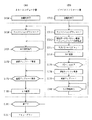
次に、図6を用いて、本実施形態によるリアルタイム制御システムに用いるデバイスコントローラの初期化処理について説明する。
図6は、本発明の一実施形態によるリアルタイム制御システムに用いるデバイスコントローラの初期化処理の内容を示すフローチャートである。図6において、図6(A)は、ホストコンピュータ10の初期化処理の内容を示し、図6(B)は、デバイスコントローラ100の初期化処理の内容を示している。
Next, the initialization process of the device controller used in the real-time control system according to the present embodiment will be described with reference to FIG.
FIG. 6 is a flowchart showing the contents of the initialization process of the device controller used in the real-time control system according to the embodiment of the present invention. 6A shows the contents of the initialization process of the
ステップs100において、ホストコンピュータ10の電源がONし、ステップs200において、デバイスコントローラ100の電源がONする。次に、ステップs105において、ホストコンピュータ10は、自己診断チェックなどのシステム初期化を行い、次に、ステップs110において、ディスクリプタセットアップを行う。同様にして、ステップs205において、デバイスコントローラ100は、自己診断チェックなどのシステム初期化を行い、次に、ステップs210において、ディスクリプタセットアップを行う。ディスクリプタセットアップは、USB通信の初期化で、ホストコンピュータ10とデバイスコントローラ100の間で通信を行うための初期設定などを行う。
In step s100, the
次に、ステップs115において、ホストコンピュータ10は、デバイスコントローラ100に対して、CPU初期化プログラムを転送し、ステップs120において、Ack受信待ちとなる。
Next, in step s115, the
一方、ステップs215において、デバイスコントローラ100のプロトコル処理部112は、ホストコンピュータ10から転送されたCPU初期化プログラムをダウンロードする。CPU初期化プログラムとは、デバイスコントローラ100のCPU初期化を行うためのプログラムで、CPU118の内蔵レジスタの設定を行う。ダウンロードしたプログラムは、ステップs220において、シリアルパラレル変換回路114は、ダウンロードした初期化プログラムをパラレルデータに変換して、キャッシュメモリ116にDMA転送する。次に、ステップs225において、プログラムカウンタコントローラ120は、CPUリセットを解除し、0番地に格納されているCPU初期化プログラムを実行する。なお、電源オンとなった時点で、リセット回路126は、CPU118をリセットしている。
On the other hand, in step s215, the
初期化が終了すると、ステップs230において、プログラムカウンタコントローラ120は、プログラムカウンタ122を「Loop」にセットする。
When the initialization is completed, in step s230, the
ここで、図7を用いて、本実施形態によるリアルタイム制御システムに用いるデバイスコントローラのキャッシュメモリ116の構成について説明する。
図7は、本発明の一実施形態によるリアルタイム制御システムに用いるデバイスコントローラのキャッシュメモリの構成を示すメモリマップである。
Here, the configuration of the
FIG. 7 is a memory map showing the configuration of the cache memory of the device controller used in the real-time control system according to one embodiment of the present invention.
キャッシュメモリ118の内容は、ファンクションエリアM10と、ワークエリアM30と、無限ループM40とが含まれている。ファンクションエリアM10の最後には無限ループへのジャンプ命令M20が書き込まれており、これにより無限ループM40へとジャンプし、ファンクションM10の処理が完了となる。
The contents of the
図6のステップs230の処理により、プログラムカウンタ122が「Loop」に設定されると、比較器124は、「Loop」に設定されたことを、プログラムカウンタコントローラ120に通知する。これを元に、ステップs235において、USBプロトコル処理部112は、ホストコンピュータ10にAckを送信する。
When the
ステップs120で説明したように、このとき、ホストコンピュータ10ではAck受信待ちとなっており、このAckを受信すると、ステップs125において、ホストコンピュータ10は、デバイスコントローラ100に対して、基板識別ファンクションを転送し、ステップs130において、Ack受信待ちとなる。
As described in step s120, at this time, the
一方、ステップs240において、デバイスコントローラ100のプロトコル処理部112は、ホストコンピュータ10から転送された基板識別ファンクションをダウンロードする。基板識別ファンクションとは、デバイスコントローラの拡張部に実装されている基板識別子を読み込むためのものである。ダウンロードしたプログラムは、ステップs245において、シリアルパラレル変換回路114は、ダウンロードした初期化プログラムをパラレルデータに変換して、キャッシュメモリ116にDMA転送する。次に、ステップs250において、プログラムカウンタコントローラ120は、プログラムカウンタ122を「Start」にセットする。そして、ステップs255において、USBプロトコル処理部112は、ホストコンピュータ10にAckを返答する。
On the other hand, in step s240, the
ステップs130で説明したように、このとき、ホストコンピュータ10ではAck受信待ちとなっており、Ackを受信すると、ステップs135において、返値アップロード要求を開始し、次に、ステップs140で返値アップロード待ちとなる。返値アップロード要求は、一定時間ごとに連続して送信され、デバイスコントローラ側で返値の準備ができていなければNACKを返信し、返値の準備ができれば返値とともにAck返答する。
As described in step s130, at this time, the
デバイスコントローラ側では、基板識別ファンクションをCPU118にて実行し、終了するとプログラムカウンタ122は「Loop」状態となる。そして、ステップs260において、プログラムカウンタコントローラ120は、「Loop」状態となったことを判別し、「Loop」状態となると、ステップs265において、シリアルパラレル変換回路114は、基板識別信号をシリアル変換し、ステップs270において、返値をホストコンピュータ10にアップロードする。
On the device controller side, the board identification function is executed by the
ホストコンピュータ10は返値を受け取ると、ステップs145において、デバイスコントローラ100にAckを送信し、ステップs150において、初期化完了となる。デバイスコントローラ100は、ステップs275において、Ack受信待ちとなっており、Ackを受信すると、ステップs280において、初期化完了となる。初期化が完了すると、デバイスコントローラ100は、ファンクション受付状態となる。
Upon receiving the return value, the
次に、図8及び図9を用いて、本実施形態によるリアルタイム制御システムにおけるファンクションの実行処理の内容について説明する。
図8は、本発明の一実施形態によるリアルタイム制御システムにおけるファンクションの実行処理の内容を示すフローチャートであり、図9は、本発明の一実施形態によるリアルタイム制御システムで用いられるファンクションの説明図である。図8において、図8(A)は、ホストコンピュータ10のファンクション転送処理の内容を示し、図8(B)は、デバイスコントローラ100のファンクション実行処理の内容を示している。
Next, the contents of the function execution process in the real-time control system according to the present embodiment will be described with reference to FIGS.
FIG. 8 is a flowchart showing the contents of function execution processing in the real-time control system according to the embodiment of the present invention. FIG. 9 is an explanatory diagram of functions used in the real-time control system according to the embodiment of the present invention. . 8A shows the contents of the function transfer process of the
ファンクション実行には、ステップs160において、ホストコンピュータ10は、デバイスコントローラ100に対して、ファンクションを転送し、ステップs165において、Ack受信待ちとなる。
For function execution, the
一方、ステップs300において、デバイスコントローラ100のプロトコル処理部112は、ホストコンピュータ10から転送されたファンクションをダウンロードする。
On the other hand, in step s300, the
ここで、図9を用いて、ファンクションの内容について説明する。本実施形態では、装置の制御をある一定時間で処理可能なファンクションに分割し、これをホストコンピュータ10からデバイスコントローラ100に送付することにより、システム全体としてリアルタイム性をもった制御システムを実現するようにしている。ここで、一定時間とは、例えば、1msである。リアルタイム制御を実行するためには、1ms程度で処理を完了する必要がある。一方、USBのデータ転送は、1ms周期で行われるため、ファンクションの実行時間を1msとすると、このデータ転送周期ともマッチングがとれる。
Here, the contents of the function will be described with reference to FIG. In this embodiment, the control of the apparatus is divided into functions that can be processed in a certain period of time, and this is sent from the
ホストコンピュータ側でリアルタイム制御可能な最小時間に収まる処理として、図9に示すように、初期化処理F10,バルブ開放処理7F20,アクチュエータ起動処理F30などがあり、これら一つ一つがファンクションとなる。ファンクションの処理内容としては、さらに時間の短いリアルタイム性が必要なI/O制御などが含まれ、デバイスコントローラ100で実行される。
As shown in FIG. 9, there are an initialization process F10, a valve opening process 7F20, an actuator activation process F30, and the like as processes within a minimum time that can be controlled in real time on the host computer side, and each of these functions. The processing contents of the function include I / O control that requires a shorter real time and is executed by the
例えば、バルブ開放処理F20をダウンロードしたデバイスコントローラ100は、処理f21において、流量計測定値をリードし、処理f22において、リードされた流量計測定値が正常値であるか否かを判断する。正常値でない場合には、処理f23において、返値=2として、終了する。
For example, the
正常値の場合には、処理f24において、次のDOライト(例えば、バルブ開放)処理を実行する。そして、処理f25において、DIリード(バルブ開放確認)処理を実行する。処理f26では、リードされたDIリード値が正常値か否かを判断する。正常値でない場合には、処理f27において、返値=3として、終了する。正常値の場合には、返値=1として、終了する。 In the case of a normal value, in the process f24, the next DO light (for example, valve opening) process is executed. In process f25, DI read (valve opening confirmation) process is executed. In process f26, it is determined whether or not the read DI read value is a normal value. If it is not a normal value, the process returns to step f27 with a return value = 3. If the value is normal, return value = 1 and the process ends.
これらの返値(=1,2,3)は、ホストコンピュータ10に送信され、ファンクションF20の実行結果がホストコンピュータ10に送信される。また、ADC(Analog Digital Converter)など、測定結果がある桁数の数値を取る場合などは、この値が返値としてホストコンピュータに送信される。
These return values (= 1, 2, 3) are transmitted to the
ファンクションを作成するにあたっては、装置のシステム設計段階において、ホストコンピュータにてリアルタイム制御可能な最小時間を1ファンクションタイムとし、これを基準として装置の処理を分割してゆく必要がある。なお、1ファンクションタイムを超える処理がある場合は動作開始と動作終了を二つのファンクションに分けるなどしてホストコンピュータにて実行管理を行う。 When creating a function, it is necessary to divide the processing of the apparatus on the basis of the minimum time that can be controlled in real time by the host computer as one function time in the system design stage of the apparatus. If there is processing that exceeds one function time, execution management is performed by the host computer by dividing the operation start and operation end into two functions.
再び、図8において、デバイスコントローラ100は、s300の処理によりファンクションをダウンロードすると、ダウンロードしたファンクションは、ステップs310において、シリアルパラレル変換回路114は、ダウンロードしたファンクションをパラレルデータに変換して、キャッシュメモリ116にDMA転送する。次に、ステップs315において、プログラムカウンタコントローラ120は、プログラムカウンタ122を「Start」にセットする。そして、ステップs320において、USBプロトコル処理部112は、ホストコンピュータ10にAckを返答する。
In FIG. 8 again, when the
ステップs165で説明したように、このとき、ホストコンピュータ10ではAck受信待ちとなっており、Ackを受信すると、ステップs170において、返値アップロード要求を開始し、次に、ステップs175で返値アップロード待ちとなる。返値アップロード要求は、一定時間ごとに連続して送信され、デバイスコントローラ側で返値の準備ができていなければNACKを返信し、返値の準備ができれば返値とともにAck返答する。
As described in step s165, at this time, the
デバイスコントローラ側では、ファンクションをCPU118にて実行し、終了するとプログラムカウンタ122は「Loop」状態となる。そして、ステップs325において、プログラムカウンタコントローラ120は、「Loop」状態となったことを判別し、「Loop」状態となると、ステップs330において、シリアルパラレル変換回路114は、返値をシリアル変換し、ステップs335において、返値をホストコンピュータ10にアップロードする。
On the device controller side, the function is executed by the
ホストコンピュータ10は返値を受け取ると、ステップs180において、デバイスコントローラ100にAckを送信する。デバイスコントローラ100は、ステップs340において、Ack受信待ちとなっており、Ackを受信すると、デバイスコントローラ100は、次のファンクション受付状態となる。
Upon receiving the return value, the
ホストコンピュータ10は、全てのファンクションが終了したか否かを判定して、終了すると、ステップs190において、シャットダウンする。
The
以上説明したように、本実施形態によれば、パーソナルコンピュータにおいて許容されているリアルタイム性を引き出し、下位のデバイスコントローラとバランスのよいリアルタイム制御システムを構築することができる。これにより双方でリソースが重複していた不揮発性メモリを減らすことができ、低コスト化を図ることができる。また、以前は生産時にロムライターやCPUのJTAG機能を用いていた不揮発性メモリ書き込みが不要となり、生産コストの低減を図れる。 As described above, according to the present embodiment, a real-time property allowed in a personal computer can be extracted, and a real-time control system with a good balance with a lower-level device controller can be constructed. As a result, it is possible to reduce the nonvolatile memory in which resources are duplicated on both sides, and to reduce the cost. In addition, non-volatile memory writing, which previously used the ROM tagwriter and CPU JTAG function at the time of production, is no longer necessary, and the production cost can be reduced.
また、デバイスコントローラを標準部と拡張部に分けたことにより、改廃のサイクルの短い部品を有する標準部については改廃するが、拡張部はそのまま利用することにより、デバイスコントローラをすべて作り直すといった作業量を減らすことができる。これにより、リアルタイム制御システムの開発から生産終了までの製品ライフサイクルにおけるコストの削減できる。
In addition, by dividing the device controller into a standard part and an extension part, the standard part with parts with a short cycle of revision and abolition will be abolished. Can be reduced. Thereby, the cost in the product life cycle from the development of the real-time control system to the end of production can be reduced.
10…ホストコンピュータ
30C…USB伝送線
100…デバイスコントローラ
110…デバイスコントローラ標準部
112…USBプロトコル処理部
114…シリアルパラレル変換回路
116…キャッシュメモリ
118…デバイスコントローラCPU
120…プログラムカウンタコントローラ
122…プログラムカウンタ
124…比較器
150…デバイスコントローラ拡張部
152…DI
154…DO
156…フィールドネットワークインタフェイス
158…モータコントローラ
160…モータドライバ
C10…標準部コネクタ
C20…拡張部コネクタ
DESCRIPTION OF
120 ...
154 ... DO
156: Field network interface 158:
Claims (8)
前記ホストコンピュータは、前記デバイスコントローラへの制御内容を、一定時間で処理可能なファンクションに分割して転送し、
前記デバイスコントローラは、前記ホストコンピュータから転送されたファンクションに基づいて、前記フィールドデバイスをリアルタイムで制御することを特徴とするリアルタイム制御システム。 In a real-time control system for controlling a field device in real time, comprising a host computer and a plurality of device controllers connected to the host computer and controlling field devices,
The host computer transfers the control content to the device controller by dividing it into functions that can be processed in a certain time,
The device controller controls the field device in real time based on a function transferred from the host computer.
前記デバイスコントローラは、それぞれ、共通な部品で構成される標準部と、接続されるフィールドデバイスによって異なる構成を持つ拡張部とから分割して構成され、前記標準部と前記拡張部とは、コネクタを介してバス接続されることを特徴とするリアルタイム制御システム。 The real-time control system according to claim 1,
Each of the device controllers is configured by dividing a standard part composed of common parts and an extension part having a different configuration depending on a connected field device, and the standard part and the extension part include connectors. A real-time control system characterized by being connected via a bus.
前記デバイスコントローラは、前記拡張部で保持している識別子を読み出し、前記ホストコンピュータに伝送し、
前記ホストコンピュータは、前記デバイスコントローラから転送された識別子に基づいて、複数の前記デバイスコントローラを識別することを特徴とするリアルタイム制御システム。 The real-time control system according to claim 2,
The device controller reads the identifier held in the extension unit, transmits it to the host computer,
The host computer identifies a plurality of the device controllers based on an identifier transferred from the device controller.
前記デバイスコントローラは、前記ホストコンピュータから転送されたファンクションを格納する揮発性メモリを備えたことを特徴とするリアルタイム制御システム。 The real-time control system according to claim 1,
The device controller comprises a volatile memory for storing a function transferred from the host computer.
前記ホストコンピュータは、前記デバイスコントローラに対し、前記ファンクションを一定周期で送付することを特徴とするリアルタイム制御システム。 The real-time control system according to claim 1,
The host computer sends the function to the device controller at a constant cycle.
前記ホストコンピュータは、USB(Universal Serial Bus)を用いて、前記デバイスコントローラに前記ファンクションを転送することを特徴とするリアルタイム制御システム。 The real-time control system according to claim 5, wherein
The real-time control system, wherein the host computer transfers the function to the device controller using a USB (Universal Serial Bus).
前記デバイスコントローラは、前記ファンクションを実行した結果を、返値として前記ホストコンピュータに送信することを特徴とするリアルタイム制御システム。 The real-time control system according to claim 1,
The device controller transmits a result of executing the function to the host computer as a return value.
前記ホストコンピュータ及び複数の前記デバイスコントローラは、ツリー型にネットワークにより接続されたことを特徴とするリアルタイム制御システム。
The real-time control system according to claim 1,
The real-time control system, wherein the host computer and the plurality of device controllers are connected by a network in a tree shape.
Priority Applications (1)
| Application Number | Priority Date | Filing Date | Title |
|---|---|---|---|
| JP2004108735A JP4418283B2 (en) | 2004-04-01 | 2004-04-01 | Real-time control system |
Applications Claiming Priority (1)
| Application Number | Priority Date | Filing Date | Title |
|---|---|---|---|
| JP2004108735A JP4418283B2 (en) | 2004-04-01 | 2004-04-01 | Real-time control system |
Publications (2)
| Publication Number | Publication Date |
|---|---|
| JP2005293333A true JP2005293333A (en) | 2005-10-20 |
| JP4418283B2 JP4418283B2 (en) | 2010-02-17 |
Family
ID=35326182
Family Applications (1)
| Application Number | Title | Priority Date | Filing Date |
|---|---|---|---|
| JP2004108735A Expired - Fee Related JP4418283B2 (en) | 2004-04-01 | 2004-04-01 | Real-time control system |
Country Status (1)
| Country | Link |
|---|---|
| JP (1) | JP4418283B2 (en) |
Cited By (3)
| Publication number | Priority date | Publication date | Assignee | Title |
|---|---|---|---|---|
| JP2009201245A (en) * | 2008-02-21 | 2009-09-03 | Toshiba Corp | Digital protective relay |
| JP2009258790A (en) * | 2008-04-11 | 2009-11-05 | Nst:Kk | Control device and control method of the same |
| US7786453B2 (en) | 2006-07-26 | 2010-08-31 | Nuflare Technology, Inc. | Charged-particle beam pattern writing method and apparatus with a pipeline process to transfer data |
-
2004
- 2004-04-01 JP JP2004108735A patent/JP4418283B2/en not_active Expired - Fee Related
Cited By (3)
| Publication number | Priority date | Publication date | Assignee | Title |
|---|---|---|---|---|
| US7786453B2 (en) | 2006-07-26 | 2010-08-31 | Nuflare Technology, Inc. | Charged-particle beam pattern writing method and apparatus with a pipeline process to transfer data |
| JP2009201245A (en) * | 2008-02-21 | 2009-09-03 | Toshiba Corp | Digital protective relay |
| JP2009258790A (en) * | 2008-04-11 | 2009-11-05 | Nst:Kk | Control device and control method of the same |
Also Published As
| Publication number | Publication date |
|---|---|
| JP4418283B2 (en) | 2010-02-17 |
Similar Documents
| Publication | Publication Date | Title |
|---|---|---|
| CN113872796B (en) | Method, device, equipment and medium for acquiring information of server and node equipment thereof | |
| US4622633A (en) | Object building method for self configuring computer network | |
| US4635192A (en) | Self configuring bus structure for computer network | |
| JPH05158511A (en) | Programmable controller processor having attaching and removing type function card | |
| US8543976B1 (en) | Generation of multi-domain code from a graphical program | |
| CN102902650A (en) | Data sharing and transmission system and method | |
| US20140359189A1 (en) | Systems and methods for providing connections to an information handling system | |
| US20170039151A1 (en) | Universal intelligent platform management interface (ipmi) host to baseboard management controller (bmc) communication for non-x86 and legacy free systems | |
| CN106598898A (en) | System and method for sharing bus port | |
| US10963406B2 (en) | Persistent universal serial bus (USB) device enumeration | |
| JP4418283B2 (en) | Real-time control system | |
| EP3382567B1 (en) | Multiple storage devices implemented using a common connector | |
| KR20070108410A (en) | Method and apparatus for independent and simultaneous data transfer on host controller | |
| JPH03196225A (en) | Programmable interrupt controller | |
| JP4359618B2 (en) | Configuration register access method, setting method, integrated circuit parts, computer system, product | |
| KR950008229B1 (en) | Personal computer with local bus arbitration | |
| EP4675454A1 (en) | Processor platform, circuit board, and server | |
| CN113824741A (en) | IIC device communication method, apparatus, device, system and medium | |
| TWI749658B (en) | Usb hub device having functionality of self firmware updating and host system having the same | |
| JP2940841B2 (en) | Processor module for programmable controller | |
| JP2002342256A (en) | Data processor and data table updating method | |
| JP2582504B2 (en) | Personal computer system | |
| CN113806282A (en) | Heterogeneous control system and loading method thereof | |
| CN202615386U (en) | Single board and data processing system | |
| CN112416832B (en) | Communication system based on MIPS architecture processor |
Legal Events
| Date | Code | Title | Description |
|---|---|---|---|
| A621 | Written request for application examination |
Free format text: JAPANESE INTERMEDIATE CODE: A621 Effective date: 20060525 |
|
| A977 | Report on retrieval |
Free format text: JAPANESE INTERMEDIATE CODE: A971007 Effective date: 20081111 |
|
| A131 | Notification of reasons for refusal |
Free format text: JAPANESE INTERMEDIATE CODE: A131 Effective date: 20081118 |
|
| A521 | Request for written amendment filed |
Free format text: JAPANESE INTERMEDIATE CODE: A523 Effective date: 20090116 |
|
| A131 | Notification of reasons for refusal |
Free format text: JAPANESE INTERMEDIATE CODE: A131 Effective date: 20090623 |
|
| A521 | Request for written amendment filed |
Free format text: JAPANESE INTERMEDIATE CODE: A523 Effective date: 20090701 |
|
| TRDD | Decision of grant or rejection written | ||
| A01 | Written decision to grant a patent or to grant a registration (utility model) |
Free format text: JAPANESE INTERMEDIATE CODE: A01 Effective date: 20091124 |
|
| A01 | Written decision to grant a patent or to grant a registration (utility model) |
Free format text: JAPANESE INTERMEDIATE CODE: A01 |
|
| A61 | First payment of annual fees (during grant procedure) |
Free format text: JAPANESE INTERMEDIATE CODE: A61 Effective date: 20091127 |
|
| R150 | Certificate of patent or registration of utility model |
Ref document number: 4418283 Country of ref document: JP Free format text: JAPANESE INTERMEDIATE CODE: R150 Free format text: JAPANESE INTERMEDIATE CODE: R150 |
|
| FPAY | Renewal fee payment (event date is renewal date of database) |
Free format text: PAYMENT UNTIL: 20121204 Year of fee payment: 3 |
|
| FPAY | Renewal fee payment (event date is renewal date of database) |
Free format text: PAYMENT UNTIL: 20131204 Year of fee payment: 4 |
|
| S531 | Written request for registration of change of domicile |
Free format text: JAPANESE INTERMEDIATE CODE: R313531 |
|
| S533 | Written request for registration of change of name |
Free format text: JAPANESE INTERMEDIATE CODE: R313533 |
|
| R350 | Written notification of registration of transfer |
Free format text: JAPANESE INTERMEDIATE CODE: R350 |
|
| LAPS | Cancellation because of no payment of annual fees |