JP2005293300A - Set associative cache system and control method of cache memory - Google Patents
Set associative cache system and control method of cache memory Download PDFInfo
- Publication number
- JP2005293300A JP2005293300A JP2004108286A JP2004108286A JP2005293300A JP 2005293300 A JP2005293300 A JP 2005293300A JP 2004108286 A JP2004108286 A JP 2004108286A JP 2004108286 A JP2004108286 A JP 2004108286A JP 2005293300 A JP2005293300 A JP 2005293300A
- Authority
- JP
- Japan
- Prior art keywords
- cache
- way
- block
- address
- information
- Prior art date
- Legal status (The legal status is an assumption and is not a legal conclusion. Google has not performed a legal analysis and makes no representation as to the accuracy of the status listed.)
- Granted
Links
Images


Classifications
-
- G—PHYSICS
- G06—COMPUTING OR CALCULATING; COUNTING
- G06F—ELECTRIC DIGITAL DATA PROCESSING
- G06F12/00—Accessing, addressing or allocating within memory systems or architectures
- G06F12/02—Addressing or allocation; Relocation
- G06F12/08—Addressing or allocation; Relocation in hierarchically structured memory systems, e.g. virtual memory systems
- G06F12/12—Replacement control
- G06F12/121—Replacement control using replacement algorithms
- G06F12/123—Replacement control using replacement algorithms with age lists, e.g. queue, most recently used [MRU] list or least recently used [LRU] list
Landscapes
- Engineering & Computer Science (AREA)
- Theoretical Computer Science (AREA)
- Physics & Mathematics (AREA)
- General Engineering & Computer Science (AREA)
- General Physics & Mathematics (AREA)
- Memory System Of A Hierarchy Structure (AREA)
Abstract
Description
本発明は、キャッシュブロック数を一定数に維持したままセット数とウェイ数とを変更することができるセットアソシアティブキャッシュシステム及びキャッシュメモリの制御方法に関する。 The present invention relates to a set associative cache system and a cache memory control method capable of changing the number of sets and the number of ways while maintaining the number of cache blocks at a fixed number.
現在、システムの複雑化、半導体技術の向上により、マルチタスクOS、マルチプロセッサ、マルチスレッドプロセッサ、オンチップマルチプロセッサ等の技術が構築可能になっている。さらに最近の傾向として、複数のシステムの小型化、資源の共有化の思想が尊重され、様々な発明が提案されている。そのような環境下でキャッシュの共有化の発明も盛んに提案されている。キャッシュの共有化で課題となることは、処理の複雑化に対応して、如何に性能が良いキャッシュシステムを構築するかにある。 Currently, with the complexity of the system and the improvement of semiconductor technology, technologies such as a multitask OS, a multiprocessor, a multithread processor, and an on-chip multiprocessor can be constructed. Furthermore, as a recent trend, various inventions have been proposed with respect to the idea of downsizing a plurality of systems and sharing resources. In such an environment, inventions for sharing a cache have been actively proposed. The problem with cache sharing is how to build a cache system with good performance in response to the complexity of processing.
キャッシュの性能を高めるため、システム単位の処理、プロセッサ単位の処理、スレッド単位の処理にキャッシュ領域を分割したキャッシュが提案されている。しかし、これらの分割手法は、以下の課題がある。 In order to improve the performance of the cache, a cache in which a cache area is divided into processing in units of systems, processing in units of processors, and processing in units of threads has been proposed. However, these division methods have the following problems.
キャッシュセットで分割するタイプ
・ 領域を分割した場合、キャッシュブロックをそのまま利用できないのでキャッシュミスが発生する(課題1)。
キャッシュウェイで分割するタイプ
・ ウェイ数が不足して処理単位内での競合ミスが発生することがある(課題2)。
・ 処理単位数を増減して領域を変更する場合、処理単位間の競合ミスが発生する(課題3)。
キャッシュブロック単位で分割するタイプ
・ 処理単位数の増減に関わらず、処理単位間の競合ミスが発生する(課題4)。
Type of partitioning by cache set-When an area is partitioned, a cache miss occurs because the cache block cannot be used as it is (Problem 1).
Types divided by cash ways • There may be a conflict number in the processing unit due to insufficient number of ways (Problem 2).
-When changing the area by increasing or decreasing the number of processing units, a contention error between processing units occurs (Problem 3).
Type of partitioning in units of cache blocks ・ A conflict error occurs between processing units regardless of the increase or decrease in the number of processing units (Problem 4).
さらに改良型のキャッシュシステムとして、ウェイ数を指定可能とし、さらに、ウェイ数に応じたヒットチェックを行うように構成することにより、プログラム単位でのキャッシュミスを減らす技術が特許文献1に開示されている。
また、ウェイ数の指定を可能とし、タスク間のキャッシュミスを減らす技術が特許文献2に開示されている。
Further, as an improved cache system,
Further,
特許文献1と2とに開示されたキャッシュシステムは、シングルプロセッサのための技術であり、マルチタスクOS、マルチプロセッサ、マルチスレッドのための技術ではない。従って、これらの技術では、マルチタスクOS、マルチプロセッサ、マルチスレッド下ではキャッシュミスを減らすことができない。
また、特許文献1と2とに開示されたウェイ選択・比較方法は、キャッシュ要求時のウェイの最大値を指定する手法であり、最大構成より少ないウェイ数の構成にした時に使用されないキャッシュ容量が発生し、キャッシュの使用効率が低い。
The way selection / comparison methods disclosed in
この発明は上記実情に鑑みてなされたものであり、セット数やウェイ数を変更しても、同一キャッシュアドレスに対応するキャッシュブロックの位置・範囲が変わらないセットアソシアティブキャッシュシステムなどを提供することを目的とする。
また、この発明は、セット数やウェイ数を変更しても、利用可能なキャッシュ容量が減少しないセットアソシアティブキャッシュシステムなどを提供することを目的とする。
The present invention has been made in view of the above circumstances, and provides a set associative cache system in which the position and range of cache blocks corresponding to the same cache address does not change even if the number of sets or the number of ways is changed. Objective.
It is another object of the present invention to provide a set associative cache system in which the available cache capacity does not decrease even if the number of sets or the number of ways is changed.
上記目的を達成するため、本発明の第1の観点に係るセットアソシアティブキャッシュシステムは、
i組のmウェイnセットのキャッシュメモリと、
キャッシュアドレスとキャッシュ管理情報に基づいて、前記i組のキャッシュメモリの全部又は1つを選択し、キャッシュアドレスに従って、選択したキャッシュメモリのうちの第jのセットを選択するセット選択手段と、
キャッシュ管理情報に基づいてウェイを選択するウェイ選択手段と、
前記セット選択手段により選択されたセットの前記ウェイ選択手段で選択したウェイのキャッシュブロックのブロックアドレスとキャッシュブロックのブロックアドレスとを比較し、キャッシュヒットとミスとの別を判定する判定手段と、
前記判定手段の判定結果に基づいて、置き換えブロックを選択する置き換え選択手段と、
を具備することを特徴とする。
In order to achieve the above object, a set associative cash system according to the first aspect of the present invention provides:
i sets of m-way n sets of cache memory;
Set selection means for selecting all or one of the i sets of cache memories based on a cache address and cache management information, and selecting a jth set of the selected cache memories according to the cache address;
Way selection means for selecting a way based on cache management information;
A determination unit that compares the block address of the cache block of the way selected by the way selection unit of the set selected by the set selection unit with the block address of the cache block, and determines whether the cache hit is a miss or
Replacement selection means for selecting a replacement block based on the determination result of the determination means;
It is characterized by comprising.
例えば、前記キャッシュアドレスは、ブロックアドレスとセットアドレスとを含み、前記キャッシュ管理情報は、処理単位に関する情報を含む。前記処理単位に関する情報とは、例えば、システムの状態(論理的なシステムの数、キャッシュを要求したシステムの番号)を示す情報、プロセスの状態(論理的なプロセスの数、キャッシュを要求したプロセスの番号)を示す情報、スレッドの状態(論理的なスレッド数、キャッシュを要求したスレッドの番号)を示す情報、メモリの共有の状態を示す情報を含む。 For example, the cache address includes a block address and a set address, and the cache management information includes information on a processing unit. The information on the processing unit includes, for example, information indicating the state of the system (the number of logical systems and the number of the system that requested the cache), the state of the process (the number of logical processes, the number of processes that requested the cache) Number), information indicating the thread state (the number of logical threads, the number of the thread that requested the cache), and information indicating the memory sharing state.
前記ウェイ選択手段は、例えば、前記キャッシュ管理情報と共にキャッシュブロックのLRU情報に基づいて、ウェイを選択し、前記置き換え選択手段は、前記キャッシュ管理情報と共にキャッシュブロックのLRU情報に基づいて、置き換えブロックを選択する。 The way selection means, for example, selects a way based on cache block LRU information together with the cache management information, and the replacement selection means selects a replacement block based on cache block LRU information together with the cache management information. select.
また、前記ウェイ選択手段は、前記キャッシュ管理情報と共にキャッシュブロックのLRU情報とさらに各ウェイへの処理の割り当ての情報に基づいて、ウェイを選択し、前記置き換え選択手段は、前記キャッシュ管理情報と共にキャッシュブロックのLRU情報とさらに各ウェイへの処理の割り当ての情報に基づいて、置き換えブロックを選択する。 The way selection means selects a way based on the cache management information and the LRU information of the cache block and further information on the allocation of processing to each way, and the replacement selection means caches the cache management information together with the cache management information. A replacement block is selected on the basis of the LRU information of the block and information on the allocation of processing to each way.
上述の制御により、上記キャッシュシステムは、例えば、mウェイi・nセットのセットアソシアティブキャッシュと、i・mウェイnセットのセットアソシアティブキャッシュと、として機能する。 With the above-described control, the cache system functions as, for example, an m-way i · n set set associative cache and an i · m way n set set associative cache.
この場合、セット数とウェイ数とを変更しても、同一のキャッシュアドレスに対応するキャッシュブロックの位置が変化しない。また、セット数とウェイ数とを変更しても、利用可能なキャッシュ容量が変化しない。 In this case, even if the number of sets and the number of ways are changed, the position of the cache block corresponding to the same cache address does not change. Further, even if the number of sets and the number of ways are changed, the available cache capacity does not change.
上記目的を達成するため、本発明の第2の観点に係るキャッシュメモリの制御方法は、
i組のmウェイnセットのキャッシュメモリについて、
キャッシュアドレスとキャッシュ管理情報に基づいて、前記i組のキャッシュメモリの全部又は1つを選択し、キャッシュアドレスに従って、選択したキャッシュメモリのうちの第jのセットを選択し、
キャッシュ管理情報に基づいてウェイを選択し、
選択したセットの選択したウェイのキャッシュブロックのブロックアドレスと、キャッシュアドレス中の要求ブロックアドレスとを比較し、キャッシュヒットとミスとを判定し、
判定結果に基づいて、置き換えブロックを選択する、
ことを特徴とする。
In order to achieve the above object, a cache memory control method according to a second aspect of the present invention includes:
About i sets of m-way n-set cache memories
Selecting all or one of the i sets of cache memories based on a cache address and cache management information, and selecting a jth set of the selected cache memories according to the cache address;
Select way based on cache management information,
Compare the block address of the cache block of the selected way of the selected set with the requested block address in the cache address, determine the cache hit and miss,
Based on the determination result, select a replacement block.
It is characterized by that.
上記構成とすることにより、この発明によれば、セット数とウェイ数とを適宜変更してキャッシュシステムを使用できる。 With the above configuration, according to the present invention, the cache system can be used by appropriately changing the number of sets and the number of ways.
(実施形態1)
以下、この発明の実施の形態に係るキャッシュシステムを説明する。このキャッシュシステムは、処理単位(システム、プロセス、スレッド)に応じてキャッシュ構成を変更できる可変mウェイnセットアソシアティブキャッシュである。
(Embodiment 1)
Hereinafter, a cache system according to an embodiment of the present invention will be described. This cache system is a variable m-way n-set associative cache that can change a cache configuration according to a processing unit (system, process, thread).
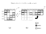
図1に本実施の形態のキャッシュシステムの概要を示す。図1(a)に示すキャッシュシステム101は4セット4ウェイアソシアティブキャッシュで、キャッシュブロックには処理単位1のメモリブロックの写しが書き込まれている。一方、図1(b)に示すキャッシュシステム102はキャッシュシステム101の構成を変更した後の状態で2セット8ウェイアソシアティブキャッシュである。キャッシュブロックには処理単位1と処理単位2のメモリブロックの写しが書き込まれていて、各セット内のブロックは処理単位1と処理単位2とで2分割されている。
FIG. 1 shows an overview of the cache system of the present embodiment. The cache system 101 shown in FIG. 1A is a 4-set 4-way associative cache, and a copy of the memory block of
但し、図1(a)と(b)とで、処理1のメモリブロックの写しのキャッシュブロック上の位置は、符号1−1〜1−8で示すように変化していない。
However, in FIGS. 1A and 1B, the position of the copy of the memory block of
このように、本実施の形態のキャッシュシステムは処理単位に応じて各セット内をブロック単位で分割でき、ウェイ数とセット数とを変更できる。 As described above, the cache system according to the present embodiment can divide each set in units of blocks according to the processing unit, and can change the number of ways and the number of sets.
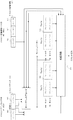
図2はプロセッサ構成を示している。プロセッサチップ200は、プロセッサコア210とプロセッサコア220とキャッシュコントローラ230と2−4セット4−2ウェイアソシアティブキャッシュ240で構成されている。
FIG. 2 shows the processor configuration. The processor chip 200 includes a
プロセッサコア210はマルチスレッドアーキテクチャ機能を有し、実質的に同時に複数(本実施の形態では2)スレッドを処理できる。ここでのスレッドとはハードウエアが同時に処理できる命令列のことを意味する。
また、プロセッサチップ200は論理的にシステム数を複数(本実施の形態では2)に分割できる。
The
Further, the processor chip 200 can logically divide the number of systems into a plurality (2 in this embodiment).
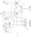
図3は、図2に示すプロセッサチップ200に組み込まれている2−4セット4−2ウェイアソシアティブキャッシュ240の構成例を示す。
この2−4セット4−2ウェイアソシアティブキャッシュ240は、キャッシュコントローラ230からの指示により、2セット4ウェイアソシアティブ構成と4セット2ウェイアソシアティブ構成とで切り替えることができるキャッシュである。
FIG. 3 shows a configuration example of the 2-4 set 4-2 way
The 2-4 set 4-2 way
図示するように、このキャッシュ240は、キャッシュアドレスレジスタA−REGとキャッシュ管理情報レジスタM−REGと、セットアドレスデコーダ320と、キャッシュアレイ330と、キャッシュアレイ340と、比較回路350と、から構成されている。
As shown in the figure, the
キャッシュアドレスレジスタA−REGは、キャッシュコントローラ230から供給されるキャッシュアドレス300を格納する。
The cache address register A-REG stores the cache address 300 supplied from the
キャッシュアドレス300は、ブロックアドレス301とセットアドレス302とブロック内アドレスとからなる。ブロックアドレス301とセットアドレス302との幅はセット数(この例では、4セットと2セットの別)に応じて変化する。
The cache address 300 includes a
ブロックアドレス301は、4セットの場合には1ビット、2セットの場合には2ビットであり、4セットの場合には、「0」と「1」で、各セット内の第1ブロックと第2ブロックとを示す。一方、2セットの場合には、「00」、「01」、「10」、「11」で、各セット内の第1〜第4ブロックを示す。
The
セットアドレス302は、4セットの場合には2ビット、2セットの場合には1ビットであり、4セットの場合には、「00」、「01」、「10」、「11」で、第1〜第4セットを示し、2セットの場合には、「0」と「1」で、第1セットと第2セットとを示す。
The
また、キャッシュ管理情報310は、ソフトウエア(SW)、ファームウエア(FW)、又はハードウエア(HW)により設定され、実施例では、システム番号311と、スレッド番号312と、メモリ共有情報313とから構成されている。
The cache management information 310 is set by software (SW), firmware (FW), or hardware (HW). In the embodiment, the cache management information 310 includes a system number 311, a thread number 312, and memory shared
システム番号311は、キャッシュ要求時点でのシステムの数(論理数)とキャッシュを要求したシステムの番号とを含む。スレッド番号312は、キャッシュ要求時点でのスレッドの数とキャッシュを要求したスレッドの番号を含む。メモリ共有情報313は、メモリを共有しているスレッドを特定する情報を提供する。
The system number 311 includes the number of systems (logical number) at the time of the cache request and the number of the system that requested the cache. The thread number 312 includes the number of threads at the time of the cache request and the number of the thread that requested the cache. The
例えば、図2に示すプロセッサコア210と220とにより、システムが論理的に2つに分割されており、2つのうちの第1番のシステムがキャッシュを要求した場合には、システム番号311は、キャッシュ要求時点でのシステムの数(論理数)が2となり、キャッシュを要求したシステムの番号は「1」となる。
For example, when the system is logically divided into two by the
さらに、図2に示すプロセッサコア210と220とにより、3つのスレッドが並行して実行されており、第2番のスレッドがキャッシュを要求した場合には、スレッド番号312のスレッド数は3、キャッシュを要求したスレッドの番号は「2」となる。
さらに、あるスレッドがメモリを共有している場合には、そのスレッドの番号がメモリ共有情報313に設定される。
Further, when three threads are executed in parallel by the
Furthermore, when a certain thread shares memory, the thread number is set in the
セットアドレスデコーダ320は、キャッシュアドレス300とキャッシュ管理情報310とを入力とし、対象セットを選択する。デコードのルールについては、後述する。 The set address decoder 320 receives the cache address 300 and the cache management information 310 and selects a target set. Decoding rules will be described later.
キャッシュアレイ330、340は、それぞれ、4つのキャッシュブロックから構成されている。各キャッシュブロックは、セット1〜4、ウェイ1〜4のいずれかに割り当てられている。
Each of the
セットアドレスデコーダ320によりセットが選択され、キャッシュアレイ330、340は、選択されたセットに書き込まれているブロックアドレスを比較回路350に出力する。キャッシュアレイ330、340には最大幅のブロックアドレスが常に書き込まれる。比較回路350はブロックアドレス301とキャッシュ管理情報310とを入力とし、キャッシュのミスヒット判定を行う。
The set is selected by the set address decoder 320, and the
図4は比較回路350を詳細に示した図である。ウェイ選択回路410はキャッシュ管理情報310とLRUビット400とから、各処理単位が利用できるウェイ領域を選択する。LRUビット400の拡張ビットにはキャッシュ要求時点でのウェイ分割状態が保存されており、ウェイ選択回路410はLRUビット400の拡張ビットに格納されているウェイ分割状態に従って、キャッシュ要求時点でのセット数とウェイ数の状態を判別する。比較部420と比較部430はキャッシュアドレス300のブロックアドレス301とキャッシュアレイ330、340のブロックアドレスとウェイ選択回路410のウェイ領域とを比較してヒット判定回路440によってミス/ヒット判定を行う。置き換え選択回路450は、キャッシュミス時に置き換えるキャッシュブロックを選択する。実施例では、システム数が1の時は、4セット2ウェイアソシアティブキャッシュ構成で、システム数が2の時は2セット4ウェイアソシアティブキャッシュ構成とし、スレッド数に応じてウェイを分割するものとする。
FIG. 4 shows the
(動作の説明)
2−4セット4−2ウェイアソシアティブキャッシュの動作の説明をする。図5はキャッシュ要求でセットアドレス302とキャッシュ管理情報310とからセットとウェイとの領域を決定するセットアドレスデコーダ320とウェイ選択回路410の動作結果とを表している。アクセス1から2は、4セット2ウェイアソシアティブキャッシュ構成で、アクセス3から6は、2セット4ウェイアソシアティブキャッシュ構成となる。
(Description of operation)
The operation of the 2-4 set 4-2 way associative cache will be described. FIG. 5 shows the operation results of the set address decoder 320 and the
アクセス1の場合、セットアドレスデコーダ320はシステム番号311のシステム数が1の時、セットアドレス302の2ビット“11”からセット4を選択する。一方、ウェイ選択回路410はスレッド番号312のスレッド番号が1の時、LRUビット400の拡張ビットからセット4のウェイ3を選択する。LRUビット400のLRUビットは更新され、拡張ビットの更新は、スレッド数が増減した時に行われるので更新されない。
In the case of
アクセス2の場合、セット4、ウェイ4が選択される。LRUビット400のLRUビットは更新され、拡張ビットは更新されない。
In the case of
アクセス3の場合、セットアドレスデコーダ320はシステム番号311のシステム数が2の時、セットアドレス302の1ビット“1”からセット2とセット4を選択する(ウェイ数が2から4となる)。一方、ウェイ選択回路410はスレッド数が2から3となるので、LRUビット400のLRUビットが示している内容からウェイ2を選択し、LRUビットと拡張ビットの更新を行う。
In the case of
アクセス4の場合、セット2、4とウェイ3とが選択される。LRUビットの更新を行い、拡張ビットの更新は行わない。
For
アクセス5の場合、セット2、4が選択される。ウェイ選択回路410はスレッド数が3から4となるので、LRUビット400の拡張ビットに格納されている内容からセット1とセット3とを選び、LRUビットからウェイ1を選択し、LRUビットと拡張ビットとの更新を行う。
アクセス5の場合、スレッド3とスレッド4とがメモリ共有されている。そのことを示す情報がメモリ共有情報310にセットされている。メモリ共有情報310は、ヒット判定回路440に入力され、結局、ウェイ1とウェイ2とがヒット判定対象キャッシュブロックとなる。
For
In the case of
アクセス6の場合、セット2、4とウェイ4とが選択される。LRUビットの更新を行い、拡張ビットの更新は行わない。
For access 6, sets 2, 4 and
上記の説明のようにキャッシュシステムを構成して駆動することにより、以下の効果が得られる。
ウェイ数を増やせるので、処理単位内及び処理単位間での競合ミスを防ぐ(効果1)。
セット数とウェイ数を変更してもキャッシュアドレスが指すキャッシュブロックの位置が変わらないのでキャッシュ区分領域変更でのキャッシュミスを低減できる(効果2)。
各ウェイの領域を変更する時にLRUビットを参照することによって区分領域を決定するので処理単位間での競合ミスを低減することができる(効果3)。
By configuring and driving the cache system as described above, the following effects can be obtained.
Since the number of ways can be increased, contention errors within and between processing units are prevented (effect 1).
Even if the number of sets and the number of ways are changed, the position of the cache block pointed to by the cache address does not change, so cache misses caused by changing the cache partition area can be reduced (Effect 2).
Since the divided area is determined by referring to the LRU bit when changing the area of each way, it is possible to reduce contention errors between processing units (effect 3).
なお、この発明は上記実施の形態に限定されず、種々の変形及び応用が可能である。
例えば、図1の構成では、4ブロック(2セット×2ウェイ)のキャッシュアレイを2セット(330と340)用意し、セットの選択とウェイの選択とを制御することにより、4セット×2ウェイ(セット1、セット2、セット3、セット4、各セット1と2とについてはウェイ1とウェイ2、セット3と4とについては、ウェイ3と4)と、2セット×4ウェイ(セット1とセット3とからなる第1のセット、セット2とセット4とからなる第2のセット;第1のセットと第2のセットはそれぞれウェイ1〜ウェイ4)とを切り替えたが、構成は任意である。
In addition, this invention is not limited to the said embodiment, A various deformation | transformation and application are possible.
For example, in the configuration of FIG. 1, two sets (330 and 340) of a cache array of 4 blocks (2 sets × 2 ways) are prepared, and 4 sets × 2 ways are controlled by controlling the selection of the set and the selection of the way. (
m(2の乗数)ウェイ・n(2の乗数)セットのキャッシュメモリ(図1のキャッシュアレイ330、340に相当するものをi(2の乗数)個用意し、セットアドレスデコーダが、キャッシュアドレスとキャッシュ管理情報とに基づいて、i組のキャッシュメモリの全部又は1つを選択し、選択したキャッシュメモリのうちの第jのセットを選択し、ウェイ選択回路が、キャッシュ管理情報とLRUビットとに基づいてウェイを選択し、比較部は、k個配置されて対応するウェイ上の選択されたセットのキャッシュブロックのブロックアドレスと要求ブロックアドレスとを比較してヒット判定を行い、置き換え選択回路がウェイ選択回路の出力とヒット・ミスヒットを示す情報とに基づいて置き換えブロックを選択する。
m (multiplier of 2) ways and n (multiplier of 2) sets of cache memories (i (multiplier of 2)) corresponding to the
このような構成により、例えば、mウェイi・nセットのセットアソシアティブキャッシュ、と、i・mウェイnセットのセットアソシアティブキャッシュ、との可変セットアソシアティブキャッシュシステムを得ることができる。 With such a configuration, for example, a variable set associative cache system including an m-way i · n set set associative cache and an i · m way n set set associative cache can be obtained.
この場合、セット数とウェイ数とを変更しても、同一のキャッシュアドレスに対応するキャッシュブロックの位置が変化しない。また、セット数とウェイ数とを変更しても、利用可能なキャッシュ容量が変化しない。 In this case, even if the number of sets and the number of ways are changed, the position of the cache block corresponding to the same cache address does not change. Further, even if the number of sets and the number of ways are changed, the available cache capacity does not change.
101・・・キャッシュシステム、102・・・キャッシュシステム、200・・・プロセッサチップ、210・・・プロセッサコア、220・・・プロセッサコア、230・・・キャッシュコントローラ、240・・・キャッシュ、300・・・キャッシュアドレス、310・・・キャッシュ管理情報、320・・・セットアドレスデコーダ、330・・・キャッシュアレイ、340・・・キャッシュアレイ、350・・・比較回路、400・・・LRUビット、410・・・ウェイ選択回路、420・・・比較部、430・・・比較部、440・・・ヒット判定回路、450・・・置き換え選択回路
DESCRIPTION OF SYMBOLS 101 ... Cache system, 102 ... Cache system, 200 ... Processor chip, 210 ... Processor core, 220 ... Processor core, 230 ... Cache controller, 240 ... Cache, 300 ..Cache address 310 ... Cache management information 320 ... Set
Claims (9)
キャッシュアドレスとキャッシュ管理情報に基づいて、前記i組のキャッシュメモリの全部又は1つを選択し、キャッシュアドレスに従って、選択したキャッシュメモリのうちの第jのセットを選択するセット選択手段と、
キャッシュ管理情報に基づいてウェイを選択するウェイ選択手段と、
前記セット選択手段により選択されたセットの前記ウェイ選択手段で選択したウェイのキャッシュブロックのブロックアドレスとキャッシュブロックのブロックアドレスとを比較し、キャッシュヒットとミスとの別を判定する判定手段と、
前記判定手段の判定結果に基づいて、置き換えブロックを選択する置き換え選択手段と、
を具備することを特徴とするセットアソシアティブキャッシュシステム。 i sets of m-way n sets of cache memory;
Set selection means for selecting all or one of the i sets of cache memories based on a cache address and cache management information, and selecting a jth set of the selected cache memories according to the cache address;
Way selection means for selecting a way based on cache management information;
A determination unit that compares the block address of the cache block of the way selected by the way selection unit of the set selected by the set selection unit with the block address of the cache block, and determines whether the cache hit is a miss or
Replacement selection means for selecting a replacement block based on the determination result of the determination means;
A set associative cache system comprising:
前記キャッシュ管理情報は、処理単位に関する情報を含む、
ことを特徴とする請求項1に記載のセットアソシアティブキャッシュシステム。 The cache address includes a block address and a set address,
The cache management information includes information on a processing unit.
The set associative cache system according to claim 1.
ことを特徴とする請求項2に記載のセットアソシアティブキャッシュシステム。 The information on the processing unit includes information indicating a system state, information indicating a process state, information indicating a thread state, and information on sharing a memory.
The set associative cache system according to claim 2.
前記置き換え選択手段は、前記キャッシュ管理情報と共にキャッシュブロックのLRU情報に基づいて、置き換えブロックを選択する、
ことを特徴とする請求項1、2又は3のいずれか1項に記載のセットアソシアティブキャッシュシステム。 The way selection means selects a way based on LRU information of the cache block together with the cache management information,
The replacement selection means selects a replacement block based on LRU information of the cache block together with the cache management information.
The set associative cache system according to any one of claims 1, 2, and 3.
前記置き換え選択手段は、前記キャッシュ管理情報と共にキャッシュブロックのLRU情報とさらに各ウェイへの処理の割り当ての情報に基づいて、置き換えブロックを選択する、
ことを特徴とする請求項1、2又は3のいずれか1項に記載のセットアソシアティブキャッシュシステム。 The way selection means selects a way based on LRU information of the cache block together with the cache management information and information of processing allocation to each way,
The replacement selection means selects a replacement block based on LRU information of the cache block together with the cache management information and information on processing allocation to each way.
The set associative cache system according to any one of claims 1, 2, and 3.
キャッシュアドレスとキャッシュ管理情報に基づいて、前記i組のキャッシュメモリの全部又は1つを選択し、キャッシュアドレスに従って、選択したキャッシュメモリのうちの第jのセットを選択し、
キャッシュ管理情報に基づいてウェイを選択し、
選択したセットの選択したウェイのキャッシュブロックのブロックアドレスと、キャッシュアドレス中の要求ブロックアドレスとを比較し、キャッシュヒットとミスとを判定し、
判定結果に基づいて、置き換えブロックを選択する、
ことを特徴とするセットアソシアティブキャッシュメモリの制御方法。 About i sets of m-way n-set cache memories
Selecting all or one of the i sets of cache memories based on a cache address and cache management information, and selecting a jth set of the selected cache memories according to the cache address;
Select way based on cache management information,
Compare the block address of the cache block of the selected way of the selected set with the requested block address in the cache address, determine the cache hit and miss,
Based on the determination result, select a replacement block.
A method for controlling a set associative cache memory.
Priority Applications (2)
| Application Number | Priority Date | Filing Date | Title |
|---|---|---|---|
| JP2004108286A JP4036206B2 (en) | 2004-03-31 | 2004-03-31 | Set associative cache system and cache memory control method |
| US11/092,679 US7330935B2 (en) | 2004-03-31 | 2005-03-30 | Set associative cache system and control method for cache memories |
Applications Claiming Priority (1)
| Application Number | Priority Date | Filing Date | Title |
|---|---|---|---|
| JP2004108286A JP4036206B2 (en) | 2004-03-31 | 2004-03-31 | Set associative cache system and cache memory control method |
Publications (2)
| Publication Number | Publication Date |
|---|---|
| JP2005293300A true JP2005293300A (en) | 2005-10-20 |
| JP4036206B2 JP4036206B2 (en) | 2008-01-23 |
Family
ID=35055722
Family Applications (1)
| Application Number | Title | Priority Date | Filing Date |
|---|---|---|---|
| JP2004108286A Expired - Fee Related JP4036206B2 (en) | 2004-03-31 | 2004-03-31 | Set associative cache system and cache memory control method |
Country Status (2)
| Country | Link |
|---|---|
| US (1) | US7330935B2 (en) |
| JP (1) | JP4036206B2 (en) |
Cited By (7)
| Publication number | Priority date | Publication date | Assignee | Title |
|---|---|---|---|---|
| KR101056460B1 (en) | 2009-06-05 | 2011-08-11 | 세종대학교산학협력단 | How to Replace Cache Controllers and Cache Blocks |
| JP2011164975A (en) * | 2010-02-10 | 2011-08-25 | Fujitsu Ltd | Information processor |
| US8312221B2 (en) | 2008-07-29 | 2012-11-13 | Kabushiki Kaisha Toshiba | Cache system, cache system control method, and information processing apparatus |
| JP2017503299A (en) * | 2014-12-14 | 2017-01-26 | ヴィア アライアンス セミコンダクター カンパニー リミテッド | Multimode set associative cache memory that is dynamically configurable to selectively select one or more of the sets depending on the mode |
| JP2017503298A (en) * | 2014-12-14 | 2017-01-26 | ヴィア アライアンス セミコンダクター カンパニー リミテッド | Dynamic cache replacement way selection based on address tag bits |
| JP2017507442A (en) * | 2014-12-14 | 2017-03-16 | ヴィア アライアンス セミコンダクター カンパニー リミテッド | Multimode set associative cache memory that can be dynamically configured to be selectively assigned to all or a subset of ways depending on mode |
| JP2018133038A (en) * | 2017-02-17 | 2018-08-23 | Necプラットフォームズ株式会社 | Information processing device, control device, control method, and program |
Families Citing this family (15)
| Publication number | Priority date | Publication date | Assignee | Title |
|---|---|---|---|---|
| JP4506292B2 (en) * | 2004-06-10 | 2010-07-21 | 株式会社日立製作所 | Cache control method, data processing system, and processing program therefor |
| US7673101B2 (en) * | 2005-05-16 | 2010-03-02 | Texas Instruments Incorporated | Re-assigning cache line ways |
| US8244980B2 (en) * | 2006-06-21 | 2012-08-14 | Intel Corporation | Shared cache performance |
| US7861041B2 (en) * | 2007-09-04 | 2010-12-28 | Advanced Micro Devices, Inc. | Second chance replacement mechanism for a highly associative cache memory of a processor |
| US8392658B2 (en) * | 2009-07-10 | 2013-03-05 | Apple Inc. | Cache implementing multiple replacement policies |
| KR101862785B1 (en) * | 2011-10-17 | 2018-07-06 | 삼성전자주식회사 | Cache memory system for tile based rendering and caching method thereof |
| US9043554B2 (en) | 2012-12-21 | 2015-05-26 | Apple Inc. | Cache policies for uncacheable memory requests |
| EP3066572B1 (en) * | 2014-12-14 | 2020-02-19 | VIA Alliance Semiconductor Co., Ltd. | Cache memory budgeted by chunks based on memory access type |
| WO2016097807A1 (en) * | 2014-12-14 | 2016-06-23 | Via Alliance Semiconductor Co., Ltd. | Cache replacement policy that considers memory access type |
| EP3066571B1 (en) | 2014-12-14 | 2018-06-13 | VIA Alliance Semiconductor Co., Ltd. | Cache memory budgeted by ways on memory access type |
| WO2016097813A1 (en) * | 2014-12-14 | 2016-06-23 | Via Alliance Semiconductor Co., Ltd. | Set associative cache memory with heterogeneous replacement policy |
| WO2016097806A1 (en) * | 2014-12-14 | 2016-06-23 | Via Alliance Semiconductor Co., Ltd. | Fully associative cache memory budgeted by memory access type |
| US10073786B2 (en) | 2015-05-28 | 2018-09-11 | Micron Technology, Inc. | Apparatuses and methods for compute enabled cache |
| GB2547189A (en) * | 2016-02-03 | 2017-08-16 | Swarm64 As | Cache and method |
| US12346265B2 (en) | 2019-12-16 | 2025-07-01 | Advanced Micro Devices, Inc. | Cache line re-reference interval prediction using physical page address |
Family Cites Families (5)
| Publication number | Priority date | Publication date | Assignee | Title |
|---|---|---|---|---|
| JPH0520193A (en) | 1991-07-15 | 1993-01-29 | Oki Electric Ind Co Ltd | Cache memory device |
| JPH0962582A (en) | 1995-08-21 | 1997-03-07 | Toshiba Corp | Pseudo-set associative cache memory device |
| KR100373849B1 (en) * | 2000-03-13 | 2003-02-26 | 삼성전자주식회사 | Associative cache memory |
| JP3900025B2 (en) | 2002-06-24 | 2007-04-04 | 日本電気株式会社 | Hit determination control method for shared cache memory and hit determination control method for shared cache memory |
| JP3931757B2 (en) | 2002-07-26 | 2007-06-20 | 日本電気株式会社 | Shared cache memory failure handling method |
-
2004
- 2004-03-31 JP JP2004108286A patent/JP4036206B2/en not_active Expired - Fee Related
-
2005
- 2005-03-30 US US11/092,679 patent/US7330935B2/en active Active
Cited By (10)
| Publication number | Priority date | Publication date | Assignee | Title |
|---|---|---|---|---|
| US8312221B2 (en) | 2008-07-29 | 2012-11-13 | Kabushiki Kaisha Toshiba | Cache system, cache system control method, and information processing apparatus |
| KR101056460B1 (en) | 2009-06-05 | 2011-08-11 | 세종대학교산학협력단 | How to Replace Cache Controllers and Cache Blocks |
| JP2011164975A (en) * | 2010-02-10 | 2011-08-25 | Fujitsu Ltd | Information processor |
| JP2017503299A (en) * | 2014-12-14 | 2017-01-26 | ヴィア アライアンス セミコンダクター カンパニー リミテッド | Multimode set associative cache memory that is dynamically configurable to selectively select one or more of the sets depending on the mode |
| JP2017503298A (en) * | 2014-12-14 | 2017-01-26 | ヴィア アライアンス セミコンダクター カンパニー リミテッド | Dynamic cache replacement way selection based on address tag bits |
| JP2017507442A (en) * | 2014-12-14 | 2017-03-16 | ヴィア アライアンス セミコンダクター カンパニー リミテッド | Multimode set associative cache memory that can be dynamically configured to be selectively assigned to all or a subset of ways depending on mode |
| US9798668B2 (en) | 2014-12-14 | 2017-10-24 | Via Alliance Semiconductor Co., Ltd. | Multi-mode set associative cache memory dynamically configurable to selectively select one or a plurality of its sets depending upon the mode |
| US10698827B2 (en) | 2014-12-14 | 2020-06-30 | Via Alliance Semiconductor Co., Ltd. | Dynamic cache replacement way selection based on address tag bits |
| US10719434B2 (en) | 2014-12-14 | 2020-07-21 | Via Alliance Semiconductors Co., Ltd. | Multi-mode set associative cache memory dynamically configurable to selectively allocate into all or a subset of its ways depending on the mode |
| JP2018133038A (en) * | 2017-02-17 | 2018-08-23 | Necプラットフォームズ株式会社 | Information processing device, control device, control method, and program |
Also Published As
| Publication number | Publication date |
|---|---|
| US20050223173A1 (en) | 2005-10-06 |
| JP4036206B2 (en) | 2008-01-23 |
| US7330935B2 (en) | 2008-02-12 |
Similar Documents
| Publication | Publication Date | Title |
|---|---|---|
| JP4036206B2 (en) | Set associative cache system and cache memory control method | |
| US8250332B2 (en) | Partitioned replacement for cache memory | |
| JP4209906B2 (en) | Low power consumption memory management method and computer using the method | |
| US6725336B2 (en) | Dynamically allocated cache memory for a multi-processor unit | |
| JP4006436B2 (en) | Multi-level cache with overlapping sets of associative sets at different cache levels | |
| US6877067B2 (en) | Shared cache memory replacement control method and apparatus | |
| US6578065B1 (en) | Multi-threaded processing system and method for scheduling the execution of threads based on data received from a cache memory | |
| KR101639943B1 (en) | Shared memory control method for facilitating shared memory of general purpose graphic processor as cache and general purpose graphic processor using same | |
| JP2011129101A (en) | Replacing cache line in cache memory | |
| US5860101A (en) | Scalable symmetric multiprocessor data-processing system with data allocation among private caches and segments of system memory | |
| JP2009520295A (en) | Multiprocessor circuit with shared memory bank | |
| CN102346682A (en) | Information processing device and information processing method | |
| JP5336423B2 (en) | Computer system | |
| JP4888839B2 (en) | Vector computer system having cache memory and method of operating the same | |
| US6038642A (en) | Method and system for assigning cache memory utilization within a symmetric multiprocessor data-processing system | |
| JP2009528612A (en) | Data processing system and data and / or instruction prefetch method | |
| US5893163A (en) | Method and system for allocating data among cache memories within a symmetric multiprocessor data-processing system | |
| CN119487486A (en) | Memory controller with command reordering | |
| US6760743B1 (en) | Instruction memory system for multi-processor environment and disjoint tasks | |
| JP2009015509A (en) | Cache memory device | |
| JP2001282617A (en) | Method and system for dynamically sectioning shared cache | |
| KR20190013049A (en) | Monolithic 3D(M3D) integration-based cache memory and control method thereof | |
| JPH07129464A (en) | Information processing equipment | |
| JP2009093559A (en) | Processor, information processing device and cache control method of processor | |
| JP7754203B2 (en) | MEMORY ACCESS METHOD AND MEMORY ACCESS CONTROL DEVICE |
Legal Events
| Date | Code | Title | Description |
|---|---|---|---|
| RD02 | Notification of acceptance of power of attorney |
Free format text: JAPANESE INTERMEDIATE CODE: A7422 Effective date: 20070126 |
|
| A977 | Report on retrieval |
Free format text: JAPANESE INTERMEDIATE CODE: A971007 Effective date: 20070412 |
|
| A131 | Notification of reasons for refusal |
Free format text: JAPANESE INTERMEDIATE CODE: A131 Effective date: 20070508 |
|
| A521 | Request for written amendment filed |
Free format text: JAPANESE INTERMEDIATE CODE: A523 Effective date: 20070709 |
|
| A521 | Request for written amendment filed |
Free format text: JAPANESE INTERMEDIATE CODE: A821 Effective date: 20070711 |
|
| A131 | Notification of reasons for refusal |
Free format text: JAPANESE INTERMEDIATE CODE: A131 Effective date: 20070724 |
|
| A521 | Request for written amendment filed |
Free format text: JAPANESE INTERMEDIATE CODE: A523 Effective date: 20070921 |
|
| TRDD | Decision of grant or rejection written | ||
| A01 | Written decision to grant a patent or to grant a registration (utility model) |
Free format text: JAPANESE INTERMEDIATE CODE: A01 Effective date: 20071009 |
|
| A61 | First payment of annual fees (during grant procedure) |
Free format text: JAPANESE INTERMEDIATE CODE: A61 Effective date: 20071022 |
|
| R150 | Certificate of patent or registration of utility model |
Ref document number: 4036206 Country of ref document: JP Free format text: JAPANESE INTERMEDIATE CODE: R150 Free format text: JAPANESE INTERMEDIATE CODE: R150 |
|
| FPAY | Renewal fee payment (event date is renewal date of database) |
Free format text: PAYMENT UNTIL: 20101109 Year of fee payment: 3 |
|
| FPAY | Renewal fee payment (event date is renewal date of database) |
Free format text: PAYMENT UNTIL: 20111109 Year of fee payment: 4 |
|
| FPAY | Renewal fee payment (event date is renewal date of database) |
Free format text: PAYMENT UNTIL: 20111109 Year of fee payment: 4 |
|
| FPAY | Renewal fee payment (event date is renewal date of database) |
Free format text: PAYMENT UNTIL: 20121109 Year of fee payment: 5 |
|
| FPAY | Renewal fee payment (event date is renewal date of database) |
Free format text: PAYMENT UNTIL: 20121109 Year of fee payment: 5 |
|
| FPAY | Renewal fee payment (event date is renewal date of database) |
Free format text: PAYMENT UNTIL: 20131109 Year of fee payment: 6 |
|
| LAPS | Cancellation because of no payment of annual fees |