JP2005292783A - Method and apparatus for precharging an electroluminescence panel - Google Patents
Method and apparatus for precharging an electroluminescence panel Download PDFInfo
- Publication number
- JP2005292783A JP2005292783A JP2004373599A JP2004373599A JP2005292783A JP 2005292783 A JP2005292783 A JP 2005292783A JP 2004373599 A JP2004373599 A JP 2004373599A JP 2004373599 A JP2004373599 A JP 2004373599A JP 2005292783 A JP2005292783 A JP 2005292783A
- Authority
- JP
- Japan
- Prior art keywords
- precharge
- voltage
- line
- thin film
- storage capacitor
- Prior art date
- Legal status (The legal status is an assumption and is not a legal conclusion. Google has not performed a legal analysis and makes no representation as to the accuracy of the status listed.)
- Granted
Links
Images


Classifications
-
- G—PHYSICS
- G09—EDUCATION; CRYPTOGRAPHY; DISPLAY; ADVERTISING; SEALS
- G09B—EDUCATIONAL OR DEMONSTRATION APPLIANCES; APPLIANCES FOR TEACHING, OR COMMUNICATING WITH, THE BLIND, DEAF OR MUTE; MODELS; PLANETARIA; GLOBES; MAPS; DIAGRAMS
- G09B17/00—Teaching reading
-
- G—PHYSICS
- G09—EDUCATION; CRYPTOGRAPHY; DISPLAY; ADVERTISING; SEALS
- G09G—ARRANGEMENTS OR CIRCUITS FOR CONTROL OF INDICATING DEVICES USING STATIC MEANS TO PRESENT VARIABLE INFORMATION
- G09G3/00—Control arrangements or circuits, of interest only in connection with visual indicators other than cathode-ray tubes
- G09G3/20—Control arrangements or circuits, of interest only in connection with visual indicators other than cathode-ray tubes for presentation of an assembly of a number of characters, e.g. a page, by composing the assembly by combination of individual elements arranged in a matrix no fixed position being assigned to or needed to be assigned to the individual characters or partial characters
- G09G3/22—Control arrangements or circuits, of interest only in connection with visual indicators other than cathode-ray tubes for presentation of an assembly of a number of characters, e.g. a page, by composing the assembly by combination of individual elements arranged in a matrix no fixed position being assigned to or needed to be assigned to the individual characters or partial characters using controlled light sources
- G09G3/30—Control arrangements or circuits, of interest only in connection with visual indicators other than cathode-ray tubes for presentation of an assembly of a number of characters, e.g. a page, by composing the assembly by combination of individual elements arranged in a matrix no fixed position being assigned to or needed to be assigned to the individual characters or partial characters using controlled light sources using electroluminescent panels
- G09G3/32—Control arrangements or circuits, of interest only in connection with visual indicators other than cathode-ray tubes for presentation of an assembly of a number of characters, e.g. a page, by composing the assembly by combination of individual elements arranged in a matrix no fixed position being assigned to or needed to be assigned to the individual characters or partial characters using controlled light sources using electroluminescent panels semiconductive, e.g. using light-emitting diodes [LED]
- G09G3/3208—Control arrangements or circuits, of interest only in connection with visual indicators other than cathode-ray tubes for presentation of an assembly of a number of characters, e.g. a page, by composing the assembly by combination of individual elements arranged in a matrix no fixed position being assigned to or needed to be assigned to the individual characters or partial characters using controlled light sources using electroluminescent panels semiconductive, e.g. using light-emitting diodes [LED] organic, e.g. using organic light-emitting diodes [OLED]
- G09G3/3225—Control arrangements or circuits, of interest only in connection with visual indicators other than cathode-ray tubes for presentation of an assembly of a number of characters, e.g. a page, by composing the assembly by combination of individual elements arranged in a matrix no fixed position being assigned to or needed to be assigned to the individual characters or partial characters using controlled light sources using electroluminescent panels semiconductive, e.g. using light-emitting diodes [LED] organic, e.g. using organic light-emitting diodes [OLED] using an active matrix
- G09G3/3233—Control arrangements or circuits, of interest only in connection with visual indicators other than cathode-ray tubes for presentation of an assembly of a number of characters, e.g. a page, by composing the assembly by combination of individual elements arranged in a matrix no fixed position being assigned to or needed to be assigned to the individual characters or partial characters using controlled light sources using electroluminescent panels semiconductive, e.g. using light-emitting diodes [LED] organic, e.g. using organic light-emitting diodes [OLED] using an active matrix with pixel circuitry controlling the current through the light-emitting element
- G09G3/3241—Control arrangements or circuits, of interest only in connection with visual indicators other than cathode-ray tubes for presentation of an assembly of a number of characters, e.g. a page, by composing the assembly by combination of individual elements arranged in a matrix no fixed position being assigned to or needed to be assigned to the individual characters or partial characters using controlled light sources using electroluminescent panels semiconductive, e.g. using light-emitting diodes [LED] organic, e.g. using organic light-emitting diodes [OLED] using an active matrix with pixel circuitry controlling the current through the light-emitting element the current through the light-emitting element being set using a data current provided by the data driver, e.g. by using a two-transistor current mirror
-
- G—PHYSICS
- G02—OPTICS
- G02C—SPECTACLES; SUNGLASSES OR GOGGLES INSOFAR AS THEY HAVE THE SAME FEATURES AS SPECTACLES; CONTACT LENSES
- G02C5/00—Constructions of non-optical parts
- G02C5/001—Constructions of non-optical parts specially adapted for particular purposes, not otherwise provided for or not fully classifiable according to technical characteristics, e.g. therapeutic glasses
-
- G—PHYSICS
- G09—EDUCATION; CRYPTOGRAPHY; DISPLAY; ADVERTISING; SEALS
- G09B—EDUCATIONAL OR DEMONSTRATION APPLIANCES; APPLIANCES FOR TEACHING, OR COMMUNICATING WITH, THE BLIND, DEAF OR MUTE; MODELS; PLANETARIA; GLOBES; MAPS; DIAGRAMS
- G09B19/00—Teaching not covered by other main groups of this subclass
-
- G—PHYSICS
- G09—EDUCATION; CRYPTOGRAPHY; DISPLAY; ADVERTISING; SEALS
- G09G—ARRANGEMENTS OR CIRCUITS FOR CONTROL OF INDICATING DEVICES USING STATIC MEANS TO PRESENT VARIABLE INFORMATION
- G09G3/00—Control arrangements or circuits, of interest only in connection with visual indicators other than cathode-ray tubes
- G09G3/20—Control arrangements or circuits, of interest only in connection with visual indicators other than cathode-ray tubes for presentation of an assembly of a number of characters, e.g. a page, by composing the assembly by combination of individual elements arranged in a matrix no fixed position being assigned to or needed to be assigned to the individual characters or partial characters
- G09G3/22—Control arrangements or circuits, of interest only in connection with visual indicators other than cathode-ray tubes for presentation of an assembly of a number of characters, e.g. a page, by composing the assembly by combination of individual elements arranged in a matrix no fixed position being assigned to or needed to be assigned to the individual characters or partial characters using controlled light sources
- G09G3/30—Control arrangements or circuits, of interest only in connection with visual indicators other than cathode-ray tubes for presentation of an assembly of a number of characters, e.g. a page, by composing the assembly by combination of individual elements arranged in a matrix no fixed position being assigned to or needed to be assigned to the individual characters or partial characters using controlled light sources using electroluminescent panels
- G09G3/32—Control arrangements or circuits, of interest only in connection with visual indicators other than cathode-ray tubes for presentation of an assembly of a number of characters, e.g. a page, by composing the assembly by combination of individual elements arranged in a matrix no fixed position being assigned to or needed to be assigned to the individual characters or partial characters using controlled light sources using electroluminescent panels semiconductive, e.g. using light-emitting diodes [LED]
- G09G3/3208—Control arrangements or circuits, of interest only in connection with visual indicators other than cathode-ray tubes for presentation of an assembly of a number of characters, e.g. a page, by composing the assembly by combination of individual elements arranged in a matrix no fixed position being assigned to or needed to be assigned to the individual characters or partial characters using controlled light sources using electroluminescent panels semiconductive, e.g. using light-emitting diodes [LED] organic, e.g. using organic light-emitting diodes [OLED]
- G09G3/3275—Details of drivers for data electrodes
- G09G3/3283—Details of drivers for data electrodes in which the data driver supplies a variable data current for setting the current through, or the voltage across, the light-emitting elements
-
- G—PHYSICS
- G09—EDUCATION; CRYPTOGRAPHY; DISPLAY; ADVERTISING; SEALS
- G09G—ARRANGEMENTS OR CIRCUITS FOR CONTROL OF INDICATING DEVICES USING STATIC MEANS TO PRESENT VARIABLE INFORMATION
- G09G3/00—Control arrangements or circuits, of interest only in connection with visual indicators other than cathode-ray tubes
- G09G3/20—Control arrangements or circuits, of interest only in connection with visual indicators other than cathode-ray tubes for presentation of an assembly of a number of characters, e.g. a page, by composing the assembly by combination of individual elements arranged in a matrix no fixed position being assigned to or needed to be assigned to the individual characters or partial characters
- G09G3/22—Control arrangements or circuits, of interest only in connection with visual indicators other than cathode-ray tubes for presentation of an assembly of a number of characters, e.g. a page, by composing the assembly by combination of individual elements arranged in a matrix no fixed position being assigned to or needed to be assigned to the individual characters or partial characters using controlled light sources
- G09G3/30—Control arrangements or circuits, of interest only in connection with visual indicators other than cathode-ray tubes for presentation of an assembly of a number of characters, e.g. a page, by composing the assembly by combination of individual elements arranged in a matrix no fixed position being assigned to or needed to be assigned to the individual characters or partial characters using controlled light sources using electroluminescent panels
- G09G3/32—Control arrangements or circuits, of interest only in connection with visual indicators other than cathode-ray tubes for presentation of an assembly of a number of characters, e.g. a page, by composing the assembly by combination of individual elements arranged in a matrix no fixed position being assigned to or needed to be assigned to the individual characters or partial characters using controlled light sources using electroluminescent panels semiconductive, e.g. using light-emitting diodes [LED]
- G09G3/3208—Control arrangements or circuits, of interest only in connection with visual indicators other than cathode-ray tubes for presentation of an assembly of a number of characters, e.g. a page, by composing the assembly by combination of individual elements arranged in a matrix no fixed position being assigned to or needed to be assigned to the individual characters or partial characters using controlled light sources using electroluminescent panels semiconductive, e.g. using light-emitting diodes [LED] organic, e.g. using organic light-emitting diodes [OLED]
- G09G3/3275—Details of drivers for data electrodes
- G09G3/3291—Details of drivers for data electrodes in which the data driver supplies a variable data voltage for setting the current through, or the voltage across, the light-emitting elements
-
- G—PHYSICS
- G10—MUSICAL INSTRUMENTS; ACOUSTICS
- G10K—SOUND-PRODUCING DEVICES; METHODS OR DEVICES FOR PROTECTING AGAINST, OR FOR DAMPING, NOISE OR OTHER ACOUSTIC WAVES IN GENERAL; ACOUSTICS NOT OTHERWISE PROVIDED FOR
- G10K11/00—Methods or devices for transmitting, conducting or directing sound in general; Methods or devices for protecting against, or for damping, noise or other acoustic waves in general
- G10K11/18—Methods or devices for transmitting, conducting or directing sound
- G10K11/26—Sound-focusing or directing, e.g. scanning
- G10K11/28—Sound-focusing or directing, e.g. scanning using reflection, e.g. parabolic reflectors
-
- G—PHYSICS
- G09—EDUCATION; CRYPTOGRAPHY; DISPLAY; ADVERTISING; SEALS
- G09G—ARRANGEMENTS OR CIRCUITS FOR CONTROL OF INDICATING DEVICES USING STATIC MEANS TO PRESENT VARIABLE INFORMATION
- G09G2300/00—Aspects of the constitution of display devices
- G09G2300/08—Active matrix structure, i.e. with use of active elements, inclusive of non-linear two terminal elements, in the pixels together with light emitting or modulating elements
- G09G2300/0809—Several active elements per pixel in active matrix panels
- G09G2300/0842—Several active elements per pixel in active matrix panels forming a memory circuit, e.g. a dynamic memory with one capacitor
-
- G—PHYSICS
- G09—EDUCATION; CRYPTOGRAPHY; DISPLAY; ADVERTISING; SEALS
- G09G—ARRANGEMENTS OR CIRCUITS FOR CONTROL OF INDICATING DEVICES USING STATIC MEANS TO PRESENT VARIABLE INFORMATION
- G09G2310/00—Command of the display device
- G09G2310/02—Addressing, scanning or driving the display screen or processing steps related thereto
- G09G2310/0243—Details of the generation of driving signals
- G09G2310/0251—Precharge or discharge of pixel before applying new pixel voltage
Landscapes
- Engineering & Computer Science (AREA)
- Physics & Mathematics (AREA)
- General Physics & Mathematics (AREA)
- Theoretical Computer Science (AREA)
- Computer Hardware Design (AREA)
- Business, Economics & Management (AREA)
- Educational Technology (AREA)
- Educational Administration (AREA)
- Optics & Photonics (AREA)
- Multimedia (AREA)
- Acoustics & Sound (AREA)
- Ophthalmology & Optometry (AREA)
- Entrepreneurship & Innovation (AREA)
- Health & Medical Sciences (AREA)
- Control Of Indicators Other Than Cathode Ray Tubes (AREA)
- Electroluminescent Light Sources (AREA)
- Control Of El Displays (AREA)
Abstract
【課題】ストレージキャパシタをある期間内に所望の電圧にプリチャージすることができるELパネルのプリチャージ方法及び装置を提供する。
【解決手段】本発明によるELパネルのプリチャージ装置は、ゲート・ラインとデータ・ラインとの間の交差部により規定された画素領域にマトリックス状に配列された、第1電圧源、ゲート・ライン及びデータ・ラインに接続されるとともに第2電圧源とELセルとの間に接続された駆動部とを有する複数の画素と、セル駆動部のストレージキャパシタを、第1プリチャージ電圧源を利用して第1プリチャージ電圧にプリチャージングした後に、データ信号が印加される前のプリチャージ期間にデータ・ラインをフローティングしてストレージキャパシタの第1プリチャージ電圧の放電により第2プリチャージ電圧に到達させるプリチャージ部とを具備する
【選択図】 図4
A method and apparatus for precharging an EL panel capable of precharging a storage capacitor to a desired voltage within a certain period.
A device for precharging an EL panel according to the present invention includes a first voltage source, a gate line arranged in a matrix in a pixel region defined by an intersection between a gate line and a data line. And a plurality of pixels having a driver connected to the data line and connected between the second voltage source and the EL cell, and a storage capacitor of the cell driver using the first precharge voltage source. After precharging to the first precharge voltage, the data line is floated during the precharge period before the data signal is applied, and the second precharge voltage is reached by discharging the first precharge voltage of the storage capacitor. [Selection figure] Fig. 4
Description
本発明はエレクトロ・ルミネセンス(電界発光、Electro−Luminescence:以下、ELという)表示パネルに関し、特にストレージキャパシタを所望時間内にプリチャージさせることができるEL表示パネルのプリチャージ方法及び装置に関する。 The present invention relates to an electroluminescence (electroluminescence, electro-luminescence: hereinafter referred to as EL) display panel, and more particularly to an EL display panel precharge method and apparatus capable of precharging a storage capacitor within a desired time.
陰極線管(CaThode Ray Tnbe)の短所である重さと嵩を減らすことができる各種の平板表示装置が開発されている。このような平板表示装置としては、液晶表示装置(Liquid CrysTal Display、LCD)、電界放出表示装置(Field Emission Display)、プラズマ表示パネル(Plasma Display Panel)及びエレクトロ・ルミネセンス(ElecTro−Luminescnce:以下、”EL”という)表示装置などがある。 Various flat panel display devices that can reduce the weight and bulk of the cathode ray tube (CaThode Ray Tnbe) have been developed. As such a flat panel display device, a liquid crystal display device (Liquid CrystalTal Display, LCD), a field emission display device (Field Emission Display), a plasma display panel (Plasma Display Panel), and electroluminescence (Electro-Luminescence: hereinafter). Display device).
これらのうち、EL表示装置は電子と正孔の再結合により蛍光物質を発光させる自発光素子であり、その蛍光体として無機化合物を使用する無機ELと、有機化合物を使用する有機ELとに大別される。このようなEL表示パネルは他の表示装置と異なり、低い駆動電圧(10V程度)で駆動することができ、自発光を利用するので認識性が優れており、またLCDとは異なり、バックライトを必要としないため超薄膜化が可能である。また、LCDと対比して広い視野角、速い応答速度などのような多くの長所を有しており、次世代の表示装置として期待されている。 Among these, the EL display device is a self-luminous element that emits a fluorescent material by recombination of electrons and holes. The EL display device is largely classified into an inorganic EL that uses an inorganic compound as a phosphor and an organic EL that uses an organic compound. Separated. Unlike other display devices, such an EL display panel can be driven with a low driving voltage (about 10 V) and has excellent recognizability because it uses self-light emission. Unlike an LCD, a backlight is used. Since it is not necessary, ultra-thin film formation is possible. In addition, it has many advantages such as a wide viewing angle and fast response speed as compared with LCD, and is expected as a next-generation display device.
有機EL素子は、通常、陰極と陽極との間に積層された電子注入層、電子輸送層、発光層、正孔輸送層、及び正孔注入層で構成される。このような有機EL素子においては、陽極と陰極との間に所定の電圧を印加すると、陰極から発生した電子が電子注入層及び電子輸送層を介して発光層側に移動し、また陽極から発生した正孔が正孔注入層及び正孔輸送層を介して発光層側に移動する。これにより、発光層では電子輸送層と正孔輸送層とから供給された電子と正孔とが衝突して再結合することにより、光が発生するようになる。 The organic EL element is usually composed of an electron injection layer, an electron transport layer, a light emitting layer, a hole transport layer, and a hole injection layer laminated between a cathode and an anode. In such an organic EL element, when a predetermined voltage is applied between the anode and the cathode, electrons generated from the cathode move to the light emitting layer side through the electron injection layer and the electron transport layer, and are also generated from the anode. The transferred holes move to the light emitting layer side through the hole injection layer and the hole transport layer. Thereby, in the light emitting layer, the electrons and holes supplied from the electron transport layer and the hole transport layer collide and recombine to generate light.
このような有機EL素子を利用するアクティブ・マトリックスEL表示パネルは、図1に図示されるように、ゲート・ライン(GL)とデータ・ライン(DL)との交差部に規定される領域にそれぞれ配列された画素(PE)を有する画素マトリックス(20)と、ゲート・ライン(GL)を通じてスキャンパルスを供給するゲート・ドライバ(22)と、データ・ラインなど(DL)を通じてデータ信号を供給するデータ・ドライバ(24)とを具備する。 As shown in FIG. 1, the active matrix EL display panel using such an organic EL element has a region defined by an intersection of a gate line (GL) and a data line (DL). A pixel matrix (20) having arranged pixels (PE), a gate driver (22) for supplying a scan pulse through a gate line (GL), and data for supplying a data signal through a data line or the like (DL) A driver (24) is provided.
画素(PE)の各々はゲート・ライン(GL)にスキャン・パルスが供給される際にデータ・ライン(DL)からビデオ・データ信号(以下、データ信号)の供給を受けて、データ信号に対応するする光を発生する。 Each pixel (PE) receives a video data signal (hereinafter referred to as a data signal) from the data line (DL) when a scan pulse is supplied to the gate line (GL) and corresponds to the data signal. Generate light to do.
このような動作のため、画素(PE)の各々は、図2に示されるように、基底電圧源(GND)に陰極が接続されたELセル(OLED)と、ゲート・ライン(GL)、データ・ライン(DL)及び供給電圧源(VDD)に接続され、ELセル(OLED)の陽極に接続された、ELセル(OLED)を駆動するためのセル駆動部(16)とを具備する。 Due to such an operation, each of the pixels (PE) includes an EL cell (OLED) having a cathode connected to a ground voltage source (GND), a gate line (GL), data, as shown in FIG. A cell driving unit (16) for driving the EL cell (OLED) connected to the line (DL) and the supply voltage source (VDD) and connected to the anode of the EL cell (OLED).
ELセル駆動部(16)は電源(VDD)ラインに接続された第1薄膜トランジスタ(以下、TFT)(T1)と、電源(VDD)ラインとELセル(OLED)の陽極との間に接続されて第1TFT(T1)とともに電流ミラー(Current Mirror)を形成する第2TFT(T2)と、データ・ライン(DL)と第1TFT(T1)の間に接続されてゲート・ライン(GL)により制御されるスイッチ用の第3TFT(T3)と、第3TFT(T3)と第1及び第2TFT(T1、T2)のゲート電極との間に接続されてゲート・ライン(GL)により制御されるスイッチ用の第4TFT(T4)と、電源(VDD)ラインと第1及び第2TFT(T1、T2)のゲート電極との間に接続されたストレージキャパシタ(Cst)とを具備する。 The EL cell driver (16) is connected between a first thin film transistor (hereinafter referred to as TFT) (T1) connected to a power supply (VDD) line and between the power supply (VDD) line and the anode of the EL cell (OLED). A second TFT (T2) that forms a current mirror with the first TFT (T1) is connected between the data line (DL) and the first TFT (T1) and controlled by the gate line (GL). A third TFT for switching (T3), a third TFT for switching controlled by a gate line (GL) connected between the third TFT (T3) and the gate electrodes of the first and second TFTs (T1, T2). 4 TFT (T4), a storage capacitor (Cst) connected between the power supply (VDD) line and the gate electrodes of the first and second TFTs (T1, T2). Comprising the door.
第3及び第4TFT(T3、T4)はゲート・ライン(GL)にスキャン・パルスが供給されると同時にターン・オンされてデータ・ライン(DL)上のデータ信号(即ち、電流信号)が第1及び第2TFT(T1、T2)のゲート電極に供給され、ストレージキャパシタ(Cst)には第1及び第2TFT(T1、T2)を駆動するための駆動電圧が充電される。これにより、第1TFT(T1)はストレージキャパシタ(Cst)に充電された駆動電圧に当たる電流が流れ、第2TFT(T2)は 第1TFT(T1)に流れる電流をコピーしてELセル(OLED)に供給し、ELセル(OLED)は供給された電流の大きさに基づいて光を発光する。そして、スイッチ用の第3及び第4TFT(T3、T4)がターン・オフされても、ストレージ・キャパシタ(Cst)に充電された駆動電圧により、第1及び第2TFT(T1、T2)は次のフレームのデータ信号が供給されるまで一定の電流を供給し、ELセル(OLED)の発光を維持する。 The third and fourth TFTs T3 and T4 are turned on at the same time as the scan pulse is supplied to the gate line GL, and the data signal (ie, current signal) on the data line DL is supplied to the first TFT. The first and second TFTs (T1, T2) are supplied to the gate electrodes, and the storage capacitor (Cst) is charged with a driving voltage for driving the first and second TFTs (T1, T2). As a result, a current corresponding to the drive voltage charged in the storage capacitor Cst flows in the first TFT T1, and the second TFT T2 copies the current flowing in the first TFT T1 and supplies it to the EL cell OLED. The EL cell (OLED) emits light based on the magnitude of the supplied current. Even if the third and fourth TFTs (T3, T4) for switching are turned off, the first and second TFTs (T1, T2) are driven by the drive voltage charged in the storage capacitor (Cst). A constant current is supplied until the frame data signal is supplied, and the light emission of the EL cell (OLED) is maintained.
ゲート・ドライバ(22)はスキャン・パルスを供給してゲート・ライン(GL1乃至GLm)を順次に駆動する。
The
データ・ドライバ(24)のデータ供給部(28)は、電流シンク(Current Sink)回路を利用して、スキャン・パルスが供給される毎に、データ信号、即ち電流信号をデータ・ライン(DL)に供給する。この際、データ供給部(28)は極めて小さい電流を使用するため、ストレージキャパシタ(Cst)を所望の駆動電圧に充電するのに多くの時間を要する。このため、電源(VDD)との電圧差を相対的に小さくして低いグラデーションを表現する場合には、多量の電流がストレージキャパシタ(Cst)に供給されなければならないので、ストレージキャパシタ(Cst)を低グラデーションの駆動電圧に充電するのが困難である。 The data supply unit (28) of the data driver (24) uses a current sink circuit to send a data signal, that is, a current signal to the data line (DL) every time a scan pulse is supplied. To supply. At this time, since the data supply unit (28) uses an extremely small current, it takes a long time to charge the storage capacitor (Cst) to a desired drive voltage. For this reason, when a low gradation is expressed by relatively reducing the voltage difference from the power supply (VDD), a large amount of current must be supplied to the storage capacitor (Cst). It is difficult to charge to a low gradation drive voltage.
このような低グラデーションの際の充電に関する問題を解決するため、データ・ドライバ(24)はプリチャージ部(26)を更に具備し得る。プリチャージ部(26)は、データ・ライン(DL1乃至DLn)にデータ信号が供給される前にプリチャージ信号を供給して各画素(PE)のストレージキャパシタ(Cst)をプリチャージすることにより、低グラデーションの際の駆動電圧の充電時間を減らすことができる。 In order to solve such a problem related to charging at the time of low gradation, the data driver (24) may further include a precharge unit (26). The precharge unit (26) supplies a precharge signal to precharge the storage capacitor (Cst) of each pixel (PE) before the data signal is supplied to the data lines (DL1 to DLn). The charging time of the driving voltage at the time of low gradation can be reduced.
詳細には、プリチャージ部(26)は図3のようにk番目のゲート・ライン(GLk)に低電圧のスキャン・パルスが供給される期間において、データ供給部(28)がデータ信号(IDk)を供給する前にプリチャージ信号(P)を供給して、k番目の水平ラインのストレージキャパシタ(Cst)をプリチャージする。次に、k+1番目のゲート・ライン(GLk+1)スキャン・パルスが供給される期間においても、データ信号(IDK+1)を供給する前にプリチャージ信号(P)を利用してk+1番目の水平ラインのストレージキャパシタ(Cst)をプリチャージする。 Specifically, as shown in FIG. 3, the precharge unit (26) receives the data signal (IDk) during the period when the low-voltage scan pulse is supplied to the kth gate line (GLk). ) Is supplied, a precharge signal (P) is supplied to precharge the storage capacitor (Cst) of the kth horizontal line. Next, even in the period in which the (k + 1) th gate line (GLk + 1) scan pulse is supplied, the storage of the (k + 1) th horizontal line is performed using the precharge signal (P) before supplying the data signal (IDK + 1). The capacitor (Cst) is precharged.
上述の構成において、プリチャージ部(26)は電流源、電圧源、またはフローティング方法を使用して各画素(PE)のストレージキャパシタ(Cst)をプリチャージする。 In the above-described configuration, the precharge unit (26) precharges the storage capacitor (Cst) of each pixel (PE) using a current source, a voltage source, or a floating method.
第1に、プリチャージ部(26)が電流源を利用する場合、所望の電圧源を用いてデータ・ライン(DL)を介してストレ-ジキャパシタ(Cst)を充電させるためには、正確なキャパシタンス値を知る必要がある。しかし、データ・ライン(DL)上に存在する寄生キャパシタを正確に検出することは不可能であるので実用性がないという問題点がある。 First, when the precharge unit (26) uses a current source, in order to charge the storage capacitor (Cst) through the data line (DL) using a desired voltage source, an accurate value is required. Need to know capacitance value. However, since it is impossible to accurately detect the parasitic capacitor existing on the data line (DL), there is a problem that it is not practical.
第2に、プリチャージ部(26)が電圧源を利用する場合、一定の電圧をストレージキャパシタ(Cst)に供給することは可能である。しかし、パネル上の電源(VDD)ラインで電圧降下が発生するため、ストレージキャパシタ(Cst)に実際にプリチャージされる電圧は、そのストレージキャパシタ(Cst)の位置に従って異なるという問題点がある。 Second, when the precharge unit (26) uses a voltage source, it is possible to supply a constant voltage to the storage capacitor (Cst). However, since a voltage drop occurs in the power supply (VDD) line on the panel, there is a problem that the voltage that is actually precharged to the storage capacitor (Cst) differs depending on the position of the storage capacitor (Cst).
第3に、プリチャージ部(26)のフローティング方法においては、データ・ライン(DL)をフローティングして、各画素(PE)からの放電電流を利用してストレージキャパシタ(Cst)に所望の駆動電圧をプリチャージングする。このようなフローティング方法は、理論的には電源(VDD)ラインの電圧降下とは関係なくストレージキャパシタ(Cst)をプリチャージングすることが可能に見えるが、実際には、接続されたELセル(OLED)の抵抗が極めて大きいため、放電電流が数百nA程度と小さくなり、プリチャージ期間内にデータ・ライン(DL)上の電荷を十分に放電することができないという問題点がある。 Third, in the floating method of the precharge unit (26), the data line (DL) is floated, and a desired drive voltage is applied to the storage capacitor (Cst) using the discharge current from each pixel (PE). Precharge. Although such a floating method theoretically seems to be able to precharge the storage capacitor (Cst) regardless of the voltage drop of the power supply (VDD) line, in practice, the connected EL cell ( Since the resistance of the OLED) is extremely large, the discharge current becomes as small as several hundred nA, and there is a problem that the charge on the data line (DL) cannot be sufficiently discharged within the precharge period.
従って、本発明の目的は、ストレージキャパシタをある期間内に所望の電圧にプリチャージする方法及び装置を提供することである。 Accordingly, it is an object of the present invention to provide a method and apparatus for precharging a storage capacitor to a desired voltage within a period of time.
本発明の他の目的は、ストレージキャパシタを、その位置とは無関係に均一にプリチャージすることができる、EL表示パネルのプリチャージ方法及び装置を提供することである。 Another object of the present invention is to provide an EL display panel precharging method and apparatus capable of uniformly precharging a storage capacitor regardless of its position.
本明の他の目的は、上述のプリチャージ方法及び装置を利用したEL表示パネルの駆動方法及び装置を提供することである。 Another object of the present invention is to provide a driving method and apparatus for an EL display panel using the above-described precharging method and apparatus.
前述の目的を達成するために、本発明によるEL表示パネルは、ゲート・ラインとデータ・ラインとの間の交差部により規定された画素領域にマトリックス状に配列された複数の画素であって第1電圧源、ゲート・ライン及びデータ・ラインに接続されるとともに第2電圧源とELセルとの間に接続されたセル駆動部を有する複数の画素と、セル駆動部のストレージキャパシタを第1プリチャージ電圧源を利用して第1プリチャージ電圧にプリチャージングした後、データ信号が印加される前のプリチャージ期間にデータ・ラインをフローティングしてストレージキャパシタの第1プリチャージ電圧の放電により第2プリチャージ電圧に到達させる、本発明によるプリチャージ部とを具備する。 In order to achieve the foregoing object, an EL display panel according to the present invention includes a plurality of pixels arranged in a matrix in a pixel region defined by an intersection between a gate line and a data line. A plurality of pixels having a cell driver connected to one voltage source, a gate line, and a data line and connected between the second voltage source and the EL cell, and a storage capacitor of the cell driver are provided in the first pre- After precharging to the first precharge voltage using the charge voltage source, the data line is floated during the precharge period before the data signal is applied, and the first precharge voltage of the storage capacitor is discharged. And a precharge unit according to the present invention for reaching two precharge voltages.
セル駆動部は、第2電圧源とELセルとの間で電流ミラーを形成する第1及び第2の薄膜トランジスタであって、第2供給電圧ラインと自身のゲート電極との間に接続されたストレージキャパシタを有する、第1及び第2薄膜トランジスタと、データ・ライン及び第1薄膜トランジスタの間に接続されてゲート・ラインにより制御される第3薄膜トランジスタと、第3薄膜トランジスタとストレージキャパシタとの間に接続されてゲート・ラインにより制御される第4薄膜トランジスタとを具備する。 The cell driver is a first and second thin film transistor that forms a current mirror between the second voltage source and the EL cell, and is a storage connected between the second supply voltage line and its gate electrode. A first thin film transistor having a capacitor; a third thin film transistor connected between the data line and the first thin film transistor and controlled by a gate line; and connected between the third thin film transistor and the storage capacitor. And a fourth thin film transistor controlled by a gate line.
第2プリチャージ電圧は、第1薄膜トランジスタのしきい値電圧である。 The second precharge voltage is a threshold voltage of the first thin film transistor.
プリチャージ電圧は、各画素に供給された第2供給電圧(VDD−Vf)と第1薄膜トランジスタのしきい値電圧との間の差電圧(VDD−Vf−Vth)より低く、第2供給電圧は、電圧降下を含む前記第2供給電圧ラインを経由して、第2電圧源から印加される。 The precharge voltage is lower than the difference voltage (VDD−Vf−Vth) between the second supply voltage (VDD−Vf) supplied to each pixel and the threshold voltage of the first thin film transistor, and the second supply voltage is Applied from a second voltage source via the second supply voltage line including a voltage drop.
前記プリチャージ部は、プリチャージ期間においてデータ信号を供給するデータ信号部とデータ・ラインとの間の接続を解除するための第1スイッチと、プリチャージ期間中の第1プリチャージ期間においてデータ・ラインをプリチャージ電圧源に接続するための第2スイッチとを具備する。 The precharge unit includes a first switch for releasing a connection between a data signal unit that supplies a data signal and a data line in the precharge period, and a data switch in the first precharge period in the precharge period. And a second switch for connecting the line to a precharge voltage source.
第1及び第2スイッチは、前記プリチャージ期間中の第2プリチャージ期間においてデータ信号供給部及びプリチャージ電圧源に接続されたデータ・ラインの接続を解除して、データ・ラインをフローティングさせる。 The first and second switches release the connection of the data line connected to the data signal supply unit and the precharge voltage source in the second precharge period of the precharge period, thereby floating the data line.
第2プリチャージ期間は第1プリチャージ期間より長くなる。 The second precharge period is longer than the first precharge period.
本発明によるEL表示パネルのプリチャージ方法は、第1プリチャージ期間の間にプリチャージ電圧源を利用してEL表示パネルのゲート・ラインとデータ・ラインとの間の交差部に接続された画素のストレージキャパシタをプリチャージ電圧にプリチャージする段階と、第2プリチャージ期間の間にストレージキャパシタの第1プリチャージ電圧の放電により第2プリチャージ電圧に到達するデータ・ラインをフローティングさせる段階とを含む。 The method for precharging an EL display panel according to the present invention includes a pixel connected to an intersection between a gate line and a data line of an EL display panel using a precharge voltage source during a first precharge period. Precharging the storage capacitor to the precharge voltage and floating the data line that reaches the second precharge voltage by discharging the first precharge voltage of the storage capacitor during the second precharge period. Including.
EL表示パネルは、複数の画素領域を規定するように交差される複数のデータ・ライン及び複数のゲート・ラインと、第1電圧源とセル駆動部に接続された各画素領域のELセルとを具備する。 The EL display panel includes a plurality of data lines and a plurality of gate lines intersected so as to define a plurality of pixel regions, and an EL cell in each pixel region connected to the first voltage source and the cell driver. It has.
セル駆動部は、ゲート・ラインとデータ・ラインに接続されると共に第2電圧源とELセルとの間に接続される第1及び第2の薄膜トランジスタであって、第2電圧源とELセルとの間に電流ミラーを形成し、第2供給電圧ラインと自身のゲート電極との間に接続されたストレージキャパシタを有する、第1及び第2薄膜トランジスタ、データ・ラインと第1薄膜トランジスタとの間に接続されてゲート・ラインにより制御される第3薄膜トランジスタ、及び第3薄膜トランジスタとストレージキャパシタとの間に接続されてゲート・ラインにより制御される第4薄膜トランジスタを具備する。 The cell driver includes first and second thin film transistors connected to the gate line and the data line and connected between the second voltage source and the EL cell. A first current mirror and a second thin film transistor having a storage capacitor connected between the second supply voltage line and its own gate electrode, connected between the data line and the first thin film transistor. And a third thin film transistor controlled by the gate line, and a fourth thin film transistor connected between the third thin film transistor and the storage capacitor and controlled by the gate line.
第2プリチャージ電圧は前記第1薄膜トランジスタのしきい値電圧である。 The second precharge voltage is a threshold voltage of the first thin film transistor.
本発明のEL表示パネルのプリチャージ方法は、前記プリチャージ電圧を、各画素に供給された第2供給電圧(VDD−Vf)と第1薄膜トランジスタのしきい値電圧との間の差電圧(VDD−Vf−Vth)より低く設定する段階を更に含む。 In the method for precharging an EL display panel according to the present invention, the precharge voltage is set to a difference voltage (VDD) between a second supply voltage (VDD−Vf) supplied to each pixel and a threshold voltage of the first thin film transistor. -Vf-Vth) is further included.
本発明のEL表示パネルのプリチャージ方法においては、第2供給電圧は、電圧降下(Vf)を含む第2供給電圧ラインを経由して第2電圧源から印加される。 In the EL display panel precharge method of the present invention, the second supply voltage is applied from the second voltage source via the second supply voltage line including the voltage drop (Vf).
第1プリチャージ期間の間にストレージキャパシタをプリチャージする前述の段階は、第1スイッチを利用してデータ・ラインをプリチャージ電圧源に選択的に接続する段階を含む。 The foregoing step of precharging the storage capacitor during the first precharge period includes selectively connecting the data line to the precharge voltage source using the first switch.
第2プリチャージ期間の間にデータ・ラインをフローティングさせる段階は、第1スイッチを利用してデータ・ラインとプリチャージ電圧源との接続を選択的に解除する段階と、第2スイッチを利用して、データ信号を供給するためのデータ信号供給部とデータ・ラインとの接続を選択的に解除する段階とを含む。 The floating of the data line during the second precharge period includes selectively releasing the connection between the data line and the precharge voltage source using the first switch, and using the second switch. And selectively disconnecting the data line from the data signal supply unit for supplying the data signal.
本発明によるEL表示パネルのプリチャージ装置は、第1プリチャージ期間の間とデータ信号の印加に前もって第2プリチャージ期間の間に、スキャン・パルスが供給されるゲート・ラインと接続された画素のそれぞれのストレージキャパシタをプリチャージするプリチャージ手段を具備する。 An EL display panel precharge device according to the present invention includes a pixel connected to a gate line to which a scan pulse is supplied during a first precharge period and a second precharge period prior to application of a data signal. Precharging means for precharging each of the storage capacitors is provided.
また、本発明によるEL表示パネルのプリチャージ方法は、第1プリチャージ期間の間とデータ信号の印加に前もって第2プリチャージ期間の間に、スキャン・パルスが供給されるゲート・ラインと接続された画素のそれぞれのストレージキャパシタをプリチャージするプリチャージ段階を含む。 The EL display panel precharge method according to the present invention is connected to a gate line to which a scan pulse is supplied during a first precharge period and during a second precharge period prior to application of a data signal. A precharge step of precharging the respective storage capacitors of the pixels.
[実施例]
前述の目的以外の本発明の他の目的及び特徴は、添付した図面及び実施例に対する説明を通じて明らかになるだろう。
[Example]
Other objects and features of the present invention than those described above will become apparent through the description of the accompanying drawings and embodiments.
以下、本発明の好ましい実施例を図4乃至図6を参照して詳細に説明する。 Hereinafter, a preferred embodiment of the present invention will be described in detail with reference to FIGS.
図4は本発明の実施例によるプリチャージ部を含むEL表示パネルを部分的に示した回路図であり、図5は本発明の実施例によるプリチャージ方法を説明するための駆動波形図である。 FIG. 4 is a circuit diagram partially showing an EL display panel including a precharge unit according to an embodiment of the present invention, and FIG. 5 is a driving waveform diagram for explaining a precharge method according to an embodiment of the present invention. .
図4に示されるように、EL表示パネルは、ゲート・ライン(GL)とデータ・ライン(DL)との交差部に規定される領域にそれぞれ配列された画素(PE)を具備する画素マトリックス(50)と、ゲート・ライン(GL)にスキャン・パルスを供給するゲート・ドライバ(図示しない)と、データ・ライン(DL)にデータ信号を供給するデータ・ドライバ(40)とを具備する。 As shown in FIG. 4, the EL display panel includes a pixel matrix having pixels (PE) arranged in regions defined at intersections of gate lines (GL) and data lines (DL). 50), a gate driver (not shown) for supplying a scan pulse to the gate line (GL), and a data driver (40) for supplying a data signal to the data line (DL).
画素(PE)の各々は、ゲート・ライン(GL)にスキャン・パルスが供給される際にデータ・ライン(DL)からビデオ・データ信号(以下、データ信号)の供給を受けて、そのデータ信号に対応する光を発生する。 Each of the pixels (PE) receives a video data signal (hereinafter referred to as a data signal) from the data line (DL) when a scan pulse is supplied to the gate line (GL), and the data signal Generates light corresponding to.
このために、画素(PE)の各々は基底電圧源(GND)に陰極が接続されたELセル(OLED)と、ゲート・ライン(GL)、データ・ライン(DL)及び供給電圧源(VDD)に接続され、ELセル(OLED)の陽極に接続されて、ELセル(OLED)を駆動するためのセル駆動部(54)とを具備する。 For this purpose, each pixel (PE) includes an EL cell (OLED) having a cathode connected to a ground voltage source (GND), a gate line (GL), a data line (DL), and a supply voltage source (VDD). Connected to the anode of the EL cell (OLED), and a cell driver (54) for driving the EL cell (OLED).
ELセル駆動部(54)は、電源(VDD)ラインに接続された第1TFT(T1)と、電源(VDD)ラインとELセル(OLED)の陽極との間に接続されて第1TFT(T1)との間で電流ミラー(Current Mirror)を形成する第2TFT(T2)と、データ・ライン(DL)と第1TFT(T1)との間に接続されてゲート・ライン(GL)により制御されるスイッチ用の第3TFT(T3)と、第3TFT(T3)と第1及び第2TFT(T1、T2)のゲート電極との間に接続されてゲート・ライン(GL)により制御されるスイッチ用の第4TFT(T4)と、電源(VDD)ラインと第1及び第2TFT(T1、T2)のゲート電極との間に接続されたストレージキャパシタ(Cst)とを具備する。 The EL cell driving unit (54) is connected between the first TFT (T1) connected to the power supply (VDD) line and between the power supply (VDD) line and the anode of the EL cell (OLED) to be connected to the first TFT (T1). The second TFT (T2) forming a current mirror between the first TFT and the switch connected to the data line (DL) and the first TFT (T1) and controlled by the gate line (GL) Third TFT (T3) for switching, and a fourth TFT for switching connected between the gate electrodes of the third TFT (T3) and the first and second TFTs (T1, T2) and controlled by the gate line (GL) (T4) and a storage capacitor (Cst) connected between the power supply (VDD) line and the gate electrodes of the first and second TFTs (T1, T2).
第3及び第4TFT(T3、T4)は、ゲート・ライン(GL)にスキャン・パルスが供給されると同時にターン・オンされ、データ・ライン(DL)上のデータ信号(即ち、電流信号)が第1及び第2TFT(T1、T2)のゲート電極に供給されることにより、ストレージキャパシタ(Cst)には第1及び第2TFT(T1、T2)を駆動するための駆動電圧が充電される。これにより、第1TFT(T1)にはストレージキャパシタ(Cst)に充電された駆動電圧に相当する電流が流れ、第2TFT(T2)は 第1TFT(T1)に流れる電流をコピーしてELセル(OLED)に供給することにより、ELセル(OLED)が供給された電流の大きさに基づいて発光するようにする。そして、スイッチ用の第3及び第4TFT(T3、T4)がターン・オフされても、ストレージキャパシタ(Cst)に充電された駆動電圧により、第1及び第2TFT(T1、T2)は次のフレームのデータ信号が供給されるまで一定の電流を供給してELセル(OLED)の発光を維持させる。 The third and fourth TFTs (T3 and T4) are turned on at the same time when the scan pulse is supplied to the gate line (GL), and the data signal (ie, current signal) on the data line (DL) is turned on. By being supplied to the gate electrodes of the first and second TFTs (T1, T2), the storage capacitor (Cst) is charged with a driving voltage for driving the first and second TFTs (T1, T2). As a result, a current corresponding to the driving voltage charged in the storage capacitor (Cst) flows through the first TFT (T1), and the second TFT (T2) copies the current flowing through the first TFT (T1) to copy the EL cell (OLED). ), The EL cell (OLED) emits light based on the magnitude of the supplied current. Even if the third and fourth TFTs (T3, T4) for switching are turned off, the first and second TFTs (T1, T2) are moved to the next frame by the driving voltage charged in the storage capacitor (Cst). A constant current is supplied until the data signal is supplied to maintain the light emission of the EL cell (OLED).
ゲート・ドライバはスキャン・パルスを供給して、ゲート・ライン(GL1乃至GLm)を順次に駆動する。 The gate driver supplies scan pulses to sequentially drive the gate lines (GL1 to GLm).
データ・ドライバ(40)は、データ・ライン(DL)にデータ信号を供給するデータ供給部(42)と、データ信号の前に各画素(PE)のストレージキャパシタ(Cst)をプリチャージするプリチャージ部(44)とを具備する。 The data driver (40) includes a data supply unit (42) that supplies a data signal to the data line (DL), and a precharge that precharges the storage capacitor (Cst) of each pixel (PE) before the data signal. Part (44).
データ供給部(42)は、電流シンク(Current Sink)回路を利用して、スキャン・パルスが供給される毎に、データ信号、即ち電流信号(ID)をデータ・ライン(DL)に供給する。
The
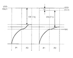
プリチャージ部(44)は、ゲート・ライン(GL)にスキャン・パルスが供給される期間毎に、データ供給部(42)がデータ信号(ID)を供給する前に2段階のプリチャージ方法で各画素(PE)のストレージキャパシタ(Cst)を所望の駆動電圧にプリチャージする。 The precharge unit (44) is a two-stage precharge method before the data supply unit (42) supplies the data signal (ID) every time the scan pulse is supplied to the gate line (GL). The storage capacitor (Cst) of each pixel (PE) is precharged to a desired drive voltage.
例えば、プリチャージ部(44)は、図5に示されるように、k番目のゲート・ライン(GLk)に低電圧のスキャン・パルスが供給される期間において、データ供給部(42)がデータ信号(IDk)を供給する前に、第1及び第2プリチャージ段階(P1,P2)を経てk番目の水平ラインのストレージキャパシタ(Cst)をプリチャージする。次に、k+1番目のゲート・ライン(GLk+1)にスキャン・パルスが供給される期間においても、データ信号(IDK+1)を供給する前に、第1及び第2プリチャージ段階(P1、P2)を経てk+1番目の水平ラインのストレージキャパシタ(Cst)をプリチャージする。 For example, as shown in FIG. 5, in the precharge unit (44), the data supply unit (42) receives the data signal during a period in which a low-voltage scan pulse is supplied to the kth gate line (GLk). Before supplying (IDk), the storage capacitor Cst of the kth horizontal line is precharged through the first and second precharge stages P1 and P2. Next, even during the period in which the scan pulse is supplied to the (k + 1) th gate line (GLk + 1), the first and second precharge stages (P1, P2) are performed before the data signal (IDK + 1) is supplied. The storage capacitor (Cst) of the (k + 1) th horizontal line is precharged.
具体的には、プリチャージ部(44)は、第1プリチャージ段階(P1)においてプリチャージ電圧(Vpc)を使用し、第2プリチャージ段階(P2)においてデータ・ライン(DL)をフローティングさせる方法を利用する。このために、プリチャージ部(44)は、第1制御信号(LOAD)に応答してプリチャージ期間の間にデータ供給部(42)とデータ・ライン(DL)との間を開放する(接続を解除する)ための第1スイッチ(SW1)と、第2制御信号(PCE)に応答してプリチャージ電圧(Vpc)をデータ・ライン(DL)に供給するための第2スイッチ(SW2)とを具備する。 Specifically, the precharge unit (44) uses the precharge voltage (Vpc) in the first precharge stage (P1) and floats the data line (DL) in the second precharge stage (P2). Use the method. For this purpose, the precharge unit (44) opens the connection between the data supply unit (42) and the data line (DL) during the precharge period in response to the first control signal (LOAD). And a second switch (SW2) for supplying a precharge voltage (Vpc) to the data line (DL) in response to the second control signal (PCE). It comprises.
第1スイッチ(SW1)は、図5のように、ゲート・ライン(GLk、GLk+1)のそれぞれにスキャン・パルスが供給される期間において、第1制御信号(LOAD)がロー(低)状態になるプリチャージ期間(P1)の間にデータ供給部(42)とデータ・ライン(DL)との間を開放する(接続を解除する)。 As shown in FIG. 5, in the first switch (SW1), the first control signal (LOAD) is in a low (low) state during a period in which the scan pulse is supplied to each of the gate lines (GLk, GLk + 1). During the precharge period (P1), the data supply unit (42) and the data line (DL) are opened (disconnected).
第2スイッチ(SW2)は、図5のように、プリチャージ期間(P1)中の第2制御信号(PCE)がハイ(高)状態になる第1プリチャージ段階(P1)において、一定のプリチャージ電圧(Vpc)をデータ・ライン(DL)に供給する。これにより、データ・ライン(DL)と、スキャン・パルスが供給されたゲート・ライン(GLk、GLk+1)と接続された画素(PE)の各々のストレージキャパシタ(Cst)をプリチャージする。この際、ストレージキャパシタ(Cst)は、電源(VDD)とプリチャージ電圧(Vpc)との差電圧(VDD−Vpc)をプリチャージするようになる。ここで、プリチャージ電圧(Vpc)は、電源(VDD)ラインの電圧降下を補償するために、最終的にプリチャージしようとする目標電圧より低く設定する。 As shown in FIG. 5, the second switch (SW2) has a constant pre-charge in the first precharge stage (P1) when the second control signal (PCE) in the precharge period (P1) is in the high (high) state. A charge voltage (Vpc) is supplied to the data line (DL). As a result, the storage capacitors (Cst) of the pixels (PE) connected to the data lines (DL) and the gate lines (GLk, GLk + 1) supplied with the scan pulse are precharged. At this time, the storage capacitor (Cst) precharges the difference voltage (VDD−Vpc) between the power supply (VDD) and the precharge voltage (Vpc). Here, the precharge voltage (Vpc) is set lower than the target voltage to be finally precharged in order to compensate for the voltage drop of the power supply (VDD) line.
次に、第2プリチャージ期間(P2)において、第1及び第2スイッチ(SW1、SW2)は、第1及び第2制御信号(LOAD、PCE)のそれぞれによりターン・オフされるので、データ・ライン(DL)はフローティング状態になる。これにより、該当する画素(PE)においてストレージキャパシタ(Cst)に充電された電圧(VDD−Vpc)が第1TFT(T1)を通じて電源(VDD)ライン側に放電される。この結果、最終的にストレージキャパシタ(Cst)にプリチャージされた電圧は各画素(PE)での電源(VDD)と第1TFT(T1)のしきい値電圧(Vth)との差電圧(VDD−Vth)になる。この際、画素(PE)の位置に従って、電源(VDD)ラインの電圧の降下があっても、ストレージキャパシタ(Cst)の各々は各画素(PE)に供給された電圧(VDD)を基準として第1TFT(T1)のしきい値電圧(Vth)だけ低い電圧をプリチャージするようになるので、電源(VDD)の電圧降下を補償することができるようになる。重ねて言えば、各画素(PE)の位置、即ち電源(VDD)ラインの電圧降下とは無関係に、ストレージキャパシタ(Cst)は一定の電圧をプリチャージすることができるようになる。 Next, in the second precharge period (P2), the first and second switches (SW1, SW2) are turned off by the first and second control signals (LOAD, PCE), respectively. The line (DL) is in a floating state. Accordingly, the voltage (VDD−Vpc) charged in the storage capacitor (Cst) in the corresponding pixel (PE) is discharged to the power supply (VDD) line side through the first TFT (T1). As a result, the voltage finally precharged in the storage capacitor (Cst) is the difference voltage (VDD−) between the power supply (VDD) in each pixel (PE) and the threshold voltage (Vth) of the first TFT (T1). Vth). At this time, even if there is a voltage drop in the power supply (VDD) line according to the position of the pixel (PE), each of the storage capacitors (Cst) has the first voltage (VDD) supplied to each pixel (PE) as a reference. Since the voltage lower by the threshold voltage (Vth) of 1 TFT (T1) is precharged, the voltage drop of the power supply (VDD) can be compensated. In other words, the storage capacitor (Cst) can precharge a constant voltage regardless of the position of each pixel (PE), that is, the voltage drop of the power supply (VDD) line.
例えば、図6に示されるように、第1ゲート・ライン(GL1)と接続された画素(PE)の各々のストレージキャパシタ(Cst)は、前述した第1及び第2プリチャージ段階(P1,P2)を経て、電圧降下のほとんどない電源(VDD)と第1TFT(T1)のしきい値電圧(Vth)との差電圧(VDD−Vth)をプリチャージするようになる。そして、第nゲート・ライン(GLn)と接続された画素(PE)の各々のストレージキャパシタ(Cst)は、前述した第1及び第2プリチャージ段階(P1,P2)を経て、電圧降下のある電圧(VDD−Vf)と第1TFT(T1)のしきい値電圧(Vth)との差電圧{(VDD−Vf)−Vth)}をプリチャージするようになる。これにより、第1ゲート・ライン(GL1)と接続された画素(PE)のストレージキャパシタ(Cst)と、第nゲート・ライン(GLn)と接続された画素(PE)のストレージキャパシタ(Cst)は、電源(VDD)ラインの電圧降下とは関係なしに、各画素(PE)に供給された電源(VDD)を基準として第1TFT(T1)のしきい値電圧(Vth)だけ低い電圧をプリチャージするようになるので、電源(VDD)の電圧降下を補償することができるようになる。 For example, as shown in FIG. 6, each storage capacitor Cst of the pixel PE connected to the first gate line GL1 includes the first and second precharge stages P1 and P2 described above. ), The voltage difference (VDD−Vth) between the power supply (VDD) having almost no voltage drop and the threshold voltage (Vth) of the first TFT (T1) is precharged. The storage capacitors Cst of the pixels PE connected to the nth gate line GLn have a voltage drop through the first and second precharge stages P1 and P2. A difference voltage {(VDD−Vf) −Vth)} between the voltage (VDD−Vf) and the threshold voltage (Vth) of the first TFT (T1) is precharged. Accordingly, the storage capacitor (Cst) of the pixel (PE) connected to the first gate line (GL1) and the storage capacitor (Cst) of the pixel (PE) connected to the nth gate line (GLn) are Regardless of the voltage drop of the power supply (VDD) line, a voltage lower by the threshold voltage (Vth) of the first TFT (T1) is precharged with reference to the power supply (VDD) supplied to each pixel (PE). As a result, the voltage drop of the power supply (VDD) can be compensated.
そして、図6のように、第1プリチャージ期間(P1)においてプリチャージ電圧(Vpc)を利用して最終プリチャージ電圧値近づけるようにストレージキャパシタ(Cst)をプリチャージするようになるので、第2プリチャージ期間(P2)において、フローティング方法により、データ・ライン(DL)上の電荷を与えられた期間(P2)内に十分に放電させることができるようになる。ここで、プリチャージ電圧(Vpc)は、電源(VDD)ラインの電圧降下を補償するために、最終的にプリチャージしようとする目標電圧、即ちVDD−Vf−Vthより低く設定する。 Then, as shown in FIG. 6, the storage capacitor (Cst) is precharged so as to approach the final precharge voltage value by using the precharge voltage (Vpc) in the first precharge period (P1). In the 2 precharge period (P2), the charge on the data line (DL) can be sufficiently discharged within the given period (P2) by the floating method. Here, the precharge voltage (Vpc) is set lower than the target voltage to be finally precharged, that is, VDD−Vf−Vth, in order to compensate for the voltage drop of the power supply (VDD) line.
この際、充分な放電のために、プリチャージ電圧(Vpc)を利用する第1プリチャージ期間(P1)より、フローティング方法を利用する第2プリチャージ期間(P2)を更に長く設定するようにする。 At this time, for sufficient discharge, the second precharge period (P2) using the floating method is set to be longer than the first precharge period (P1) using the precharge voltage (Vpc). .
上述のように、本発明によるEL表示パネルのプリチャージ方法及び装置は、プリチャージ電圧及びフローティング方法を利用することにより、電源ラインの電圧降下と関係なしに一定の電圧をプリチャージすることができる。 As described above, the EL display panel precharge method and apparatus according to the present invention can precharge a constant voltage regardless of the voltage drop of the power supply line by using the precharge voltage and the floating method. .
また、本発明によるEL表示パネルのプリチャージ方法及び装置は、フローティング方法を利用する前にプリチャージ電圧を最終プリチャージ電圧値に近づけることで、与えられた期間内に充分に放電させ、最終プリチャージ電圧値に到達することができるようになる。 In addition, the EL display panel precharge method and apparatus according to the present invention allows the precharge voltage to be close to the final precharge voltage value before using the floating method, thereby allowing sufficient discharge within a given period. The charge voltage value can be reached.
以上説明した内容を通じて、当業者であれば、本発明の技術思想を逸脱しない範囲で多様な変更及び修正が可能であることがわかる。従って、本発明の技術的範囲は、本明細書中に記載した実施例には限定されないことに留意されたい。 From the contents described above, it will be understood by those skilled in the art that various changes and modifications can be made without departing from the technical idea of the present invention. Therefore, it should be noted that the technical scope of the present invention is not limited to the embodiments described herein.
40:データ・ドライバ
42:データ供給部
44:プリチャージ部
50:画素マトリックス
54:セル駆動部
40: Data driver 42: Data supply unit 44: Precharge unit 50: Pixel matrix 54: Cell drive unit
Claims (18)
前記セル駆動部のストレージキャパシタを、第1プリチャージ電圧源を利用して第1プリチャージ電圧へとプリチャージングした後、データ信号が印加される前のプリチャージ期間に前記データ・ラインをフローティングして前記ストレージキャパシタの第1プリチャージ電圧の放電により第2プリチャージ電圧に到達させる、プリチャージ部を具備することを特徴とするELパネルのプリチャージ装置。 An electroluminescence (EL) panel precharge device, wherein the EL panel includes a plurality of pixels arranged in a matrix in a pixel region defined by an intersection between a gate line and a data line A plurality of pixels connected to the first voltage source, the gate line and the data line and having a cell driver connected between the second voltage source and the EL cell, the precharge device comprising: ,
After the storage capacitor of the cell driver is precharged to a first precharge voltage using a first precharge voltage source, the data line is floated in a precharge period before a data signal is applied. An EL panel precharge apparatus comprising: a precharge unit configured to reach a second precharge voltage by discharging the first precharge voltage of the storage capacitor.
第2プリチャージ期間の間に、前記ストレージ・キャパシタの前記第1プリチャージ電圧の放電により第2プリチャージ電圧に到達するデータ・ラインをフローティングさせる段階とを含むことを特徴とするELパネルのプリチャージ方法。 During the first precharge period, the storage capacitor of the pixel connected to the intersection between the gate line and the data line of the EL panel is precharged to the precharge voltage using a precharge voltage source. Stages,
And a step of floating a data line that reaches a second precharge voltage by discharging the first precharge voltage of the storage capacitor during a second precharge period. Charge method.
複数の画素領域を規定するように交差される複数のデータ・ライン及び複数のゲート・ラインと、
第1電圧源とセル駆動部とに接続された、各画素領域内のELセルとを具備し、
前記セル駆動部は、
前記ゲート・ライン及び前記データ・ラインに接続されると共に第2電圧源と前記ELセルとの間に接続された第1及び第2薄膜トランジスタであって、前記第2電圧源と前記ELセルとの間に電流ミラーを形成し、第2供給電圧ラインと自身のゲート電極との間に接続された前記ストレージキャパシタを有する、第1及び第2薄膜トランジスタ、
前記データ・ラインと前記第1薄膜トランジスタとの間に接続されて前記ゲート・ラインにより制御される第3薄膜トランジスタ、及び
前記第3薄膜トランジスタと前記ストレージキャパシタとの間に接続されて前記ゲート・ラインにより制御される第4薄膜トランジスタとを具備することを特徴とする請求項8記載のELパネルのプリチャージ方法。 The EL panel is
A plurality of data lines and a plurality of gate lines intersected to define a plurality of pixel regions;
An EL cell in each pixel region connected to the first voltage source and the cell driver,
The cell driver is
First and second thin film transistors connected to the gate line and the data line and connected between a second voltage source and the EL cell, wherein the second voltage source and the EL cell First and second thin film transistors having the storage capacitor connected between a second supply voltage line and its gate electrode, forming a current mirror therebetween
A third thin film transistor connected between the data line and the first thin film transistor and controlled by the gate line; and a third thin film transistor connected between the third thin film transistor and the storage capacitor and controlled by the gate line 9. The method of precharging an EL panel according to claim 8, further comprising a fourth thin film transistor.
前記第2供給電圧は、電圧降下(Vf)を含む前記第2供給電圧ラインを経由して前記第2電圧源から印加されることを特徴とする請求項10記載のELパネルのプリチャージ方法。 The precharge voltage is lower than a difference voltage (VDD−Vf−Vth) between a second supply voltage (VDD−Vf) supplied to each pixel and a threshold voltage (Vth) of the first thin film transistor. And further comprising a setting step,
11. The method of claim 10, wherein the second supply voltage is applied from the second voltage source via the second supply voltage line including a voltage drop (Vf).
The method of claim 17, wherein the second precharge period is longer than the first precharge period.
Applications Claiming Priority (1)
| Application Number | Priority Date | Filing Date | Title |
|---|---|---|---|
| KR1020040022123A KR101076424B1 (en) | 2004-03-31 | 2004-03-31 | Method and apparatus for precharging electro luminescence panel |
Publications (2)
| Publication Number | Publication Date |
|---|---|
| JP2005292783A true JP2005292783A (en) | 2005-10-20 |
| JP4303193B2 JP4303193B2 (en) | 2009-07-29 |
Family
ID=35049952
Family Applications (1)
| Application Number | Title | Priority Date | Filing Date |
|---|---|---|---|
| JP2004373599A Expired - Lifetime JP4303193B2 (en) | 2004-03-31 | 2004-12-24 | Method and apparatus for precharging an electroluminescence panel |
Country Status (4)
| Country | Link |
|---|---|
| US (1) | US7492336B2 (en) |
| JP (1) | JP4303193B2 (en) |
| KR (1) | KR101076424B1 (en) |
| CN (1) | CN100433102C (en) |
Cited By (1)
| Publication number | Priority date | Publication date | Assignee | Title |
|---|---|---|---|---|
| JP2021164403A (en) * | 2020-03-31 | 2021-10-11 | アナパス インコーポレーテッドAnapass Inc. | Display device and method of calibrating driving time of boost circuit |
Families Citing this family (31)
| Publication number | Priority date | Publication date | Assignee | Title |
|---|---|---|---|---|
| US7319446B2 (en) * | 2005-04-19 | 2008-01-15 | Lg.Philips Lcd Co., Ltd. | Organic electroluminescent display device and driving method thereof |
| KR100624314B1 (en) * | 2005-06-22 | 2006-09-19 | 삼성에스디아이 주식회사 | Light emitting display device and thin film transistor |
| KR101127851B1 (en) * | 2005-06-30 | 2012-03-21 | 엘지디스플레이 주식회사 | A light emitting display device and a method for driving the same |
| US20070139318A1 (en) * | 2005-12-21 | 2007-06-21 | Lg Electronics Inc. | Light emitting device and method of driving the same |
| TWI335565B (en) * | 2006-03-24 | 2011-01-01 | Himax Tech Ltd | Pixel driving method of oled display and apparatus thereof |
| TWI337451B (en) * | 2006-04-03 | 2011-02-11 | Novatek Microelectronics Corp | Method and related device of source driver with reduced power consumption |
| KR100756275B1 (en) * | 2006-04-28 | 2007-09-06 | 엘지전자 주식회사 | Light emitting device and method for driving same |
| KR100736574B1 (en) * | 2006-04-28 | 2007-07-06 | 엘지전자 주식회사 | Light emitting device and method for driving same |
| KR100806817B1 (en) * | 2006-06-26 | 2008-02-25 | 엘지.필립스 엘시디 주식회사 | Driving device and driving method of organic light emitting device |
| US8107032B2 (en) * | 2006-11-02 | 2012-01-31 | Sharp Kabushiki Kaisha | Active matrix substrate and display device having the same |
| US7920110B2 (en) * | 2007-03-28 | 2011-04-05 | Himax Technologies Limited | Pixel circuit |
| JP5467484B2 (en) * | 2007-06-29 | 2014-04-09 | カシオ計算機株式会社 | Display drive device, drive control method thereof, and display device including the same |
| JP4715840B2 (en) * | 2007-12-14 | 2011-07-06 | エプソンイメージングデバイス株式会社 | Drive device, electro-optical device, and electronic apparatus |
| KR100911980B1 (en) * | 2008-03-28 | 2009-08-13 | 삼성모바일디스플레이주식회사 | Pixel and organic light emitting display device using same |
| CN102047312B (en) | 2009-03-06 | 2014-09-10 | 松下电器产业株式会社 | Image display apparatus and driving method therefor |
| WO2010137268A1 (en) * | 2009-05-26 | 2010-12-02 | パナソニック株式会社 | Image display device and method for driving same |
| CN102714019B (en) * | 2010-09-06 | 2015-07-08 | 株式会社日本有机雷特显示器 | Display device and driving method thereof |
| TWI471840B (en) * | 2010-11-05 | 2015-02-01 | Wintek Corp | Driver circuit of light-emitting device |
| TWI473062B (en) * | 2013-01-22 | 2015-02-11 | Au Optronics Corp | Organic light emitting diode display device and driving method thereof |
| CN103093723A (en) * | 2013-03-04 | 2013-05-08 | 陈鑫 | Active pixel drive circuit applied to organic light emitting diodes and capable of carrying out threshold value compensation |
| JP2015031864A (en) * | 2013-08-05 | 2015-02-16 | 三星ディスプレイ株式會社Samsung Display Co.,Ltd. | Pixel circuit and driving method thereof |
| KR102269785B1 (en) * | 2014-06-17 | 2021-06-29 | 삼성디스플레이 주식회사 | Pixel circuit and organic light emitting display device having the same |
| CN104537997B (en) * | 2015-01-04 | 2017-09-22 | 京东方科技集团股份有限公司 | A kind of image element circuit and its driving method and display device |
| CN104637445B (en) * | 2015-02-03 | 2017-03-08 | 深圳市华星光电技术有限公司 | AMOLED pixel-driving circuit and image element driving method |
| KR20160148831A (en) * | 2015-06-16 | 2016-12-27 | 삼성디스플레이 주식회사 | Display device and driving method thereof |
| CN107068058B (en) * | 2017-04-28 | 2019-12-03 | 深圳市华星光电技术有限公司 | Pixel-driving circuit, display panel and image element driving method |
| KR102651754B1 (en) * | 2018-10-12 | 2024-03-29 | 삼성디스플레이 주식회사 | Display device and driving method of the display device |
| CN113506538B (en) * | 2021-07-16 | 2022-10-04 | 深圳市华星光电半导体显示技术有限公司 | Pixel driving circuit and display panel |
| CN114974084B (en) * | 2022-05-12 | 2023-09-26 | 惠科股份有限公司 | Driving circuit and method of display unit and display device |
| CN115171607B (en) * | 2022-09-06 | 2023-01-31 | 惠科股份有限公司 | Pixel circuit, display panel and display device |
| CN115631726B (en) * | 2022-12-21 | 2023-03-10 | 惠科股份有限公司 | Array substrate and display panel |
Family Cites Families (9)
| Publication number | Priority date | Publication date | Assignee | Title |
|---|---|---|---|---|
| JPH06337400A (en) * | 1993-05-31 | 1994-12-06 | Sharp Corp | Matrix-type display device and driving method |
| TW530287B (en) * | 1998-09-03 | 2003-05-01 | Samsung Electronics Co Ltd | Display device, and apparatus and method for driving display device |
| GB0008019D0 (en) * | 2000-03-31 | 2000-05-17 | Koninkl Philips Electronics Nv | Display device having current-addressed pixels |
| JP2002244617A (en) * | 2001-02-15 | 2002-08-30 | Sanyo Electric Co Ltd | Organic el pixel circuit |
| US7079130B2 (en) * | 2001-05-09 | 2006-07-18 | Clare Micronix Integrated Systems, Inc. | Method for periodic element voltage sensing to control precharge |
| KR100819138B1 (en) * | 2001-08-25 | 2008-04-21 | 엘지.필립스 엘시디 주식회사 | Driving device of electroluminescence panel and driving method thereof |
| KR100433216B1 (en) * | 2001-11-06 | 2004-05-27 | 엘지.필립스 엘시디 주식회사 | Apparatus and method of driving electro luminescence panel |
| JP3627710B2 (en) * | 2002-02-14 | 2005-03-09 | セイコーエプソン株式会社 | Display drive circuit, display panel, display device, and display drive method |
| AU2003278447A1 (en) * | 2002-11-15 | 2004-06-15 | Koninklijke Philips Electronics N.V. | Display device with pre-charging arrangement |
-
2004
- 2004-03-31 KR KR1020040022123A patent/KR101076424B1/en not_active Expired - Lifetime
- 2004-08-04 CN CNB2004100701703A patent/CN100433102C/en not_active Expired - Lifetime
- 2004-12-24 JP JP2004373599A patent/JP4303193B2/en not_active Expired - Lifetime
- 2004-12-28 US US11/022,689 patent/US7492336B2/en active Active
Cited By (2)
| Publication number | Priority date | Publication date | Assignee | Title |
|---|---|---|---|---|
| JP2021164403A (en) * | 2020-03-31 | 2021-10-11 | アナパス インコーポレーテッドAnapass Inc. | Display device and method of calibrating driving time of boost circuit |
| JP7098194B2 (en) | 2020-03-31 | 2022-07-11 | アナパス インコーポレーテッド | Calibration method of drive time of display device and voltage supply circuit |
Also Published As
| Publication number | Publication date |
|---|---|
| CN100433102C (en) | 2008-11-12 |
| US20050219166A1 (en) | 2005-10-06 |
| KR20050096671A (en) | 2005-10-06 |
| US7492336B2 (en) | 2009-02-17 |
| KR101076424B1 (en) | 2011-10-25 |
| CN1677465A (en) | 2005-10-05 |
| JP4303193B2 (en) | 2009-07-29 |
Similar Documents
| Publication | Publication Date | Title |
|---|---|---|
| JP4303193B2 (en) | Method and apparatus for precharging an electroluminescence panel | |
| US8120553B2 (en) | Organic light emitting diode display device | |
| US6724151B2 (en) | Apparatus and method of driving electro luminescence panel | |
| US7106281B2 (en) | Apparatus and method for driving electro-luminescence panel | |
| JP5080733B2 (en) | Display device and driving method thereof | |
| KR100476368B1 (en) | Data driving apparatus and method of organic electro-luminescence display panel | |
| CN100570689C (en) | Organic light emitting diode display device and driving method thereof | |
| KR101042956B1 (en) | Pixel circuit and organic light emitting display device using the same | |
| US6693383B2 (en) | Electro-luminescence panel | |
| EP1473689A2 (en) | Pixel circuit, display panel, image display device and driving method thereof | |
| CN100458898C (en) | Display panel, light-emitting display device using the display panel, and driving method thereof | |
| CN100378781C (en) | Display panel and driving method thereof | |
| KR101419244B1 (en) | Organic light emitting diode display device and driving method thereof | |
| CN100394468C (en) | Electroluminescence display and its driving method | |
| KR20050095148A (en) | Electro-luminescence display apparatus and driving method thereof | |
| EP1724748B1 (en) | Method for driving flat panel display | |
| KR20090073688A (en) | Light emitting display device and driving method thereof | |
| CN1316443C (en) | Current driven active matrix organic light emitting diode pixel circuit and driving method | |
| US8059065B2 (en) | Method and apparatus for driving electro-luminescence display panel | |
| KR100692847B1 (en) | Selective precharging method and apparatus for organic electroluminescent display panel | |
| KR100607514B1 (en) | Electro-luminescence display and its driving method | |
| KR101240658B1 (en) | Display device and driving method thereof | |
| KR20050068233A (en) | Electro-luminescence panel | |
| KR20050064299A (en) | Electro-luminescence display apparatus and driving method thereof |
Legal Events
| Date | Code | Title | Description |
|---|---|---|---|
| A977 | Report on retrieval |
Free format text: JAPANESE INTERMEDIATE CODE: A971007 Effective date: 20080616 |
|
| A131 | Notification of reasons for refusal |
Free format text: JAPANESE INTERMEDIATE CODE: A131 Effective date: 20080702 |
|
| A601 | Written request for extension of time |
Free format text: JAPANESE INTERMEDIATE CODE: A601 Effective date: 20081002 |
|
| A602 | Written permission of extension of time |
Free format text: JAPANESE INTERMEDIATE CODE: A602 Effective date: 20081007 |
|
| A521 | Request for written amendment filed |
Free format text: JAPANESE INTERMEDIATE CODE: A523 Effective date: 20081031 |
|
| A131 | Notification of reasons for refusal |
Free format text: JAPANESE INTERMEDIATE CODE: A131 Effective date: 20081201 |
|
| A521 | Request for written amendment filed |
Free format text: JAPANESE INTERMEDIATE CODE: A523 Effective date: 20090227 |
|
| TRDD | Decision of grant or rejection written | ||
| A01 | Written decision to grant a patent or to grant a registration (utility model) |
Free format text: JAPANESE INTERMEDIATE CODE: A01 Effective date: 20090330 |
|
| A01 | Written decision to grant a patent or to grant a registration (utility model) |
Free format text: JAPANESE INTERMEDIATE CODE: A01 |
|
| A61 | First payment of annual fees (during grant procedure) |
Free format text: JAPANESE INTERMEDIATE CODE: A61 Effective date: 20090423 |
|
| FPAY | Renewal fee payment (event date is renewal date of database) |
Free format text: PAYMENT UNTIL: 20120501 Year of fee payment: 3 |
|
| R150 | Certificate of patent or registration of utility model |
Ref document number: 4303193 Country of ref document: JP Free format text: JAPANESE INTERMEDIATE CODE: R150 Free format text: JAPANESE INTERMEDIATE CODE: R150 |
|
| FPAY | Renewal fee payment (event date is renewal date of database) |
Free format text: PAYMENT UNTIL: 20130501 Year of fee payment: 4 |
|
| R250 | Receipt of annual fees |
Free format text: JAPANESE INTERMEDIATE CODE: R250 |
|
| R250 | Receipt of annual fees |
Free format text: JAPANESE INTERMEDIATE CODE: R250 |
|
| R250 | Receipt of annual fees |
Free format text: JAPANESE INTERMEDIATE CODE: R250 |
|
| R250 | Receipt of annual fees |
Free format text: JAPANESE INTERMEDIATE CODE: R250 |
|
| R250 | Receipt of annual fees |
Free format text: JAPANESE INTERMEDIATE CODE: R250 |
|
| R250 | Receipt of annual fees |
Free format text: JAPANESE INTERMEDIATE CODE: R250 |
|
| R250 | Receipt of annual fees |
Free format text: JAPANESE INTERMEDIATE CODE: R250 |
|
| R250 | Receipt of annual fees |
Free format text: JAPANESE INTERMEDIATE CODE: R250 |
|
| R250 | Receipt of annual fees |
Free format text: JAPANESE INTERMEDIATE CODE: R250 |
|
| R250 | Receipt of annual fees |
Free format text: JAPANESE INTERMEDIATE CODE: R250 |
|
| R250 | Receipt of annual fees |
Free format text: JAPANESE INTERMEDIATE CODE: R250 |
|
| R250 | Receipt of annual fees |
Free format text: JAPANESE INTERMEDIATE CODE: R250 |
|
| R250 | Receipt of annual fees |
Free format text: JAPANESE INTERMEDIATE CODE: R250 |
|
| EXPY | Cancellation because of completion of term |