JP2005292738A - Optical module - Google Patents

Optical module Download PDF

Info

Publication number
JP2005292738A
JP2005292738A JP2004111686A JP2004111686A JP2005292738A JP 2005292738 A JP2005292738 A JP 2005292738A JP 2004111686 A JP2004111686 A JP 2004111686A JP 2004111686 A JP2004111686 A JP 2004111686A JP 2005292738 A JP2005292738 A JP 2005292738A
Authority
JP
Japan
Prior art keywords
guide pin
transparent substrate
fitting hole
optical
optical element
Prior art date
Legal status (The legal status is an assumption and is not a legal conclusion. Google has not performed a legal analysis and makes no representation as to the accuracy of the status listed.)
Pending
Application number
JP2004111686A
Other languages
Japanese (ja)
Inventor
Kenji Kogo
健治 古後
Takuma Saka
卓磨 坂
Masato Shishikura
正人 宍倉
Current Assignee (The listed assignees may be inaccurate. Google has not performed a legal analysis and makes no representation or warranty as to the accuracy of the list.)
Hitachi Ltd
Original Assignee
Hitachi Ltd
Priority date (The priority date is an assumption and is not a legal conclusion. Google has not performed a legal analysis and makes no representation as to the accuracy of the date listed.)
Filing date
Publication date
Application filed by Hitachi Ltd filed Critical Hitachi Ltd
Priority to JP2004111686A priority Critical patent/JP2005292738A/en
Publication of JP2005292738A publication Critical patent/JP2005292738A/en
Pending legal-status Critical Current

Links

Images

Landscapes

  • Optical Couplings Of Light Guides (AREA)

Abstract

【課題】従来、ガイドピンを用いた光結合構造では、気密構造とするためにファイバの調芯作業が必要であり生産性が悪くコスト低減の問題となっていた。
【解決手段】素子、透明基板、ファイバ等の全て光学部品をガイドピンと嵌合する嵌合穴および同様機能を持つ基板等を用いて、ガイドピン基準として位置合わせ行う。そのため、各部品をガイドピンに挿入するだけで良好な光結合構造が得られる。さらに、ガイドピン、光素子を囲むように封止リングを設け、封止リング開口部を透明基板で封止する。さらに、この時生じる透明基板の嵌合穴とガイドピンの隙間を封止材で埋めて封止リング内を気密とする。
【選択図】図1
Conventionally, in an optical coupling structure using a guide pin, fiber alignment is required to achieve an airtight structure, resulting in poor productivity and cost reduction.
Alignment is performed using a fitting hole for fitting all optical components such as an element, a transparent substrate, and a fiber with a guide pin and a substrate having the same function as a guide pin reference. Therefore, a good optical coupling structure can be obtained simply by inserting each component into the guide pin. Further, a sealing ring is provided so as to surround the guide pin and the optical element, and the sealing ring opening is sealed with a transparent substrate. Further, the gap between the fitting hole of the transparent substrate and the guide pin generated at this time is filled with a sealing material to make the inside of the sealing ring airtight.
[Selection] Figure 1

Description

この発明は、光モジュールに関し、特に気密封止方法および製造方法に関し、さらにはガイドピンを用いて光素子とファイバの相対位置合わせを行う光モジュールの光結合構造に関する。   The present invention relates to an optical module, and more particularly to an airtight sealing method and a manufacturing method, and further to an optical coupling structure of an optical module that performs relative alignment between an optical element and a fiber using a guide pin.

近年、画像や映像の高画質・高解像度化が進んでおり通信データが大容量化している。そのため通信速度の高速化が求められ、現在の光通信では幹線系、メトロ系においては10Gbpsを超える速度での通信が行われている。この時、同一ビル内や局内といったデータの集中する伝送装置間の通信には10Gbpsを超える速度での通信が必要となる。一般にノード内伝送装置間の通信は近距離であるためファイバ長によるコストの差があまり生じない。そのため伝送装置間の通信では1チャンネルで40Gbpsを超える速度の高価なモジュールよりは、1チャンネル速度が数Mbps―数Gbps程度の安価な多チャンネル光モジュールが用いられている。今後はさらに通信容量の大容量化が進むことが予測されることから、1チャンネル伝送速度を10Gbpsとした多チャンネルの光モジュールが求められてくる。   In recent years, high-quality and high-resolution images and videos have progressed, and communication data has increased in capacity. Therefore, an increase in communication speed is required, and in current optical communication, communication at a speed exceeding 10 Gbps is performed in the trunk line system and the metro system. At this time, communication at a speed exceeding 10 Gbps is required for communication between transmission apparatuses in which data is concentrated, such as in the same building or station. In general, since communication between intra-node transmission apparatuses is a short distance, there is little difference in cost due to fiber length. Therefore, in communication between transmission apparatuses, an inexpensive multi-channel optical module having a channel speed of several Mbps to several Gbps is used rather than an expensive module having a speed exceeding 40 Gbps in one channel. Since it is predicted that the communication capacity will further increase in the future, a multi-channel optical module with a single channel transmission speed of 10 Gbps is required.

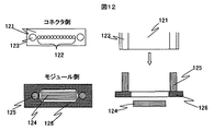
一般的に多チャンネル光モジュールでは、MTコネクタを用いて光結合を行なう。図12にMTコネクタの構造を示す。MT型コネクタ121の端面にはファイバアレイ122が配置されており、そのファイバアレイ122の両側には嵌合穴123が設けられている。この嵌合穴123はファイバアレイ122に対して高精度で位置決めされており、光素子124側に設けているガイドピン125に前記嵌合穴を挿入して、ファイバアレイ122と光素子124との位置関係が決まり光結合を行う。そのため、コネクタ側においては、嵌合穴123とファイバアレイ122、モジュール側においてはガイドピン125と光素子124の相対位置精度が重要となる。   In general, in a multi-channel optical module, optical coupling is performed using an MT connector. FIG. 12 shows the structure of the MT connector. A fiber array 122 is disposed on the end face of the MT connector 121, and fitting holes 123 are provided on both sides of the fiber array 122. The fitting hole 123 is positioned with high accuracy with respect to the fiber array 122, and the fitting hole is inserted into a guide pin 125 provided on the optical element 124 side to connect the fiber array 122 and the optical element 124. The positional relationship is determined and optical coupling is performed. Therefore, the relative positional accuracy of the fitting hole 123 and the fiber array 122 is important on the connector side, and the guide pin 125 and the optical element 124 are important on the module side.

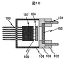
ここで、従来広く用いられているMTコネクタと結合する多チャンネルモジュールの光構造を図10に示す。本構造ではガイドピン101をパッケージ106内に挿入せず、ガイドピン101と光素子104との位置合わせは光素子104を実際に発光または受光させて行っている。作製手順は、まず、光素子104をパッケージ106内の所定の位置に実装し、光素子104と集積回路107、配線パターン109をワイヤ108で接続する。また、別の場所でパッケージ106開口部を塞ぐリッドをガイドピン101とレンズアレイ105をフランジ102、103で組合せて作製する。実際に光素子104を駆動させファイバの出力をモニタして最適な位置に調芯し、作製したリッドをパッケージ106に固定する。   Here, FIG. 10 shows an optical structure of a multi-channel module coupled with an MT connector that has been widely used conventionally. In this structure, the guide pin 101 is not inserted into the package 106, and the alignment between the guide pin 101 and the optical element 104 is performed by causing the optical element 104 to actually emit or receive light. In the manufacturing procedure, first, the optical element 104 is mounted at a predetermined position in the package 106, and the optical element 104, the integrated circuit 107, and the wiring pattern 109 are connected by the wire 108. Further, a lid for closing the opening of the package 106 at another location is manufactured by combining the guide pins 101 and the lens array 105 with the flanges 102 and 103. The optical element 104 is actually driven, the output of the fiber is monitored and the fiber is aligned at an optimum position, and the manufactured lid is fixed to the package 106.

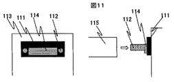
また、他の光結合構造を図11に示す。ガイドピン112の間隔を精密に制御して台座113に固定する。そのガイドピン112に、光素子114が搭載されガイドピン112と嵌合する穴を有する素子基板111を挿入する。この光素子114は素子基板111の嵌合穴と相対位置精度良く素子基板111に搭載されている。光結合はガイドピン112にMTコネクタ115の嵌合穴を挿入して行っている。   Another optical coupling structure is shown in FIG. The distance between the guide pins 112 is precisely controlled and fixed to the pedestal 113. The element substrate 111 having a hole in which the optical element 114 is mounted and fitted with the guide pin 112 is inserted into the guide pin 112. The optical element 114 is mounted on the element substrate 111 with a relative positional accuracy with respect to the fitting hole of the element substrate 111. Optical coupling is performed by inserting a fitting hole of the MT connector 115 into the guide pin 112.

特開1997−243867号公報JP 1997-243867 A

図10に示す構造では、気密構造であるため信頼性が高い。しかし、組立工程に調芯作業があり複雑なため生産性が悪くコスト・時間の増加に繋がっていた。さらに、モジュールの高速化が進むに伴い実装トレランスが狭くなり調芯作業は難しくなっている。   The structure shown in FIG. 10 is highly reliable because it is an airtight structure. However, since the assembling process is centered and complicated, the productivity is poor and the cost and time are increased. Furthermore, as the speed of modules increases, mounting tolerances become narrower and alignment work becomes difficult.

また、図11に示す構造では、組立は全てガイドピンを基準にしてガイドピンに部品を挿入して作製していくため組立が簡単で生産性が良い。しかし、気密構造でないためモジュール使用環境の影響を大きく受けてしまい光素子の劣化を早める等、信頼性に問題がある。
そこで、本発明は気密封止として信頼性を保ったまま、調芯作業不要で組立が簡単で生産性の良い光モジュールの光結合構造を提供する。
Further, in the structure shown in FIG. 11, all assembly is performed by inserting parts into the guide pins with reference to the guide pins, so that the assembly is simple and the productivity is good. However, since it is not an airtight structure, there is a problem in reliability, such as being greatly affected by the environment in which the module is used and deteriorating the optical element.
Therefore, the present invention provides an optical coupling structure of an optical module that is easy to assemble and has good productivity while maintaining reliability as an airtight seal.

本発明において上記課題を解決するための構造を図1に示す。光素子13、透明基板12、ファイバを全てガイドピン11基準として位置合わせを行い作製する。気密封止には封止リング14をガイドピン11と光素子13を囲むように設け、封止リング14開口部を透明基板12で塞ぎ、さらに透明基板12の嵌合穴とガイドピン11との隙間を封止材16で埋める。
さらに本発明では前記封止材16に半田を用いた。半田はメタライズしていない箇所には濡れないので、透明基板12嵌合穴および嵌合穴周辺とガイドピン11にメタライズした。
A structure for solving the above problems in the present invention is shown in FIG. The optical element 13, the transparent substrate 12, and the fiber are all aligned with respect to the guide pin 11 and manufactured. For hermetic sealing, a sealing ring 14 is provided so as to surround the guide pin 11 and the optical element 13, the opening of the sealing ring 14 is closed with the transparent substrate 12, and the fitting hole of the transparent substrate 12 and the guide pin 11 are closed. The gap is filled with the sealing material 16.
Further, in the present invention, solder is used for the sealing material 16. Since the solder does not get wet in the portions that are not metallized, the transparent substrate 12 fitting holes, the fitting hole periphery, and the guide pins 11 were metalized.

光結合効率を考えるとレンズ等の集光部品を用いずに結合を行う場合は透明基板とコネクタを出来る限り近接して配置する必要がある。そのため、半田の盛上りが近接配置の障害となるため、半田の盛上りを防止する必要がある。そこで、嵌合穴のメタライズを透明基板のコネクタ側の面には形成せずに穴側面と素子側の面のみに形成する。さらには、嵌合穴を2段構造とし素子側の段のみにメタライズを施し透明基板表面よりも上面へ半田が盛上ることを防いでいる。   Considering optical coupling efficiency, when coupling is performed without using a condensing part such as a lens, it is necessary to dispose the transparent substrate and the connector as close as possible. For this reason, since the rise of solder becomes an obstacle to the proximity arrangement, it is necessary to prevent the rise of solder. Therefore, the metallization of the fitting hole is not formed on the surface on the connector side of the transparent substrate, but only on the side surface of the hole and the surface on the element side. Furthermore, the fitting hole has a two-stage structure, and metallization is performed only on the element side to prevent the solder from rising above the transparent substrate surface.

また、半田を溶解した時に半田がガイドピンを伝わり光素子13側に流れると素子基板15等の配線を短絡させてしまい良好な特性が得られない恐れがある。また、半田がコネクタ側の流れた場合はコネクタを所定の位置に配置できない。あるいは、透明基板12とコネクタを近接位置できないと言った問題がある。そこで、半田がガイドピンを伝わり不要な箇所に流れないようにするためガイドピンに段差を形成する。また、別の方法としてガイドピンにメタライズあるいは、半田流れ防止ダムを形成しガイドピン一部に半田が固着するようにする。
さらに、前記の述べてきた構造において透明基板にレンズ機能を持たせ結合効率を改善している。また、集積回路を封止リング内に配置し光素子と集積回路を近接させ寄生インダクタンスを抑えて高周波特性を改善している。
Moreover, when the solder is melted and the solder flows through the guide pins and flows toward the optical element 13, the wiring of the element substrate 15 and the like may be short-circuited, and good characteristics may not be obtained. Further, when the solder flows on the connector side, the connector cannot be disposed at a predetermined position. Alternatively, there is a problem that the transparent substrate 12 and the connector cannot be positioned close to each other. Therefore, a step is formed in the guide pin so that the solder does not travel through the guide pin and flow to unnecessary portions. As another method, metallization or solder flow prevention dams are formed on the guide pins so that the solder is fixed to a part of the guide pins.
Further, in the structure described above, the coupling efficiency is improved by providing the transparent substrate with a lens function. In addition, the integrated circuit is disposed in the sealing ring, the optical element and the integrated circuit are brought close to each other, and parasitic inductance is suppressed to improve high frequency characteristics.

本発明を用いれば、光結合の組立を簡単行えるため生産性がよく低コスト化が図れ、さらに気密構造とできるため信頼性が向上した光モジュールが実現可能である。   By using the present invention, it is possible to simplify the assembly of the optical coupling, so that the productivity can be improved and the cost can be reduced. Further, since the airtight structure can be obtained, an optical module with improved reliability can be realized.

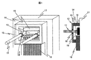
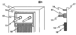
以下図面を用いて本発明の実施形態を詳細に説明する。図1は本発明によるモジュールの斜視図と断面図である。封止リング14の内側に、2本のガイドピン11、光素子13を搭載した素子基板15が配置されている。さらに、封止リング14開口部には、透明基板12を固定し、ガイドピン11と透明基板12の隙間を封止材16で埋めて封止リング内の気密を保っている。   Hereinafter, embodiments of the present invention will be described in detail with reference to the drawings. FIG. 1 is a perspective view and a sectional view of a module according to the present invention. An element substrate 15 on which the two guide pins 11 and the optical element 13 are mounted is disposed inside the sealing ring 14. Further, the transparent substrate 12 is fixed to the opening of the sealing ring 14, and the gap between the guide pin 11 and the transparent substrate 12 is filled with the sealing material 16 to keep the sealing ring airtight.

次に図2を参照して各部品の詳細な説明を行う。台座17には2本のガイドピン11と封止リング14が固定されている。このガイドピン11の間隔は精度良く固定されているが絶対位置に関しては特に精度を必要としない。また、封止リング14はガイドピン11位置を基準として台座17に溶接またはロウ付け等で固定している。さらに、封止リング14はセラミックの積層パッケージを用いて、封止リング内部と外部で電気信号の伝達を行う配線パターン18を設けている。   Next, each component will be described in detail with reference to FIG. Two guide pins 11 and a sealing ring 14 are fixed to the base 17. The distance between the guide pins 11 is fixed with high accuracy, but the accuracy is not particularly required with respect to the absolute position. Further, the sealing ring 14 is fixed to the pedestal 17 by welding or brazing or the like with respect to the position of the guide pin 11. Further, the sealing ring 14 is provided with a wiring pattern 18 for transmitting an electric signal inside and outside the sealing ring using a ceramic laminated package.

次に素子基板15について説明する。基板の表面にガイドピン11と嵌合する穴22とアライメントマーク21とAuSn半田23を設ける。前記アライメントマーク21と嵌合穴22は一回のフォトリソグラフィで形成し相対位置は<±2μmの高精度で作製する。このアライメントマーク21付近に光素子13を搭載するためのAuSn半田23を設ける。素子基板15の厚さは、配線パターン18と光素子13表面の高さが同じとなるように配線パターン18と光素子13の厚さの差としている。   Next, the element substrate 15 will be described. A hole 22 for fitting the guide pin 11, an alignment mark 21, and AuSn solder 23 are provided on the surface of the substrate. The alignment mark 21 and the fitting hole 22 are formed by a single photolithography, and the relative positions are manufactured with high accuracy of <± 2 μm. An AuSn solder 23 for mounting the optical element 13 is provided near the alignment mark 21. The thickness of the element substrate 15 is the difference in thickness between the wiring pattern 18 and the optical element 13 so that the height of the surface of the wiring pattern 18 and the optical element 13 is the same.

次に、光素子13は12チャンネルアレイの面発光素子である。表面には発光点、電極パターン、アライメントマークが形成され裏面には素子基板15のAuSn半田23と固定するためのメタライズを施している。
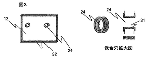
次に透明基板12について説明する。透明基板12は封止リング14の開口部を封止する役割がある。そこで、気密封止の可能な石英系のガラスを用いて作製した。透明基板12の表面にはガイドピン11と嵌合する嵌合穴24が2つあり、この嵌合穴24の間隔は精度よく作製している。
Next, the optical element 13 is a 12-channel array surface emitting element. A light emitting point, an electrode pattern, and an alignment mark are formed on the front surface, and metallization is performed on the back surface for fixing to the AuSn solder 23 of the element substrate 15.
Next, the transparent substrate 12 will be described. The transparent substrate 12 serves to seal the opening of the sealing ring 14. Therefore, it was manufactured using quartz glass that can be hermetically sealed. The surface of the transparent substrate 12 has two fitting holes 24 for fitting with the guide pins 11, and the intervals between the fitting holes 24 are made with high accuracy.

さらに図2を参照してモジュール組立手順について説明する。まず、光素子13を素子基板15に搭載する。搭載の位置合わせは光素子13と素子基板15の両方に設けているアライメントマークを用いて行う。位置合わせ後、光素子13を素子基板15のAuSn半田23上に仮固定する。その後、窒素雰囲気下でリフロし本固定する。以上の工程により、光素子13は嵌合穴22に対して高精度に実装できる。なぜなら、先に述べたように嵌合穴22とアライメントマーク21は一回のフォトリソグラフィで作製しているため相対位置は高精度に作製されており、このアライメントマーク21を用いて光素子13との位置合わせを行い搭載しているからである。   Further, the module assembly procedure will be described with reference to FIG. First, the optical element 13 is mounted on the element substrate 15. Mounting alignment is performed using alignment marks provided on both the optical element 13 and the element substrate 15. After alignment, the optical element 13 is temporarily fixed on the AuSn solder 23 of the element substrate 15. Then, reflow under a nitrogen atmosphere and fix it. Through the above steps, the optical element 13 can be mounted in the fitting hole 22 with high accuracy. This is because, as described above, the fitting hole 22 and the alignment mark 21 are produced by a single photolithography, so that the relative position is produced with high precision. This is because the positioning is carried out.

次にガイドピン11に各部品を挿入して光結合構造を作製する。まず、光素子13を搭載した素子基板15を嵌合穴22がガイドピン11と嵌合するように挿入して、台座17と接着剤で固定する。それから、封止リング14内部の配線パターン18と光素子13をワイヤ19で接続する。その後、透明基板12を嵌合穴24がガイドピン11と嵌合するように挿入して封止リング14と気密のとれる接着剤で固定する。最後にガイドピン11と透明基板嵌合穴24の隙間を封止材16で埋めて封止リング14内部に配置された光素子13を気密に保つ。   Next, each component is inserted into the guide pin 11 to produce an optical coupling structure. First, the element substrate 15 on which the optical element 13 is mounted is inserted so that the fitting hole 22 is fitted to the guide pin 11 and is fixed to the base 17 with an adhesive. Then, the wiring pattern 18 inside the sealing ring 14 and the optical element 13 are connected by a wire 19. Thereafter, the transparent substrate 12 is inserted so that the fitting hole 24 is fitted to the guide pin 11 and fixed to the sealing ring 14 with an airtight adhesive. Finally, the gap between the guide pin 11 and the transparent substrate fitting hole 24 is filled with the sealing material 16 to keep the optical element 13 disposed inside the sealing ring 14 airtight.

また、使用環境の温度変化等により透明基板を割れにくくする為に、透明基板12に封止リング14と線膨張係数の近い材質の透過セラミック等を選択するとより効果的である。また、透明基板12は一枚の基板で作製する必要がなく、光を透過する部分のみガラスや透過セラミック等の光の透過する基板を用いて光の透過しない部分には金属等を使用し前記光の透過する基板と金属を気密の保てる方法で接着して透明基板12を作製しても効果的である。さらに、ガイドピン11と嵌合穴24の隙間の封止方法は、レーザ照射等による溶接、さらには低融点ガラス等を用いた気密が保てる接着方法であれば良い。また、本構造は面発光素子の変わりに端面発光素子や受光素子を用いても効果は同じである。
以上述べた構造でモジュールを作製すれば、光素子13は気密に保たれ、組立も調芯作業が無く簡単に行うことが出来る。
Further, in order to make the transparent substrate difficult to break due to temperature changes in the usage environment, it is more effective to select a transparent ceramic or the like having a linear expansion coefficient close to that of the sealing ring 14 for the transparent substrate 12. In addition, the transparent substrate 12 does not need to be made of a single substrate, only a portion that transmits light uses a substrate that transmits light, such as glass or transmissive ceramic, and a portion that does not transmit light uses metal or the like. It is also effective to produce the transparent substrate 12 by bonding the light transmitting substrate and the metal in a manner that keeps the gas tight. Further, the method for sealing the gap between the guide pin 11 and the fitting hole 24 may be an adhesion method that can maintain the airtightness using welding by laser irradiation or the like, and further using low melting point glass or the like. In addition, this structure has the same effect even when an end face light emitting element or a light receiving element is used instead of the surface light emitting element.
If a module is manufactured with the structure described above, the optical element 13 is kept airtight, and assembly can be easily performed without alignment work.

本実施例では、図1に示す封止材16に半田を用いる。そこで、封止リング開口部を塞ぐ図2に示す透明基板12は図3に示すように嵌合穴24及び嵌合穴周辺部にメタライズ31を形成し、さらに透明基板12の封止リング14と固定する面の周囲にもメタライズ32をする。また、ガイドピン11にもメタライズしている。上記メタライズ方法は蒸着、メッキ等どの方法を用いてもよい。   In this embodiment, solder is used for the sealing material 16 shown in FIG. Therefore, the transparent substrate 12 shown in FIG. 2 that closes the opening of the sealing ring is formed with a metallization 31 around the fitting hole 24 and the fitting hole as shown in FIG. Also metalize 32 around the surface to be fixed. The guide pins 11 are also metallized. As the metallization method, any method such as vapor deposition or plating may be used.

モジュール光結合構造の組立手順について図2を参照しながら説明する。まず、光素子13を素子基板15に搭載する。搭載の位置合わせは光素子13と素子基板15の両方に設けているアライメントマークを用いて行う。位置合わせ後、光素子13を素子基板15のAuSn半田23上に仮固定する。その後、窒素雰囲気下でリフロし本固定する。以上の工程により、光素子13は嵌合穴22に対して高精度に実装できる。なぜなら、先に述べたように嵌合穴22とアライメントマーク21は一回のフォトリソグラフィで作製しているため相対位置は高精度に作製されており、このアライメントマーク21を用いて光素子13との位置合わせを行い搭載しているからである。   The assembly procedure of the module optical coupling structure will be described with reference to FIG. First, the optical element 13 is mounted on the element substrate 15. Mounting alignment is performed using alignment marks provided on both the optical element 13 and the element substrate 15. After alignment, the optical element 13 is temporarily fixed on the AuSn solder 23 of the element substrate 15. Then, reflow under a nitrogen atmosphere and fix it. Through the above steps, the optical element 13 can be mounted in the fitting hole 22 with high accuracy. This is because, as described above, the fitting hole 22 and the alignment mark 21 are produced by a single photolithography, so that the relative position is produced with high precision. This is because the positioning is carried out.

次にガイドピン11に各部品を挿入して光結合構造を作製する。まず、光素子13を搭載した素子基板15を嵌合穴22がガイドピン11と嵌合するように挿入して、台座17と接着剤で固定する。それから、封止リング14内部の配線パターン18と光素子13をワイヤ19で接続する。その後、透明基板12を嵌合穴24がガイドピン11と嵌合するように挿入する。そこから、透明基板12と封止リング14、およびガイドピン11と嵌合穴24の接続部分に半田を形成しモジュール全体をリフロして半田を溶解して接着する。
以上述べた方法でモジュールを作製すれば、光素子13は気密に保たれ組立も調芯作業が無く作製でき、さらに気密封止も一回のリフロで簡単に行うことが出来る。
Next, each component is inserted into the guide pin 11 to produce an optical coupling structure. First, the element substrate 15 on which the optical element 13 is mounted is inserted so that the fitting hole 22 is fitted to the guide pin 11 and is fixed to the base 17 with an adhesive. Then, the wiring pattern 18 inside the sealing ring 14 and the optical element 13 are connected by a wire 19. Thereafter, the transparent substrate 12 is inserted so that the fitting holes 24 are fitted to the guide pins 11. From there, solder is formed on the connection portion of the transparent substrate 12 and the sealing ring 14, and the guide pin 11 and the fitting hole 24, and the entire module is reflowed to melt and bond the solder.
If the module is manufactured by the above-described method, the optical element 13 can be kept airtight, can be assembled without any alignment work, and can be easily hermetically sealed with a single reflow.

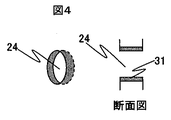
本実施例では、半田の盛上りを防止するために図2に示す透明基板12の嵌合穴24のメタライズ31を嵌合穴24側面のみに形成した。レンズ等の集光部品を用いない光直接結合系おいては、結合効率の観点から光素子13とファイバを近接させて配置することが望ましい。つまり、本構造においては透明基板12にコネクタを近接配置することが望ましい。従って、高効率な光結合効率を得るためには、ガイドピン11と嵌合穴24を封止した時に半田がコネクタ側へ盛上ることを防止してコネクタを透明基板12に近接配置する必要がある。そこで、半田がコネクタ側への盛上りを防止するために、図4が示すようにメタライズ31は嵌合穴24の側面のみに形成する。   In this embodiment, in order to prevent the solder from rising, the metallized 31 of the fitting hole 24 of the transparent substrate 12 shown in FIG. 2 is formed only on the side surface of the fitting hole 24. In an optical direct coupling system that does not use a condensing component such as a lens, it is desirable that the optical element 13 and the fiber be arranged close to each other from the viewpoint of coupling efficiency. That is, in this structure, it is desirable to place the connector close to the transparent substrate 12. Therefore, in order to obtain high optical coupling efficiency, it is necessary to prevent the solder from rising to the connector side when the guide pin 11 and the fitting hole 24 are sealed, and to place the connector close to the transparent substrate 12. is there. Therefore, in order to prevent the solder from rising to the connector side, the metallization 31 is formed only on the side surface of the fitting hole 24 as shown in FIG.

組立手順は実施例2と同じである。
以上述べた方法でモジュールを作製すれば、光素子13は気密に保たれ組立も調芯作業が無く作製でき、さらに気密封止も一回のリフロで簡単に行うことが出来、良好な光結合効率の光モジュールが作製できる。
The assembly procedure is the same as in the second embodiment.
If the module is manufactured by the above-described method, the optical element 13 can be kept airtight and assembled without any alignment work. Furthermore, the hermetic sealing can be easily performed by a single reflow, and excellent optical coupling is achieved. An efficient optical module can be produced.

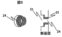
実施例3で述べたように高効率な光結合効率を得るためにコネクタを透明基板に近接配置する必要がある。本実施例では、図2に示す透明基板12の嵌合穴24構造を図5に示すように段差を利用しコネクタ側の凹部側面にはメタライズ31を形成せず、半田が透明基板12表面より盛上らないようにする構造である。   As described in the third embodiment, it is necessary to dispose the connector close to the transparent substrate in order to obtain high optical coupling efficiency. In this embodiment, the fitting hole 24 structure of the transparent substrate 12 shown in FIG. 2 is formed using a step as shown in FIG. It is a structure that prevents it from rising.

図5に示す嵌合穴24の作製は、まず透明基板12所定の2箇所に嵌合穴24より大きい凹部51を形成する。次に、その凹部底面に嵌合穴24を形成し段差構造の嵌合穴24を作製する。それから、凹部51にマスクをして、素子側の嵌合穴24のみにメタライズ31をする。メタライズの方法は蒸着、メッキ等どの方法を用いてもよい。メタライズ後凹部51のマスクを剥がし図5に示す段差嵌合穴を作製する。従って、凹部51にはメタライズを施さないため凹部側面に半田が濡れることが無いため、半田が盛上っても透明基板12の表面よりも高くならないように半田の量を調整すれば半田が透明基板12から盛上らずに透明基板12とコネクタ121を近接配置が可能となる。   5, the concave portions 51 larger than the fitting holes 24 are first formed at two predetermined positions of the transparent substrate 12. Next, a fitting hole 24 is formed on the bottom surface of the recess to produce a fitting hole 24 having a step structure. Then, the recess 51 is masked, and the metallization 31 is made only in the fitting hole 24 on the element side. Any method such as vapor deposition or plating may be used for the metallization. After the metallization, the mask of the recess 51 is peeled off to form a step fitting hole shown in FIG. Accordingly, since the concave portion 51 is not metallized, the side surface of the concave portion is not wetted with solder. Therefore, if the amount of solder is adjusted so that it does not become higher than the surface of the transparent substrate 12 even if the solder rises, the solder is transparent. The transparent substrate 12 and the connector 121 can be arranged close to each other without rising from the substrate 12.

組立手順は実施例2と同じである。
本実施例に示す嵌合穴24の作製方法は一例である。この他の作製方法としては穴のサイズの異なる透明基板を貼り合せて作製する等の方法もある。さらに、嵌合穴24の形や作製に本方法を用いずに、嵌合穴24側面の少なくとも一部にメタライズを施さない構造とすれば効果は同じである。
以上述べた方法でモジュールを作製すれば、光素子13は気密に保たれ組立も調芯作業が無く作製でき、さらに気密封止も一回のリフロで簡単に行うことが出来き、良好な光結合効率の光モジュールが作製できる。
The assembly procedure is the same as in the second embodiment.
The manufacturing method of the fitting hole 24 shown in the present embodiment is an example. As another manufacturing method, there is a method in which transparent substrates having different hole sizes are bonded to each other. Furthermore, the effect is the same if the structure is made without metallizing at least a part of the side surface of the fitting hole 24 without using the present method for the shape or production of the fitting hole 24.
If the module is manufactured by the above-described method, the optical element 13 is kept airtight and can be manufactured without assembling and aligning work. Further, the hermetic sealing can be easily performed by a single reflow, and a good light can be obtained. An optical module with coupling efficiency can be produced.

本実施例は、図2に示すガイドピン11と嵌合穴24を封止するために半田をリフロで溶解した時、半田がガイドピン11を伝って素子基板15および光素子13にまで流れてしまい、素子基板上15の配線パターン等を短絡させてしまう問題がある。そこで、図6に示すようにガイドピン11に段差61を設けて半田が素子基板に流れる事を防止する。段の位置は、透明基板12と封止リング14の固定には影響を与えず半田の流れを受け止める位置とするため、透明基板12から数十μm光素子側としている。   In this embodiment, when the solder is melted by reflow to seal the guide pin 11 and the fitting hole 24 shown in FIG. 2, the solder flows through the guide pin 11 to the element substrate 15 and the optical element 13. Therefore, there is a problem that the wiring pattern on the element substrate 15 is short-circuited. Therefore, as shown in FIG. 6, a step 61 is provided on the guide pin 11 to prevent the solder from flowing to the element substrate. The position of the step is set to the optical element side of several tens of μm from the transparent substrate 12 so as to receive the solder flow without affecting the fixing of the transparent substrate 12 and the sealing ring 14.

組立手順は実施例2と同じである。
以上述べた方法でモジュールを作製すれば、光素子13は気密に保たれ組立も調芯作業が無く作製でき、さらに気密封止も一回のリフロで簡単に行える。さらに、半田の濡れによる短絡不良を防ぎ、生産性よく良好な光モジュールを作製できる。
The assembly procedure is the same as in the second embodiment.
If the module is manufactured by the method described above, the optical element 13 is kept airtight, can be assembled without any alignment work, and can be easily hermetically sealed with a single reflow. Furthermore, it is possible to prevent a short circuit failure due to solder wetting and to produce a good optical module with high productivity.

本実施例は、実施例6で述べたようにガイドピン11と嵌合穴24を封止するため半田をリフロで溶解した時に、半田が図1に示すガイドピン11を伝って素子基板15および光素子13に流れてしまうと素子基板15上の配線パターン等を短絡させてしまう問題がある。また、半田がガイドピン11を伝ってコネクタ側に流れると実施例4で述べたようにコネクタを透明基板12に近接配置ができず高効率の光結合が得られない問題がある。つまり、半田が不要な箇所に流れることを防止する必要がある。そこで、図7に示すようにガイドピン11の一部のみメタライズ71を形成し半田が不要箇所に流れることを防止する。メタライズ71位置は透明基板12と同じ高さにしている。メタライズの作製方法は、蒸着、メッキ等どの方法でも構わない。   In this embodiment, as described in the sixth embodiment, when the solder is melted by reflow to seal the guide pin 11 and the fitting hole 24, the solder travels along the guide pin 11 shown in FIG. If it flows into the optical element 13, there is a problem that the wiring pattern on the element substrate 15 is short-circuited. Further, when the solder flows along the guide pins 11 to the connector side, there is a problem that the connector cannot be disposed close to the transparent substrate 12 as described in the fourth embodiment, and high-efficiency optical coupling cannot be obtained. That is, it is necessary to prevent the solder from flowing to an unnecessary part. Therefore, as shown in FIG. 7, only a part of the guide pin 11 is formed with the metallized 71 to prevent the solder from flowing to unnecessary portions. The position of the metallized 71 is the same height as the transparent substrate 12. Any method such as vapor deposition or plating may be used for the metallization.

組立手順は実施例2と同じである。
また、メタライズはガイドピン11全体にメタライズを形成した後で一部のメタライズを除去してダムを形成し半田が不要箇所に流れる事を防止した構造でも効果は同じである。
以上述べた方法でモジュールを作製すれば、光素子13は気密に保たれ組立も無調芯で作製でき、さらに気密封止も一回のリフロで簡単に行える。その上、半田の濡れによる短絡不良および結合効率劣化を抑圧して、生産性よく光結合効率の良い光モジュールを作製できる。
The assembly procedure is the same as in the second embodiment.
The effect of the metallization is the same even when the metallization is formed on the entire guide pin 11 and then a part of the metallization is removed to form a dam so that the solder is prevented from flowing to an unnecessary portion.
If the module is manufactured by the above-described method, the optical element 13 is kept airtight, can be assembled with no alignment, and can be easily hermetically sealed with a single reflow. In addition, an optical module with good productivity and high optical coupling efficiency can be manufactured by suppressing short circuit failure and coupling efficiency deterioration due to solder wetting.

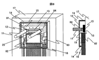
図8は本発明によるモジュール斜視図と断面図である。封止リング14の内側に、2本のガイドピン11、光素子13を搭載した素子基板15、集積回路82、バイパスコンデンサ83を所定の位置に配置し、各部品間をワイヤ19で接続している。さらに、封止リング14の開口部に透明基板12を固定し、ガイドピン11と透明基板12の隙間を半田84で埋めて封止リング14内の気密を保っている。   FIG. 8 is a perspective view and a sectional view of a module according to the present invention. Inside the sealing ring 14, the element substrate 15 on which the two guide pins 11, the optical element 13 are mounted, the integrated circuit 82, and the bypass capacitor 83 are arranged at predetermined positions, and the components are connected by wires 19. Yes. Further, the transparent substrate 12 is fixed to the opening of the sealing ring 14, and the gap between the guide pin 11 and the transparent substrate 12 is filled with the solder 84 to keep the sealing ring 14 airtight.

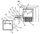
次に図9を参照して各部品の詳細な説明を行う。台座17にはガイドピン11と封止リング14が固定されている。このガイドピン11の間隔は精度良く固定されているが絶対位置に関しては特に精度を必要としない。また、封止リング14はガイドピン11位置を基準として台座17に溶接またはロウ付け等で固定している。さらに、封止リング14はセラミックの積層構造を用いて、封止リング内部と外部で信号の伝達を行う配線パターン18を設けている。また、台座は集積回路82、光素子13のヒートシンクの機能としても用いるため、熱伝導率の良い材質を使用すると良い。   Next, each component will be described in detail with reference to FIG. A guide pin 11 and a sealing ring 14 are fixed to the base 17. The distance between the guide pins 11 is fixed with high accuracy, but the accuracy is not particularly required with respect to the absolute position. Further, the sealing ring 14 is fixed to the pedestal 17 by welding or brazing or the like with respect to the position of the guide pin 11. Furthermore, the sealing ring 14 is provided with a wiring pattern 18 that transmits signals inside and outside the sealing ring by using a ceramic laminated structure. Further, since the pedestal is also used as a function of the heat sink of the integrated circuit 82 and the optical element 13, it is preferable to use a material having good thermal conductivity.

次に素子基板15について説明する。基板の表面にガイドピン11と嵌合する穴22とアライメントマーク21とAuSn半田23を設ける。前記アライメントマーク21と嵌合穴22は一回のフォトリソグラフィで形成し、相対位置は<±2μmの高精度とする。このアライメントマーク21付近に光素子13を搭載するためのAuSn半田23を設ける。また、素子基板15の厚さは、集積回路82の厚さと光素子13の厚さの差とし、集積回路82と光素子13の表面の高さを合せることでワイヤ19を短くして寄生インダクタンスを低減させ高周波特性を改善している。さらに配線パターン18の高さと集積回路82の表面高さも合わせて高周波特性を改善している。   Next, the element substrate 15 will be described. A hole 22 for fitting the guide pin 11, an alignment mark 21, and AuSn solder 23 are provided on the surface of the substrate. The alignment mark 21 and the fitting hole 22 are formed by a single photolithography, and the relative position is high accuracy of <± 2 μm. An AuSn solder 23 for mounting the optical element 13 is provided near the alignment mark 21. Further, the thickness of the element substrate 15 is the difference between the thickness of the integrated circuit 82 and the thickness of the optical element 13, and by matching the height of the surface of the integrated circuit 82 and the optical element 13, the wire 19 is shortened and the parasitic inductance is increased. To improve the high frequency characteristics. Further, the high frequency characteristics are improved by combining the height of the wiring pattern 18 and the surface height of the integrated circuit 82.

さらに、光素子13は12チャンネルアレイの面発光素子である。表面には発光点、電極パターンアライメントマークが形成され裏面にも素子基板15のAuSn半田23と固定するようにメタライズを施している。さらに、集積回路82は光素子駆動用のICであり信号の増幅等を行う。   Furthermore, the optical element 13 is a 12-channel array surface emitting element. A light emitting point and an electrode pattern alignment mark are formed on the front surface, and metallization is performed on the back surface so as to be fixed to the AuSn solder 23 of the element substrate 15. Further, the integrated circuit 82 is an IC for driving optical elements, and performs signal amplification and the like.

次に透明基板12について説明する。透明基板12は石英系のガラスを用いて作製し、周囲は封止リング14と固定するためのメタライズ32が形成されている。さらには、ガイドピン11と嵌合する嵌合穴24が2つあり、その周囲にはメタライズ31が施されている。また、嵌合穴24の間にはレンズアレイ81を形成し、光素子13とファイバとの結合効率を改善している。このレンズアレイ81は前記嵌合穴24と一回のフォトリソグラフィで形成しており相対位置が高精度に作製されている。   Next, the transparent substrate 12 will be described. The transparent substrate 12 is manufactured using quartz-based glass, and the periphery thereof is formed with a metallization 32 for fixing to the sealing ring 14. Furthermore, there are two fitting holes 24 for fitting with the guide pins 11, and a metallized 31 is provided around them. A lens array 81 is formed between the fitting holes 24 to improve the coupling efficiency between the optical element 13 and the fiber. The lens array 81 is formed with the fitting hole 24 by one photolithography, and the relative position is manufactured with high accuracy.

さらに、図9を参照してモジュール組立手順について説明する。まず、光素子13を素子基板15に搭載する。搭載の位置合わせは光素子13と素子基板15の両方に設けているアライメントマークを用いて行う。位置合わせ後、光素子13を素子基板15のAuSn半田23上に仮固定する。その後、窒素雰囲気下でリフロし本固定する。以上の工程により、光素子13は嵌合穴22に対して高精度に実装できる。なぜなら、先に述べたように嵌合穴22とアライメントマーク21は一回のフォトリソグラフィで作製しているため高精度に形成されており、このアライメントマーク21を用いて光素子13との位置合せを行い搭載しているからである。   Furthermore, the module assembly procedure will be described with reference to FIG. First, the optical element 13 is mounted on the element substrate 15. Mounting alignment is performed using alignment marks provided on both the optical element 13 and the element substrate 15. After alignment, the optical element 13 is temporarily fixed on the AuSn solder 23 of the element substrate 15. Then, reflow under a nitrogen atmosphere and fix it. Through the above steps, the optical element 13 can be mounted in the fitting hole 22 with high accuracy. This is because, as described above, the fitting hole 22 and the alignment mark 21 are formed with high precision because they are produced by one photolithography, and the alignment with the optical element 13 is performed using this alignment mark 21. This is because it is installed.

次にガイドピン11に各部品を挿入して光結合構造を作製する。まず、光素子13を搭載した素子基板15を嵌合穴22がガイドピン11と嵌合するように挿入して、台座17と接着剤で固定する。その後、集積回路82、バイパスコンデンサ83等の部品を封止リング14内の所定の位置に固定しワイヤ19で電気接続を行う。その後、透明基板12を嵌合穴24がガイドピン11と嵌合するように挿入する。そこから、透明基板12と封止リング14、およびガイドピン11と嵌合穴24の接続部分に半田を形成しモジュール全体をリフロして半田を溶解して接着する。   Next, each component is inserted into the guide pin 11 to produce an optical coupling structure. First, the element substrate 15 on which the optical element 13 is mounted is inserted so that the fitting hole 22 is fitted to the guide pin 11 and is fixed to the base 17 with an adhesive. Thereafter, components such as the integrated circuit 82 and the bypass capacitor 83 are fixed at predetermined positions in the sealing ring 14 and are electrically connected by the wire 19. Thereafter, the transparent substrate 12 is inserted so that the fitting holes 24 are fitted to the guide pins 11. From there, solder is formed on the connection portion of the transparent substrate 12 and the sealing ring 14, and the guide pin 11 and the fitting hole 24, and the entire module is reflowed to melt and bond the solder.

また、使用環境の温度変化等により透明基板を割れにくくする為に、透明基板12に封止リング14と線膨張係数の近い材質の透過セラミック等を選択するとより効果的である。また、透明基板12は一枚の基板で作製する必要がなく、光を透過する部分のみガラスや透過セラミック等の光の透過する基板を用いて光の透過しない部分には金属等を使用し前記光の透過する基板と金属を気密の保てる方法で接着して透明基板12を作製しても効果的である。また、本構造は面発光素子の変わりに端面発光素子や受光素子を用いても効果は同じである。
以上述べた方法でモジュールを作製すれば、光素子は気密に保たれ組立も調芯作業が無く作製でき、さらに気密封止も一回のリフロで簡単に行える。また、高周波特性がよく光結合効率も良い光モジュールを生産性よく作製できる。
Further, in order to make the transparent substrate difficult to break due to temperature changes in the usage environment, it is more effective to select a transparent ceramic or the like having a linear expansion coefficient close to that of the sealing ring 14 for the transparent substrate 12. In addition, the transparent substrate 12 does not need to be made of a single substrate, only a portion that transmits light uses a substrate that transmits light, such as glass or transmissive ceramic, and a portion that does not transmit light uses metal or the like. It is also effective to produce the transparent substrate 12 by bonding the light transmitting substrate and the metal in a manner that keeps the gas tight. In addition, this structure has the same effect even when an end face light emitting element or a light receiving element is used instead of the surface light emitting element.
If the module is manufactured by the above-described method, the optical element is kept airtight, can be manufactured without assembling and alignment, and can be easily hermetically sealed with a single reflow. In addition, an optical module having high frequency characteristics and good optical coupling efficiency can be manufactured with high productivity.

開示技術は、ガイドピンを用いて光素子とファイバの相対位置合わせを行う光モジュールの光結合構造に関するものであり、産業上の利用可能性を有する。   The disclosed technology relates to an optical coupling structure of an optical module that performs relative alignment between an optical element and a fiber using a guide pin, and has industrial applicability.

本発明における基本構造。The basic structure in this invention. 本発明構造の作製方法および部品。Manufacturing method and component of the structure of the present invention. 本発明における嵌合穴の実施例。The Example of the fitting hole in this invention. 本発明における嵌合穴の実施例。The Example of the fitting hole in this invention. 本発明における嵌合穴の実施例。The Example of the fitting hole in this invention. 本発明におけるガイドピンの実施例。The Example of the guide pin in this invention. 本発明におけるガイドピンの実施例。The Example of the guide pin in this invention. 本発明における実施例の構造。The structure of the Example in this invention. 本発明構造における実施例の作製方法および部品。Example manufacturing method and component in the structure of the present invention. 従来構造1。Conventional structure 1. 従来構造2。Conventional structure 2. ガイドピン用いた場合の基本的な光結合構造。Basic optical coupling structure when using guide pins.

符号の説明Explanation of symbols

11:ガイドピン
12:透明基板
13:光素子
14:封止リング
15:素子基板
16:封止材
17:台座
18:配線パターン
19:ワイヤ
21:アライメントマーク
22:素子基板嵌合穴
23:AuSn半田(素子搭載部)
24:透明基板嵌合穴
31:メタライズ
32:メタライズ
51:凹部
61:段差
71:メタライズ
81:レンズアレイ
82:集積回路
83:バイパスコンデンサ
84:半田
101:ガイドピン
102:第1フランジ
103:第2フランジ
104:光素子
105:レンズアレイ
106:パッケージ
107:集積回路
108:ワイヤ
109:配線パターン
111:素子基板
112:ガイドピン
113:台座
114:光素子
115:MTコネクタ
121:MTコネクタ
122:ファイバアレイ
123:嵌合穴
124:光素子
125:ガイドピン
126:リッド。
11: Guide pin
12: Transparent substrate
13: Optical element
14: Sealing ring
15: Element substrate
16: Sealing material
17: Pedestal
18: Wiring pattern
19: Wire
21: Alignment mark
22: Element board mating hole
23: AuSn solder (element mounting part)
24: Transparent substrate mating hole
31: Metallization
32: Metallization
51: recess
61: Step
71: Metallization
81: Lens array
82: Integrated circuit
83: Bypass capacitor
84: Solder
101: Guide pin
102: 1st flange
103: 2nd flange
104: Optical element
105: Lens array
106: Package
107: Integrated circuit
108: Wire
109: Wiring pattern
111: Element substrate
112: Guide pin
113: Pedestal
114: Optical element
115: MT connector
121: MT connector
122: Fiber array
123: Mating hole
124: Optical element
125: Guide pin
126: Lid.

Claims (11)

光素子と光導波路あるいは光ファイバの光結合を行う構造において、少なくとも光素子を配置する部分と2本のガイドピンを有し、該光素子配置部と該ガイドピンを内包するように気密封止するための封止リングで囲い、その該封止リングの開口部をガイドピンと嵌合する嵌合穴を有し使用波長に対して少なくても一部が透過する透明基板で塞ぎ、該ガイドピンと該透明基板の該嵌合穴の隙間を封止材で埋めて気密封止することを特徴とした光モジュール。 In a structure for optically coupling an optical element and an optical waveguide or an optical fiber, it has at least a portion where the optical element is arranged and two guide pins, and is hermetically sealed so as to enclose the optical element arrangement portion and the guide pin The sealing ring is enclosed with a transparent substrate that has a fitting hole for fitting with the guide pin, and at least a part of which is transparent to the wavelength used, and is sealed with the guide pin. An optical module, wherein a gap between the fitting holes of the transparent substrate is filled with a sealing material and hermetically sealed. 該透明基板の光が透過する部分がガラスであることを特徴とする請求項1の光モジュール。 2. The optical module according to claim 1, wherein the light transmitting portion of the transparent substrate is glass. 該透明基板の光が透過する部分が透過セラミックであることを特徴とする請求項1の光モジュール。 2. The optical module according to claim 1, wherein the light transmitting portion of the transparent substrate is a transmissive ceramic. 該封止材が接着材であることを特徴とする請求項1〜3の光モジュール。 The optical module according to claim 1, wherein the sealing material is an adhesive. 該封止材が半田であり、該透明基板の嵌合穴および該嵌合穴周辺にメタライズしていることを特徴とする請求項1〜3の光モジュール。 The optical module according to claim 1, wherein the sealing material is solder and is metallized around the fitting hole of the transparent substrate and around the fitting hole. 該透明基板の該メタライズが該嵌合穴の側面のみに形成されていることを特徴とする請求項5の光モジュール。   6. The optical module according to claim 5, wherein the metallization of the transparent substrate is formed only on the side surface of the fitting hole. 該透明基板には凹部があり該凹部に該嵌合穴を形成し、該凹部内壁の全面もしくは一部にメタライズがないことを特徴とする請求項5の光モジュール。   6. The optical module according to claim 5, wherein the transparent substrate has a recess, the fitting hole is formed in the recess, and the entire or part of the inner wall of the recess has no metallization. 該ガイドピンに段を設け、該半田が封止リング内に流れ込むことを防止する構造を有することを特徴とする請求項5〜7の光モジュール。 8. The optical module according to claim 5, wherein a step is provided on the guide pin to prevent the solder from flowing into the sealing ring. 該ガイドピンの一部にメタライズあるいは一部にのみ該半田が固着する構造を有することを特徴とする請求項5〜7の光モジュール。 8. The optical module according to claim 5, wherein said guide pin has a structure in which a part of said guide pin is metallized or said solder is fixed to only a part thereof. 該透明基板にはレンズ機能を有していることを特徴とする請求項1〜9の光モジュール。   The optical module according to claim 1, wherein the transparent substrate has a lens function. 該封止リング内に集積回路も具備している事を特徴とする請求項1〜10の光モジュール。
The optical module according to claim 1, further comprising an integrated circuit in the sealing ring.
JP2004111686A 2004-04-06 2004-04-06 Optical module Pending JP2005292738A (en)

Priority Applications (1)

Application Number Priority Date Filing Date Title
JP2004111686A JP2005292738A (en) 2004-04-06 2004-04-06 Optical module

Applications Claiming Priority (1)

Application Number Priority Date Filing Date Title
JP2004111686A JP2005292738A (en) 2004-04-06 2004-04-06 Optical module

Publications (1)

Publication Number Publication Date
JP2005292738A true JP2005292738A (en) 2005-10-20

Family

ID=35325686

Family Applications (1)

Application Number Title Priority Date Filing Date
JP2004111686A Pending JP2005292738A (en) 2004-04-06 2004-04-06 Optical module

Country Status (1)

Country Link
JP (1) JP2005292738A (en)

Cited By (1)

* Cited by examiner, † Cited by third party
Publication number Priority date Publication date Assignee Title
JP2007324303A (en) * 2006-05-31 2007-12-13 Hitachi Cable Ltd Optical module and mounting method thereof

Cited By (1)

* Cited by examiner, † Cited by third party
Publication number Priority date Publication date Assignee Title
JP2007324303A (en) * 2006-05-31 2007-12-13 Hitachi Cable Ltd Optical module and mounting method thereof

Similar Documents

Publication Publication Date Title
US9442255B2 (en) Low profile fiber-to-module interface with relaxed alignment tolerances
JP3998526B2 (en) Optical semiconductor package
US7837398B2 (en) Optical module having a block with feedthrough pins
CN102422193B (en) Optical subassembly with optical device having ceramic pacakge
US8475057B2 (en) Optical module with ceramic package
US7039083B2 (en) High speed optical transmission assembly
TW202441235A (en) Sealed optical transceiver
JP2008304903A (en) Optical assembly and method for forming the same
CN102377104A (en) Optical module with ceramic package
EP2753964B1 (en) Hermetic small form factor optical device packaging for plastic optical fiber networks
JP4212845B2 (en) Optical semiconductor element module
CN113341513B (en) Optical module
CN213240598U (en) Small-volume light emitting assembly and multichannel parallel optical device
US7255494B2 (en) Low-profile package for housing an optoelectronic assembly
JP2005292738A (en) Optical module
JP4807987B2 (en) Hermetically sealed package and optical submodule
JP5515182B2 (en) Optical module
US20050013558A1 (en) Integrated fiber attach pad for optical package
JP2004029161A (en) Optical semiconductor device module
US20250093599A1 (en) Optical module assembly
JPH11174280A (en) Semiconductor laser module and metallic ferrule
JP2000089065A (en) Optical module and method of manufacturing the same
CN118380853A (en) TO packaged light emitting component and packaging method thereof
JPH0422907A (en) Photodetecting module and its production
JP2000199831A (en) Optical module

Legal Events

Date Code Title Description
RD04 Notification of resignation of power of attorney

Free format text: JAPANESE INTERMEDIATE CODE: A7424

Effective date: 20060424