JP2005292572A - Light source device - Google Patents
Light source device Download PDFInfo
- Publication number
- JP2005292572A JP2005292572A JP2004109093A JP2004109093A JP2005292572A JP 2005292572 A JP2005292572 A JP 2005292572A JP 2004109093 A JP2004109093 A JP 2004109093A JP 2004109093 A JP2004109093 A JP 2004109093A JP 2005292572 A JP2005292572 A JP 2005292572A
- Authority
- JP
- Japan
- Prior art keywords
- holding member
- fixing
- light source
- optical waveguide
- generation element
- Prior art date
- Legal status (The legal status is an assumption and is not a legal conclusion. Google has not performed a legal analysis and makes no representation as to the accuracy of the status listed.)
- Withdrawn
Links
Images


Landscapes
- Optical Couplings Of Light Guides (AREA)
- Optical Modulation, Optical Deflection, Nonlinear Optics, Optical Demodulation, Optical Logic Elements (AREA)
Abstract
【課題】光源装置の製造歩留まりを可及的に向上させる。
【解決手段】レーザ光源LSと、光導波路型の第2高調波発生素子41と、レーザ光源LSの出射レーザ光を前記第2高調波発生素子41へ導く光ファイバ36とが備えられ、前記光ファイバ36における光出射端近くが保持部材37にて保持されている光源装置において、前記保持部材37又は前記保持部材37に連設される固定用部材43を固定するための受け面RSが、前記第2高調波発生素子41の光導波路の長手方向と平行な仮想線に交差する姿勢で配置され、前記保持部材37又は前記固定用部材43において前記受け面RSと対向する面と前記受け面RSとの間が、液状状態を経て固着させる固着手段にて固着されて構成されている。
【選択図】図1The manufacturing yield of a light source device is improved as much as possible.
A laser light source LS, an optical waveguide type second harmonic generation element 41, and an optical fiber 36 for guiding the laser beam emitted from the laser light source LS to the second harmonic generation element 41 are provided. In the light source device in which the vicinity of the light emitting end of the fiber 36 is held by the holding member 37, the receiving surface RS for fixing the holding member 37 or the fixing member 43 connected to the holding member 37 is The second harmonic generation element 41 is disposed in a posture intersecting with an imaginary line parallel to the longitudinal direction of the optical waveguide, and the holding member 37 or the fixing member 43 faces the receiving surface RS and the receiving surface RS. Is fixed by fixing means for fixing through a liquid state.
[Selection] Figure 1
Description
本発明は、レーザ光源と、光導波路型の第2高調波発生素子と、レーザ光源の出射レーザ光を前記第2高調波発生素子へ導く光ファイバとが備えられ、前記光ファイバにおける光出射端近くが保持部材にて保持されている光源装置に関する。 The present invention includes a laser light source, an optical waveguide type second harmonic generation element, and an optical fiber that guides laser light emitted from the laser light source to the second harmonic generation element, and a light emission end of the optical fiber. The present invention relates to a light source device that is held nearby by a holding member.
かかる光源装置は、レーザ光源の出射光を第2高調波発生素子の光導波路に入射させて、入射レーザ光の1/2の波長の第2高調波を取り出す装置である。
このような光源装置においては、レーザ光源から出射したレーザ光を第2高調波発生素子の光導波路に効率良く入射させる必要があり、レンズを主体とする光学系で半導体レーザ素子の出射レーザ光を前記光導波路の光入射端面に集光する構成の他に、下記特許文献1に記載のように、半導体レーザ素子の出射光を光ファイバにて第2高調波発生素子の光導波路へ導く構成も考えられている。
下記特許文献1では、光ファイバの支持部材にV字状溝を形成して、そのV字状溝に光ファイバの先端部分を固定することで、第2高調波発生素子に対する光ファイバの光出射端の位置決めを行っている。
Such a light source device is a device that takes out light emitted from a laser light source into an optical waveguide of a second harmonic generation element and extracts a second harmonic having a wavelength half that of the incident laser light.
In such a light source device, the laser light emitted from the laser light source needs to be efficiently incident on the optical waveguide of the second harmonic generation element, and the emitted laser light from the semiconductor laser element is emitted by an optical system mainly composed of lenses. In addition to the configuration for condensing on the light incident end face of the optical waveguide, there is also a configuration for guiding the emitted light of the semiconductor laser element to the optical waveguide of the second harmonic generation element with an optical fiber as described in
In the following
上記のような位置決め構成では、光ファイバの光出射端の位置調整自由度が制限されるため、特願2004−64451号に記載のように、光ファイバの光出射端近くを保持部材にて保持すると共に、その保持部材を支持台上に固定する構成も考えられている。
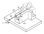
この保持部材による支持構成を示す図7のように、光ファイバ36の保持部材37を支持台101上に固定する前は、保持部材37は支持台101の支持面と平行方向に調整自由度を有しており、更に、保持部材37を支持台上に載置したときに、光ファイバの光出射端が第2高調波発生素子41の光導波路の位置よりもわずかに下方に位置するように支持台101の高さを設定することで、支持面の法線方向にも調整自由度を持たせることができる。
As shown in FIG. 7 showing the support structure by the holding member, before the
しかしながら、上述のような支持構成で保持部材を支持台上に固定すると、光源装置の製造歩留まりが低下してしまう不都合があった。
すなわち、接着剤あるいはYAG溶接等の液状状態を経て硬化する固着手段によって、光ファイバの保持部材を支持台上に固着させると、光ファイバの光出射端と第2高調波発生素子の光入射端とが位置ずれして、光ファイバから出射した光のうちの前記光導波路に入射する光の割合(すなわち、結合効率)が低下してしまい、実用に適さない不良品となってしまう場合があった。
本発明は、かかる実情に鑑みてなされたものであって、その目的は、光源装置の製造歩留まりを可及的に向上させる点にある。
However, when the holding member is fixed on the support base with the above-described support configuration, there is a disadvantage that the manufacturing yield of the light source device is lowered.
That is, when the holding member of the optical fiber is fixed on the support base by the fixing means that is cured through a liquid state such as an adhesive or YAG welding, the light emitting end of the optical fiber and the light incident end of the second harmonic generating element And the ratio of light entering the optical waveguide out of the light emitted from the optical fiber (that is, the coupling efficiency) is reduced, resulting in a defective product that is not suitable for practical use. It was.
The present invention has been made in view of such circumstances, and an object thereof is to improve the production yield of the light source device as much as possible.
本出願の第1の発明は、レーザ光源と、光導波路型の第2高調波発生素子と、レーザ光源の出射レーザ光を前記第2高調波発生素子へ導く光ファイバとが備えられ、前記光ファイバにおける光出射端近くが保持部材にて保持されている光源装置において、前記保持部材又は前記保持部材に連設される固定用部材を固定するための受け面が、前記第2高調波発生素子の光導波路の長手方向と平行な仮想線に交差する姿勢で配置され、前記保持部材又は前記固定用部材において前記受け面と対向する面と前記受け面との間が、液状状態を経て固着させる固着手段にて固着されて構成されている。 A first invention of the present application includes a laser light source, an optical waveguide type second harmonic generation element, and an optical fiber that guides the laser beam emitted from the laser light source to the second harmonic generation element. In the light source device in which the vicinity of the light emitting end of the fiber is held by the holding member, the receiving surface for fixing the holding member or the fixing member connected to the holding member is the second harmonic generation element. The holding member or the fixing member is fixed in a liquid state between the surface facing the receiving surface and the receiving surface. It is configured to be fixed by a fixing means.
すなわち、例えば接着剤の硬化時や溶接による硬化時のように液状状態から固化する過程においてその固着部分が収縮し、図7のような支持構成で光ファイバの保持部材を支持台上に固着手段で固着させた場合では、保持部材の位置ずれは、矢印Pで示すように、主に保持部材37の支持面の法線方向で発生する。
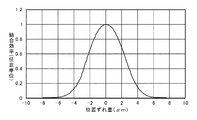
本発明の発明者が、第2高調波発生素子の光導波路の長手方向と直交する方向で保持部材を位置ずれさせたときの光ファイバと前記光導波路との結合効率の変化を測定したところ、図8のような特性が得られた。図8は、光導波路の横幅方向に保持部材を移動させた場合の測定例を示しており、光導波路の縦幅方向に保持部材を移動させた場合もほぼ同様である。但し、第2高調波発生素子での光導波路の形成形態として最も一般的な形態である光導波路の1側が素子表面に露出している形態の第2高調波発生素子を用いた場合は、若干非対称の形状となる。
いずれにしても、第2高調波発生素子の光導波路の長手方向と直交する方向で保持部材を位置ずれさせたときは、わずかな位置ずれで結合効率が大きく変化している。
従って、図7のような支持構成で光ファイバの保持部材を固着させると、結合効率が低下して不良品となってしまう確率が高くなってしまうのである。
That is, in the process of solidifying from a liquid state, for example, when the adhesive is cured or when cured by welding, the fixing portion contracts, and the optical fiber holding member is fixed on the support base in the support configuration as shown in FIG. As shown by the arrow P, the positional deviation of the holding member occurs mainly in the normal direction of the support surface of the
When the inventor of the present invention measured the change in the coupling efficiency between the optical fiber and the optical waveguide when the holding member was displaced in the direction orthogonal to the longitudinal direction of the optical waveguide of the second harmonic generation element, Characteristics as shown in FIG. 8 were obtained. FIG. 8 shows a measurement example when the holding member is moved in the horizontal width direction of the optical waveguide, and the same is true when the holding member is moved in the vertical width direction of the optical waveguide. However, when the second harmonic generation element having a form in which one side of the optical waveguide, which is the most common form of optical waveguide formation in the second harmonic generation element, is exposed on the element surface, is used. It becomes an asymmetrical shape.
In any case, when the holding member is displaced in the direction orthogonal to the longitudinal direction of the optical waveguide of the second harmonic generation element, the coupling efficiency changes greatly with a slight displacement.
Therefore, if the optical fiber holding member is fixed with the support structure as shown in FIG. 7, the coupling efficiency is lowered and the probability of being a defective product increases.
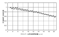
一方、本発明の発明者が、第2高調波発生素子の光導波路の長手方向に沿って保持部材を移動させたとき(すなわち、光ファイバの光出射端と光導波路の光入射端面との間の距離を変化させたとき)の光ファイバと前記光導波路との結合効率の変化を測定したところ、図9のような特性が得られた。
図9では、保持部材の変位に対して結合効率の低下は緩やかである。
従って、保持部材あるいは固定用部材の固着時に発生する位置変動が、光導波路の長手方向で発生するのであれば、固着時の位置変動に起因する結合効率の低下を抑制できることになる。
On the other hand, when the inventor of the present invention moves the holding member along the longitudinal direction of the optical waveguide of the second harmonic generation element (that is, between the light emitting end face of the optical fiber and the light incident end face of the optical waveguide). When the change in the coupling efficiency between the optical fiber and the optical waveguide was measured, the characteristics shown in FIG. 9 were obtained.
In FIG. 9, the decrease in coupling efficiency is moderate with respect to the displacement of the holding member.
Therefore, if the positional fluctuation that occurs when the holding member or the fixing member is fixed occurs in the longitudinal direction of the optical waveguide, it is possible to suppress a decrease in coupling efficiency due to the positional fluctuation at the time of fixing.
そこで、光ファイバの保持部材又は光ファイバの保持部材に連設される固定用部材を固定するための受け面を、第2高調波発生素子の光導波路の長手方向と平行な仮想線に交差する姿勢で配置し、前記保持部材又は前記固定用部材において前記受け面と対向する面と前記受け面との間を、液状状態を経て固着させる固着手段にて固着させる。
これによって、前記保持部材自体あるいは前記固定用部材を固着させたときに硬化時の収縮が発生しても、前記光導波路の長手方向に直交する方向での変位成分が相対的に小さくなる。
Therefore, the receiving surface for fixing the holding member of the optical fiber or the fixing member connected to the holding member of the optical fiber intersects a virtual line parallel to the longitudinal direction of the optical waveguide of the second harmonic generation element. It arrange | positions with an attitude | position and it fixes with the fixing | fixed means to fix between the surface facing the said receiving surface in the said holding member or the said fixing member, and the said receiving surface through a liquid state.
As a result, even if the holding member itself or the fixing member is fixed and shrinkage during curing occurs, the displacement component in the direction perpendicular to the longitudinal direction of the optical waveguide is relatively small.
又、本出願の第2の発明は、上記第1の発明の構成に加えて、前記受け面が、前記第2高調波発生素子を支持する支持台の1側面として形成されている。
すなわち、前記保持部材の存在位置を第2高調波発生素子の存在位置に対して固定するための前記受け面を、第2高調波発生素子を支持する支持台の一部を兼用して構成しているのである。
According to a second invention of the present application, in addition to the configuration of the first invention, the receiving surface is formed as one side surface of a support base that supports the second harmonic generation element.
That is, the receiving surface for fixing the existence position of the holding member with respect to the existence position of the second harmonic generation element is configured to also serve as a part of a support base that supports the second harmonic generation element. -ing
又、本出願の第3の発明は、上記第1又は上記第2の発明の構成に加えて、前記保持部材が、前記光導波路の長手方向と平行で且つ互いに平行な一対の側面を備えて形成され、前記固定用部材に、前記保持部材の前記一対の側面と対向する一対の案内面を備える案内溝が形成され、前記固定部材の支持面の法線方向が、前記一対の案内面の法線方向及び前記光導波路の長手方向に直交するように構成され、前記一対の側面と前記一対の案内面との間が、夫々、液状状態を経て固着させる固着手段にて固着されている。 According to a third invention of the present application, in addition to the configuration of the first or second invention, the holding member includes a pair of side surfaces parallel to the longitudinal direction of the optical waveguide and parallel to each other. And a guide groove having a pair of guide surfaces facing the pair of side surfaces of the holding member is formed in the fixing member, and a normal direction of a support surface of the fixing member is set to be It is configured to be orthogonal to the normal direction and the longitudinal direction of the optical waveguide, and the pair of side surfaces and the pair of guide surfaces are fixed by fixing means for fixing through a liquid state.
すなわち、光源装置の組み立て工程において、先ず、適宜に、光ファイバの保持部材を前記固定用部材の案内溝に沿って移動させつつ、前記固定用部材を前記支持面上で移動させて、光ファイバの光出射端が前記光導波路の光入射端に対して適正位置に位置するように調整し、前記保持部材と前記固定用部材とを前記固着手段にて固定する。
このとき、前記保持部材の互いに平行な一対の側面を同時に固着させることで、硬化時の収縮によって作用する力がバランスして、前記保持部材自体の位置変動が抑制される。
この保持部材の固着時に位置変動が発生しても、更に、前記固定用部材を位置調整してその位置変動を吸収できる。もちろん、前記保持部材の位置調整を精密に行っておけば、このときの前記固定用部材の位置調整量はわずかなもので済ませることができる。
そして、この固定用部材を固定するときは、上述のように、硬化時の収縮が発生しても、光ファイバと光導波路との結合効率の低下は十分に抑制できる。
尚、前記保持部材を前記固定用部材に固着させるための固着手段と、前記固定用部材を前記受け面に固着させるための固着手段とは、同一の固着手段であっても良いし、異なる固着手段であっても良い。
That is, in the assembly process of the light source device, first, the holding member for the optical fiber is moved along the guide groove of the fixing member, and the fixing member is moved on the support surface as appropriate. The light emitting end of the optical waveguide is adjusted so as to be positioned at an appropriate position with respect to the light incident end of the optical waveguide, and the holding member and the fixing member are fixed by the fixing means.
At this time, by fixing a pair of parallel side surfaces of the holding member at the same time, the force acting by the shrinkage at the time of curing is balanced, and the position variation of the holding member itself is suppressed.
Even if the position change occurs when the holding member is fixed, the position of the fixing member can be further adjusted to absorb the position change. Of course, if the position adjustment of the holding member is performed precisely, the position adjustment amount of the fixing member at this time can be small.
And when fixing this fixing member, even if shrinkage | contraction at the time of hardening generate | occur | produces as mentioned above, the fall of the coupling efficiency of an optical fiber and an optical waveguide can fully be suppressed.
The fixing means for fixing the holding member to the fixing member and the fixing means for fixing the fixing member to the receiving surface may be the same fixing means or different fixings. It may be a means.
上記第1の発明によれば、前記保持部材自体あるいは前記固定用部材を固着させたときに硬化時の収縮が発生しても、前記光導波路の長手方向に直交する方向での変位成分が相対的に小さくなるので、光ファイバと第2高調波発生素子の光導波路との結合効率の低下を十分に抑制できるものとなり、光源装置の製造歩留まりを可及的に向上させることができる。
又、上記第2の発明によれば、前記保持部材の存在位置を第2高調波発生素子の存在位置に対して固定するための前記受け面を、第2高調波発生素子を支持する支持台の一部を兼用して構成することで、光ファイバの光出射端の支持構成を簡素化することができる。
又、上記第3の発明によれば、前記保持部材を前記固定用部材に固着させるときに、前記保持部材自体の位置変動が抑制されるので、全体として位置調整作業を迅速に行うことができ、しかも、光ファイバと第2高調波発生素子の光導波路との結合効率の低下を抑制して、光源装置の製造歩留まりを向上させることができる。
According to the first aspect of the present invention, even when the holding member itself or the fixing member is fixed and shrinkage during curing occurs, the displacement component in the direction perpendicular to the longitudinal direction of the optical waveguide is relatively Therefore, the reduction in the coupling efficiency between the optical fiber and the optical waveguide of the second harmonic generation element can be sufficiently suppressed, and the production yield of the light source device can be improved as much as possible.
According to the second aspect of the invention, the receiving surface for fixing the holding position of the holding member with respect to the position of the second harmonic generation element is used as a support for supporting the second harmonic generation element. By using a part of this as well, it is possible to simplify the support structure of the light emitting end of the optical fiber.
According to the third aspect of the present invention, when the holding member is fixed to the fixing member, the position variation of the holding member itself is suppressed, so that the position adjustment operation can be performed quickly as a whole. In addition, it is possible to improve the manufacturing yield of the light source device by suppressing the decrease in the coupling efficiency between the optical fiber and the optical waveguide of the second harmonic generation element.
以下、本発明の光源装置を写真プリントシステムにおける露光用の光源として備えた場合の実施の形態を図面に基づいて説明する。
本実施の形態で例示する写真プリントシステムDPは、いわゆるデジタルミニラボ機として知られているものであり、図6のブロック構成図に示すように、各種の画像データ入力機器から写真プリントを作製するための画像データを入力する画像入力装置IRと、画像入力装置IRにて入力した画像データに基づいて印画紙2に露光処理する露光・現像装置EPとから構成されている。
Hereinafter, an embodiment in which the light source device of the present invention is provided as a light source for exposure in a photographic print system will be described with reference to the drawings.
The photographic print system DP exemplified in the present embodiment is known as a so-called digital minilab machine, and is for producing photographic prints from various image data input devices as shown in the block diagram of FIG. The image input device IR for inputting the image data, and the exposure / development device EP for exposing the
〔画像入力装置IRの概略構成〕
画像入力装置IRには、図6に概略的に示すように、写真フィルムの駒画像を読み取ってデジタル画像データとして出力するフィルムスキャナ3と、メモリーリーダ,MOドライブ及びCD−Rドライブ等の画像データ入力機器を備えた外部入出力装置4と、パーソナルコンピュータにて構成されてフィルムスキャナ3や外部入出力装置4の制御のほか写真プリントシステムDP全体の管理を実行する主制御装置5とが備えられ、更に、主制御装置5には、仕上がりプリント画像をシミュレートしたシミュレート画像や各種の制御用の情報を表示するモニタ5aと、露光条件の手動設定等や制御情報の入力操作をするための操作卓5bとが接続されている。
[Schematic configuration of image input device IR]
As schematically shown in FIG. 6, the image input device IR includes a
〔露光・現像装置EPの全体構成〕
露光・現像装置EPは、筐体内部に、画像露光装置EXと、画像露光装置EXにて露光された印画紙2を現像処理する現像処理装置PPと、印画紙マガジン6から引き出された印画紙2を多数の搬送ローラ9等にて現像処理装置PPへ搬送する印画紙搬送系PTとが設けられている。
図示を省略するが、露光・現像装置EPの筐体外部には、現像処理装置PPにて現像処理及び乾燥処理された印画紙2をオーダ毎に分類するためのソータが備えられ、現像処理装置PPの印画紙排出口から排出された印画紙2をこのソータへ搬送するコンベア10が筐体上面に備えられている。
更に、印画紙搬送系PTの搬送経路の途中には、印画紙マガジン6から引き出された長尺の印画紙2を設定プリントサイズに切断するカッタ11と、印画紙2の搬送列を複数の搬送列に振り分けるための振り分け装置12とが備えられている。
[Overall configuration of exposure / development apparatus EP]
The exposure / development apparatus EP includes an image exposure apparatus EX, a development processing apparatus PP for developing the
Although not shown, a sorter is provided outside the housing of the exposure / development apparatus EP to classify the
Further, in the middle of the conveyance path of the photographic paper conveyance system PT, a
〔画像露光装置EXの構成〕
画像露光装置EXは、印画紙2に画像を露光形成する露光ユニット13と、露光ユニット13を制御する露光制御装置14とを主要部として構成されている。
〔露光ユニット13の構成〕
露光ユニット13は、強度変調された光ビームを印画紙2上で走査して、印画紙2上に画像を露光形成するいわゆるレーザビーム露光式を採用しており、その概略構成を図5のブロック構成図に示す。
露光ユニット13には、赤色光源装置21と、緑色光源装置22と、青色光源装置23と、緑色光源装置22及び青色光源装置23から出射した光ビームを強度変調するための音響光学変調素子24(以下、「AOM素子24」と略記する)と、光ビームの光路を屈曲させるミラー25と、球面レンズ26と、シリンドリカルレンズ27と、図示を省略するモータにて回転駆動されるポリゴンミラー28と、f−θ特性と面倒れ補正機能とを有するレンズ群29とが備えられている。
[Configuration of image exposure apparatus EX]
The image exposure apparatus EX is composed mainly of an
[Configuration of Exposure Unit 13]
The
The
〔光源装置21,22,23の構成〕
赤色光源装置21は、図示を省略するが、赤色半導体レーザ素子と赤色半導体レーザ素子の出射光を集光する集光レンズとが備えられ、緑色光源装置22及び青色光源装置23と異なり、半導体レーザ素子の駆動電流を直接変調することによって出射レーザビームを強度変調している。
緑色光源装置22と青色光源装置23とは基本的な構成は共通であり、これらの構成を緑色光源装置22によって代表して説明する。
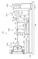
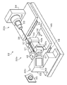
図1の側面図及び図4の斜視図に示すように、緑色光源装置22には、近赤外半導体レーザ装置22aと、近赤外半導体レーザ装置22aの出射レーザ光の第2高調波を生成する第2高調波発生装置22bと、フィルタユニット22cと、フィルタユニット22cを通過した第2高調波の光ビームをAOM素子24の受光開口に集光するための集光レンズユニット22dとが備えられている。
近赤外半導体レーザ装置22a,第2高調波発生装置22b及びフィルタユニット22cは、支持板65上に取り付けられ、更に、その支持板65と集光レンズユニット22dとが基礎支持板66上に取り付けられている。
[Configuration of
Although not shown, the red
The green
As shown in the side view of FIG. 1 and the perspective view of FIG. 4, the green
The near-infrared
近赤外半導体レーザ装置22aには、図1に示すように、レーザ光源LSである半導体レーザ素子31を収納したレーザ筐体32と、レーザ筐体32の光出射開口側に取り付けられて光ファイバ36の一端を支持するファイバ支持部材33と、レーザ筐体32を支持するレーザ支持台34と、半導体レーザ素子31の温度調整をするための熱電冷却装置35とが備えられ、半導体レーザ素子31の出射光は、半導体レーザ素子31の光出射位置に正確に位置決めされた光ファイバ36にて第2高調波発生装置22bへ導かれる。
この光ファイバ36は、コアの部分において光軸方向に一定周期で屈折率を変化させた、いわゆるファイバブラッググレーティングを形成しており、このファイバブラッググレーティングの作用によって半導体レーザ素子31の発光波長及び光出力を安定化している。
As shown in FIG. 1, the near-infrared
The
第2高調波発生装置22bには、細長い薄板状の第2高調波発生素子41と、第2高調波発生素子41を支持する支持台42と、光ファイバ36の光出射端近くを保持する保持部材37に連設される状態で保持部材37を第2高調波発生素子41に対して位置決め固定するための固定用部材43と、第2高調波発生素子41の光出射端面近傍に配置されて第2高調波発生素子41の出射光をコリメートするコリメートレンズ44と、コリメートレンズ44を支持するレンズ支持部材45とが備えられている。
支持台42は、第2高調波発生素子41を支持するSHG支持部42aと、レンズ支持部材45を支持するレンズ支持部42bと、これら支える基台部42cとが一体形成され、基台部42cの上面が固定用部材43を支持する支持面SSになっている。
この支持台42は、更に、第2高調波発生素子41を温度制御するための熱電冷却装置46上に支持されている。
The second
In the
The
第2高調波発生素子41は、光導波路型の第2高調波発生素子であり、第2高調波発生素子41の長手方向全長に亘って光導波路が形成されている。
従って、第2高調波発生素子41の長手方向が光導波路の長手方向であり、これは、光ファイバ36の光出射端から出射した光の光軸方向でもある。以下において、この第2高調波発生素子41の光導波路の長手方向を、単に「光導波路方向」と略称する場合がある。
第2高調波発生素子41の光導波路には、それの長手方向で周期分極反転構造が形成されている。この光導波路の一端(光入射端面)に光ファイバ36の光出射端が保持部材37に支持された状態で位置決めされている。
本実施の形態では、第2高調波発生素子41の基板としてLiNbO3を用いており、光導波路はプロトン交換法等により形成し、周期分極反転構造は、電界印加法あるいはTi拡散法等で周期的に分極を反転させることにより形成する。
The second
Therefore, the longitudinal direction of the second harmonic generating
A periodic polarization inversion structure is formed in the longitudinal direction of the optical waveguide of the second
In the present embodiment, LiNbO 3 is used as the substrate of the second
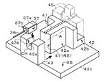
保持部材37を固定するための固定用部材43は、組み立て前の第2高調波発生装置22bをレーザ光源LS側からの斜視図で示す図3のように、全体としては光導波路方向での寸法が短い直方体形状に形成され、上部に、保持部材37を受け入れる案内溝CHが縦溝として形成されている。
保持部材37の外形形状は、光導波路方向での寸法が長い略直方体形状に形成され、保持部材37を固定用部材43へ取り付けるために案内溝CHへ挿入したときに、保持部材37の縦姿勢の一対の側面37a,37bが、案内溝CHの縦姿勢の一対の案内面43a,43bと夫々対向する。
この一対の側面37a,37bと一対の案内面43a,43bとの間が夫々、液状状態を経て固着させる固着手段の1例である接着剤(紫外線硬化型)にて固着される。
The fixing
The outer shape of the holding
The pair of
固定用部材43は、第2高調波発生素子41の光入射端面と略面一の縦壁面47に当てつける状態で、縦壁面47と固定用部材43において縦壁面47に対向する面との間が、前記固着手段の1例である接着剤(紫外線硬化型)にて固着される。
従って、支持台42の縦壁面47は、保持部材37に連設される固定用部材43を固定するための受け面RSとして機能しており、光導波路方向と平行な仮想線Aに交差する(具体的には、直交する)姿勢で配置されている。
The fixing
Therefore, the
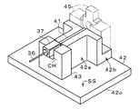
第2高調波発生素子41の光導波路の光入射端面に対して光ファイバ36の光出射端を位置調整して固定するときは、先ず、図2に示すように、保持部材37を固定用部材43の案内溝CHへ挿入した状態で、固定用部材43をSHG支持部42aの縦壁面47(受け面RS)に当てつけた状態とする。
保持部材37の一対の側面37a,37b及び案内溝CHの一対の案内面43a,43bは光導波路方向と平行で、固定用部材43を支持する支持面SSの法線方向は、案内面43a,43bの法線方向及び光導波路方向に直交しており、図2の状態では、図示を省略するマニピュレータで保持部材37をホールドして、水平軸,垂直軸及び光導波路方向の計3軸で移動調整できる。
When fixing the light emitting end of the
The pair of
図2の状態で、第2高調波発生素子41の光出力をモニタしながら保持部材37を移動調整し、光軸が合うと、保持部材37の一対の側面37a,37bと固定用部材43の一対の案内面43a,43bとの間を夫々接着剤にて固着させる。
次に、図示を省略するマニピュレータにて固定用部材43をホールドして、第2高調波発生素子41の光出力をモニタしながら、主に支持面SSと平行方向に移動調整する。保持部材37の基本的な位置調整は既に終了しており、又、保持部材37の固着時の位置変動もわずかであるため、固定用部材43の位置調整量はごくわずかである。
固定用部材43の位置調整が完了すると、縦壁面47と固定用部材43における縦壁面47に対向する面との間を接着剤にて固着させる。
このとき、極力、塗布する接着剤が固定用部材43の底面側に回り込んでしまわないようにする。
固定用部材43の固着時に光導波路方向で若干の位置変動が発生するが、この位置変動が光ファイバ36と第2高調波発生素子41の光導波路との結合効率に与える影響はごくわずかである。
固定用部材43の固定後、保持部材37から露出した光ファイバ36の光出射端と第2高調波発生素子41の光入射端面との間に、取付け状態を安定的に保持するため、及び、各界面でのレーザ光の反射を抑制するために、光学用の接着剤を充填して硬化させる。
この後、更に、コリメートレンズ44を取り付けたレンズ支持部材45を、レンズ支持部42b上に載置し、コリメートレンズ44の位置調整を行った後に固定する。
In the state of FIG. 2, the holding
Next, the fixing
When the position adjustment of the fixing
At this time, as much as possible, the adhesive to be applied is prevented from going around the bottom surface of the fixing
When the fixing
In order to stably hold the mounting state between the light emitting end of the
Thereafter, the
フィルタユニット22cは、第2高調波発生素子41の出射光から基本波の波長成分を吸収除去するための赤外吸収フィルタ51と、赤外吸収フィルタ51を通過した第2高調波の一部をフォトダイオード55に向けて反射するビームスプリッタ52と、これらの部品を支持する支持台53とが備えられている。
支持台53には、赤外吸収フィルタ51を通過した第2高調波をビームスプリッタ52へ向けて通過させるための入射側貫通孔53aと、ビームスプリッタ52で反射された第2高調波をフォトダイオード55へ向けて通過させるための反射側貫通孔53bとが形成されている。
緑色光源装置22の実使用時においては、ビームスプリッタ52で反射された第2高調波の一部をフォトダイオード55が検出すると、その検出信号は、図示を省略するAPC回路へ入力されて、フォトダイオード55の検出信号が一定値となるように半導体レーザ素子31の駆動電流が調節される。
The
The
When the green
集光レンズユニット22dには、図1に示すように、集光レンズ61と、集光レンズ61を支持するレンズホルダ62と、レンズホルダ62を支持するレンズ支持台63とが備えられ、レンズ支持台63には、ビームスプリッタ52を透過した第2高調波を通過させるための貫通孔63aが形成されている。
以上、緑色光源装置22の構成として説明したが、上述のように、青色光源装置23の構成要素は緑色光源装置22の構成要素と共通であり、使用する半導体レーザ素子の発振波長や、第2高調波発生素子の周期分極反転構造の周期等の、光の波長に関する部分が異なる。
As shown in FIG. 1, the
The configuration of the green
〔露光制御装置14の構成〕
露光制御装置14には、図5に概略的に示すように、上記構成の露光ユニット13を制御するために、画像入力装置IRから入力される赤色,緑色及び青色夫々の露光用画像データを露光ユニット13の露光特性を考慮した画像データに補正するルックアップテーブル71と、ルックアップテーブル71にて補正された画像データを赤色,緑色及び青色の各色毎に記憶する画像データメモリ72と、赤色,緑色及び青色の各色毎に備えられて画像データメモリ72の出力データをD/A変換するD/Aコンバータ73と、緑色及び青色についてD/Aコンバータ73からの入力信号に応じて変調されたAOM素子24の駆動信号を生成するAOM制御回路74と、赤色についてD/Aコンバータ73からの入力信号に応じて赤色光源装置21の半導体レーザ素子の駆動電流を変調するLD駆動回路75とが備えられている。
[Configuration of Exposure Control Device 14]
As schematically shown in FIG. 5, the
オペレータが、フィルムスキャナ3あるいは外部入出力装置4からプリント対象の画像データを入力すると、適宜に画像処理等が施され、画像処理後の露光用画像データがルックアップテーブル71へ送信される。
画像入力装置IRから入力された赤色,緑色及び青色の露光用画像データに基づいて、AOM素子24及びLD駆動回路75にて強度変調された赤色,緑色及び青色の光ビームは、各光学部品を通過してポリゴンミラー28の反射面に照射され、回転駆動されているポリゴンミラー28の反射面で反射された光ビームは、レンズ群29によって印画紙2上に集光される。光ビームの走査方向(主走査方向)は印画紙2の搬送方向(副走査方向)と直交しており、光ビームの走査と印画紙2の搬送移動によって、印画紙2上にプリントする写真画像が潜像として露光形成される。これが現像処理装置PPで現像処理されて写真プリントとして仕上がる。
When the operator inputs image data to be printed from the
Based on the red, green, and blue exposure image data input from the image input device IR, the red, green, and blue light beams that are intensity-modulated by the
〔別実施形態〕
以下、本発明の別実施形態を列記する。
(1)上記実施の形態では、光ファイバ36の光出射端近くを保持する保持部材37の位置を、固定用部材43を介して第2高調波発生素子41の光導波路の位置に対して固定する場合を例示しているが、上記実施の形態の保持部材37及び固定用部材43を一体形成したものを、光ファイバ36の光出射端近くを保持する保持部材として用いて、保持部材自体を前記受け面RSに固着させるように構成しても良い。
(2)上記実施の形態では、固定用部材43を固定するための受け面RSとして、第2高調波発生素子41の支持台42の1側面を利用しているが、例えば、支持台42の基台部42c上にブロック材を取り付けて固定用部材43を受け止めるように構成する等、前記受け面RSの形成態様は種々に変更可能である。
[Another embodiment]
Hereinafter, other embodiments of the present invention will be listed.
(1) In the above embodiment, the position of the holding
(2) In the above embodiment, one side surface of the
(3)上記実施の形態では、液状状態を経て固着させる固着手段として接着剤を使用して固着させる場合を例示しているが、液状状態を経て固着させる固着手段としては、この他にもYAG溶接等の溶接手段ように部材の溶融過程を経て固着させる固着手段等も含まれる。
(4)上記実施の形態では、レーザ光源LSとして半導体レーザ素子31を例示しているが、YAGレーザ等をレーザ光源LSとする場合にも本発明を適用できる。
(5)上記実施の形態では、固定用部材43を固定するための受け面RSを、光導波路方向に対して直交する姿勢とする場合を例示しているが、必ずしも直交姿勢とする必要はなく、必要な取付精度が得られる範囲で、より浅い角度で傾斜させても良い。
(3) In the above embodiment, the case of fixing using an adhesive is exemplified as the fixing means for fixing through the liquid state, but as other fixing means for fixing through the liquid state, YAG Also included are fixing means for fixing through a melting process of members, such as welding means such as welding.
(4) In the above embodiment, the
(5) In the above embodiment, the case where the receiving surface RS for fixing the fixing
LS レーザ光源
RS 受け面
36 光ファイバ
37 保持部材
41 第2高調波発生素子
43 固定用部材
42 支持台
LS laser light source
Claims (3)
前記光ファイバにおける光出射端近くが保持部材にて保持されている光源装置であって、
前記保持部材又は前記保持部材に連設される固定用部材を固定するための受け面が、前記第2高調波発生素子の光導波路の長手方向と平行な仮想線に交差する姿勢で配置され、
前記保持部材又は前記固定用部材において前記受け面と対向する面と前記受け面との間が、液状状態を経て固着させる固着手段にて固着されて構成されている光源装置。 A laser light source, an optical waveguide type second harmonic generation element, and an optical fiber for guiding the laser beam emitted from the laser light source to the second harmonic generation element;
A light source device in which the vicinity of the light emitting end of the optical fiber is held by a holding member,
The holding surface for fixing the holding member or the fixing member provided continuously to the holding member is disposed in a posture intersecting with a virtual line parallel to the longitudinal direction of the optical waveguide of the second harmonic generation element,
A light source device, wherein a surface of the holding member or the fixing member facing the receiving surface and the receiving surface are fixed by fixing means for fixing through a liquid state.
前記固定用部材に、前記保持部材の前記一対の側面と対向する一対の案内面を備える案内溝が形成され、
前記固定部材の支持面の法線方向が、前記一対の案内面の法線方向及び前記光導波路の長手方向に直交するように構成され、
前記一対の側面と前記一対の案内面との間が、夫々、液状状態を経て固着させる固着手段にて固着されている請求項1又は2記載の光源装置。 The holding member is formed with a pair of side surfaces parallel to each other and parallel to the longitudinal direction of the optical waveguide,
A guide groove having a pair of guide surfaces facing the pair of side surfaces of the holding member is formed in the fixing member,
The normal direction of the support surface of the fixing member is configured to be orthogonal to the normal direction of the pair of guide surfaces and the longitudinal direction of the optical waveguide,
The light source device according to claim 1, wherein the pair of side surfaces and the pair of guide surfaces are fixed by fixing means for fixing through a liquid state.
Priority Applications (1)
| Application Number | Priority Date | Filing Date | Title |
|---|---|---|---|
| JP2004109093A JP2005292572A (en) | 2004-04-01 | 2004-04-01 | Light source device |
Applications Claiming Priority (1)
| Application Number | Priority Date | Filing Date | Title |
|---|---|---|---|
| JP2004109093A JP2005292572A (en) | 2004-04-01 | 2004-04-01 | Light source device |
Publications (1)
| Publication Number | Publication Date |
|---|---|
| JP2005292572A true JP2005292572A (en) | 2005-10-20 |
Family
ID=35325540
Family Applications (1)
| Application Number | Title | Priority Date | Filing Date |
|---|---|---|---|
| JP2004109093A Withdrawn JP2005292572A (en) | 2004-04-01 | 2004-04-01 | Light source device |
Country Status (1)
| Country | Link |
|---|---|
| JP (1) | JP2005292572A (en) |
-
2004
- 2004-04-01 JP JP2004109093A patent/JP2005292572A/en not_active Withdrawn
Similar Documents
| Publication | Publication Date | Title |
|---|---|---|
| JP4113418B2 (en) | Exposure equipment | |
| JP2004335692A (en) | Projection aligner | |
| KR20040069959A (en) | Lithography head unit, lithography device and lithography method | |
| KR20040095183A (en) | Projection and exposure apparatus | |
| TWI448026B (en) | Method and apparatus for driving semiconductor lasers, and method and apparatus for deriving drive current patterns for semiconductor lasers | |
| JP4588428B2 (en) | Image exposure method and apparatus | |
| JP2006337834A (en) | Exposure apparatus and exposure method | |
| JP4110872B2 (en) | Light source device manufacturing method and light source device | |
| US20080158532A1 (en) | Image Exposing Apparatus and Microlens Array Unit | |
| JP2005250390A (en) | Light source unit | |
| JP4208141B2 (en) | Image exposure method and apparatus | |
| US6384950B1 (en) | Optical system for scanning | |
| JP2005266523A (en) | Light source device | |
| JP2005250156A (en) | Light source device | |
| JP2006058557A (en) | Laser exposure equipment | |
| JP2001264656A (en) | Mounting height adjustment jig, laser beam scanning unit and photo processing device | |
| JP2006220799A (en) | Exposure method and device | |
| JP2003218441A (en) | Light emitting device | |
| JP2005274880A (en) | Light source device | |
| JP2005277119A (en) | Laser light source inspection method and light source device manufacturing method | |
| JP2007004075A (en) | Image exposure apparatus | |
| JP2005300699A (en) | Light source device | |
| JP4635349B2 (en) | Exposure apparatus, photographic processing apparatus including the same, and exposure control method | |
| JP2004177633A (en) | Laser generator and photographic processor | |
| US20060033906A1 (en) | Exposure device |
Legal Events
| Date | Code | Title | Description |
|---|---|---|---|
| A300 | Withdrawal of application because of no request for examination |
Free format text: JAPANESE INTERMEDIATE CODE: A300 Effective date: 20070605 |