JP4208141B2 - Image exposure method and apparatus - Google Patents
Image exposure method and apparatus Download PDFInfo
- Publication number
- JP4208141B2 JP4208141B2 JP2004000395A JP2004000395A JP4208141B2 JP 4208141 B2 JP4208141 B2 JP 4208141B2 JP 2004000395 A JP2004000395 A JP 2004000395A JP 2004000395 A JP2004000395 A JP 2004000395A JP 4208141 B2 JP4208141 B2 JP 4208141B2
- Authority
- JP
- Japan
- Prior art keywords
- dmd
- light
- micromirror
- aperture
- image
- Prior art date
- Legal status (The legal status is an assumption and is not a legal conclusion. Google has not performed a legal analysis and makes no representation as to the accuracy of the status listed.)
- Expired - Lifetime
Links
- 238000000034 method Methods 0.000 title claims description 8
- 239000000463 material Substances 0.000 claims description 34
- 238000003384 imaging method Methods 0.000 claims description 24
- 230000001678 irradiating effect Effects 0.000 claims description 4
- 239000013307 optical fiber Substances 0.000 description 48
- 230000003287 optical effect Effects 0.000 description 35
- 239000000835 fiber Substances 0.000 description 17
- 239000004065 semiconductor Substances 0.000 description 16
- 230000008859 change Effects 0.000 description 11
- 238000005253 cladding Methods 0.000 description 7
- 230000010355 oscillation Effects 0.000 description 7
- 238000009826 distribution Methods 0.000 description 6
- 230000000694 effects Effects 0.000 description 6
- 238000005286 illumination Methods 0.000 description 5
- 238000009434 installation Methods 0.000 description 4
- 230000009471 action Effects 0.000 description 3
- 239000005304 optical glass Substances 0.000 description 3
- 238000011144 upstream manufacturing Methods 0.000 description 3
- XUIMIQQOPSSXEZ-UHFFFAOYSA-N Silicon Chemical compound [Si] XUIMIQQOPSSXEZ-UHFFFAOYSA-N 0.000 description 2
- 238000003491 array Methods 0.000 description 2
- 230000008033 biological extinction Effects 0.000 description 2
- 230000008878 coupling Effects 0.000 description 2
- 238000010168 coupling process Methods 0.000 description 2
- 238000005859 coupling reaction Methods 0.000 description 2
- 230000007423 decrease Effects 0.000 description 2
- 230000007547 defect Effects 0.000 description 2
- 238000010586 diagram Methods 0.000 description 2
- 230000006870 function Effects 0.000 description 2
- 238000004519 manufacturing process Methods 0.000 description 2
- 238000000465 moulding Methods 0.000 description 2
- 230000002093 peripheral effect Effects 0.000 description 2
- 230000001681 protective effect Effects 0.000 description 2
- 239000011347 resin Substances 0.000 description 2
- 229920005989 resin Polymers 0.000 description 2
- 229910052710 silicon Inorganic materials 0.000 description 2
- 239000010703 silicon Substances 0.000 description 2
- 239000000758 substrate Substances 0.000 description 2
- 241001228709 Suruga Species 0.000 description 1
- 239000006096 absorbing agent Substances 0.000 description 1
- XAGFODPZIPBFFR-UHFFFAOYSA-N aluminium Chemical compound [Al] XAGFODPZIPBFFR-UHFFFAOYSA-N 0.000 description 1
- 229910052782 aluminium Inorganic materials 0.000 description 1
- 238000004458 analytical method Methods 0.000 description 1
- 230000005540 biological transmission Effects 0.000 description 1
- 239000011248 coating agent Substances 0.000 description 1
- 238000000576 coating method Methods 0.000 description 1
- 239000002131 composite material Substances 0.000 description 1
- 238000005520 cutting process Methods 0.000 description 1
- 230000003111 delayed effect Effects 0.000 description 1
- 238000006073 displacement reaction Methods 0.000 description 1
- 239000000428 dust Substances 0.000 description 1
- 230000004907 flux Effects 0.000 description 1
- 239000011521 glass Substances 0.000 description 1
- 239000011159 matrix material Substances 0.000 description 1
- 238000012536 packaging technology Methods 0.000 description 1
- 230000008569 process Effects 0.000 description 1
- 238000007789 sealing Methods 0.000 description 1
- 238000004904 shortening Methods 0.000 description 1
- 238000002834 transmittance Methods 0.000 description 1
- 238000007740 vapor deposition Methods 0.000 description 1
Images


Description
本発明は画像露光装置に関し、特に詳細には、空間光変調素子で変調された光を結像光学系に通し、この光による像を感光材料上に結像させて該感光材料を露光する画像露光装置に関するものである。 BACKGROUND OF THE INVENTION 1. Field of the Invention The present invention relates to an image exposure apparatus, and more particularly, an image in which light modulated by a spatial light modulation element is passed through an imaging optical system and an image formed by the light is formed on a photosensitive material to expose the photosensitive material. The present invention relates to an exposure apparatus.
また本発明は、上述のような画像露光装置を用いる露光方法に関するものである。 The present invention also relates to an exposure method using the image exposure apparatus as described above.
従来、空間光変調素子で変調された光を結像光学系に通し、この光による像を所定の感光材料上に結像して該感光材料を露光する画像露光装置が公知となっている。この種の画像露光装置は、基本的に、照射された光を各々制御信号に応じて変調する多数の画素部が2次元状に配列されてなる空間光変調素子と、この空間光変調素子に光を照射する光源と、前記空間光変調素子により変調された光による像を感光材料上に結像する結像光学系とを備えてなるものである。なお、非特許文献1および本出願人による特願2002−149886号明細書には、上記基本的構成を有する画像露光装置の一例が示されている。 2. Description of the Related Art Conventionally, there has been known an image exposure apparatus that passes light modulated by a spatial light modulation element through an imaging optical system, forms an image of this light on a predetermined photosensitive material, and exposes the photosensitive material. This type of image exposure apparatus basically includes a spatial light modulation element in which a large number of pixel units that modulate irradiated light according to a control signal are two-dimensionally arranged, and the spatial light modulation element. A light source for irradiating light and an imaging optical system for forming an image of light modulated by the spatial light modulation element on a photosensitive material are provided. Note that Non-Patent Document 1 and Japanese Patent Application No. 2002-149886 by the applicant of the present application show an example of an image exposure apparatus having the above basic configuration.
この種の画像露光装置において好適に用いられる空間光変調素子の一つとして、DMD(デジタル・マイクロミラー・デバイス)が挙げられる。このDMDは、制御信号に応じて揺動して反射面の角度を変化させる多数のマイクロミラーが、シリコン等の半導体基板上に2次元状に配列されてなるミラーデバイスである。
As one of the spatial light modulation elements suitably used in this type of image exposure apparatus, there is a DMD (digital micromirror device). The DMD is a mirror device in which a large number of micromirrors that swing according to a control signal and change the angle of a reflecting surface are two-dimensionally arranged on a semiconductor substrate such as silicon.
上述のような画像露光装置においては、感光材料に投影する画像を拡大したいという要求が伴うことも多く、その場合には、結像光学系として拡大結像光学系が用いられる。そのようにする際、空間光変調素子を経た光をただ拡大結像光学系に通しただけでは、空間光変調素子の各画素部からの光束が拡大して、投影された画像において画素サイズが大きくなり、画像の鮮鋭度が低下してしまう。 In the image exposure apparatus as described above, there is often a demand for enlarging an image projected on a photosensitive material, and in that case, an enlarged imaging optical system is used as an imaging optical system. In doing so, simply passing the light that has passed through the spatial light modulation element through the magnification imaging optical system expands the luminous flux from each pixel portion of the spatial light modulation element, and the pixel size in the projected image is reduced. The image becomes larger and the sharpness of the image decreases.
そこで、上記特願2002−149886号明細書にも示されるように、空間光変調素子で変調された光の光路に第1の結像光学系を配し、この結像光学系による結像面には空間光変調素子の各画素部にそれぞれ対応するマイクロレンズがアレイ状に配されてなるマイクロレンズアレイを配置し、そしてこのマイクロレンズアレイを通過した光の光路には、変調された光による像を感光材料やスクリーン上に結像する第2の結像光学系を配置して、これら第1および第2の結像光学系によって像を拡大投影することが考えられている。この構成においては、感光材料やスクリーン上に投影される画像のサイズは拡大される一方、空間光変調素子の各画素部からの光はマイクロレンズアレイの各マイクロレンズによって集光されるので、投影画像における画素サイズ(スポットサイズ)は絞られて小さく保たれるので、画像の鮮鋭度も高く保つことができる。 Therefore, as shown in the specification of Japanese Patent Application No. 2002-149886, a first imaging optical system is disposed in the optical path of the light modulated by the spatial light modulation element, and an imaging surface formed by this imaging optical system. Includes a microlens array in which microlenses corresponding to the respective pixel portions of the spatial light modulator are arranged in an array, and the optical path of the light that has passed through the microlens array depends on the modulated light. It has been considered that a second imaging optical system that forms an image on a photosensitive material or a screen is disposed, and the image is enlarged and projected by the first and second imaging optical systems. In this configuration, the size of the image projected on the photosensitive material and the screen is enlarged, while the light from each pixel portion of the spatial light modulator is condensed by each microlens of the microlens array. Since the pixel size (spot size) in the image is reduced and kept small, the sharpness of the image can be kept high.
なお特許文献1には、空間光変調素子としてDMDを用い、それとマイクロレンズアレイとを組み合わせてなる画像露光装置の一例が示されている。また特許文献2には、同種の画像露光装置において、マイクロレンズアレイの後側にマイクロレンズアレイの各マイクロレンズと対応する開口(アパーチャ)を有する開口板を配置して、対応するマイクロレンズを経た光のみが開口を通過するようにした構成が示されている。この構成においては、開口板の各開口に、それと対応しない隣接のマイクロレンズからの光が入射することが防止されるので、消光比が高められる。
ところで、上述のようにDMDとマイクロレンズアレイとを組み合わせてなる従来の画像露光装置においては、マイクロレンズアレイの各マイクロレンズで集光されたビームの集光位置における形状が歪んでしまうという問題が認められている。 By the way, in the conventional image exposure apparatus in which the DMD and the microlens array are combined as described above, there is a problem that the shape of the beam condensed by each microlens of the microlens array is distorted. It recognized.
本発明は上記の事情に鑑みてなされたものであり、DMDとマイクロレンズアレイとを組み合わせてなる画像露光装置において、マイクロレンズで集光されたビームの歪みを防止することを目的とする。 The present invention has been made in view of the above circumstances, and an object thereof is to prevent distortion of a beam condensed by a microlens in an image exposure apparatus in which a DMD and a microlens array are combined.
また本発明は、上記ビームの歪みを防止可能な画像露光方法を提供することを目的とする。 Another object of the present invention is to provide an image exposure method capable of preventing the beam distortion.
本発明による画像露光装置は、
先に述べたように、複数の揺動する矩形の微小ミラーが2次元状に配列されてなり、入射した光を各微小ミラー毎に空間変調するDMD(デジタル・マイクロミラー・デバイス)と、
このDMDに光を照射する光源と、
前記DMDの各微小ミラーからの光をそれぞれ集光するマイクロレンズがアレイ状に配されてなるマイクロレンズアレイを含み、前記DMDにより変調された光による像を感光材料上に結像する結像光学系とを備えた画像露光装置において、
マイクロレンズアレイよりDMD側に離して、もしくは該マイクロレンズアレイと一体的にして、長軸を持つ細長い形状の開口を有する開口板が、前記矩形の微小ミラーの2つの対角線のうちミラー揺動軸と平行な対角線の方向に開口短軸をほぼ対応させた状態で、各マイクロレンズ毎に設けられていることを特徴とするものである。
An image exposure apparatus according to the present invention comprises:
As described above, a plurality of oscillating rectangular micromirrors are arranged two-dimensionally, and DMD (digital micromirror device) that spatially modulates incident light for each micromirror;
A light source for irradiating the DMD with light;
Imaging optics that includes a microlens array in which microlenses that collect light from each micromirror of the DMD are arranged in an array, and forms an image of light modulated by the DMD on a photosensitive material In an image exposure apparatus comprising a system,
An aperture plate having a long and narrow opening that is separated from the microlens array on the DMD side or integrated with the microlens array is a mirror oscillation axis of two diagonal lines of the rectangular micromirror. It is characterized in that it is provided for each microlens with the minor axis of the aperture substantially corresponding to the direction of the diagonal line parallel to the microlens.
なお上記開口板としては、楕円形の開口を有するもの、長円形の開口を有するもの、あるいは多角形の開口を有するもの等を好適に用いることができる。またこの開口板は、複数の開口を2次元状に並設してなるアパーチャアレイとして形成されることが望ましい。 As the aperture plate, a plate having an elliptical opening, a plate having an oval opening, a plate having a polygonal opening, or the like can be suitably used. The aperture plate is preferably formed as an aperture array in which a plurality of apertures are arranged two-dimensionally.
他方、本発明による画像露光方法は、上述した本発明による画像露光装置を用いて所定のパターンを感光材料に露光することを特徴とするものである。 On the other hand, an image exposure method according to the present invention is characterized in that a predetermined pattern is exposed on a photosensitive material using the image exposure apparatus according to the present invention described above.
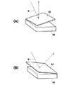
本発明者の研究によると、マイクロレンズで集光されたビームの集光位置における形状が歪んでしまうという前述の問題は、DMDを構成する微小ミラーの反射面の歪みに起因していることが判明した。従来、DMDにおいて画素部となる微小ミラーの反射面は、精度良く平坦に形成されているものと考えられて来たが、本発明者の分析によるとこの反射面はかなり歪んでおり、その歪みは、基本的に図18の(A)、(B)に示すような分布を有していることが分かった。以下、この歪みの分布について詳しく説明する。 According to the inventor's research, the above-mentioned problem that the shape of the beam condensed by the microlens is distorted is caused by the distortion of the reflection surface of the micromirror constituting the DMD. found. Conventionally, the reflection surface of a micromirror serving as a pixel portion in a DMD has been considered to be formed with high precision and flatness, but according to the analysis of the present inventors, this reflection surface is considerably distorted. It was found that basically has a distribution as shown in FIGS. 18 (A) and 18 (B). Hereinafter, this distortion distribution will be described in detail.
DMDを構成する矩形の微小ミラーは、その2つの対角線の一方と平行な揺動軸の周りに揺動するが、図18(A)はこの揺動軸と交わるx方向(揺動方向)の対角線に沿った断面内の歪分布を、そして同図(B)は上記揺動軸と平行なy方向(揺動軸方向)の対角線に沿った断面内の歪分布を示している。なおこれらの図において、横軸はミラー中心からの位置を示している。ここに示される通り、x方向ではミラー中心から±5100nm近辺の位置に歪みの変曲点が有り、一方、y方向ではミラー中心から±4500nm近辺の位置に歪みの変曲点が有り、それらの各変曲点よりもミラー中心側の領域では歪はなだらかに変化し、それよりも外側の領域では歪が比較的大きく変化している。
Rectangle micromirrors constituting the DMD are swung Suruga about one parallel to the oscillation axis of the two diagonals, Figure 18 (A) in the x-direction intersecting with the pivot shaft (swing direction) the strain distribution in cross section along the diagonal line, and FIG. (B) shows the strain distribution in the cross section along the diagonal line of the pivot shaft parallel to the y direction (the direction of the oscillation axis). In these drawings, the horizontal axis indicates the position from the mirror center. As shown here, there is an inflection point of distortion at a position near ± 5100 nm from the mirror center in the x direction, while there is an inflection point of distortion at a position near ± 4500 nm from the mirror center in the y direction. The distortion changes gently in the region on the mirror center side from each inflection point, and the distortion changes relatively greatly in the region outside it.
以上の知見に鑑みて本発明による画像露光装置においては、マイクロレンズアレイよりDMD側に離して、もしくは該マイクロレンズアレイと一体的にして、長軸を持つ細長い形状の開口を有する開口板が、矩形の微小ミラーの2つの対角線のうちミラー揺動軸と平行な対角線の方向、つまり上記y方向に開口短軸を対応させた状態で、各マイクロレンズ毎に設けられている。このような開口板が設けられていると、歪みの変化が比較的大きいミラー周辺部(すなわち上記変曲点よりも外側の部分)で反射した光の多くは開口板で遮断されるので、マイクロレンズで集光されたビームの集光位置における形状が歪んでしまうという問題を防止できる。
In view of the above knowledge, in the image exposure apparatus according to the present invention, an aperture plate having an elongated opening having a long axis, separated from the microlens array on the DMD side or integrally with the microlens array, Of the two diagonal lines of the rectangular micromirror, each microlens is provided in a state in which the short axis of opening corresponds to the direction of the diagonal line parallel to the mirror swing axis, that is, the y direction. When such an aperture plate is provided, most of the light reflected by the peripheral portion of the mirror (that is, the portion outside the inflection point) having a relatively large change in distortion is blocked by the aperture plate. The problem that the shape at the condensing position of the beam condensed by the lens is distorted can be prevented.
以上のようにして、マイクロレンズアレイの各マイクロレンズによって集光されたビームの集光位置における形状が歪んでしまうことを防止できれば、歪みの無い、より高精細な画像を露光可能となる。 As described above, if it is possible to prevent the shape of the beam collected by each microlens of the microlens array from being distorted, a higher-definition image without distortion can be exposed.
上記開口板による基本的な作用は、勿論開口の全周域に亘って得られるものであるが、本発明の画像露光装置において開口板は、微小ミラーの揺動軸と平行な対角線の方向に開口短軸をほぼ対応させた状態で配置されるので、この対角線方向およびその近辺については微小ミラーの中心から比較的短い範囲(ここは歪みの変化が比較的少ない領域である)で反射した光のみが開口を通過するようになり、ビーム形状の歪みを防止する効果がより確実なものとなる。その一方、上記とは別の対角線方向およびその近辺については、微小ミラーの中心から比較的長い範囲(ここも歪みの変化が比較的少なく、さらに歪自体も小さい領域である)で反射した光が開口を通過するようになるので、この方向において光を不必要に多く絞ることがなくなり、全体として光利用効率を高く保つことができる。
Of course, the basic action of the aperture plate can be obtained over the entire circumference of the aperture. However, in the image exposure apparatus of the present invention, the aperture plate is oriented in a diagonal direction parallel to the oscillation axis of the micromirror. Since it is arranged with the aperture short axis almost corresponding, light reflected in a relatively short range (this is a region with relatively little distortion change) from the center of the micromirror in this diagonal direction and its vicinity. Only passes through the opening, and the effect of preventing distortion of the beam shape is more certain. On the other hand, in the diagonal direction different from the above and in the vicinity thereof, light reflected in a relatively long range from the center of the micromirror (again, a region where the change in distortion is relatively small and the distortion itself is also small). Since the light passes through the opening, it is not necessary to squeeze an unnecessarily large amount of light in this direction, and the light utilization efficiency can be kept high as a whole.
なお、先に述べた特許文献2に示された構成において、消光比を高めることを目的として設置される開口板の開口径を全体的にある程度小さくすれば、マイクロレンズの集光位置におけるビーム形状の歪みを抑制する効果も得られる。しかしそのようにした場合は、開口板で遮断される光量がより多くなり、光利用効率が低下する。それに対して本発明の画像露光装置では光利用効率も高く保たれることは、先に述べた通りである。 In the configuration described in Patent Document 2 described above, if the aperture diameter of the aperture plate installed for the purpose of increasing the extinction ratio is reduced to some extent as a whole, the beam shape at the condensing position of the microlens The effect which suppresses distortion of this is also acquired. However, in such a case, the amount of light blocked by the aperture plate increases, and the light utilization efficiency decreases. On the other hand, as described above, the image exposure apparatus of the present invention also maintains high light utilization efficiency.
他方、本発明による画像露光方法は、上述した本発明による画像露光装置を用いて所定のパターンを感光材料に露光するものであるので、集光されたビームの集光位置における形状が歪んでしまうことを防止して、高精細なパターンを露光可能となる。 On the other hand, since the image exposure method according to the present invention exposes a predetermined pattern onto a photosensitive material using the image exposure apparatus according to the present invention described above, the shape of the condensed beam at the condensing position is distorted. This makes it possible to expose a high-definition pattern.
以下、図面を参照して、本発明の一実施形態による画像露光装置について説明する。 An image exposure apparatus according to an embodiment of the present invention will be described below with reference to the drawings.
[画像露光装置の構成]
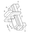
この画像露光装置は、図1に示すように、シート状の感光材料150を表面に吸着して保持する平板状の移動ステージ152を備えている。4本の脚部154に支持された厚い板状の設置台156の上面には、ステージ移動方向に沿って延びた2本のガイド158が設置されている。ステージ152は、その長手方向がステージ移動方向を向くように配置されると共に、ガイド158によって往復移動可能に支持されている。なお、この画像露光装置には、副走査手段としてのステージ152をガイド158に沿って駆動する後述のステージ駆動装置304(図15参照)が設けられている。
[Configuration of image exposure apparatus]
As shown in FIG. 1, the image exposure apparatus includes a flat plate-shaped moving
設置台156の中央部には、ステージ152の移動経路を跨ぐようにコ字状のゲート160が設けられている。コ字状のゲート160の端部の各々は、設置台156の両側面に固定されている。このゲート160を挟んで一方の側にはスキャナ162が設けられ、他方の側には感光材料150の先端および後端を検知する複数(例えば2個)のセンサ164が設けられている。スキャナ162およびセンサ164はゲート160に各々取り付けられて、ステージ152の移動経路の上方に固定配置されている。なお、スキャナ162およびセンサ164は、これらを制御する図示しないコントローラに接続されている。
A
スキャナ162は、図2および図3(B)に示すように、m行n列(例えば3行5列)の略マトリックス状に配列された複数(例えば14個)の露光ヘッド166を備えている。この例では、感光材料150の幅との関係で、3行目には4個の露光ヘッド166を配置してある。なお、m行目のn列目に配列された個々の露光ヘッドを示す場合は、露光ヘッド166mnと表記する。
As shown in FIGS. 2 and 3B, the
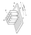
露光ヘッド166による露光エリア168は、副走査方向を短辺とする矩形状である。従って、ステージ152の移動に伴い、感光材料150には露光ヘッド166毎に帯状の露光済み領域170が形成される。なお、m行目のn列目に配列された個々の露光ヘッドによる露光エリアを示す場合は、露光エリア168mnと表記する。
An
また、図3(A)および(B)に示すように、帯状の露光済み領域170が副走査方向と直交する方向に隙間無く並ぶように、ライン状に配列された各行の露光ヘッドの各々は、配列方向に所定間隔(露光エリアの長辺の自然数倍、本例では2倍)ずらして配置されている。このため、1行目の露光エリア16811と露光エリア16812との間の露光できない部分は、2行目の露光エリア16821と3行目の露光エリア16831とにより露光することができる。
Further, as shown in FIGS. 3A and 3B, each of the exposure heads in each row arranged in a line so that the strip-shaped exposed
露光ヘッド16611〜166mnの各々は、図4および図5に示すように、入射された光ビームを画像データに応じて各画素毎に変調する空間光変調素子として、米国テキサス・インスツルメンツ社製のデジタル・マイクロミラー・デバイス(DMD)50を備えている。このDMD50は、データ処理部とミラー駆動制御部とを備えた後述のコントローラ302(図15参照)に接続されている。このコントローラ302のデータ処理部では、入力された画像データに基づいて、各露光ヘッド166毎にDMD50の制御すべき領域内の各マイクロミラーを駆動制御する制御信号を生成する。なお、制御すべき領域については後述する。また、ミラー駆動制御部では、画像データ処理部で生成した制御信号に基づいて、各露光ヘッド166毎にDMD50の各マイクロミラーの反射面の角度を制御する。なお、反射面の角度の制御については後述する。
As shown in FIGS. 4 and 5, each of the exposure heads 166 11 to 166 mn is manufactured by Texas Instruments, Inc. as a spatial light modulation element that modulates an incident light beam for each pixel according to image data. Digital micromirror device (DMD) 50. The
DMD50の光入射側には、光ファイバの出射端部(発光点)が露光エリア168の長辺方向と対応する方向に沿って一列に配列されたレーザ出射部を備えたファイバアレイ光源66、ファイバアレイ光源66から出射されたレーザ光を補正してDMD上に集光させるレンズ系67、このレンズ系67を透過したレーザ光をDMD50に向けて反射するミラー69がこの順に配置されている。なお図4では、レンズ系67を概略的に示してある。
On the light incident side of the
上記レンズ系67は、図5に詳しく示すように、ファイバアレイ光源66から出射した照明光としてのレーザ光Bを集光する集光レンズ71、この集光レンズ71を通過した光の光路に挿入されたロッド状オプティカルインテグレータ(以下、ロッドインテグレータという)72、およびこのロッドインテグレータ72の前方つまりミラー69側に配置された結像レンズ74から構成されている。集光レンズ71、ロッドインテグレータ72および結像レンズ74は、ファイバアレイ光源66から出射したレーザ光を、平行光に近くかつビーム断面内強度が均一化された光束としてDMD50に入射させる。このロッドインテグレータ72の形状や作用については、後に詳しく説明する。
As shown in detail in FIG. 5, the
上記レンズ系67から出射したレーザ光Bはミラー69で反射し、TIR(全反射)プリズム70を介してDMD50に照射される。なお図4では、このTIRプリズム70は省略してある。
The laser beam B emitted from the
またDMD50の光反射側には、DMD50で反射されたレーザ光Bを、感光材料150上に結像する結像光学系51が配置されている。この結像光学系51は図4では概略的に示してあるが、図5に詳細を示すように、レンズ系52,54からなる第1結像光学系と、レンズ系57,58からなる第2結像光学系と、これらの結像光学系の間に挿入されたマイクロレンズアレイ55と、アパーチャアレイ56とから構成されている。
On the light reflection side of the
マイクロレンズアレイ55は、DMD50の各画素に対応する多数のマイクロレンズ55aが2次元状に配列されてなるものである。本例では、後述するようにDMD50の1024個×768列のマイクロミラーのうち1024個×256列だけが駆動されるので、それに対応させてマイクロレンズ55aは1024個×256列配置されている。またマイクロレンズ55aの配置ピッチは縦方向、横方向とも41μmである。このマイクロレンズ55aは、一例として焦点距離が0.19mm、NA(開口数)が0.11で、光学ガラスBK7から形成されている。なおマイクロレンズ55aの形状については、後に詳しく説明する。そして、各マイクロレンズ55aの位置におけるレーザ光Bのビーム径は、41μmである。
The
また上記アパーチャアレイ56は、マイクロレンズアレイ55の各マイクロレンズ55aに対応する多数のアパーチャ(開口)56aが形成されてなるものであり、レンズ系54によるレーザ光Bの集光位置近傍に配置されている。なおこのアパーチャアレイ56については、後に詳しく説明する。
The
上記第1結像光学系は、DMD50による像を3倍に拡大してマイクロレンズアレイ55上に結像する。そして第2結像光学系は、マイクロレンズアレイ55を経た像を1.6倍に拡大して感光材料150上に結像、投影する。したがって全体では、DMD50による像が4.8倍に拡大して感光材料150上に結像、投影されることになる。
The first image-forming optical system forms an image on the
なお本例では、第2結像光学系と感光材料150との間にプリズムペア73が配設され、このプリズムペア73を図5中で上下方向に移動させることにより、感光材料150上における像のピントを調節可能となっている。なお同図中において、感光材料150は矢印F方向に副走査送りされる。
In this example, a
DMD50は図6に示すように、SRAMセル(メモリセル)60上に、各々画素(ピクセル)を構成する多数(例えば1024個×768個)の微小ミラー(マイクロミラー)62が格子状に配列されてなるミラーデバイスである。各ピクセルにおいて、最上部には支柱に支えられた矩形のマイクロミラー62が設けられており、マイクロミラー62の表面にはアルミニウム等の反射率の高い材料が蒸着されている。なお、マイクロミラー62の反射率は90%以上であり、その配列ピッチは縦方向、横方向とも一例として13.7μmである。また、マイクロミラー62の直下には、ヒンジおよびヨークを含む支柱を介して通常の半導体メモリの製造ラインで製造されるシリコンゲートのCMOSのSRAMセル60が配置されており、全体はモノリシックに構成されている。
As shown in FIG. 6, in the
DMD50のSRAMセル60にデジタル信号が書き込まれると、支柱に支えられたマイクロミラー62が、対角線を中心としてDMD50が配置された基板側に対して±α度(例えば±12度)の範囲で傾けられる。図7(A)は、マイクロミラー62がオン状態である+α度に傾いた状態を示し、図7(B)は、マイクロミラー62がオフ状態である−α度に傾いた状態を示す。したがって、画像信号に応じて、DMD50の各ピクセルにおけるマイクロミラー62の傾きを、図6に示すように制御することによって、DMD50に入射したレーザ光Bはそれぞれのマイクロミラー62の傾き方向へ反射される。
When a digital signal is written to the
なお図6には、DMD50の一部を拡大し、マイクロミラー62が+α度又は−α度に制御されている状態の一例を示す。それぞれのマイクロミラー62のオンオフ制御は、DMD50に接続された前記コントローラ302によって行われる。また、オフ状態のマイクロミラー62で反射したレーザ光Bが進行する方向には、光吸収体(図示せず)が配置されている。
FIG. 6 shows an example of a state in which a part of the
また、DMD50は、その短辺が副走査方向と所定角度θ(例えば、0.1°〜5°)を成すように僅かに傾斜させて配置するのが好ましい。図8(A)はDMD50を傾斜させない場合の各マイクロミラーによる反射光像(露光ビーム)53の走査軌跡を示し、図8(B)はDMD50を傾斜させた場合の露光ビーム53の走査軌跡を示している。
Further, it is preferable that the
DMD50には、長手方向にマイクロミラーが多数個(例えば1024個)配列されたマイクロミラー列が、短手方向に多数組(例えば756組)配列されているが、図8(B)に示すように、DMD50を傾斜させることにより、各マイクロミラーによる露光ビーム53の走査軌跡(走査線)のピッチP1が、DMD50を傾斜させない場合の走査線のピッチP2より狭くなり、解像度を大幅に向上させることができる。一方、DMD50の傾斜角は微小であるので、DMD50を傾斜させた場合の走査幅W2と、DMD50を傾斜させない場合の走査幅W1とは略同一である。
In the
また、異なるマイクロミラー列により同じ走査線上が重ねて露光(多重露光)されることになる。このように、多重露光されることで、アライメントマークに対する露光位置の微少量をコントロールすることができ、高精細な露光を実現することができる。また、主走査方向に配列された複数の露光ヘッドの間のつなぎ目を微少量の露光位置制御により段差無くつなぐことができる。 Further, the same scanning line is overlapped and exposed (multiple exposure) by different micromirror rows. Thus, by performing multiple exposure, it is possible to control a minute amount of the exposure position with respect to the alignment mark, and to realize high-definition exposure. Further, joints between a plurality of exposure heads arranged in the main scanning direction can be connected without a step by controlling a very small amount of exposure position.
なお、DMD50を傾斜させる代わりに、各マイクロミラー列を副走査方向と直交する方向に所定間隔ずらして千鳥状に配置しても、同様の効果を得ることができる。
Note that the same effect can be obtained by arranging the micromirror rows in a staggered manner by shifting the micromirror rows by a predetermined interval in the direction orthogonal to the sub-scanning direction instead of inclining the
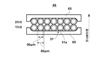
ファイバアレイ光源66は図9aに示すように、複数(例えば14個)のレーザモジュール64を備えており、各レーザモジュール64には、マルチモード光ファイバ30の一端が結合されている。マルチモード光ファイバ30の他端には、コア径がマルチモード光ファイバ30と同一で且つクラッド径がマルチモード光ファイバ30より小さい光ファイバ31が結合されている。図9bに詳しく示すように、マルチモード光ファイバ31の光ファイバ30と反対側の端部は副走査方向と直交する主走査方向に沿って7個並べられ、それが2列に配列されてレーザ出射部68が構成されている。
As shown in FIG. 9 a, the fiber
マルチモード光ファイバ31の端部で構成されるレーザ出射部68は、図9bに示すように、表面が平坦な2枚の支持板65に挟み込まれて固定されている。また、マルチモード光ファイバ31の光出射端面には、その保護のために、ガラス等の透明な保護板が配置されるのが望ましい。マルチモード光ファイバ31の光出射端面は、光密度が高いため集塵し易く劣化し易いが、上述のような保護板を配置することにより、端面への塵埃の付着を防止し、また劣化を遅らせることができる。
As shown in FIG. 9B, the
本例では図10に示すように、クラッド径が大きいマルチモード光ファイバ30のレーザ光出射側の先端部分に、長さ1〜30cm程度のクラッド径が小さい光ファイバ31が同軸的に結合されている。それらの光ファイバ30,31は、それぞれのコア軸が一致する状態で光ファイバ31の入射端面を光ファイバ30の出射端面に融着することにより結合されている。上述した通り、光ファイバ31のコア31aの径は、マルチモード光ファイバ30のコア30aの径と同じ大きさである。
In this example, as shown in FIG. 10, an
マルチモード光ファイバ30および光ファイバ31としては、ステップインデックス型光ファイバ、グレーテッドインデックス型光ファイバ、および複合型光ファイバの何れも適用可能である。例えば、三菱電線工業株式会社製のステップインデックス型光ファイバを用いることができる。本例において、マルチモード光ファイバ30および光ファイバ31はステップインデックス型光ファイバであり、マルチモード光ファイバ30は、クラッド径=125μm、コア径=50μm、NA=0.2、入射端面コートの透過率=99.5%以上であり、光ファイバ31は、クラッド径=60μm、コア径=50μm、NA=0.2である。
As the multimode
ただし、光ファイバ31のクラッド径は60μmには限定されない。従来のファイバ光源に使用されている多くの光ファイバのクラッド径は125μmであるが、クラッド径が小さくなるほど焦点深度がより深くなるので、マルチモード光ファイバのクラッド径は80μm以下が好ましく、60μm以下がより好ましい。一方、シングルモード光ファイバの場合、コア径は少なくとも3〜4μm必要であることから、光ファイバ31のクラッド径は10μm以上が好ましい。また、光ファイバ30のコア径と光ファイバ31のコア径を一致させることが、結合効率の点から好ましい。
However, the cladding diameter of the
レーザモジュール64は、図11に示す合波レーザ光源(ファイバ光源)によって構成されている。この合波レーザ光源は、ヒートブロック10上に配列固定された複数(例えば7個)のチップ状の横マルチモード又はシングルモードのGaN系半導体レーザLD1,LD2,LD3,LD4,LD5,LD6,およびLD7と、GaN系半導体レーザLD1〜LD7の各々に対応して設けられたコリメータレンズ11,12,13,14,15,16および17と、1つの集光レンズ20と、1本のマルチモード光ファイバ30とから構成されている。なお、半導体レーザの個数は7個に限定されるものではなく、その他の個数が採用されてもよい。また、上述のような7個のコリメータレンズ11〜17に代えて、それらのレンズが一体化されてなるコリメータレンズアレイを用いることもできる。
The
GaN系半導体レーザLD1〜LD7は、発振波長が総て共通(例えば、405nm)であり、最大出力も総て共通(例えばマルチモードレーザでは100mW、シングルモードレーザでは50mW程度)である。なお、GaN系半導体レーザLD1〜LD7としては、350nm〜450nmの波長範囲において、上記405nm以外の波長で発振するレーザを用いてもよい。 The GaN-based semiconductor lasers LD1 to LD7 all have a common oscillation wavelength (for example, 405 nm), and the maximum output is also all common (for example, about 100 mW for a multimode laser and about 50 mW for a single mode laser). As the GaN-based semiconductor lasers LD1 to LD7, lasers that oscillate at wavelengths other than 405 nm in the wavelength range of 350 nm to 450 nm may be used.
上記の合波レーザ光源は、図12および図13に示すように、他の光学要素と共に、上方が開口した箱状のパッケージ40内に収納されている。パッケージ40は、その開口を閉じるように作成されたパッケージ蓋41を備えており、脱気処理後に封止ガスを導入し、パッケージ40の開口をパッケージ蓋41で閉じることにより、それらによって形成される閉空間(封止空間)内に上記合波レーザ光源が気密封止されている。
As shown in FIGS. 12 and 13, the above combined laser light source is housed in a box-shaped
パッケージ40の底面にはベース板42が固定されており、このベース板42の上面には、前記ヒートブロック10と、集光レンズ20を保持する集光レンズホルダー45と、マルチモード光ファイバ30の入射端部を保持するファイバホルダー46とが取り付けられている。マルチモード光ファイバ30の出射端部は、パッケージ40の壁面に形成された開口からパッケージ外に引き出されている。
A
また、ヒートブロック10の側面にはコリメータレンズホルダー44が取り付けられており、そこにコリメータレンズ11〜17が保持されている。パッケージ40の横壁面には開口が形成され、この開口を通してGaN系半導体レーザLD1〜LD7に駆動電流を供給する配線47がパッケージ外に引き出されている。
A
なお、図13においては、図の煩雑化を避けるために、複数のGaN系半導体レーザのうちGaN系半導体レーザLD7にのみ番号を付し、複数のコリメータレンズのうちコリメータレンズ17にのみ番号を付している。
In FIG. 13, in order to avoid complication of the drawing, only the GaN semiconductor laser LD7 is numbered among the plurality of GaN semiconductor lasers, and only the
図14は、上記コリメータレンズ11〜17の取り付け部分の正面形状を示すものである。コリメータレンズ11〜17の各々は、非球面を備えた円形レンズの光軸を含む領域を平行な平面で細長く切り取った形状に形成されている。この細長形状のコリメータレンズは、例えば、樹脂又は光学ガラスをモールド成形することによって形成することができる。コリメータレンズ11〜17は、長さ方向がGaN系半導体レーザLD1〜LD7の発光点の配列方向(図14の左右方向)と直交するように、上記発光点の配列方向に密接配置されている。
FIG. 14 shows the front shape of the attachment part of the collimator lenses 11-17. Each of the
一方GaN系半導体レーザLD1〜LD7としては、発光幅が2μmの活性層を備え、活性層と平行な方向、直角な方向の拡がり角が各々例えば10°、30°の状態で各々レーザ光B1〜B7を発するレーザが用いられている。これらGaN系半導体レーザLD1〜LD7は、活性層と平行な方向に発光点が1列に並ぶように配設されている。 On the other hand, each of the GaN-based semiconductor lasers LD1 to LD7 includes an active layer having a light emission width of 2 μm, and the laser beams B1 to A laser emitting B7 is used. These GaN-based semiconductor lasers LD1 to LD7 are arranged so that the light emitting points are arranged in a line in a direction parallel to the active layer.
したがって、各発光点から発せられたレーザ光B1〜B7は、上述のように細長形状の各コリメータレンズ11〜17に対して、拡がり角度が大きい方向が長さ方向と一致し、拡がり角度が小さい方向が幅方向(長さ方向と直交する方向)と一致する状態で入射することになる。つまり、各コリメータレンズ11〜17の幅が1.1mm、長さが4.6mmであり、それらに入射するレーザ光B1〜B7の水平方向、垂直方向のビーム径は各々0.9mm、2.6mmである。また、コリメータレンズ11〜17の各々は、焦点距離f1=3mm、NA=0.6、レンズ配置ピッチ=1.25mmである。
Accordingly, in the laser beams B1 to B7 emitted from the respective light emitting points, the direction in which the divergence angle is large coincides with the length direction and the divergence angle is small with respect to the
集光レンズ20は、非球面を備えた円形レンズの光軸を含む領域を平行な平面で細長く切り取って、コリメータレンズ11〜17の配列方向、つまり水平方向に長く、それと直角な方向に短い形状に形成されている。この集光レンズ20は、焦点距離f2=23mm、NA=0.2である。この集光レンズ20も、例えば樹脂又は光学ガラスをモールド成形することにより形成される。
The condensing
次に図15を参照して、本例の画像露光装置における電気的な構成について説明する。ここに示されるように全体制御部300には変調回路301が接続され、該変調回路301にはDMD50を制御するコントローラ302が接続されている。また全体制御部300には、レーザモジュール64を駆動するLD駆動回路303が接続されている。さらにこの全体制御部300には、前記ステージ152を駆動するステージ駆動装置304が接続されている。
Next, the electrical configuration of the image exposure apparatus of this example will be described with reference to FIG. As shown here, a
[画像露光装置の動作]
次に、上記画像露光装置の動作について説明する。スキャナ162の各露光ヘッド166において、ファイバアレイ光源66の合波レーザ光源を構成するGaN系半導体レーザLD1〜LD7(図11参照)の各々から発散光状態で出射したレーザ光B1,B2,B3,B4,B5,B6,およびB7の各々は、対応するコリメータレンズ11〜17によって平行光化される。平行光化されたレーザ光B1〜B7は、集光レンズ20によって集光され、マルチモード光ファイバ30のコア30aの入射端面上で収束する。
[Operation of image exposure apparatus]
Next, the operation of the image exposure apparatus will be described. In each
本例では、コリメータレンズ11〜17および集光レンズ20によって集光光学系が構成され、その集光光学系とマルチモード光ファイバ30とによって合波光学系が構成されている。すなわち、集光レンズ20によって上述のように集光されたレーザ光B1〜B7が、このマルチモード光ファイバ30のコア30aに入射して光ファイバ内を伝搬し、1本のレーザ光Bに合波されてマルチモード光ファイバ30の出射端部に結合された光ファイバ31から出射する。
In this example, the
各レーザモジュールにおいて、レーザ光B1〜B7のマルチモード光ファイバ30への結合効率が0.9で、GaN系半導体レーザLD1〜LD7の各出力が50mWの場合には、アレイ状に配列された光ファイバ31の各々について、出力315mW(=50mW×0.9×7)の合波レーザ光Bを得ることができる。したがって、14本のマルチモード光ファイバ31全体では、4.4W(=0.315W×14)の出力のレーザ光Bが得られる。
In each laser module, when the coupling efficiency of the laser beams B1 to B7 to the multimode
画像露光に際しては、図15に示す変調回路301から露光パターンに応じた画像データがDMD50のコントローラ302に入力され、そのフレームメモリに一旦記憶される。この画像データは、画像を構成する各画素の濃度を2値(ドットの記録の有無)で表したデータである。
At the time of image exposure, image data corresponding to the exposure pattern is input from the
感光材料150を表面に吸着したステージ152は、図15に示すステージ駆動装置304により、ガイド158に沿ってゲート160の上流側から下流側に一定速度で移動される。ステージ152がゲート160下を通過する際に、ゲート160に取り付けられたセンサ164により感光材料150の先端が検出されると、フレームメモリに記憶された画像データが複数ライン分ずつ順次読み出され、データ処理部で読み出された画像データに基づいて各露光ヘッド166毎に制御信号が生成される。そして、ミラー駆動制御部により、生成された制御信号に基づいて各露光ヘッド166毎にDMD50のマイクロミラーの各々がオンオフ制御される。なお本例の場合、1画素部となる上記マイクロミラーのサイズは14μm×14μmである。
The
ファイバアレイ光源66からDMD50にレーザ光Bが照射されると、DMD50のマイクロミラーがオン状態のときに反射されたレーザ光は、レンズ系54、58により感光材料150上に結像される。このようにして、ファイバアレイ光源66から出射されたレーザ光が画素毎にオンオフされて、感光材料150がDMD50の使用画素数と略同数の画素単位(露光エリア168)で露光される。また、感光材料150がステージ152と共に一定速度で移動されることにより、感光材料150がスキャナ162によりステージ移動方向と反対の方向に副走査され、各露光ヘッド166毎に帯状の露光済み領域170が形成される。
When the
なお本例では、図16(A)および(B)に示すように、DMD50には、主走査方向にマイクロミラーが1024個配列されたマイクロミラー列が副走査方向に768組配列されているが、本例では、コントローラ302により一部のマイクロミラー列(例えば、1024個×256列)だけが駆動するように制御がなされる。
In this example, as shown in FIGS. 16A and 16B, the
この場合、図16(A)に示すようにDMD50の中央部に配置されたマイクロミラー列を使用してもよく、図16(B)に示すように、DMD50の端部に配置されたマイクロミラー列を使用してもよい。また、一部のマイクロミラーに欠陥が発生した場合は、欠陥が発生していないマイクロミラー列を使用するなど、状況に応じて使用するマイクロミラー列を適宜変更してもよい。
In this case, a micromirror array arranged at the center of the
DMD50のデータ処理速度には限界があり、使用する画素数に比例して1ライン当りの変調速度が決定されるので、一部のマイクロミラー列だけを使用することで1ライン当りの変調速度が速くなる。一方、連続的に露光ヘッドを露光面に対して相対移動させる露光方式の場合には、副走査方向の画素を全部使用する必要はない。
Since the data processing speed of the
スキャナ162による感光材料150の副走査が終了し、センサ164で感光材料150の後端が検出されると、ステージ152は、ステージ駆動装置304により、ガイド158に沿ってゲート160の最上流側にある原点に復帰し、再度、ガイド158に沿ってゲート160の上流側から下流側に一定速度で移動される。
When the sub-scanning of the
次に、図5に示したファイバアレイ光源66、集光レンズ71、ロッドインテグレータ72、結像レンズ74、ミラー69およびTIRプリズム70から構成されてDMD50に照明光としてのレーザ光Bを照射する照明光学系について説明する。ロッドインテグレータ72は例えば四角柱状に形成された透光性ロッドであり、その内部をレーザ光Bが全反射しながら進行するうちに、該レーザ光Bのビーム断面内強度分布が均一化される。なお、ロッドインテグレータ72の入射端面、出射端面には反射防止膜がコートされて、透過率が高められている。以上のようにして、照明光であるレーザ光Bのビーム断面内強度分布を高度に均一化できれば、照明光強度の不均一を無くして、高精細な画像を感光材料150に露光可能となる。
Next, the illumination comprising the fiber
ここで図17に、DMD50を構成するマイクロミラー62の反射面の平面度を測定した結果を示す。同図においては、反射面の同じ高さ位置を等高線で結んで示してあり、等高線のピッチは5nmである。なお同図に示すx方向およびy方向は、マイクロミラー62の2つ対角線方向であり、マイクロミラー62はy方向と平行に延びる揺動軸を中心として前述のように揺動する。また図18の(A)および(B)にはそれぞれ、上記x方向、y方向に沿ったマイクロミラー62の反射面の高さ位置変位を示す。
FIG. 17 shows the result of measuring the flatness of the reflecting surface of the
上記図17および図18に示される通り、マイクロミラー62の反射面には歪みが存在する。そして図18の(A)および(B)においてこの歪みの変化を精査すると、マイクロミラー62の揺動軸と交わるx方向ではミラー中心から±5100nm近辺の位置に歪みの変曲点が有り、上記揺動軸と平行なy方向ではミラー中心から±4500nm近辺の位置に歪みの変曲点が有り、それらの各変曲点よりもミラー中心側の領域では歪はなだらかに変化し、それよりも外側の領域では歪が比較的大きく変化している。また、y方向の歪みの変化は、x方向の歪みの変化と比べて著しく大きく、上記の傾向もより顕著となっている。マイクロミラー62の反射面に上述の歪みが存在すると、マイクロレンズアレイ55のマイクロレンズ55aで集光されたレーザ光Bの集光位置における形状が歪むという問題が発生し得る。なお図18の(A)に示される通り、上記反射面のx方向の歪みは、マイクロミラー62の中心に近い領域では比較的小さいものとなっている。
As shown in FIGS. 17 and 18, there is distortion on the reflecting surface of the
本実施形態の画像露光装置においては上述の問題に対処するために、先に述べたアパーチャアレイ56(図5参照)が設けられている。アパーチャアレイ56はその正面形状を図19に示す通り、多数の楕円形のアパーチャ56aが2次元状に並設されてなるものである。上記アパーチャ56aは、マイクロレンズアレイ55のマイクロレンズ55aと各々対応させて、該マイクロレンズ55aと同数設けられている。そしてアパーチャアレイ56は、その各アパーチャ56aがマイクロレンズ55aと光軸を一致させた状態となり、かつ楕円形のアパーチャ56aの短軸がマイクロミラー62の1つの対角線方向(y方向)と対応する状態に配設されている。ここで、「アパーチャ56aの短軸がマイクロミラー62のy方向と対応する」とは、アパーチャ56aとマイクロミラー62との光学的な位置関係において両者が揃うことを意味するものである。
In the image exposure apparatus of the present embodiment, the above-described aperture array 56 (see FIG. 5) is provided in order to cope with the above-described problem. As shown in FIG. 19, the
上述のようなアパーチャアレイ56が設けられていると、歪みの変化が比較的大きいマイクロミラー62の周辺部で反射したレーザ光Bの多くは該アパーチャアレイ56で遮断されるので、マイクロレンズ55aで集光されたレーザ光Bの集光位置における形状が歪んでしまうという問題を防止できる。そうであればレーザ光Bにより、歪みの無い、より高精細な画像を露光可能となる。
When the
上記アパーチャアレイ56による基本的な作用は、勿論アパーチャ56aの全周域に亘って得られるものであるが、本実施形態においてアパーチャアレイ56は、図19に示される通り、その短軸がマイクロミラー62の1つの対角線方向(y方向)と対応する状態に配設されているので、このy方向およびその近辺についてはマイクロミラー62の中心から比較的短い範囲(ここは歪みの変化が比較的少ない領域である)で反射したレーザ光Bのみがアパーチャ56aを通過するようになり、ビーム形状の歪みを防止する効果がより確実なものとなる。
Of course, the basic action of the
その一方、上記とは別の対角線方向、すなわち反射面の歪みの変化が小さい方の対角線方向(x方向)およびその近辺については、マイクロミラー62の中心から比較的長い範囲(ここも歪みの変化が比較的少なく、さらに歪自体も小さい領域である)で反射したレーザ光Bがアパーチャ56aを通過するようになるので、この方向において光を不必要に多く絞ることがなくなり、全体として光利用効率を高く保つことができる。このようにして光利用効率を高く確保できると、合波するレーザ光の本数を減らすことができ、よって余分な熱の発生も抑えることができる。
On the other hand, in the diagonal direction different from the above, that is, the diagonal direction (x direction) in which the change in distortion of the reflecting surface is smaller and the vicinity thereof, a relatively long range from the center of the micromirror 62 (again, the change in distortion) Since the laser beam B reflected by the relatively small amount of distortion and the distortion itself passes through the
なお、上記アパーチャ56aが、その短軸がマイクロミラー62のy方向と正確に対応する状態から、やや角度がずれた状態に配置されていても、基本的に上述の効果が得られることは勿論である。
Of course, even if the
また、本実施形態においてアパーチャアレイ56のアパーチャ56aは楕円形とされているが、図20に示す長円形のアパーチャ56bや、あるいは図21に示す細長い多角形状のアパーチャ56cを採用することも可能であり、そのようにした場合も、アパーチャ56aを楕円形とした場合と基本的に同様の効果を奏することができる。
Further, in the present embodiment, the
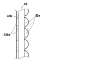
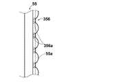
また本発明の画像露光装置において用いられる開口板は、上記実施形態におけるアパーチャアレイ56のようにマイクロレンズアレイ55と別体にして、それよりもDMD50側に配置する他、マイクロレンズアレイ55と一体的に形成されても構わない。図22および図23は、そのように形成された開口板の例を示すものである。図22に示す構成においては、マイクロレンズアレイ55のマイクロレンズ55aが形成された面と反対側(DMD側)の面に、細長い開口356aを有する遮光性マスク356が例えば蒸着等によって形成され、この遮光性マスク356が開口板として作用するようになっている。また図23に示す構成においては、マイクロレンズアレイ55のマイクロレンズ55aが形成された面に上記と同様の遮光性マスク356が形成され、この遮光性マスク356が開口板として作用するようになっている。
In addition, the aperture plate used in the image exposure apparatus of the present invention is separated from the
さらに、本発明の画像露光装置において開口板をマイクロレンズアレイと別体に形成する場合、その設置位置はDMDとマイクロレンズアレイとの間に限られるものではなく、DMDより光源側に開口板を設置してもよい。 Further, when the aperture plate is formed separately from the microlens array in the image exposure apparatus of the present invention, the installation position is not limited to between the DMD and the microlens array, and the aperture plate is disposed on the light source side from the DMD. May be installed.
LD1〜LD7 GaN系半導体レーザ
30、31 マルチモード光ファイバ
50 デジタル・マイクロミラー・デバイス(DMD)
51 拡大結像光学系
52、54 第1結像光学系のレンズ
55 マイクロレンズアレイ
56 アパーチャアレイ
56a、56b、56c アパーチャ(開口)
57、58 第2結像光学系のレンズ
66 レーザモジュール
66 ファイバアレイ光源
68 レーザ出射部
72 ロッドインテグレータ
150 感光材料
152 ステージ
162 スキャナ
166 露光ヘッド
168 露光エリア
170 露光済み領域
356 遮光性マスク
356a 遮光性マスクの開口
LD1-LD7 GaN semiconductor laser
30, 31 Multimode optical fiber
50 Digital micromirror device (DMD)
51 Magnification optical system
52, 54 Lens of the first imaging optical system
55 Micro lens array
56 Aperture array
56a, 56b, 56c Aperture (opening)
57, 58 Second imaging optical system lens
66 Laser module
66 Fiber array light source
68 Laser emission part
72 Rod integrator
150 photosensitive material
152 stages
162 Scanner
166 Exposure head
168 Exposure area
170 Exposed area
356 Shading Mask
356a Opening of shading mask
Claims (6)
このDMDに光を照射する光源と、
前記DMDの各微小ミラーからの光をそれぞれ集光するマイクロレンズがアレイ状に配されてなるマイクロレンズアレイを含み、前記DMDにより変調された光による像を感光材料上に結像する結像光学系とを備えた画像露光装置において、
前記マイクロレンズアレイよりDMD側に離して、もしくは該マイクロレンズアレイと一体的にして、短軸および長軸を持つ細長い形状の開口を有する開口板が、前記矩形の微小ミラーの2つの対角線のうちミラー揺動軸と平行な対角線の方向に開口短軸をほぼ対応させた状態で、各マイクロレンズ毎に設けられていることを特徴とする画像露光装置。
A plurality of oscillating rectangular micromirrors arranged two-dimensionally, DMD (digital micromirror device) that spatially modulates the incident light for each micromirror,
A light source for irradiating the DMD with light;
Imaging optics that includes a microlens array in which microlenses that collect light from each micromirror of the DMD are arranged in an array, and forms an image of light modulated by the DMD on a photosensitive material In an image exposure apparatus comprising a system,
An aperture plate having an elongated opening having a short axis and a long axis, separated from the microlens array on the DMD side or integrally with the microlens array, is one of the two diagonal lines of the rectangular micromirror. An image exposure apparatus provided for each microlens in a state in which a minor axis of an opening substantially corresponds to a diagonal direction parallel to a mirror swing axis.
Priority Applications (1)
| Application Number | Priority Date | Filing Date | Title |
|---|---|---|---|
| JP2004000395A JP4208141B2 (en) | 2004-01-05 | 2004-01-05 | Image exposure method and apparatus |
Applications Claiming Priority (1)
| Application Number | Priority Date | Filing Date | Title |
|---|---|---|---|
| JP2004000395A JP4208141B2 (en) | 2004-01-05 | 2004-01-05 | Image exposure method and apparatus |
Publications (3)
| Publication Number | Publication Date |
|---|---|
| JP2005195747A JP2005195747A (en) | 2005-07-21 |
| JP2005195747A5 JP2005195747A5 (en) | 2006-07-13 |
| JP4208141B2 true JP4208141B2 (en) | 2009-01-14 |
Family
ID=34816245
Family Applications (1)
| Application Number | Title | Priority Date | Filing Date |
|---|---|---|---|
| JP2004000395A Expired - Lifetime JP4208141B2 (en) | 2004-01-05 | 2004-01-05 | Image exposure method and apparatus |
Country Status (1)
| Country | Link |
|---|---|
| JP (1) | JP4208141B2 (en) |
Families Citing this family (3)
| Publication number | Priority date | Publication date | Assignee | Title |
|---|---|---|---|---|
| JP4588428B2 (en) * | 2004-12-09 | 2010-12-01 | 富士フイルム株式会社 | Image exposure method and apparatus |
| JP2006251748A (en) * | 2005-02-10 | 2006-09-21 | Fuji Photo Film Co Ltd | Image exposing device |
| JP5168659B2 (en) * | 2008-11-27 | 2013-03-21 | 株式会社リコー | Movable plate structure and optical scanning device |
-
2004
- 2004-01-05 JP JP2004000395A patent/JP4208141B2/en not_active Expired - Lifetime
Also Published As
| Publication number | Publication date |
|---|---|
| JP2005195747A (en) | 2005-07-21 |
Similar Documents
| Publication | Publication Date | Title |
|---|---|---|
| JP2005309380A (en) | Image exposure device | |
| JP4279053B2 (en) | Exposure head and exposure apparatus | |
| KR101140621B1 (en) | Image exposing method and apparatus | |
| KR100742251B1 (en) | Method and device for image exposure | |
| JP2003345030A (en) | Exposure device | |
| JP2007003829A (en) | Image exposure device | |
| JP2005032909A (en) | Lighting optical system and aligner using it | |
| TWI352879B (en) | Image exposure device | |
| JP2006195166A (en) | Image exposing device and microlens array unit | |
| JP2006337528A (en) | Image exposure system | |
| JP2005275325A (en) | Image exposing device | |
| JP4323335B2 (en) | Image exposure method and apparatus | |
| JP4208141B2 (en) | Image exposure method and apparatus | |
| JP4708785B2 (en) | Image exposure method and apparatus | |
| JP2004126034A (en) | Image forming apparatus | |
| JP2007004075A (en) | Image exposure apparatus | |
| KR100760253B1 (en) | Image exposure apparatus | |
| JP2006171426A (en) | Illumination optical system and exposure apparatus using the same | |
| JP4104949B2 (en) | Image forming apparatus | |
| JP2005217338A (en) | Image exposure method and apparatus | |
| JP2005049491A (en) | Illumination optical system | |
| JP2006258852A (en) | Structure for attaching microlens array, and image exposure device | |
| JP2006350011A (en) | Image exposure device | |
| JP2006267239A (en) | Mounting structure of digital micro-mirror device, and image exposure device | |
| JP2006337529A (en) | Image exposure system |
Legal Events
| Date | Code | Title | Description |
|---|---|---|---|
| A521 | Request for written amendment filed |
Free format text: JAPANESE INTERMEDIATE CODE: A523 Effective date: 20060518 |
|
| A621 | Written request for application examination |
Free format text: JAPANESE INTERMEDIATE CODE: A621 Effective date: 20060518 |
|
| A711 | Notification of change in applicant |
Free format text: JAPANESE INTERMEDIATE CODE: A712 Effective date: 20061206 |
|
| A977 | Report on retrieval |
Free format text: JAPANESE INTERMEDIATE CODE: A971007 Effective date: 20080729 |
|
| A131 | Notification of reasons for refusal |
Free format text: JAPANESE INTERMEDIATE CODE: A131 Effective date: 20080805 |
|
| A521 | Request for written amendment filed |
Free format text: JAPANESE INTERMEDIATE CODE: A523 Effective date: 20081001 |
|
| TRDD | Decision of grant or rejection written | ||
| A01 | Written decision to grant a patent or to grant a registration (utility model) |
Free format text: JAPANESE INTERMEDIATE CODE: A01 Effective date: 20081014 |
|
| A01 | Written decision to grant a patent or to grant a registration (utility model) |
Free format text: JAPANESE INTERMEDIATE CODE: A01 |
|
| A61 | First payment of annual fees (during grant procedure) |
Free format text: JAPANESE INTERMEDIATE CODE: A61 Effective date: 20081016 |
|
| R150 | Certificate of patent or registration of utility model |
Ref document number: 4208141 Country of ref document: JP Free format text: JAPANESE INTERMEDIATE CODE: R150 Free format text: JAPANESE INTERMEDIATE CODE: R150 |
|
| FPAY | Renewal fee payment (event date is renewal date of database) |
Free format text: PAYMENT UNTIL: 20111031 Year of fee payment: 3 |
|
| FPAY | Renewal fee payment (event date is renewal date of database) |
Free format text: PAYMENT UNTIL: 20121031 Year of fee payment: 4 |
|
| R250 | Receipt of annual fees |
Free format text: JAPANESE INTERMEDIATE CODE: R250 |
|
| FPAY | Renewal fee payment (event date is renewal date of database) |
Free format text: PAYMENT UNTIL: 20121031 Year of fee payment: 4 |
|
| FPAY | Renewal fee payment (event date is renewal date of database) |
Free format text: PAYMENT UNTIL: 20131031 Year of fee payment: 5 |
|
| R250 | Receipt of annual fees |
Free format text: JAPANESE INTERMEDIATE CODE: R250 |
|
| R250 | Receipt of annual fees |
Free format text: JAPANESE INTERMEDIATE CODE: R250 |
|
| S111 | Request for change of ownership or part of ownership |
Free format text: JAPANESE INTERMEDIATE CODE: R313113 |
|
| R350 | Written notification of registration of transfer |
Free format text: JAPANESE INTERMEDIATE CODE: R350 |
|
| R250 | Receipt of annual fees |
Free format text: JAPANESE INTERMEDIATE CODE: R250 |
|
| R250 | Receipt of annual fees |
Free format text: JAPANESE INTERMEDIATE CODE: R250 |
|
| R250 | Receipt of annual fees |
Free format text: JAPANESE INTERMEDIATE CODE: R250 |
|
| R250 | Receipt of annual fees |
Free format text: JAPANESE INTERMEDIATE CODE: R250 |
|
| R250 | Receipt of annual fees |
Free format text: JAPANESE INTERMEDIATE CODE: R250 |
|
| R250 | Receipt of annual fees |
Free format text: JAPANESE INTERMEDIATE CODE: R250 |
|
| R250 | Receipt of annual fees |
Free format text: JAPANESE INTERMEDIATE CODE: R250 |
|
| R250 | Receipt of annual fees |
Free format text: JAPANESE INTERMEDIATE CODE: R250 |
|
| R250 | Receipt of annual fees |
Free format text: JAPANESE INTERMEDIATE CODE: R250 |
|
| R250 | Receipt of annual fees |
Free format text: JAPANESE INTERMEDIATE CODE: R250 |
|
| EXPY | Cancellation because of completion of term |