JP2005292284A - Mounting structure, electro-optical device, and electronic apparatus - Google Patents
Mounting structure, electro-optical device, and electronic apparatus Download PDFInfo
- Publication number
- JP2005292284A JP2005292284A JP2004104309A JP2004104309A JP2005292284A JP 2005292284 A JP2005292284 A JP 2005292284A JP 2004104309 A JP2004104309 A JP 2004104309A JP 2004104309 A JP2004104309 A JP 2004104309A JP 2005292284 A JP2005292284 A JP 2005292284A
- Authority
- JP
- Japan
- Prior art keywords
- fpc
- flexible printed
- printed circuit
- electro
- circuit board
- Prior art date
- Legal status (The legal status is an assumption and is not a legal conclusion. Google has not performed a legal analysis and makes no representation as to the accuracy of the status listed.)
- Withdrawn
Links
- 239000000758 substrate Substances 0.000 description 20
- 239000004973 liquid crystal related substance Substances 0.000 description 17
- 239000010408 film Substances 0.000 description 5
- 238000000034 method Methods 0.000 description 5
- 238000005286 illumination Methods 0.000 description 4
- 238000005304 joining Methods 0.000 description 4
- 239000004372 Polyvinyl alcohol Substances 0.000 description 3
- 238000010586 diagram Methods 0.000 description 3
- 229920002451 polyvinyl alcohol Polymers 0.000 description 3
- ZCYVEMRRCGMTRW-UHFFFAOYSA-N 7553-56-2 Chemical compound [I] ZCYVEMRRCGMTRW-UHFFFAOYSA-N 0.000 description 2
- 238000002788 crimping Methods 0.000 description 2
- 238000009792 diffusion process Methods 0.000 description 2
- 238000005401 electroluminescence Methods 0.000 description 2
- 239000011521 glass Substances 0.000 description 2
- AMGQUBHHOARCQH-UHFFFAOYSA-N indium;oxotin Chemical compound [In].[Sn]=O AMGQUBHHOARCQH-UHFFFAOYSA-N 0.000 description 2
- 229910052740 iodine Inorganic materials 0.000 description 2
- 239000011630 iodine Substances 0.000 description 2
- 239000011159 matrix material Substances 0.000 description 2
- 239000004065 semiconductor Substances 0.000 description 2
- 239000010409 thin film Substances 0.000 description 2
- 239000000853 adhesive Substances 0.000 description 1
- 230000001070 adhesive effect Effects 0.000 description 1
- 230000001413 cellular effect Effects 0.000 description 1
- 239000001913 cellulose Substances 0.000 description 1
- 229920002678 cellulose Polymers 0.000 description 1
- 239000000470 constituent Substances 0.000 description 1
- 238000007689 inspection Methods 0.000 description 1
- 238000004519 manufacturing process Methods 0.000 description 1
- 229910052751 metal Inorganic materials 0.000 description 1
- 239000002184 metal Substances 0.000 description 1
- 230000003287 optical effect Effects 0.000 description 1
- 230000010287 polarization Effects 0.000 description 1
- 230000001681 protective effect Effects 0.000 description 1
- 239000011347 resin Substances 0.000 description 1
- 229920005989 resin Polymers 0.000 description 1
- 239000003566 sealing material Substances 0.000 description 1
- 125000006850 spacer group Chemical group 0.000 description 1
Images


Landscapes
- Liquid Crystal (AREA)
- Electroluminescent Light Sources (AREA)
- Structure Of Printed Boards (AREA)
- Combinations Of Printed Boards (AREA)
- Devices For Indicating Variable Information By Combining Individual Elements (AREA)
Abstract
Description
本発明は、実装構造体、電気光学装置、および電子機器に関し、詳細には、電気光学パネルに接続されるフレキシブルプリント基板を備えた実装構造体、電気光学装置、および電子機器に関する。 The present invention relates to a mounting structure, an electro-optical device, and an electronic device, and more particularly, to a mounting structure, an electro-optical device, and an electronic device that include a flexible printed board connected to an electro-optical panel.
一般に、液晶表示装置は、液晶表示パネルに液晶駆動用ICといった半導体素子を導電接続することによって作製される。かかる液晶表示パネルは、ガラスなどからなる一対の透明基板のそれぞれの表面上に所定パターンの透明電極を形成し、液晶を挟んでそれらの透明基板を互いに貼り合わせることによって形成される。液晶表示装置では、互いに対向する一対の透明電極によって画素が形成され、それらの透明電極に電圧の印加の有無によって画素の点灯/非点灯を行う。上記液晶表示パネルに駆動信号を供給するインターフェースとして、一般に、FPC(Flexible Printed Circuit)が使用される(例えば、特許文献1参照)。 In general, a liquid crystal display device is manufactured by conductively connecting a semiconductor element such as a liquid crystal driving IC to a liquid crystal display panel. Such a liquid crystal display panel is formed by forming transparent electrodes having a predetermined pattern on the surfaces of a pair of transparent substrates made of glass or the like, and bonding the transparent substrates to each other with a liquid crystal interposed therebetween. In a liquid crystal display device, a pixel is formed by a pair of transparent electrodes facing each other, and the pixel is turned on / off depending on whether a voltage is applied to the transparent electrode. Generally, an FPC (Flexible Printed Circuit) is used as an interface for supplying a driving signal to the liquid crystal display panel (see, for example, Patent Document 1).
上述のFPCは、FPCが搭載される電気光学装置や電子機器の仕様に応じて異なった形状や外形寸法が求められる場合が多い。これに対応するために、従来においては、電気光学装置や電子機器の仕様に合わせて、FPCを新たに設計して製造していたため、FPCの製造コストが高くなるという問題があった。 The above-described FPC often requires different shapes and outer dimensions depending on the specifications of the electro-optical device and electronic equipment on which the FPC is mounted. In order to cope with this, conventionally, since the FPC was newly designed and manufactured in accordance with the specifications of the electro-optical device and the electronic apparatus, there was a problem that the manufacturing cost of the FPC was increased.
本発明は、上記課題に鑑みてなされたものであり、フレキシブルプリント基板の形状や外形寸法を低コストで変更可能な実装構造体、電気光学装置、および電子機器を提供することを目的とする。 The present invention has been made in view of the above problems, and an object thereof is to provide a mounting structure, an electro-optical device, and an electronic apparatus that can change the shape and outer dimensions of a flexible printed circuit board at low cost.
上述した課題を解決し、目的を達成するために、本発明は、電気光学パネルにその一端側が接続され、電気部品を搭載する第1フレキシブルプリント基板と、その一端側が前記第1フレキシブルプリント基板の他端側と接続される第2フレキシブルプリント基板と、を備えたことを特徴とする。 In order to solve the above-described problems and achieve the object, the present invention provides a first flexible printed circuit board having one end connected to an electro-optical panel and mounting an electrical component, and one end of the first flexible printed circuit board. And a second flexible printed circuit board connected to the other end side.
これにより、第1フレキシブルプリント基板を汎用(共通)のフレキシブルプリント基板として使用し、低価格な第2フレキシブルプリント基板のみを交換することにより、要求される形状や外形寸法に変更することができる。この結果、フレキシブルプリント基板の形状や外形寸法を低コストで変更可能な実装構造体を提供することができる。 Accordingly, the first flexible printed board can be used as a general-purpose (common) flexible printed board, and only the low-cost second flexible printed board can be replaced to change to the required shape and outer dimensions. As a result, it is possible to provide a mounting structure that can change the shape and outer dimensions of the flexible printed circuit board at low cost.
また、本発明の好ましい態様によれば、前記第1フレキシブルプリント基板は、複数の接続位置で前記第2フレキシブルプリント基板を接続可能な入力接続部を有し、前記第2フレキシブルプリント基板は、前記第1フレキシブルプリント基板の入力接続部と接続する出力接続部を有し、前記入力接続部と前記出力接続部とが、前記複数の接続位置のうちの1つの接続位置で接続されていることが望ましい。これにより、同一の第2フレキシブルプリント基板を使用した場合においても、接続位置を変更することにより、外形寸法を簡単に変更することができる。 Further, according to a preferred aspect of the present invention, the first flexible printed board has an input connection portion capable of connecting the second flexible printed board at a plurality of connection positions, and the second flexible printed board is It has an output connection part connected with the input connection part of a 1st flexible printed circuit board, and the input connection part and the output connection part are connected at one connection position among the plurality of connection positions. desirable. Thereby, even when the same 2nd flexible printed circuit board is used, an external dimension can be changed easily by changing a connection position.
また、本発明の好ましい態様によれば、前記第1フレキシブルプリント基板には、前記入力接続部の前記複数の接続位置毎に、位置合わせ用の入力接続部アライメントマークが形成されており、前記第2フレキシブルプリント基板には、位置合わせ用の出力接続部アライメントマークが形成されており、前記入力接続部と前記出力接続部とが、前記入力接続部アライメントマークと前記出力接続部アライメントマークとを位置合わせすることにより、前記複数の接続位置のうちの1つの接続位置で接続されていることが望ましい。これにより、出力接続部アライメントマークと入力接続部アライメントマークを使用して、高精度に第1フレキシブルプリント基板の所望の位置に、第2フレキシブルプリント基板を接続することが可能となる。 According to a preferred aspect of the present invention, the first flexible printed board is provided with an input connection part alignment mark for alignment for each of the plurality of connection positions of the input connection part, 2 An output connection part alignment mark for alignment is formed on the flexible printed circuit board, and the input connection part and the output connection part position the input connection part alignment mark and the output connection part alignment mark. By combining them, it is desirable that the connection is made at one of the plurality of connection positions. Accordingly, it is possible to connect the second flexible printed circuit board to the desired position of the first flexible printed circuit board with high accuracy by using the output connection part alignment mark and the input connection part alignment mark.
また、本発明の好ましい態様によれば、前記第1フレキシブルプリント基板には、位置合わせ用の入力接続部穴が形成されており、前記第2フレキシブルプリント基板には、前記複数の接続位置に対応して複数の位置合わせ用の出力接続部穴が形成されており、前記入力接続部と前記出力接続部とが、前記位置合わせ用入力接続部穴と前記複数の位置合わせ用出力接続部穴のうちの1つ出力接続部穴とを位置合わせすることにより、前記複数の接続位置のうちの1つの接続位置で接続されていることが望ましい。これにより、位置合わせ用の出力接続部穴と位置合わせ用の入力接続部穴を使用して、高精度に第1フレキシブルプリント基板の所望の位置に、第2フレキシブルプリント基板を接続することが可能となる。 According to a preferred aspect of the present invention, the first flexible printed circuit board is formed with an input connection hole for alignment, and the second flexible printed circuit board corresponds to the plurality of connection positions. A plurality of alignment output connection holes are formed, and the input connection portion and the output connection portion are connected to the alignment input connection holes and the plurality of alignment output connection holes. It is desirable that one of the plurality of connection positions is connected by aligning one of the output connection holes. This makes it possible to connect the second flexible printed circuit board to the desired position of the first flexible printed circuit board with high accuracy using the output connecting hole for alignment and the input connection hole for alignment. It becomes.
また、本発明の好ましい態様によれば、本発明の実装構造体を電気光学装置に搭載することが望ましい。これにより、フレキシブルプリント基板の形状や外形寸法を低コストで変更可能な実装構造体を搭載した電気光学装置を提供することができる。 According to a preferred aspect of the present invention, it is desirable to mount the mounting structure of the present invention on an electro-optical device. Accordingly, it is possible to provide an electro-optical device equipped with a mounting structure that can change the shape and outer dimensions of the flexible printed circuit board at low cost.
また、本発明の好ましい態様によれば、本発明の電気光学装置を電子機器に搭載することが望ましい。これにより、フレキシブルプリント基板の形状や外形寸法を低コストで変更可能な実装構造体を搭載した電子機器を提供することができる。 According to a preferred aspect of the present invention, it is desirable to mount the electro-optical device of the present invention on an electronic apparatus. Thereby, the electronic device carrying the mounting structure which can change the shape and external dimension of a flexible printed circuit board at low cost can be provided.
以下、この発明につき図面を参照しつつ詳細に説明する。なお、この実施例によりこの発明が限定されるものではない。また、下記実施例における構成要素には、当業者が容易に想定できるものまたは実質的に同一のものが含まれる。本明細書において、電気光学装置とは、電気信号を光信号に変換する装置をいう。 Hereinafter, the present invention will be described in detail with reference to the drawings. Note that the present invention is not limited to the embodiments. In addition, constituent elements in the following embodiments include those that can be easily assumed by those skilled in the art or those that are substantially the same. In this specification, an electro-optical device refers to a device that converts an electrical signal into an optical signal.
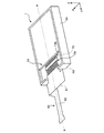
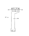
図1は本発明の実施例に係る電気光学装置1の構成例を示す図であり、図1−1は実施例に係る電気光学装置1の斜視図、図1−2は図1−1のA−A断面図を示している。 FIG. 1 is a diagram illustrating a configuration example of an electro-optical device 1 according to an embodiment of the present invention, FIG. 1-1 is a perspective view of the electro-optical device 1 according to the embodiment, and FIG. AA sectional drawing is shown.
図1に示すように、電気光学装置1は、画像を表示するための液晶表示パネル10と、液晶表示パネル10の上面側および下面側に貼付けられた第1偏光板20および第2偏光板30と、LED60の入射光を導光する導光板40と、導光板40から出射される光を表示面側に反射する反射板50と、光源であるLED60とを枠形状を呈する樹脂または金属からなるフレーム90内に収容して構成される。
As shown in FIG. 1, the electro-optical device 1 includes a liquid
第1基板10aおよび第2基板10bはガラス基板で構成されている。第1基板10aおよび第2基板10bは、不図示のスペーサによって所定のセルギャップを保持した状態でシール材11によって互いに接合される。こうして形成されたセルギャップ内に液晶14が封入される。
The
第1基板10aおよび第2基板10bの内表面には、ITO(Indium Tin Oxide:インジウムスズ酸化物)からなる透明電極12aおよび12bが形成され、これらの透明電極によって液晶表示のための画素が形成される。一方の第2基板10bは第1基板10aの外側に張り出す基板張出し部10b1を有しており、透明電極12aはその基板張出し部10b1上に形成された出力端子群13bに接続されている。また、基板張出し部10b1の端部には、入力端子群13aが形成されている。入力端子群13aおよび出力端子群13bは、透明電極12a、12bと同様にITO(Indium Tin Oxide:インジウムスズ酸化物)で形成されている。
また、基板張出し部10b1には、ドライバIC70が異方性導電膜(ACF:Anisotropic Conductive Film)でCOG実装されており、出力端子群13bと入力端子群13aとに接続されている。ACFの代わりに異方性導電接着剤を使用することにしても良い。また、入力端子群13aにおいては、FPC80の出力端子群と電気的に接続するように、ACFを介して接合されている。また、入力端子群13aの両側には、FPC80との接合の目印となる位置決め用のアライメントマーク(不図示)が設けられている。接合時には、このアライメントマークと、FPC80に設けられた位置決め用のアライメントマーク(不図示)を目標にして圧着接合されている。
Further, a
FPC(実装構造体)80は、メインFPC(第1フレキシブルプリント基板)81とI/F用FPC(第2フレキシブルプリント基板)82とで構成されている。メインFPC81の第2の面81bの端部とI/F用FPC82の第1の面82aの端部とがACFで接合されている。
The FPC (mounting structure) 80 includes a main FPC (first flexible printed circuit board) 81 and an I / F FPC (second flexible printed circuit board) 82. The end of the
第1基板10aおよび第2基板10bの背面側(光射出側およぼ光入射側)の面には、使用する液晶の種類、すなわち、TN(ツイステッドネマティック)モード、STN(スーパーTN)モード、D−STN(ダブル−STN)モード等々の動作モードや、ノーマリホワイトモード/ノーマリブラックモードの別に応じて、第1偏光板20および第2偏光板30が所定の向きに貼付配置される。
On the back side (light emitting side and light incident side) surfaces of the
第1偏光板20および第2偏光板30は、ポリビニルアルコール(PVA)フィルムを一方向に延伸し、ヨウ素または2色性色素を含む溶液に浸すことにより、ヨウ素または2色性色素を吸着させ、偏光機能を与え、更に保護膜としてセルロース系のフィルムを被覆して作製する。また、第1偏光板20および第2偏光板30の偏光方向は、PVAフィルムの延伸方向で決定される。
The first polarizing
第2偏光板30の下側には、導光板40が設けられている。導光板40は、その側方に配置されたLED60から発せられた照明光をその入射面(一端面)から入射して導光する。導光板40の下側には、導光板40から射出される照明光を表示面側に反射する反射板50が設けられている。導光板40の上側には、必要に応じて、導光板40から出射される照明光を拡散する拡散シートと、拡散シートで拡散された照明光を偏光するプリズムシートを設けることにしても良い。
A
上述したFPC80は、搭載される電子機器の仕様に応じて異なった形状や外形寸法が求められる場合が多い。そこで、本実施例では、FPC80をメインFPC81とI/F用FPC82に分割している。メインFPC81は、電気部品を搭載し液晶表示パネル10に接合されるもので共通化して使用される。I/F用FPC82は、搭載される電子機器の仕様に対応したもので、複数のパターンの中から選択される。
The FPC 80 described above often requires different shapes and outer dimensions depending on the specifications of the electronic device to be mounted. Therefore, in this embodiment, the FPC 80 is divided into a main FPC 81 and an I / F FPC 82. The main FPC 81 is mounted with electrical components and joined to the liquid
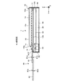
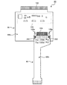
図2は、メインFPC81の構造を示す平面図であり、図2−1は図1のメインFPC81の第1の面81aの平面図、図2−2は、メインFPC81の第2の面81bの平面図を示している。
2 is a plan view showing the structure of the
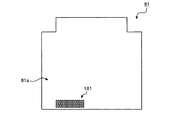
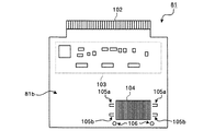
メインFPC81は、図2−1に示すように、第1の面81aに、導通検査を行うための検査用パット101を有している。また、メインFPC81は、図2−2に示すように、第2の面81bに、液晶表示パネル10と接続する出力端子群102と、電気部品が実装される電気部品実装領域103と、I/F用FPC82に接続する入力端子群(入力接続部)104と、入力端子群104の両端に設けられた2対のアライメントマーク(入力接続部アライメントマーク)105と、一対のアライメント穴(入力接続部穴)106とを有している。
As shown in FIG. 2A, the
I/F用FPC82に接続する入力端子群104の長さは、I/F用FPC82の出力端子群(図4参照)の長さよりも大きく形成されている。2対のアライメントマーク105は、入力端子群104の第1接続位置を規定する一対の第1アライメントマーク105aと、入力端子群104の第2接続位置を規定する第2アライメントマーク105bとからなる。このように、入力端子群104は、第1接続位置と第2接続位置で、I/F用FPC82の出力端子群と接続可能となっている。これにより、同一のI/F用FPC82を接続する場合においても、FPC80の外形寸法が2通りに変更可能となる。
The length of the
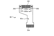
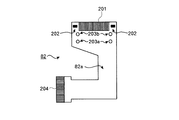
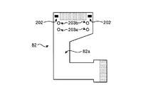
図3は、図1のI/F用FPC82の構造の一例を示す平面図であり、図3−1はI/F用FPC82の第1の面(表面)82aの平面図、図3−2はI/F用FPC82の第2の面(裏面)82bの平面図を示している。I/F用FPC82は、図3−1に示すように、第1の面82aに、メインFPC81と接続する出力端子群(出力接続部)201と、出力端子群201の両端に設けられた一対のアライメントマーク(出力接続部アライメントマーク)202と、一対のアライメントマーク202の後方に配された2対のアライメント穴(出力接続部穴)203と、メイン基板側(不図示)と接続する入力端子群204とを有している。2対のアライメント穴203は、メインFPC81の入力端子群104の第1接続位置で接続する場合に基準となる一対の第1アライメント穴203aと、第2接続位置で接続する場合に基準となる一対の第2アライメント穴203bとからなる。
3 is a plan view showing an example of the structure of the I /
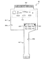
メインFPC81とI/F用FPC82の接合方法を図4を参照して説明する。図4は、メインFPC81とI/F用FPC82を接合する手順を説明するための工程図である。まず、メインFPC81の入力端子群104の所定位置にACFを貼り付ける(ACF貼付工程S1)。この後、メインFPC81の第2の面81bを表側にして、一対のアライメント穴106を、受け台(不図示)の一対の位置決めピンにセットして、受け台に対するメインFPC81の位置決めを行う(メインFPC位置決め工程S2)。
A method of joining the
つぎに、I/F用FPC82の第2の面82bを表側にして、一対の第1アライメント穴203aまたは一対の第2アライメント穴203bを受け台の同じ一対の位置決めピンにセットして、受け台に対するI/F用FPC82の位置決めを行う(I/F用FPC位置決め工程S3)。手動またはカメラユニットを使用して、メインFPC81の一対の第1アライメントマーク105aまたは一対の第2アライメントマーク105bと、I/F用FPC82のアライメントマーク202とを重ねて位置合わせを行なう(本位置決め工程S4)。
Next, set the pair of
ここで、メインFPC81の入力端子群104の第1位置にI/F用FPC82の出力端子群201を接合する場合には、I/F用FPC82の一対の第1アライメント穴203aを受け台の一対の位置決めピンにセットし、I/F用FPC82のアライメントマーク202をメインFPC81の一対の第1アライメントマーク105aに重ねる。他方、メインFPC81の入力端子群104の第2位置にI/F用FPC82の出力端子群201を接合する場合には、I/F用FPC82の一対の第2アライメント穴203bを受け台の一対の位置決めピンにセットし、I/F用FPC82のアライメントマーク202をメインFPC81の一対の第2アライメントマーク105bに重ねる。
Here, in the case where the
この後、不図示の圧着ヘッド(不図示)を下降させて、I/F用FPC82に対して所定の圧力で押圧して加熱圧着して、ACFでメインFPC81の入力端子群104とI/F用FPC82の出力端子群201とを導通接続する(圧着工程S5)。
Thereafter, a not-shown crimping head (not shown) is lowered, pressed against the I /
図5−1は、メインFPC81の入力端子群104の第1位置にI/F用FPC82の出力端子群201を接続したFPC80を示す平面図、図5−2は、メインFPC81の入力端子群104の第2位置にI/F用FPC82の出力端子群201を接続したFPC80を示す平面図である。図5に示すように、第1位置に接続した場合には、第2位置に接続した場合よりもFPC80の外形寸法が小さくなる。このように、メインFPC81に同一のI/F用FPC82を接続する場合においても、接続位置を2通りに変更することで、外形寸法の微調整を行うことができる。なお、本実施例では、I/F用FPCの接続位置を2通りに変更する構成を示したが、接続位置はこれに限られるものではなく、3通り以上に変更可能な構成としても良い。
5A is a plan view showing the
図6はI/F用FPC82の他の構成例1を示す平面図であり、図6−1はその第1の面82aの平面図、図6−2はその第2の面82bの平面図を示している。図7はI/F用FPC82の他の構成例2を示す平面図であり、図7−1はその第1の面82aの平面図、図7−2はその第2の面82bの平面図を示している。他の構成例1は、図6に示すように、I/F用FPC82の外形寸法を短くした構成である。他の構成例2は、図7に示すように、入力端子群204を側方に設けた構成である。上述したように、I/F用FPC82は、搭載される電子機器の仕様に対応させて、複数のパターンの中から選択される。本実施例においては、例えば、図4,図6,図7のI/F用FPC82の中から選択可能である。
6 is a plan view showing another configuration example 1 of the I /
以上説明したように、本実施例によれば、FPC80を液晶表示パネル10にその一端側が接続され、電気部品を搭載するメインFPC81と、その一端側がメインFPC81の他端側と接続されるI/F用FPC82とで構成しているので、メインFPC80を汎用(共通)のFPCとして使用し、低価格なI/F用FPCのみを交換することにより、要求される形状や外形寸法に変更することができる。
As described above, according to the present embodiment, the
また、本実施例によれば、メインFPC81は、複数の接続位置でI/F用FPC82を接続可能な構成であるので、同一のI/F用FPCを使用した場合においても、接続位置を変更することにより、外形寸法を簡単に変更することができる。
Further, according to the present embodiment, the
(電子機器への適用例)
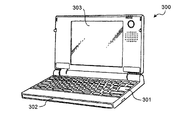
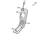
次に、本発明にかかる電気光学装置を適用可能な電子機器の具体例について図8を参照して説明する。図8−1は、本発明にかかる電気光学装置を可搬型のパーソナルコンピュータ(いわゆるノート型パソコン)300の表示部に適用した例を示す斜視図である。同図に示すように、パーソナルコンピュータ300は、キーボード301を備えた本体部302と、本発明にかかる電気光学装置を適用した表示部303とを備えている。図8−2は、本発明にかかる電気光学装置を携帯電話機400の表示部に適用した例を示す斜視図である。同図に示すように、携帯電話機400は、複数の操作ボタン401のほか、受話口402、送話口403とともに、本発明にかかる電気光学装置を適用した表示部404を備えている。
(Application example to electronic equipment)
Next, a specific example of an electronic apparatus to which the electro-optical device according to the invention can be applied will be described with reference to FIG. FIG. 8A is a perspective view illustrating an example in which the electro-optical device according to the present invention is applied to a display unit of a portable personal computer (so-called notebook personal computer) 300. As shown in the figure, a
本発明にかかる実装構造体は、半導体素子を基板に実装する各種装置に利用することができる。また、本発明にかかる電気光学装置は、透過型、反射型、および半透過型の電気光学装置に利用することができる。また、本発明にかかる電気光学装置は、パッシブマトリクス型の電気光学装置やアクティブマトリクス型の電気光学装置(例えば、TFT(薄膜トランジスタ)やTFD(薄膜ダイオード)をスイッチング素子として備えた電気光学パネル)に利用することができる。さらに、本発明にかかる電気光学装置は、液晶表示装置に限らず、有機エレクトロルミネッセンス装置、無機エレクトロルミネッセンス装置、プラズマディスプレイ装置、電気泳動表示装置、電子放出表示装置(Field Emission DisplayおよびSurface-Conduction Electoron-Emitter Display等)、LED(ライトエミッティングダイオード)表示装置等のように、複数の画素毎に表示状態を制御可能な各種の電気光学装置に利用することができる。 The mounting structure according to the present invention can be used in various devices for mounting a semiconductor element on a substrate. In addition, the electro-optical device according to the present invention can be used for a transmissive, reflective, and transflective electro-optical device. The electro-optical device according to the present invention is applied to a passive matrix type electro-optical device or an active matrix type electro-optical device (for example, an electro-optical panel including a TFT (thin film transistor) or a TFD (thin film diode) as a switching element). Can be used. Furthermore, the electro-optical device according to the present invention is not limited to a liquid crystal display device, but is an organic electroluminescence device, an inorganic electroluminescence device, a plasma display device, an electrophoretic display device, an electron emission display device (Field Emission Display and Surface-Conduction Electoron). -Emitter Display etc.), LED (Light Emitting Diode) display devices, etc., and can be used for various electro-optical devices that can control the display state for each of a plurality of pixels.
本発明にかかる電気光学装置を搭載した電子機器は、携帯電話機、PDA(Personal Digital Assistants)と呼ばれる携帯型情報機器、携帯型パーソナルコンピュータ、パーソナルコンピュータ、ワークステーション、デジタルスチルカメラ、車載用モニタ、デジタルビデオカメラ、液晶テレビ、ビューファインダ型、モニタ直視型のビデオテープレコーダ、カーナビゲーション装置、ページャ、電子手帳、電卓、ワードプロセッサ、ワークステーション、テレビ電話機、およびPOS端末機などの電子機器に広く利用することができる。 An electronic device equipped with the electro-optical device according to the present invention includes a mobile phone, a portable information device called PDA (Personal Digital Assistants), a portable personal computer, a personal computer, a workstation, a digital still camera, an in-vehicle monitor, a digital Widely used in electronic devices such as video cameras, LCD TVs, viewfinder type, monitor direct-view type video tape recorders, car navigation devices, pagers, electronic notebooks, calculators, word processors, workstations, video phones, and POS terminals. Can do.
1 電気光学装置、10 液晶表示パネル、10a 第1基板、10b 第2基板、20 第1偏光板、30 第2偏光板、40 導光板、50 反射板、60 LED、70 ドライバIC、80 FPC、81 メインFPC、82 I/F用FPC、101 検査用パット、102 出力端子群、103 電気部品実装領域、104 入力端子群、105a 第1アライメントマーク、105b 第2アライメントマーク、106 アライメント穴、201 出力端子群、202 アライメントマーク、203a 第1アライメント穴、203b 第2アライメント穴、300 パーソナルコンピュータ、301 キーボード、302 本体部、303 表示部、400 携帯電話機、401 操作ボタン、402 受話口、403 送話口、404 表示部
DESCRIPTION OF SYMBOLS 1 Electro-optical device, 10 Liquid crystal display panel, 10a 1st board | substrate, 10b 2nd board | substrate, 20 1st polarizing plate, 30 2nd polarizing plate, 40 Light guide plate, 50 Reflection plate, 60 LED, 70 Driver IC, 80 FPC, 81 main FPC, 82 I / F FPC, 101 inspection pad, 102 output terminal group, 103 electrical component mounting area, 104 input terminal group, 105a first alignment mark, 105b second alignment mark, 106 alignment hole, 201 output Terminal group, 202 Alignment mark, 203a First alignment hole, 203b Second alignment hole, 300 Personal computer, 301 Keyboard, 302 Main body, 303 Display unit, 400 Mobile phone, 401 Operation button, 402 Earpiece, 403
Claims (6)
その一端側が前記第1フレキシブルプリント基板の他端側と接続される第2フレキシブルプリント基板と、
を備えたことを特徴とする実装構造体。 A first flexible printed circuit board having one end connected to the electro-optic panel and mounting an electrical component;
A second flexible printed circuit board having one end connected to the other end of the first flexible printed circuit board;
A mounting structure characterized by comprising:
前記第2フレキシブルプリント基板は、前記第1フレキシブルプリント基板の入力接続部と接続する出力接続部を有し、
前記入力接続部と前記出力接続部とが、前記複数の接続位置のうちの1つの接続位置で接続されていることを特徴とする請求項1に記載の実装構造体。 The first flexible printed circuit board has an input connection portion capable of connecting the second flexible printed circuit board at a plurality of connection positions;
The second flexible printed circuit board has an output connection part connected to an input connection part of the first flexible printed circuit board,
The mounting structure according to claim 1, wherein the input connection portion and the output connection portion are connected at one connection position among the plurality of connection positions.
前記第2フレキシブルプリント基板には、位置合わせ用の出力接続部アライメントマークが形成されており、
前記入力接続部と前記出力接続部とが、前記入力接続部アライメントマークと前記出力接続部アライメントマークとを位置合わせすることにより、前記複数の接続位置のうちの1つの接続位置で接続されていることを特徴とする請求項2に記載の実装構造体。 On the first flexible printed board, an input connection part alignment mark for alignment is formed for each of the plurality of connection positions of the input connection part,
The second flexible printed circuit board has an output connection part alignment mark for alignment,
The input connection portion and the output connection portion are connected at one connection position among the plurality of connection positions by aligning the input connection portion alignment mark and the output connection portion alignment mark. The mounting structure according to claim 2.
前記第2フレキシブルプリント基板には、前記複数の接続位置に対応して複数の位置合わせ用の出力接続部穴が形成されており、前記入力接続部と前記出力接続部とが、前記位置合わせ用の入力接続部穴と前記複数の位置合わせ用の出力接続部穴のうちの1つ出力接続部穴とを位置合わせすることにより、前記複数の接続位置のうちの1つの接続位置で接続されていることを特徴とする請求項2に記載の実装構造体。 The first flexible printed circuit board has an input connection hole for alignment,
The second flexible printed circuit board has a plurality of alignment output connection holes corresponding to the plurality of connection positions, and the input connection portion and the output connection portion are used for the alignment. By aligning the input connection hole and the output connection hole of one of the plurality of alignment output connection holes, the input connection hole is connected at one of the plurality of connection positions. The mounting structure according to claim 2, wherein:
Priority Applications (1)
| Application Number | Priority Date | Filing Date | Title |
|---|---|---|---|
| JP2004104309A JP2005292284A (en) | 2004-03-31 | 2004-03-31 | Mounting structure, electro-optical device, and electronic apparatus |
Applications Claiming Priority (1)
| Application Number | Priority Date | Filing Date | Title |
|---|---|---|---|
| JP2004104309A JP2005292284A (en) | 2004-03-31 | 2004-03-31 | Mounting structure, electro-optical device, and electronic apparatus |
Publications (1)
| Publication Number | Publication Date |
|---|---|
| JP2005292284A true JP2005292284A (en) | 2005-10-20 |
Family
ID=35325308
Family Applications (1)
| Application Number | Title | Priority Date | Filing Date |
|---|---|---|---|
| JP2004104309A Withdrawn JP2005292284A (en) | 2004-03-31 | 2004-03-31 | Mounting structure, electro-optical device, and electronic apparatus |
Country Status (1)
| Country | Link |
|---|---|
| JP (1) | JP2005292284A (en) |
Cited By (8)
| Publication number | Priority date | Publication date | Assignee | Title |
|---|---|---|---|---|
| JP2007207782A (en) * | 2006-01-30 | 2007-08-16 | Fujikura Ltd | Composite flexible printed wiring board |
| JP2007250616A (en) * | 2006-03-14 | 2007-09-27 | Epson Imaging Devices Corp | Flexible circuit board, manufacturing method thereof, electro-optical apparatus, and electronic device |
| EP1925967A2 (en) | 2006-11-27 | 2008-05-28 | Funai Electric Co., Ltd. | Liquid crystal module |
| WO2011104934A1 (en) * | 2010-02-23 | 2011-09-01 | シャープ株式会社 | Display device |
| CN102200680A (en) * | 2010-03-23 | 2011-09-28 | 精工爱普生株式会社 | Substrate connection structure and projector |
| US8319109B2 (en) | 2008-04-03 | 2012-11-27 | Seiko Epson Corporation | Electro-optical device and electronic apparatus |
| JP2019003026A (en) * | 2017-06-15 | 2019-01-10 | 株式会社ジャパンディスプレイ | Display |
| JP2020016819A (en) * | 2018-07-27 | 2020-01-30 | セイコーエプソン株式会社 | Electro-optical devices and electronic equipment |
-
2004
- 2004-03-31 JP JP2004104309A patent/JP2005292284A/en not_active Withdrawn
Cited By (12)
| Publication number | Priority date | Publication date | Assignee | Title |
|---|---|---|---|---|
| JP2007207782A (en) * | 2006-01-30 | 2007-08-16 | Fujikura Ltd | Composite flexible printed wiring board |
| JP2007250616A (en) * | 2006-03-14 | 2007-09-27 | Epson Imaging Devices Corp | Flexible circuit board, manufacturing method thereof, electro-optical apparatus, and electronic device |
| EP1925967A2 (en) | 2006-11-27 | 2008-05-28 | Funai Electric Co., Ltd. | Liquid crystal module |
| US7728919B2 (en) | 2006-11-27 | 2010-06-01 | Funai Electric Co., Ltd. | Liquid crystal module having flexible printed wiring boards and a housing comprising multiple recesses to accommodate them |
| US8319109B2 (en) | 2008-04-03 | 2012-11-27 | Seiko Epson Corporation | Electro-optical device and electronic apparatus |
| WO2011104934A1 (en) * | 2010-02-23 | 2011-09-01 | シャープ株式会社 | Display device |
| CN102770894A (en) * | 2010-02-23 | 2012-11-07 | 夏普株式会社 | Display device |
| JP5173079B2 (en) * | 2010-02-23 | 2013-03-27 | シャープ株式会社 | Display device |
| CN102200680A (en) * | 2010-03-23 | 2011-09-28 | 精工爱普生株式会社 | Substrate connection structure and projector |
| CN102200680B (en) * | 2010-03-23 | 2013-12-11 | 精工爱普生株式会社 | Substrate connection structure and projector |
| JP2019003026A (en) * | 2017-06-15 | 2019-01-10 | 株式会社ジャパンディスプレイ | Display |
| JP2020016819A (en) * | 2018-07-27 | 2020-01-30 | セイコーエプソン株式会社 | Electro-optical devices and electronic equipment |
Similar Documents
| Publication | Publication Date | Title |
|---|---|---|
| CN101216618B (en) | Electro optical device and electronic apparatus | |
| US6211935B1 (en) | Alignment device for an IC-mounted structure | |
| TW583451B (en) | Electrooptic device, driving IC, and electronic apparatus | |
| US7580103B2 (en) | Electro-optical device, method of mounting wiring substrate, and electronic apparatus | |
| JP4367553B2 (en) | Electro-optical device and electronic apparatus | |
| US8563983B2 (en) | Display panel, display device, and method manufacturing same | |
| JP2005292284A (en) | Mounting structure, electro-optical device, and electronic apparatus | |
| JP2005266284A (en) | ELECTRO-OPTICAL DEVICE MANUFACTURING METHOD, ELECTRONIC DEVICE HAVING ELECTRO-OPTICAL DEVICE PRODUCED BY THE MANUFACTURING METHOD, AND POLARIZER | |
| JP2006235503A (en) | Display device | |
| JP2005277160A (en) | Mounting structure manufacturing method, mounting structure, electro-optical device, and electronic apparatus | |
| JP3760973B2 (en) | ELECTRO-OPTICAL DEVICE, ITS MANUFACTURING METHOD, AND ELECTRONIC DEVICE | |
| JP2006284978A (en) | Electrooptical device and electronic apparatus | |
| JP4572323B2 (en) | Electro-optical device and electronic apparatus | |
| JP2005283829A (en) | Electro-optical device and electronic apparatus | |
| JP2009031618A (en) | Liquid crystal device and electronic apparatus | |
| JP4296877B2 (en) | Electro-optical device and electronic apparatus including the electro-optical device | |
| JP2004152984A (en) | Wiring board, electro-optical device and electronic equipment | |
| JP2008009038A (en) | Liquid crystal device, lighting device and electronic apparatus | |
| JP2002323865A (en) | Electro-optical devices and electronic equipment | |
| JP2008209792A (en) | Liquid crystal display device | |
| JP4470793B2 (en) | Electro-optical device and electronic apparatus | |
| JP2008185801A (en) | Electro-optical device manufacturing method, electro-optical device, and electronic apparatus | |
| JP2005266110A (en) | Backlight unit, electro-optical device, and electronic device | |
| JP3911931B2 (en) | Liquid crystal device, method for manufacturing liquid crystal device, and electronic apparatus | |
| JP2005108997A (en) | Semiconductor element mounting method, electro-optical device manufacturing method, electro-optical device, and electronic apparatus equipped with the electro-optical device |
Legal Events
| Date | Code | Title | Description |
|---|---|---|---|
| A300 | Application deemed to be withdrawn because no request for examination was validly filed |
Free format text: JAPANESE INTERMEDIATE CODE: A300 Effective date: 20070605 |