JP2005292013A - Surface analyzer - Google Patents
Surface analyzer Download PDFInfo
- Publication number
- JP2005292013A JP2005292013A JP2004109567A JP2004109567A JP2005292013A JP 2005292013 A JP2005292013 A JP 2005292013A JP 2004109567 A JP2004109567 A JP 2004109567A JP 2004109567 A JP2004109567 A JP 2004109567A JP 2005292013 A JP2005292013 A JP 2005292013A
- Authority
- JP
- Japan
- Prior art keywords
- sample
- lens
- electron
- charged particles
- secondary charged
- Prior art date
- Legal status (The legal status is an assumption and is not a legal conclusion. Google has not performed a legal analysis and makes no representation as to the accuracy of the status listed.)
- Pending
Links
Images
Landscapes
- Analysing Materials By The Use Of Radiation (AREA)
Abstract
【課題】 本発明が解決しようとする問題点は、磁場型結像レンズを使用する分析モードでは電気導電性のない試料を分析することが困難であるという点である。
【解決手段】 試料を磁場中に浸漬する磁場レンズと、前記試料を励起して2次荷電粒子を発生させる励起線源と、前記2次荷電粒子を捕集する捕集レンズと、前記捕集レンズで捕集した前記2次荷電粒子を検出するアナライザと、前記2次荷電粒子が発生した前記試料を電子により中和する電子供給源と、前記電子供給源から供給された前記電子を前記試料へ加速する電子加速手段と、を備えた荷電粒子エネルギー分析装置であって、前記捕集レンズと前記試料との間に前記2次荷電粒子を前記捕集レンズに向けて通過させる開口を有する接地電極を設け、前記電子供給源を前記接地電極内に配置するようにした荷電粒子エネルギー分析装置。
【選択図】 図2
PROBLEM TO BE SOLVED: The problem to be solved by the present invention is that it is difficult to analyze a sample having no electrical conductivity in an analysis mode using a magnetic imaging lens.
A magnetic lens that immerses a sample in a magnetic field, an excitation source that excites the sample to generate secondary charged particles, a collection lens that collects the secondary charged particles, and the collection An analyzer for detecting the secondary charged particles collected by the lens; an electron supply source for neutralizing the sample in which the secondary charged particles are generated; and the sample supplied from the electron supply source. An electron acceleration means for accelerating to the ground, and a grounding device having an opening for passing the secondary charged particles toward the collection lens between the collection lens and the sample A charged particle energy analyzer comprising an electrode and the electron supply source disposed in the ground electrode.
[Selection] Figure 2
Description
本発明は光電子分光装置等の表面分析装置に関する。 The present invention relates to a surface analyzer such as a photoelectron spectrometer.
光電子分光装置は、X線を試料表面に照射し、試料から放出された光電子をインプットレンズ、エネルギーアナライザ等から構成される電子分光器でエネルギー測定することにより、試料表面に存在する元素の同定、化学結合状態および構造解析等の分析を行う装置である。 The photoelectron spectrometer irradiates the sample surface with X-rays, and measures the energy of the photoelectrons emitted from the sample with an electron spectrometer composed of an input lens, an energy analyzer, etc., thereby identifying the elements present on the sample surface. It is an apparatus that performs analysis such as chemical bonding state and structural analysis.
光電子分光装置において磁場型の電磁レンズを利用して特定の問題箇所を限定し、電気導電性のない試料を分析する場合、電気導電性のない試料は光電子を発生させるための手段として軟X線や真空紫外光を照射すると光電子及びオージェ電子などの2次電子が試料表面から真空中へ放出された結果、試料表面が正に帯電する。試料表面が正に帯電すると試料表面から光電子が放出される際に、帯電による電界の影響で光電子の運動エネルギーが減速され、この結果観察されるスペクトルはエネルギー値がシフトして観察される。試料表面の状況によっては観察されるピークのエネルギー値がシフトするばかりでなく、局所帯電の影響で正確なピーク形状の観察が行えない。そして、正確なピーク形状を得られないためにピークを幾つかの成分に分離して行う化学状態分析の解析結果に重大な悪影響を及ぼす場合がある。 When analyzing a non-electrically conductive sample using a magnetic field type electromagnetic lens in a photoelectron spectrometer to analyze a non-electrically conductive sample, the non-electrically conductive sample is a soft X-ray as a means for generating photoelectrons. When irradiated with vacuum ultraviolet light, secondary electrons such as photoelectrons and Auger electrons are emitted from the sample surface into the vacuum, and as a result, the sample surface is positively charged. When the sample surface is positively charged, when photoelectrons are emitted from the sample surface, the kinetic energy of the photoelectrons is decelerated due to the influence of the electric field due to the charge, and as a result, the observed spectrum is observed with the energy value shifted. Depending on the condition of the sample surface, not only the observed peak energy value is shifted, but also the accurate peak shape cannot be observed due to the influence of local charging. In addition, since an accurate peak shape cannot be obtained, the analysis result of the chemical state analysis performed by separating the peak into several components may be seriously adversely affected.
この場合、分析室のインプットレンズを取り付けた位置と異なるポートに低エネルギーの電子線を発生する帯電補償電子銃を取り付け、この帯電補償電子銃から供給される低速エネルギー電子を用いて試料表面の電位補償を行っていた。 In this case, a charge-compensating electron gun that generates a low-energy electron beam is attached to a port different from the position where the input lens of the analysis room is attached, and the potential of the sample surface is determined using low-energy electrons supplied from the charge-compensating electron gun. I had compensation.
なお、従来技術としては、磁場型結像レンズを備えた電子分光装置がある(例えば、特許文献1)。 In addition, as a prior art, there exists an electron spectroscopy apparatus provided with the magnetic field type | mold imaging lens (for example, patent document 1).
しかしながら、この磁場型結像レンズによって試料の周りに生成される磁場によって、帯電補償電子銃より磁場の磁界線に対して斜め方向から供給される低エネルギーの電子は試料の分析位置に到達できない。 However, due to the magnetic field generated around the sample by the magnetic field type imaging lens, the low energy electrons supplied from the oblique direction with respect to the magnetic field line of the magnetic field from the charge compensating electron gun cannot reach the analysis position of the sample.
本発明が解決しようとする問題は、磁場型結像レンズを使用する分析モードでは電気導電性のない試料を分析することが困難であるという点である。 The problem to be solved by the present invention is that it is difficult to analyze a sample having no electrical conductivity in the analysis mode using the magnetic field type imaging lens.
請求項1の発明は、試料を磁場中に浸漬する磁場レンズと、前記試料を励起して2次荷電粒子を発生させる励起線源と、前記2次荷電粒子を捕集する捕集レンズと、前記捕集レンズで捕集した前記2次荷電粒子を検出するアナライザと、前記2次荷電粒子が発生した前記試料を電子により中和する電子供給源と、前記電子供給源から供給された前記電子を前記試料へ加速する電子加速手段と、を備えた荷電粒子エネルギー分析装置であって、前記捕集レンズと前記試料との間に前記2次荷電粒子を前記捕集レンズに向けて通過させる開口を有する接地電極を設け、前記電子供給源を前記接地電極内に配置するようにした荷電粒子エネルギー分析装置である。 The invention of claim 1 includes a magnetic lens that immerses a sample in a magnetic field, an excitation source that excites the sample to generate secondary charged particles, a collection lens that collects the secondary charged particles, An analyzer for detecting the secondary charged particles collected by the collection lens, an electron supply source for neutralizing the sample in which the secondary charged particles are generated with electrons, and the electrons supplied from the electron supply source An electron acceleration means for accelerating the sample to the sample, and an aperture through which the secondary charged particles pass between the collection lens and the sample toward the collection lens The charged particle energy analyzer is provided with a ground electrode having a structure in which the electron supply source is disposed in the ground electrode.
請求項2の発明は、前記電子供給源が環状のフィラメントである請求項1に記載した荷電粒子エネルギー分析装置である。
The invention of
請求項3の発明は、前記電子加速手段を制御する電子加速制御手段を備えた請求項1又は2に記載した荷電粒子エネルギー分析装置であって、前記電子加速制御手段は前記2次荷電粒子の測定前に前記電子供給源から前記試料へ前記電子を加速し、前記2次荷電粒子の測定中は前記電子供給源からの前記電子を加速しないように制御する荷電粒子エネルギー分析装置である。
The invention according to claim 3 is the charged particle energy analyzer according to
請求項4の発明は、前記2次荷電粒子が光電子である請求項1乃至3のいずれかに記載された荷電粒子エネルギー分析装置である。 A fourth aspect of the present invention is the charged particle energy analyzer according to any one of the first to third aspects, wherein the secondary charged particles are photoelectrons.
本発明により、磁場型結像レンズを使用する分析モードでも、帯電した電気導電性のない試料に電子を供給して補償させることができる。 According to the present invention, even in an analysis mode using a magnetic imaging lens, it is possible to compensate by supplying electrons to a charged non-conductive sample.
以下、図面を用いて本発明の実施の形態について説明する。 Hereinafter, embodiments of the present invention will be described with reference to the drawings.
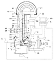
図1は、本発明の電子分光装置の一例を示したものであり、光電子分光装置の断面図である。 FIG. 1 shows an example of an electron spectrometer of the present invention, and is a cross-sectional view of a photoelectron spectrometer.
まず、図1の装置構成について説明すると、1は分析室チャンバである。分析室チャンバ1の内部の分析室2は、排気装置3により超高真空に排気されている。分析室2の真空度は真空ゲージ4でモニタされており、真空ゲージ4の検出出力は制御装置5に供給されている。
First, the apparatus configuration of FIG. 1 will be described. Reference numeral 1 denotes an analysis chamber. The
6は光電子励起X線源(照射手段)であり、X線源6は分析室チャンバ1のポートに取り付けられている。このX線源6は、分析室2に配置された試料7にX線(1次線)を照射して、光電子を励起するための励起光源である。X線源6は、X線源電源8を介して制御装置5に接続されている。
Reference numeral 6 denotes a photoelectron excitation X-ray source (irradiation means), and the X-ray source 6 is attached to a port of the analysis chamber 1. The X-ray source 6 is an excitation light source for irradiating a
試料7は試料ホルダ9に保持されていて、試料ホルダ9は試料ステージ10上に置かれている。試料ステージ10は分析室チャンバ1に取り付けられており、試料ステージ位置調整機構11を調整することによって、試料ステージ10をx,yおよびz方向に移動させることができる。
The
14は磁界型結像レンズであり、磁界型結像レンズ14は試料7の下方に配置されている。この磁界型結像レンズ14は試料ステージ10に取り付けられている。
また、図1において、19は電子分光器であり、電子分光器19は分析室チャンバ1に取り付けられている。この電子分光器19は、インプットレンズ20と、インプットレンズ20からの電子をエネルギー分析するためのアナライザ21と、アナライザ21で選別された電子を検出する検出器22で構成されている。
In FIG. 1, 19 is an electron spectrometer, and the
筒状のインプットレンズ20は、試料側から順に、筒状の接地電極23、筒状の電極(主倍率制御レンズL1)34、筒状の接地電極24、筒状の電極(補助倍率制御レンズL2)35、筒状の接地電極25、筒状の電極(結像レンズL3)36、筒状の接地電極26、筒状の電極(減速レンズLR)37を備えている。なお、これらの各電極は、隣の電極と所定の間隔を置いて配置されている。
The
また、インプットレンズ20は円形の視野制限絞り27を有している。この視野制限絞り27は、補助倍率制御レンズ35と結像レンズ36間に、インプットレンズ20の筒内を仕切るように配置されている。視野制限絞り27の開口aの中心は、インプットレンズ20の光軸O上に位置している。
The
そして、視野制限絞り27は虹彩絞りが用いられており、開口径調整機構28を調整することによって、視野制限絞り27の開口径を連続して変えることができる。このため、視野制限絞り27が完全に閉じられると、その左右のインプットレンズ内の空間は、絞り27によって真空的に完全に遮断される。なお、視野制限絞り27は、試料7面上で発生した光電子を取り込む領域を制限するために設けられており、この絞りによって、試料7上の分析領域の大きさを設定することができる。
An iris diaphragm is used as the
さらに、インプットレンズ20は円形の角度制限絞り29を有している。この角度制限絞り29は、視野制限絞り27と結像レンズ36間に、インプットレンズ20の筒内を仕切るように配置されている。角度制限絞り29の開口bの中心は、インプットレンズ20の光軸O上に位置している。
Further, the
そして、角度制限絞り29も虹彩絞りが用いられており、開口径調整機構30を調整することによって、角度制限絞り29の開口径を連続して変えることができる。このため、角度制限絞り29が完全に閉じられると、その左右のインプットレンズ内の空間は、絞り29によって真空的に完全に遮断される。なお、角度制限絞り29は、視野制限絞り27を通過した光電子の取込角度を制限するために設けられており、この角度制限絞りによって、レンズ系の球面収差によるボケを低減し、試料上の分析領域の精度を保証することができる。
An iris diaphragm is also used as the
なお、図1のインプットレンズ20においては、主倍率制御レンズ34と補助倍率制御レンズ35で本発明の第1レンズが構成されており、結像レンズ36と減速レンズ37で本発明の第2レンズが構成されている。
In the
また、図1において、31はアナライザ21の入射スリット、32は電源ユニットである。この電源ユニット32は、電子分光器19の各構成要素に印加する電圧と、磁界型結像レンズ14のコイルに流れる電流とを制御するためのものである。
In FIG. 1, 31 is an entrance slit of the
そして、制御装置5は、電源ユニット32、検出器22および表示装置33に接続されている。
The control device 5 is connected to the
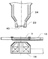
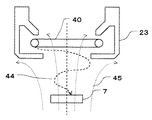
図2は、図1におけるインプットレンズ20下端部分の断面詳細図である。インプットレンズ下端には接地電極23が接地されている。接地電極23内部には帯電補償電子源40が収納されている。
2 is a detailed cross-sectional view of the lower end portion of the
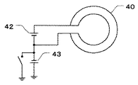
図3は、図2における帯電補償電子源40の平面図である。環状の熱フィラメントより構成されている帯電補償電子源40には、加熱電源42及び放出された電子を試料に加速させる加速電源43が接続されている。
FIG. 3 is a plan view of the charge compensating
以上、図における各部の構成について説明したが、次に動作について説明する。 The configuration of each unit in the figure has been described above. Next, the operation will be described.
図1において、分析室2の真空度は制御装置5で常に監視されており、制御装置5は真空度適正であると、試料7にX線照射を行うためのX線照射信号をX線源電源8に送る。また、制御装置5は、電子分光器19の各構成要素に所定の電圧を印加するための電圧制御信号を電源ユニット32に供給する。
In FIG. 1, the degree of vacuum in the
X線照射信号を受けたX線源電源8は、そのX線照射信号に基づいてX線源6を制御する。この結果、X線源6からX線が発生し、試料7にX線が照射される。
The X-ray source power supply 8 that has received the X-ray irradiation signal controls the X-ray source 6 based on the X-ray irradiation signal. As a result, X-rays are generated from the X-ray source 6 and the
一方、電圧制御信号を受けた電源ユニット32は、その電圧制御信号に基づいて電子分光器19を制御する。微小領域分析を感度良く行うために磁場型結像レンズを使用する場合、電源ユニット32は、X線照射によって試料7のX線照射領域から発生した光電子が視野制限絞り27上に結像するように、磁界型結像レンズ14のコイルに電流を供給すると共に、補助倍率制御レンズ35に電圧V2を印加する。
On the other hand, the
また、電源ユニット32は、視野制限絞り27と角度制限絞り29を通過した光電子が減速するように、減速レンズ37に電圧VRを印加する。電源ユニット32は、視野制限絞り27と角度制限絞り29を通過して減速レンズ37で減速された光電子が、入射スリット31上に結像するように、結像レンズ36に電圧V3を印加する。さらに、電源ユニット32は、アナライザ21と検出器22に所定の電圧を印加する。
The
なお、磁場型結像レンズ14と補助倍率制御レンズ35の2段レンズで構成されているので、この磁場型結像レンズ14と補助倍率制御レンズ35に印加する電圧を変更すれば、そのレンズ倍率を変更することができる。その際、光電子が視野制限絞り27上に常に結像するように、磁場型結像レンズ14と補助倍率制御レンズ35に印加する電圧の組み合わせが変更される。この場合は、主倍率制御レンズ34には、電圧は印加されない。
Since the
さて、上述したように試料7にX線が照射されると、X線が照射された例えば直径数10mmの領域からは光電子が放出される。そして、この光電子は、磁場型結像レンズ14と補助倍率制御レンズ35によって、視野制限絞り27上に結像される。
Now, as described above, when the
このように、試料7表面で発生した光電子は視野制限絞り27上に結像され、その開口を通過した光電子のみがアナライザ21へ向かうので、試料上の微小領域の光電子分析を行うことができると共に、上述したように視野制限絞り27の開口径がかなり小さく設定されていても、多くの光電子が視野制限絞り27の開口aを通過する。
In this way, the photoelectrons generated on the surface of the
そして、視野制限絞り27の開口aを通過し、さらに角度制限絞り29の開口bを通過した光電子は、結像レンズ36と減速レンズ37によって、減速されてアナライザの入射スリット31上に結像される。図1の装置においては、アナライザ21の分析エネルギーに応じて減速レンズ37への印加電圧が変更されると、常に光電子が入射スリット31上に結像するように、それに伴って結像レンズ36への印加電圧が変更される。
Then, the photoelectrons that have passed through the aperture a of the
さて、入射スリット31を通過した電子は、アナライザ21でエネルギー分光される。なお、分光中にアラナイザ内部の排気が必要な場合は、アナライザに接続された排気装置(図示せず)によって、アナライザ内部が排気される。
Now, the electrons that have passed through the entrance slit 31 are subjected to energy spectroscopy by the
そして、アナライザ21で選別された光電子は検出器22で検出される。検出器22は、検出した光電子を電気信号に変換して出力し、その電気信号は、パルス計測システム(図示せず)を介して制御装置5に取り込まれる。制御装置5は、取り込んだ信号から光電子スペクトルを生成し、そのスペクトルを表示装置33の表示画面上に表示させる。
The photoelectrons selected by the
ここで、試料7にX線が照射されて光電子が試料7表面から真空中に放出した結果、電気導電性のない試料7表面が正に帯電する。これは分析された光電子のエネルギースペクトルを乱し、エネルギー分解能の損失の原因となる。
Here, as a result of irradiating the
この問題解決のため、帯電補償電子源40が用いられる。帯電補償電子源40を制御する帯電補償電子源電源41は、制御装置5で選択した中和条件によって帯電補償電子源40のフィラメント加熱電流及び負の加速電圧を供給する。帯電補償電子源40の表面から放出された熱電子44は、試料7に到達して中和する。
In order to solve this problem, the charge
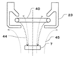
光電子スペクトル又は光電子イメージの測定を開始していない場合は、図4のように、帯電補償電子源電源41が帯電補償電子源40から発生した熱電子を0.1〜10eVに加速して試料7に熱電子44を供給し、広い範囲の試料7を中和する。
When the measurement of the photoelectron spectrum or photoelectron image has not been started, as shown in FIG. 4, the charge compensating electron
光電子スペクトル又は光電子イメージの測定している場合は、図5のように、帯電補償電子源電源41が加速を中止し、フィラメント40から発生した熱電子44の初期エネルギーで帯電した試料7表面の正電荷を中和する。つまり、試料7表面から光電子が放出されることによる正の帯電によって発生する静電場によって熱電子44が試料7表面上に選択的に供給され、不均一な帯電を除去される。
When the photoelectron spectrum or the photoelectron image is measured, as shown in FIG. 5, the charge compensating electron
なお、図2のように帯電補償電子源40は接地電極23内に配置されているため、試料7より発生した光電子は帯電補償電子源40まで到達せず、帯電補償電子源40から2次電子が発生することはない。
Since the charge
上記例では、主倍率制御レンズ34はオフされたが、この主倍率制御レンズ34を用いて、試料から発生した光電子を視野制限絞り27上に結像するようにしても良い。その場合、磁界型結像レンズ14はオフされ、主倍率制御レンズ34と補助倍率制御レンズ35によって、試料から発生した光電子は視野制限絞り27上に結像される。
In the above example, the main
このときには、光電子が視野制限絞り27上に常に結像するように、主倍率制御レンズ34の電圧V1と補助倍率制御レンズ35の電圧V2が変更されて、レンズ倍率が変更される。
At this time, the lens magnification is changed by changing the voltage V1 of the main
磁場型結像レンズ14を使用しない場合においても、帯電補償電子源電源41を用いて帯電補償のための電子を試料表面上に供給できる。
Even when the magnetic
以上、本発明の一例を、図1の電子分光装置を用いて説明した。 As described above, an example of the present invention has been described using the electron spectrometer of FIG.
なお、本発明は上記例に限定されるものではない。 The present invention is not limited to the above example.
例えば、上記例ではX線を試料に照射しているが、X線源の代わりに真空紫外光源(ヘリウム共鳴線源)を装置に組込み、真空紫外光を試料に照射するようにしても良い。このように、低いエネルギーの1次線を試料に当てることにより、試料表面の化学状態変化を、得られた価電子帯のスペクトルから求めることができる。 For example, in the above example, the sample is irradiated with X-rays, but instead of the X-ray source, a vacuum ultraviolet light source (helium resonance radiation source) may be incorporated in the apparatus so that the sample is irradiated with vacuum ultraviolet light. Thus, by applying a low energy primary line to the sample, the chemical state change of the sample surface can be obtained from the obtained spectrum of the valence band.
また、本発明は、電子ビームにより試料を励起し、それにより発生したオージェ電子のエネルギーを分析するオージェ電子分光装置等にも適用することができる。 The present invention can also be applied to an Auger electron spectrometer that excites a sample with an electron beam and analyzes the energy of Auger electrons generated thereby.
さらに、図1の装置において、視野制限絞り27の前段に偏向手段を設けるようにしてもよい。たとえば、接地電極24の内側に、視野制限絞り27の前段に形成される電場E(主倍率制御レンズ34と補助倍率制御レンズ35によって形成される電場)をX、Y方向に偏向させるための偏向手段を設けるようにしてもよい。
Further, in the apparatus shown in FIG. 1, a deflecting unit may be provided in front of the
そして、上述した試料分析のときに、視野制限絞り27の開口径を微小領域分析に対応した大きさに設定し、偏向手段により電場Eを二次元的に走査させるようにすれば、試料上の大領域Aについて、その大領域A中の各ポイント(各微小領域)から発生した光電子を順にアラナイザ21に取り込んで検出器22で検出することができる。この場合、制御装置5は、偏向手段による走査に対応させて検出器22からの信号を内部メモリに書き込み、その記憶した情報に基づき、試料表面領域についての化学状態マップを表示画面上に表示させる。
Then, in the above-described sample analysis, if the aperture diameter of the
1…分析室チャンバ、2…分析室、3…排気装置、4…真空ゲージ、5…制御装置、6…X線源、7…試料、8…X線源電源、9…試料ホルダ、10…試料ステージ、11…試料ステージ位置調整機構、12…電流供給部、13…加熱電源、14…磁界型結像レンズ、19…電子分光器、20…インプットレンズ、21…アナライザ、22…検出器、23、24、25、26…接地電極、27…視野制限絞り、28…開口径調整機構、29…角度制限絞り、30…開口径調整機構、31…入射スリット、32…電源ユニット、33…表示装置、34…主倍率制御レンズ(L1)、35…補助倍率制御レンズ(L2)、36…結像レンズ(L3)、37…減速レンズ(LR)、38…帯電補償電子銃、40…帯電補償電子源、41…帯電補償電子源電源、42…加熱電源、43…加速電源、44…熱電子、45…磁界線、100…ガス反応セル、101…分析室チャンバ、102…加熱ヒータ、103…試料、105…排気装置、106…X線源、107…電子分光器、108…インプットレンズ、109…絞り、110…アナライザ
DESCRIPTION OF SYMBOLS 1 ... Analysis chamber, 2 ... Analysis chamber, 3 ... Exhaust device, 4 ... Vacuum gauge, 5 ... Control device, 6 ... X-ray source, 7 ... Sample, 8 ... X-ray source power supply, 9 ... Sample holder, 10 ... Sample stage, 11 ... Sample stage position adjusting mechanism, 12 ... Current supply unit, 13 ... Heating power supply, 14 ... Magnetic imaging lens, 19 ... Electron spectrometer, 20 ... Input lens, 21 ... Analyzer, 22 ... Detector, 23, 24, 25, 26 ... ground electrode, 27 ... field limiting aperture, 28 ... aperture diameter adjusting mechanism, 29 ... angle limiting aperture, 30 ... aperture diameter adjusting mechanism, 31 ... entrance slit, 32 ... power supply unit, 33 ... display Device: 34: Main magnification control lens (L1), 35: Auxiliary magnification control lens (L2), 36: Imaging lens (L3), 37: Deceleration lens (LR), 38: Charge compensation electron gun, 40: Charge compensation Electron source, 41 ... charging compensation electricity
Claims (4)
前記試料を励起して2次荷電粒子を発生させる励起線源と、
前記2次荷電粒子を捕集する捕集レンズと、
前記捕集レンズで捕集した前記2次荷電粒子を検出するアナライザと、
前記2次荷電粒子が発生した前記試料を電子により中和する電子供給源と、
前記電子供給源から供給された前記電子を前記試料へ加速する電子加速手段と、を備えた荷電粒子エネルギー分析装置であって、
前記捕集レンズと前記試料との間に前記2次荷電粒子を前記捕集レンズに向けて通過させる開口を有する接地電極を設け、
前記電子供給源を前記接地電極内に配置するようにした荷電粒子エネルギー分析装置。 A magnetic lens that immerses the sample in a magnetic field;
An excitation source that excites the sample to generate secondary charged particles;
A collection lens for collecting the secondary charged particles;
An analyzer for detecting the secondary charged particles collected by the collection lens;
An electron supply source for neutralizing the sample in which the secondary charged particles are generated with electrons;
An electron acceleration means for accelerating the electrons supplied from the electron supply source to the sample, and a charged particle energy analyzer comprising:
A ground electrode having an opening through which the secondary charged particles pass toward the collecting lens is provided between the collecting lens and the sample,
A charged particle energy analyzer configured to arrange the electron supply source in the ground electrode.
前記2次荷電粒子を測定していないときは前記電子加速制御手段が前記電子を加速するよう制御して前記試料を中和し、
前記2次荷電粒子の測定中は前記電子加速制御手段が前記電子を加速しないように制御して前記試料を中和する荷電粒子エネルギー分析装置。 The charged particle energy analyzer according to claim 1 or 2, further comprising an electron acceleration control means for controlling the electron acceleration means,
When the secondary charged particle is not measured, the electron acceleration control means controls the electron to accelerate and neutralizes the sample,
A charged particle energy analyzer that neutralizes the sample by controlling the electron acceleration control means not to accelerate the electrons during measurement of the secondary charged particles.
The charged particle energy analyzer according to claim 1, wherein the secondary charged particles are photoelectrons.
Priority Applications (1)
| Application Number | Priority Date | Filing Date | Title |
|---|---|---|---|
| JP2004109567A JP2005292013A (en) | 2004-04-02 | 2004-04-02 | Surface analyzer |
Applications Claiming Priority (1)
| Application Number | Priority Date | Filing Date | Title |
|---|---|---|---|
| JP2004109567A JP2005292013A (en) | 2004-04-02 | 2004-04-02 | Surface analyzer |
Publications (1)
| Publication Number | Publication Date |
|---|---|
| JP2005292013A true JP2005292013A (en) | 2005-10-20 |
Family
ID=35325093
Family Applications (1)
| Application Number | Title | Priority Date | Filing Date |
|---|---|---|---|
| JP2004109567A Pending JP2005292013A (en) | 2004-04-02 | 2004-04-02 | Surface analyzer |
Country Status (1)
| Country | Link |
|---|---|
| JP (1) | JP2005292013A (en) |
Cited By (3)
| Publication number | Priority date | Publication date | Assignee | Title |
|---|---|---|---|---|
| JP2006349384A (en) * | 2005-06-13 | 2006-12-28 | National Institute For Materials Science | Radiation electron microscope apparatus and sample observation method for suppressing charging or potential distortion of insulating sample |
| JP2007165155A (en) * | 2005-12-14 | 2007-06-28 | National Institute For Materials Science | Radiation electron microscope for observation of insulator samples using obliquely charged neutralized electron irradiation method |
| WO2026018299A1 (en) * | 2024-07-16 | 2026-01-22 | 株式会社日立ハイテク | Photoelectron microscope and defect detection method |
Citations (3)
| Publication number | Priority date | Publication date | Assignee | Title |
|---|---|---|---|---|
| JPH04249754A (en) * | 1990-10-16 | 1992-09-04 | Seiko Instr Inc | Method and apparatus for photoelectronic spectroscopy for chemical analysis |
| JP2003187738A (en) * | 2001-12-20 | 2003-07-04 | Jeol Ltd | Electron spectrometer, electron spectrometer, and sample analysis method |
| JP2004085546A (en) * | 2002-06-28 | 2004-03-18 | Canon Inc | Element information acquisition method by time-of-flight secondary ion mass spectrometry and information acquisition apparatus |
-
2004
- 2004-04-02 JP JP2004109567A patent/JP2005292013A/en active Pending
Patent Citations (3)
| Publication number | Priority date | Publication date | Assignee | Title |
|---|---|---|---|---|
| JPH04249754A (en) * | 1990-10-16 | 1992-09-04 | Seiko Instr Inc | Method and apparatus for photoelectronic spectroscopy for chemical analysis |
| JP2003187738A (en) * | 2001-12-20 | 2003-07-04 | Jeol Ltd | Electron spectrometer, electron spectrometer, and sample analysis method |
| JP2004085546A (en) * | 2002-06-28 | 2004-03-18 | Canon Inc | Element information acquisition method by time-of-flight secondary ion mass spectrometry and information acquisition apparatus |
Cited By (3)
| Publication number | Priority date | Publication date | Assignee | Title |
|---|---|---|---|---|
| JP2006349384A (en) * | 2005-06-13 | 2006-12-28 | National Institute For Materials Science | Radiation electron microscope apparatus and sample observation method for suppressing charging or potential distortion of insulating sample |
| JP2007165155A (en) * | 2005-12-14 | 2007-06-28 | National Institute For Materials Science | Radiation electron microscope for observation of insulator samples using obliquely charged neutralized electron irradiation method |
| WO2026018299A1 (en) * | 2024-07-16 | 2026-01-22 | 株式会社日立ハイテク | Photoelectron microscope and defect detection method |
Similar Documents
| Publication | Publication Date | Title |
|---|---|---|
| JP4302316B2 (en) | Scanning electron microscope | |
| US7960697B2 (en) | Electron beam apparatus | |
| JP4236742B2 (en) | Scanning electron microscope | |
| US8378299B2 (en) | Twin beam charged particle column and method of operating thereof | |
| US6043491A (en) | Scanning electron microscope | |
| TWI662580B (en) | Charged particle beam specimen inspection system and method for operation thereof | |
| CN112970088A (en) | Particle beam system for adjusting the current of individual particle beams | |
| JPWO1999046798A1 (en) | scanning electron microscope | |
| JP3616714B2 (en) | Apparatus for setting a predetermined surface potential on an insulating sample in an analytical instrument | |
| JPH0727556Y2 (en) | Charged particle energy analyzer | |
| US20180151329A1 (en) | Time-of-flight charged particle spectroscopy | |
| JPWO2019064496A1 (en) | Scanning electron microscope | |
| US6815678B2 (en) | Raster electron microscope | |
| KR100695983B1 (en) | Scanning electron microscope | |
| JP4590590B2 (en) | SEM for transmission operation with position sensitive detector | |
| US5451783A (en) | Charged-particle analyser | |
| JP2005292013A (en) | Surface analyzer | |
| US9543115B2 (en) | Electron microscope | |
| JPH0955181A (en) | Scanning electron microscope | |
| JP3683156B2 (en) | Method for surface analysis of solid materials | |
| JP3730041B2 (en) | Method for accelerating emitted electrons in a composite emission electron microscope | |
| JP2000304712A (en) | Electron beam analyzer / observer and electron beam micro analyzer | |
| JP2003187738A (en) | Electron spectrometer, electron spectrometer, and sample analysis method | |
| JP3965691B2 (en) | Scanning electron microscope | |
| JP2002352759A (en) | Electron beam device with field emission electron gun |
Legal Events
| Date | Code | Title | Description |
|---|---|---|---|
| A621 | Written request for application examination |
Free format text: JAPANESE INTERMEDIATE CODE: A621 Effective date: 20061130 |
|
| A977 | Report on retrieval |
Free format text: JAPANESE INTERMEDIATE CODE: A971007 Effective date: 20090311 |
|
| A131 | Notification of reasons for refusal |
Free format text: JAPANESE INTERMEDIATE CODE: A131 Effective date: 20091117 |
|
| A02 | Decision of refusal |
Free format text: JAPANESE INTERMEDIATE CODE: A02 Effective date: 20100413 |