JP4236742B2 - Scanning electron microscope - Google Patents
Scanning electron microscope Download PDFInfo
- Publication number
- JP4236742B2 JP4236742B2 JP30805598A JP30805598A JP4236742B2 JP 4236742 B2 JP4236742 B2 JP 4236742B2 JP 30805598 A JP30805598 A JP 30805598A JP 30805598 A JP30805598 A JP 30805598A JP 4236742 B2 JP4236742 B2 JP 4236742B2
- Authority
- JP
- Japan
- Prior art keywords
- sample
- electrode
- voltage
- electron beam
- objective lens
- Prior art date
- Legal status (The legal status is an assumption and is not a legal conclusion. Google has not performed a legal analysis and makes no representation as to the accuracy of the status listed.)
- Expired - Lifetime
Links
- 238000010894 electron beam technology Methods 0.000 claims description 53
- 230000005684 electric field Effects 0.000 claims description 39
- 230000001133 acceleration Effects 0.000 claims description 30
- 230000003287 optical effect Effects 0.000 claims description 3
- 230000008859 change Effects 0.000 claims description 2
- 230000000979 retarding effect Effects 0.000 description 34
- 238000000034 method Methods 0.000 description 16
- 230000001681 protective effect Effects 0.000 description 15
- 239000004065 semiconductor Substances 0.000 description 8
- 238000010586 diagram Methods 0.000 description 7
- 238000000605 extraction Methods 0.000 description 5
- 239000012212 insulator Substances 0.000 description 5
- 230000006378 damage Effects 0.000 description 3
- 238000001514 detection method Methods 0.000 description 3
- 230000000694 effects Effects 0.000 description 3
- 230000006870 function Effects 0.000 description 3
- 238000007689 inspection Methods 0.000 description 3
- XUIMIQQOPSSXEZ-UHFFFAOYSA-N Silicon Chemical compound [Si] XUIMIQQOPSSXEZ-UHFFFAOYSA-N 0.000 description 2
- 230000009471 action Effects 0.000 description 2
- 230000004075 alteration Effects 0.000 description 2
- 230000007246 mechanism Effects 0.000 description 2
- 230000008569 process Effects 0.000 description 2
- 229910052710 silicon Inorganic materials 0.000 description 2
- 239000010703 silicon Substances 0.000 description 2
- 238000013016 damping Methods 0.000 description 1
- 230000006866 deterioration Effects 0.000 description 1
- 238000009826 distribution Methods 0.000 description 1
- PCHJSUWPFVWCPO-UHFFFAOYSA-N gold Chemical compound [Au] PCHJSUWPFVWCPO-UHFFFAOYSA-N 0.000 description 1
- 239000010931 gold Substances 0.000 description 1
- 229910052737 gold Inorganic materials 0.000 description 1
- 238000010438 heat treatment Methods 0.000 description 1
- 230000006872 improvement Effects 0.000 description 1
- 239000000463 material Substances 0.000 description 1
- 238000005259 measurement Methods 0.000 description 1
- 238000005389 semiconductor device fabrication Methods 0.000 description 1
- 238000004904 shortening Methods 0.000 description 1
- 238000007740 vapor deposition Methods 0.000 description 1
Images


Classifications
-
- H—ELECTRICITY
- H01—ELECTRIC ELEMENTS
- H01J—ELECTRIC DISCHARGE TUBES OR DISCHARGE LAMPS
- H01J37/00—Discharge tubes with provision for introducing objects or material to be exposed to the discharge, e.g. for the purpose of examination or processing thereof
- H01J37/26—Electron or ion microscopes; Electron or ion diffraction tubes
- H01J37/28—Electron or ion microscopes; Electron or ion diffraction tubes with scanning beams
-
- H—ELECTRICITY
- H01—ELECTRIC ELEMENTS
- H01J—ELECTRIC DISCHARGE TUBES OR DISCHARGE LAMPS
- H01J2237/00—Discharge tubes exposing object to beam, e.g. for analysis treatment, etching, imaging
- H01J2237/04—Means for controlling the discharge
- H01J2237/047—Changing particle velocity
Landscapes
- Chemical & Material Sciences (AREA)
- Analytical Chemistry (AREA)
- Analysing Materials By The Use Of Radiation (AREA)
Description
【0001】
【発明の属する技術分野】
本発明は、試料表面に電子ビームを走査し、試料から発生する二次信号を検出することで試料表面の形状あるいは組成等を表わす二次元の走査像を得る走査形電子顕微鏡に関し、特に低加速電圧の領域で半導体試料を分解能で観察するのに好適な走査形電子顕微鏡に関する。
【0002】
【従来の技術】
走査形電子顕微鏡は、加熱形または電界放出形の電子源から放出された電子を加速し、静電または磁界レンズを用いて細い電子ビーム(一次電子線)とし、該一次電子線を観察する試料上に二次元走査し、該一次電子線照射で試料から二次的に発生する二次電子または反射電子等の二次信号を検出し、検出信号強度を一次電子ビームの走査と同期して走査されるブラウン管の輝度変調入力とすることで二次元の走査像を得る装置である。
【0003】
走査形電子顕微鏡では、負電圧を印加した電子源から放出された電子を接地電圧の陽極で加速し、接地電圧にある検査試料に一次電子ビームを走査する。半導体産業の微細化が進んだことから、走査形電子顕微鏡が光学顕微鏡に代わって、半導体素子製作のプロセスまたはプロセス完成後の検査(例えば電子ビームによる寸法測定や電機的動作の検査)に使われるようになった。絶縁物が使われている半導体産業の試料(ウェハ)では、絶縁物を帯電することなく観察できる1kV以下の低加速電圧が必要である。前述した一般のSEMでは、1kVの分解能は約10nmであった。半導体の微細化に伴い、10nm以下のより高分解能が得られる低加速電圧の走査電子顕微鏡を要求されるようになった。
【0004】
その解決方法の一つとして、リターディング法が知られている。1kV以上の高い加速電圧の一次電子ビームを細く絞り、試料に照射する際に、試料に負電圧を印加しておく。
【0005】
すなわち、照射した一次電子ビームを試料に印加した負電圧で、試料に入射する直前に所望の加速電圧に低下させる。このリターディング法を用いると、対物レンズのレンズ収差が低減し、分解能の向上を得ることが出来る。この基本的な構成はUltramicroscopy 41(1992)の402ページ、図3に示されている。
【0006】
【発明が解決しようとする課題】
特開平9−171791 号公報には、リターディング方式を採用した走査形電子顕微鏡が開示されている。当該公報によれば、試料に負電圧を印加するリターディング法に加え、対物レンズ内で一次電子線をさらに加速する後段加速法(ブースティング法)も採用されている。このブースティング法もリターディング法と同様に分解能の向上に寄与するものである。
【0007】
当該公報には、試料ホルダと対物レンズの間に配置され、試料ホルダと同じ負の電圧が印加される電極が開示されている。このように構成によれば、試料の上下に負の電圧が印加される導電部材が配置されることになる。この構成では試料が絶縁物であっても、試料に所望の負電圧(以下リターディング電圧とする)を印加することが可能になる。
【0008】
例えば試料が、表裏面及び裏面が酸化膜で覆われたシリコンウェハの場合、単に試料ホルダに負電圧を印加するだけでは、試料に印加される電圧は、試料と対物レンズ間の静電容量で配分される電圧となり、本来予定していた正しいリターディング電圧を印加することができなくなる。
【0009】
それに対し、特開平9−171791 号公報に開示の技術は、このような問題を解決するためのものである。
【0010】
即ち試料が絶縁物であっても、同じ負電圧が印加される導電部材間に形成される前記負電圧と同電位の空間領域に、試料を配置することで、所望のリターディング電圧の印加を可能としている。
【0011】
このような目的のもと、配置される電極(以下保護電極とする)には、一次電子線を通過させるための開口が設けられている。この開口は、一次電子線の照射点と外部素子(対物レンズやブースティング電極)との電位差によって生ずる電界が、照射点に及ぶように大きさが決められている。この開口が狭く、照射点に電界が及ばないようになると、一次電子線の照射点で発生する二次信号(特に二次電子)が、検出器側に導かれなくなるという問題があるからである。
【0012】
一方、特開平9−171791 号公報で開示されているブースティング法では、強い正の電圧が印加される加速筒が、対物レンズの電子線通過口内に配置される。この構成によれば、試料と加速筒との間に強い電界が形成されることになるため、半導体試料の種類によっては、素子が破壊、或いは劣化する場合がある。
【0013】
以上のように試料と外部素子との間に或る程度の電界を生じさせたいという要求がある反面、加速筒と試料間に形成されるような強電界を試料上に形成したくないという要求がある。
【0014】
本発明はこのような要求に答えるものであり、リターディング法と後段加速法を併用した走査形電子顕微鏡において、試料に強い電界を与えることなく、二次信号を検出器側に導くのに必要にして十分な電界を形成するのに好適な構成からなる走査形電子顕微鏡を提供することを目的とするものである。
【0015】
【課題を解決するための手段】
本発明は上記目的を達成するために、電子源と、該電子源から放出される一次電子線を収束するための対物レンズと、該対物レンズによって収束された一次電子線の照射により試料から発生する電子を検出する検出器を備えた走査形電子顕微鏡において、前記試料を配置する試料ホルダと、前記試料と前記対物レンズの間に配置され、前記一次電子線の通過開口を備えた保護電極と、前記試料ホルダと前記保護電極に負の電圧を印加するための負電圧印加手段と、前記対物レンズの電子線通過口内に配置され、通過する電子を加速する加速筒と、前記保護電極の前記通過開口より小さな通過開口を有し、前記負の電圧に対して正の電圧が与えられる制御電極を、前記加速筒と前記試料との間に配置したことを特徴とする走査形電子顕微鏡を提供する。
【0016】
このような構成によれば、加速筒と試料との間に形成される強い電界を、その間に配置される制御電極の存在によって抑制することができ、しかも試料に印加される負の電圧に対して正の電圧が与えられているので一次電子線の照射点で発生した二次信号を制御電極の開口上まで導くことができる。
【0017】
【発明の実施の形態】
本発明の理解を助けるために、本発明の制御電極がない走査形電子顕微鏡と、本発明の制御電極を採用した走査形電子顕微鏡を対比して説明する。
【0018】
図1は、制御電極がない走査形電子顕微鏡の構成を示す図である。電界放出陰極1と引出電極2との間に引出電圧3を印加すると、放出電子4が放出される。放出電子4は、引出電極2と接地電圧にある陽極5の間でさらに加速(減速の場合もある)される。陽極5を通過した電子ビーム(一次電子線7)の加速電圧は電子銃加速電圧6と一致する。
【0019】
陽極5で加速された一次電子線7はコンデンサレンズ14で収束され、上走査偏向器15,下走査偏向器16で走査偏向を受ける。上走査偏向器15,下走査偏向器16の偏向強度は、対物レンズ17のレンズ中心を支点として試料12上を二次元走査するように調整されている。
【0020】
偏向を受けた一次電子線7は、対物レンズ17の通路に設けられた加速円筒9(加速筒)で、さらに後段加速電圧電源22で印加される電圧分の加速をうける。後段加速された一次電子線7は、対物レンズ17のレンズ作用で試料12上に細く絞られる。対物レンズ17を通過した一次電子線7は、試料12に印加した負のリターディング電圧電源13で印加される電圧によって対物レンズ17と試料12間に作られる減速電界で減速されて試料12に到達する。
【0021】
この構成によれば、対物レンズ17を通過するときの一次電子線7の加速電圧は、電子銃加速電圧6+後段加速電圧電源22で印加される電圧で、試料12に入射する加速電圧(電子銃加速電圧6−リターディング電圧電源13で印加される電圧)より高くなっている。この結果、試料に入射する加速電圧の一次電子線(電子銃加速電圧6−リターディング電圧電源13で印加される電圧)を対物レンズ17で絞る場合に比較し、より細かい電子ビーム(高い分解能)が得られる。これは対物レンズ17の色収差が減少することによる。
【0022】
典型的な例では、電子銃加速電圧6で印加される電圧を2kV,後段加速電圧電源22で印加される電圧を7kV,リターディング電圧電源13で印加される電圧を1kVとする。
【0023】
この例では、一次電子線7は対物レンズ17内を9kVで通過し、試料に入射する加速電圧は1kVになる。この例での分解能は、1kVの一次電子線を絞ったときの分解能10nmに比較すると、約3分の1の3nmに改善される。
【0024】
一次電子ビーム7が試料12を照射すると二次信号23が発生する。ここで考慮する二次信号23は二次電子と反射電子である。対物レンズ17と試料12との間に形成される電界、或いは試料12と加速円筒9との間に形成される電界は、発生した二次信号23に対しては加速電界として作用するため、対物レンズ17の通過内に吸引され、対物レンズ17の磁界ではレンズ作用を受けながら上昇する。
【0025】
対物レンズ17内を通過した二次信号23は走査偏向器15,16を通過し、反射板29に衝突する。この反射板29は中央に一次電子ビーム7を通過させる開口を持った導電性の板である。二次信号23が衝突する面は二次電子の発生効率のよい物質、例えば金蒸着面になっている。二次信号23(二次電子と反射電子)は、ほぼ同じ軌道を通って反射板29に衝突する。
【0026】
反射板29に衝突した二次電子と反射電子は、ここで二次電子30を発生させる。反射板29で作られた二次電子30は接地に対して負電圧を印加した静電偏向電極31aと正電圧を印加した静電偏向電極31bで偏向される。静電偏向電極31bはメッシュ状で、偏向された二次電子30が通過できるようになっている。33a,33bは磁界偏向コイルで、静電偏向電極31a,31bの作る電界と直交する磁界を発生させ、静電偏向による一次電子ビーム7の偏向を打消すようになっている。
【0027】
メッシュ状の静電偏向電極31bを通過した二次電子は正の10kV高電圧が印加されたシンチレータ32に吸引され、シンチレータ32に衝突し、光を発生する。この光をライトガイド24で光電子倍増管18に導き、電気信号に変換し、増幅する。この出力でブラウン管の輝度変調を行う(図示せず)。
【0028】
絞り8は一次電子ビーム7の開口角を制御するもので調整つまみ10によって軸合せができるようになっている。19は試料12をXYに移動するためのXY移動機構で、この上に絶縁板21で絶縁された試料ホルダ20が置かれ、これにリターディング電圧電源13が印加されている。このホルダ20に試料(例えばウェハ)を載せる。載せることで試料12にもリターディング電圧電源13が印加される。
【0029】
この試料12を覆うように保護電極27が設置されている。この保護電極27は試料が絶縁物であっても、試料に所望のリターディング電圧電源13を印加するための物である。典型的な例は半導体の試料で、裏面および側面が酸化膜で覆われたシリコンウェハである。
【0030】
このような試料を試料ホルダ20に載せ、リターディング電圧電源13を印加しても試料(ウェハ)12の電圧は、試料ホルダ20と試料12間の静電容量と、試料12と対物レンズ17間の静電容量で配分される電圧になる。試料12には、正しくリターディング電圧電源13が印加されないことになる。
【0031】
保護電極27はこれを防止するためのもので、試料12全体を覆い、ホルダ20と同じ電圧が印加されている。保護電極27には、電子ビーム11を通す開口が設けられている。この開口の典型的な大きさは直径20mmで、試料12と対物レンズ17の下面間の距離は3mmである。この大きさは、観察する試料領域の減速電界が保護電極27としての効果への影響は非常に小さい。
【0032】
典型的な例として、電子銃加速電圧6を2kV,後段加速電圧電源22を7kV,リターディング電圧電源13を1kVとした例を示す。この例では、対物レンズ17と試料12間の電界強度は3kV/cmにある。また、さらに高分解能を得ようとする場合には、電子銃加速電圧6と後段加速電圧電源22を高くする必要がある。この結果、さらに強い電界が試料12の表面に印加されることになる。半導体の素子によっては、この電界によって破壊あるいは劣化を受ける可能性がある。
【0033】
また、この減速電界は二次信号を対物レンズ17の上方に導くために必要なもので、ある程度の強さは必要である。すなわち、保護電極27は、1)絶縁された試料12をリターディング電圧電源13に保つ機能効果をもち、2)二次信号を対物レンズ17の上方に引き上げるに必要で、かつ試料12を破損を与えない電界強度を与える機能を持つことが必要である。しかるに、図1の装置では、上述の機能を満足できない。
【0034】
図2は、本発明の制御電極を採用した走査形電子顕微鏡の実施例を示す図である。本実施例では、保護電極27と対物レンズ17との間に制御電極28が付加され、これに制御電圧電源36が印加されている。制御電圧電源36にリターディング電圧電源13と同じ電圧を印加すると制御電極28は接地電圧になり、制御電極28の無い状態とほぼ同じ電界が試料12の表面に印加される。制御電圧電源36を零にすると試料12の表面の電界も零になる。すなわち、制御電圧電源36を調整することにより試料表面の電界を任意に制御することが可能である。
【0035】
この制御電圧電源36を固定しておくと、リターディング電圧電源13に関係なく、一定の電界を試料12の表面に印加することができる。保護電極27の開口は直径20mmで制御電極28の電界が試料12の表面に侵入できるようになっている。
【0036】
なお、この制御電圧電源36を可変電源とし、操作者が任意の電圧に調整できるようにしておくことが望ましい。例えば試料の種類によっては、表面に形成される電界に対して強いものと、そうでないものがある。一方、試料の破損等を問題にしないのであれば、試料と外部素子(本発明実施例装置の場合、制御電極28)との電位差が大きい方がより二次信号を制御電極28上に導くことができる。この兼ね合いにより制御電極28に印加する電圧を決定すれば良い。
【0037】
また、図示しない入力装置で観察対象となる試料の種類(組成)を入力することによって、制御電極28に与えられる電圧が自動的に決定されるようにしても良い。この場合、図示しないメモリに予め試料の種類と制御電極に印加する電圧の関係を記憶させ、入力に応じて自動的に電圧が選択されるような装置構成が必要となる。
【0038】
本発明では、コンデンサレンズ14と上走査偏向器15の間に検出器が2段 (第1と第2)設けられている。第1検出器34は図1と同一構造である。第2検出器35もほぼ同様の構成であるが、静電偏向電極41a,41bの偏向電圧(偏向負電圧46と偏向正電圧47)の中点に、試料12に印加されているリターディング電圧電源13が供給されている。
【0039】
また、反射板は設置されていない。この実施例における二次信号23検出について説明する。電子銃加速電圧6を2kV,後段加速電圧電源22を7kV,リターディング電圧電源13を1kVとする。試料12で発生した二次信号23 (放出エネルギーは0から約10Vに分布し、約2Vにピークをもつ二次電子と放出エネルギーが1kVの反射電子)は、試料12に印加されたリターディング電圧電源13と後段加速電圧電源22で加速され、二次電子は8kVで、反射電子は9kVで対物レンズ17を通過する。後段加速円筒9を通過時に後段加速電圧電源22の減速を受け、二次電子は1kVに、反射電子は2kVになる。
【0040】
下検出器の静電偏向電極41a,41bの中点にリターディング電圧電源13が印加されているため、静電偏向電極41aと41bで作られる領域に入る時点でさらに減速を受け、二次電子,反射電子とも放出時のエネルギーになる(二次電子:0〜約10V,反射電子:約1kV)。
【0041】
エネルギーの低い二次電子50のみが静電偏向電極41a,41bの作る電界で偏向され、メッシュ状の静電偏向電極41bを通過して、シンチレータ43を光らせ、ライトガイド44,光電子増倍管45に導かれて電気信号に変換,増幅される。ここで検出されるのは二次電子のみである。
【0042】
磁界偏向コイル40a,40bは静電偏向電極41a,41bによる一次電子ビーム7の偏向を補正する。
【0043】
一方、反射電子51は約1kVのエネルギーを持っている。このため静電偏向電極41a,41bの作る電界でほとんど偏向されることなく下検出器を通過する。通過時に反射電子51はリターディング電圧電源13による加速を受けて、約2kVで第2検出器35に入り、反射板29に衝突する。
【0044】
ここで発生した二次電子30は静電偏向電極31a,31bで偏向され、メッシュ状の静電偏向電極31bを通過して、検出される。ここで検出される信号は反射電子51の強度を反映したものになる。このように本実施例では、二次電子と反射電子を完全に分離して検出することが可能になる。
【0045】
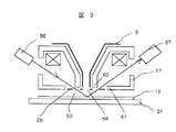
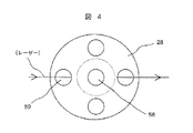
図3にレーザーによる試料12の高さ検出器(Zセンサー)を備えた場合の制御電極28の構造を示す。図には変更のある対物レンズ部分のみを示した。制御電極28は対物レンズ17の下磁極61に保持されている。制御電極28には、電子ビームを通す電子ビーム開口58とZセンサーのレーザーが通るレーザー開口59が設けられている。図4に制御電極28の平面図を示した。中央に電子ビーム開口58があり、周囲に4箇所のレーザー開口59が設けられている。レーザーは対称なレーザー開口の片側から入り、もう一方から出ていく。レーザー開口を4箇所とすることで電子ビーム開口58部分の電界分布が非対称にならないように考慮されている。
【0046】
ここでは制御電極28を対物レンズ17の下磁極に保持した例を示したが、上磁極60に保持してもよい。この場合は図4の点線で示すような円盤になり、レーザー開口59は不要になる。
【0047】
図5に第1検出器34の詳細を説明する。図に光軸に直交する断面構造を示した。静電偏向電極41a,41bは円筒を縦割りにした構造をしている。静電偏向電極41bはメッシュで偏向した二次電子50が通過できるようになっている。二次電子50を偏向する電界Eは偏向負電圧46と偏向正電圧で作る。通常、この偏向負電圧46,偏向正電圧47は同じ値である。
【0048】
偏向負電圧46と偏向正電圧47の中点にリターディング電圧が印加されている。偏向コイル40a,40bは電界Eと直交する偏向磁場Bを作る。この磁場は、一次電子の偏向電界Eによる偏向を打消すように強度と方向が調整される。この磁場は二次電子50に対しては偏向を強めるように働く。静電偏向電極41bの外周にフィルターメッシュ42が設置されている。これは二次電子50を放出エネルギーの差で分離するためのもので、偏向負電圧46,偏向正電圧47の中点に対してフィルター電圧電源48を与えることでエネルギーの分別を行う。
【0049】
正電圧を与えると、総てのエネルギー範囲の二次電子を通過させ、負電圧を与えることで負電圧に相当するエネルギー以下の二次電子を追い返すため、フィルターメッシュ42を通過する二次電子は高いエネルギーを持ったもののみになる。フィルターメッシュ42を通過した二次電子は、10kVgが印加されたシンチレータ43に吸引,加速され、シンチレータ43を光らせる。発光した光はライトガイド44に導かれる。
【0050】
尚、図2において静電偏向電極41a,41bの中点に印加しているリターディング電圧電源13をOFFとし、二次電子も上方に導き、上段の検出器で二次電子,反射電子の両方を検出するようにすることも可能である。
【0051】
図2の実施例では、第1検出器34の静電偏向電極41aと41bの中点にリターディング電圧を印加したが、これに電圧を重畳することでも二次電子のうちの特定なエネルギーを選択して検出ことが可能になる。
【0052】
図6に実施例を示した。この実施例では、エネルギーの低い二次電子を選択的に検出している。静電偏向電極41aと41bの上下に上メッシュ54と下メッシュ55が設置され、静電偏向電極41aと41bの偏向負電圧46,偏向正電圧47の中点に接続されている。
【0053】
この例では重畳電圧53に正電圧を印加する。例えば、5Vの電圧とする。こうすると静電偏向電極41aと41bの領域内での二次電子のエネルギーは5V高くなる。放出エネルギーの高い二次電子はよりエネルギーが高くなるため偏向量が少なくなり、図に示すように検出されることなく通過してしまう。この例のように制電圧を重畳することで放出エネルギーの低い二次電子のみを選択的に検出することができる。
【0054】
この実施例では、上下にメッシュ54,55を設置したが、これを省略しても同様な性能を得ることができる。また、この上下メッシュの中央には一次電子ビームを通過させる開口が設けられている。
【0055】
図7はエネルギーの高い二次電子を選択的に検出している様子を示した実施例である。負の重畳電圧53を与える。この結果、エネルギーの低い二次電子は下メッシュ55で追い返されてしまうため、検出される二次電子は下メッシュ55を通過できるエネルギーを持った高エネルギーの二次電子のみになる。
【0056】
図8は本発明の他の実施例である。この実施例では、対物レンズ17の磁路が上磁路
25,中磁路37,下面磁路38の三つに分割されている。下面磁路38は保護電極27を兼ねており、リターディング電圧電源13が印加されている。上磁路25には、後段加速電圧電源22が印加され、上磁路25が後段加速電極を兼ねている。この構造の特徴は、図1で必要とした保護電極27を挿入するスペースが不要になり、対物レンズ17の焦点距離を短く、すなわちより高分解能を得ることが可能になることである。
【0057】
特徴の第2は、図2で起こる可能性のある対物レンズの軸と後段加速電極との軸ずれがないことである。また、この実施例では、上磁路25の先端に制御電極28が設置され、これに制御電圧電源36が印加されている。
【0058】
この実施例の反射板29はシンチレータ32に向かって傾斜され、反射電子の衝突による二次電子発生効率の向上を計っている。
【0059】
尚、本発明では、試料にリターディング電圧電源13が印加されているが、このリターディング電圧電源13が印加されない場合でも同様であることは言うまでもない。
【0060】
【発明の効果】
本発明によれば、試料ホルダとの導通の取れない絶縁試料であっても所望のリターディング電圧を試料に供給することが可能な走査形電子顕微鏡において、試料の表面に過剰な電界を印加することなく、二次信号を検出器に導くに必要かつ十分な電界を形成することができるようになるので、二次信号の検出効率を低下させることなく、試料の破壊や劣化を防止することが可能になる。
【図面の簡単な説明】
【図1】従来の低加速電圧の走査顕微鏡の構造を説明する図。
【図2】本発明の構成を説明する図。
【図3】Zセンサーを装備した本発明の実施例を説明する図。
【図4】制御電極の構造例を説明する図。
【図5】二次電子の検出方法を説明する図。
【図6】低エネルギーの二次電子を選択的に検出する方法を説明する図。
【図7】高エネルギーの二次電子を選択的に検出する方法を説明する図。
【図8】本発明の他の実施例である。
【符号の説明】
1…電界放出陰極、2…引出電極、3…引出電圧、4…放出電子、5…陽極、6…電子銃加速電圧、7…一次電子ビーム、8…絞り、9…後段加速円筒、10…調整つまみ、12…試料、13…リターディング電圧電源、14…コンデンサレンズ、15…上走査偏向器、16…下走査偏向器、17…対物レンズ、18…光電子増倍管、19…XY移動機構、20…ホルダ、21…絶縁板、22…後段加速電圧電源、23…二次信号、24…ライドガイド、25…上磁路、26…下磁路、27…保護電極、28…制御電極、29…反射板、30,50…二次電子、31…静電偏向電極、32,43…シンチレータ、33…磁界偏向コイル、34…第1検出器、35…第2検出器、36…制御電圧電源、37…中磁路、38…下面磁路、40…磁界偏向コイル、41…静電偏向電極、42…フィルターメッシュ、44…ライトガイド、45…光電子増倍管、46…偏向負電圧電源、47…偏向正電圧電源、48…フィルター電圧電源、51…反射電子、53…重畳電圧、54…上メッシュ、55…下メッシュ、56…半導体レーザー、57…ポジションセンサー、58…電子ビーム開口、59…レーザー開口。[0001]
BACKGROUND OF THE INVENTION
The present invention relates to a scanning electron microscope that obtains a two-dimensional scanning image representing the shape or composition of a sample surface by scanning a sample surface with an electron beam and detecting a secondary signal generated from the sample. The present invention relates to a scanning electron microscope suitable for observing a semiconductor sample with resolution in a voltage region.
[0002]
[Prior art]
A scanning electron microscope accelerates electrons emitted from a heating type or field emission type electron source to form a thin electron beam (primary electron beam) using an electrostatic or magnetic lens, and observes the primary electron beam Two-dimensional scanning is performed, and secondary signals such as secondary electrons or backscattered electrons generated secondaryly from the sample by the irradiation of the primary electron beam are detected, and the detected signal intensity is scanned in synchronization with the scanning of the primary electron beam. This is a device that obtains a two-dimensional scanned image by using the luminance modulation input of a cathode ray tube.
[0003]
In the scanning electron microscope, electrons emitted from an electron source to which a negative voltage is applied are accelerated by an anode having a ground voltage, and a primary electron beam is scanned onto an inspection sample at the ground voltage. Due to the progress of miniaturization in the semiconductor industry, scanning electron microscopes are used in place of optical microscopes in the process of semiconductor device fabrication or inspection after completion of the process (for example, dimensional measurement using an electron beam or electrical operation inspection). It became so. A sample (wafer) in the semiconductor industry in which an insulator is used requires a low acceleration voltage of 1 kV or less that can be observed without charging the insulator. In the general SEM described above, the resolution of 1 kV was about 10 nm. With the miniaturization of semiconductors, a scanning electron microscope with a low acceleration voltage capable of obtaining a higher resolution of 10 nm or less has been required.
[0004]
As one of the solutions, the retarding method is known. When a primary electron beam with a high acceleration voltage of 1 kV or higher is narrowed down and irradiated on the sample, a negative voltage is applied to the sample.
[0005]
That is, the irradiated primary electron beam is reduced to a desired acceleration voltage immediately before entering the sample with a negative voltage applied to the sample. When this retarding method is used, the lens aberration of the objective lens is reduced, and the resolution can be improved. This basic configuration is shown in FIG. 3 on page 402 of Ultramicroscopy 41 (1992).
[0006]
[Problems to be solved by the invention]
Japanese Laid-Open Patent Publication No. 9-1771791 discloses a scanning electron microscope that employs a retarding method. According to the publication, in addition to the retarding method in which a negative voltage is applied to the sample, a post-acceleration method (boosting method) in which the primary electron beam is further accelerated in the objective lens is employed. This boosting method also contributes to the improvement of the resolution like the retarding method.
[0007]
The gazette discloses an electrode that is disposed between the sample holder and the objective lens and is applied with the same negative voltage as the sample holder. According to this configuration, conductive members to which a negative voltage is applied are arranged above and below the sample. In this configuration, even if the sample is an insulator, a desired negative voltage (hereinafter referred to as a retarding voltage) can be applied to the sample.
[0008]
For example, if the sample is a silicon wafer whose front and back surfaces and back surface are covered with an oxide film, simply applying a negative voltage to the sample holder will cause the voltage applied to the sample to be the capacitance between the sample and the objective lens. Thus, the correct retarding voltage originally intended cannot be applied.
[0009]
On the other hand, the technique disclosed in Japanese Patent Application Laid-Open No. 9-177171 is for solving such a problem.
[0010]
That is, even if the sample is an insulator, a desired retarding voltage can be applied by arranging the sample in a space region having the same potential as the negative voltage formed between the conductive members to which the same negative voltage is applied. It is possible.
[0011]
For such a purpose, an electrode (hereinafter referred to as a protective electrode) to be disposed is provided with an opening for allowing a primary electron beam to pass therethrough. The opening is sized so that an electric field generated by a potential difference between the irradiation point of the primary electron beam and an external element (objective lens or boosting electrode) reaches the irradiation point. This is because if this aperture is narrow and the electric field does not reach the irradiation point, secondary signals (especially secondary electrons) generated at the irradiation point of the primary electron beam cannot be guided to the detector side. .
[0012]
On the other hand, in the boosting method disclosed in JP-A-9-177171, an acceleration cylinder to which a strong positive voltage is applied is disposed in the electron beam passage opening of the objective lens. According to this configuration, since a strong electric field is formed between the sample and the acceleration cylinder, the element may be broken or deteriorated depending on the type of the semiconductor sample.
[0013]
As described above, there is a request to generate a certain electric field between the sample and the external element, but there is a request not to form a strong electric field formed between the acceleration cylinder and the sample on the sample. There is.
[0014]
The present invention responds to such a demand, and is necessary to guide the secondary signal to the detector side without applying a strong electric field to the sample in a scanning electron microscope using both the retarding method and the post-acceleration method. Thus, an object of the present invention is to provide a scanning electron microscope having a structure suitable for forming a sufficient electric field.
[0015]
[Means for Solving the Problems]
To achieve the above object, the present invention generates an electron source, an objective lens for converging a primary electron beam emitted from the electron source, and irradiation of the primary electron beam converged by the objective lens from a sample. In a scanning electron microscope provided with a detector for detecting electrons to be detected, a sample holder for arranging the sample, a protective electrode provided between the sample and the objective lens, and having a passage opening for the primary electron beam , A negative voltage applying means for applying a negative voltage to the sample holder and the protective electrode, an accelerating cylinder arranged in an electron beam passage opening of the objective lens and accelerating passing electrons, and the protective electrode Provided is a scanning electron microscope characterized in that a control electrode having a passage opening smaller than the passage opening and to which a positive voltage is given with respect to the negative voltage is disposed between the acceleration cylinder and the sample. To.
[0016]
According to such a configuration, the strong electric field formed between the accelerating cylinder and the sample can be suppressed by the presence of the control electrode disposed therebetween, and against the negative voltage applied to the sample. Since a positive voltage is applied, the secondary signal generated at the irradiation point of the primary electron beam can be guided to the opening of the control electrode.
[0017]
DETAILED DESCRIPTION OF THE INVENTION
In order to facilitate understanding of the present invention, a scanning electron microscope having no control electrode of the present invention and a scanning electron microscope employing the control electrode of the present invention will be described in comparison.
[0018]
FIG. 1 is a diagram showing a configuration of a scanning electron microscope having no control electrode. When an
[0019]
The
[0020]
The deflected
[0021]
According to this configuration, the acceleration voltage of the
[0022]
In a typical example, the voltage applied by the electron gun acceleration voltage 6 is 2 kV, the voltage applied by the post-acceleration
[0023]
In this example, the
[0024]
When the
[0025]
The
[0026]
The secondary electrons and reflected electrons that have collided with the
[0027]
The secondary electrons that have passed through the mesh-shaped
[0028]
The
[0029]
A
[0030]
Even when such a sample is placed on the
[0031]
The
[0032]
As a typical example, an example in which the electron gun acceleration voltage 6 is 2 kV, the rear-stage acceleration
[0033]
Further, this deceleration electric field is necessary for guiding the secondary signal above the
[0034]
FIG. 2 is a diagram showing an embodiment of a scanning electron microscope employing the control electrode of the present invention. In this embodiment, a
[0035]
If the control
[0036]
It is desirable that the control
[0037]
Alternatively, the voltage applied to the
[0038]
In the present invention, two stages (first and second) of detectors are provided between the
[0039]
Moreover, no reflector is installed. The detection of the
[0040]
Since the retarding
[0041]
Only the
[0042]
The magnetic field deflection coils 40a and 40b correct the deflection of the
[0043]
On the other hand, the reflected
[0044]
The
[0045]
FIG. 3 shows the structure of the
[0046]
Although an example in which the
[0047]
Details of the
[0048]
A retarding voltage is applied to the midpoint between the deflection
[0049]
When a positive voltage is applied, secondary electrons in the entire energy range are allowed to pass through. By applying a negative voltage, secondary electrons having energy equal to or lower than the negative voltage are repelled. Therefore, secondary electrons passing through the
[0050]
In FIG. 2, the retarding
[0051]
In the embodiment of FIG. 2, the retarding voltage is applied to the midpoint between the
[0052]
FIG. 6 shows an example. In this embodiment, secondary electrons with low energy are selectively detected. An
[0053]
In this example, a positive voltage is applied to the superimposed
[0054]
In this embodiment, the
[0055]
FIG. 7 shows an embodiment in which secondary electrons having high energy are selectively detected. A negative superimposed
[0056]
FIG. 8 shows another embodiment of the present invention. In this embodiment, the magnetic path of the
[0057]
The second feature is that there is no misalignment between the axis of the objective lens and the post-acceleration electrode that may occur in FIG. In this embodiment, a
[0058]
The
[0059]
In the present invention, the retarding
[0060]
【The invention's effect】
According to the present invention, an excessive electric field is applied to the surface of a sample in a scanning electron microscope capable of supplying a desired retarding voltage to the sample even if it is an insulating sample that cannot be electrically connected to the sample holder. Therefore, it is possible to generate a necessary and sufficient electric field to guide the secondary signal to the detector, thereby preventing the destruction and deterioration of the sample without reducing the detection efficiency of the secondary signal. It becomes possible.
[Brief description of the drawings]
FIG. 1 is a view for explaining the structure of a conventional scanning microscope with a low acceleration voltage.
FIG. 2 illustrates a configuration of the present invention.
FIG. 3 is a diagram illustrating an embodiment of the present invention equipped with a Z sensor.
FIG. 4 is a diagram illustrating an example of a structure of a control electrode.
FIG. 5 is a diagram for explaining a secondary electron detection method;
FIG. 6 is a diagram illustrating a method for selectively detecting low energy secondary electrons.
FIG. 7 is a diagram illustrating a method for selectively detecting high energy secondary electrons.
FIG. 8 is another embodiment of the present invention.
[Explanation of symbols]
DESCRIPTION OF SYMBOLS 1 ... Field emission cathode, 2 ... Extraction electrode, 3 ... Extraction voltage, 4 ... Emission electron, 5 ... Anode, 6 ... Electron gun acceleration voltage, 7 ... Primary electron beam, 8 ... Diaphragm, 9 ... Later stage acceleration cylinder, 10 ... Adjustment knob, 12 ... sample, 13 ... retarding voltage power supply, 14 ... condenser lens, 15 ... upper scanning deflector, 16 ... lower scanning deflector, 17 ... objective lens, 18 ... photomultiplier tube, 19 ... XY moving mechanism , 20 ... Holder, 21 ... Insulating plate, 22 ... Rear stage acceleration voltage power supply, 23 ... Secondary signal, 24 ... Ride guide, 25 ... Upper magnetic path, 26 ... Lower magnetic path, 27 ... Protective electrode, 28 ... Control electrode, DESCRIPTION OF
Claims (8)
前記試料を配置すると共に導電部材で形成される試料ホルダと、
当該試料ホルダに負の電圧を印加するための負電圧印加手段と、
前記一次電子線の通過開口を備え、前記試料と前記対物レンズとの間であって、前記試料の表面全体を覆うように、前記試料表面に対向して配置されると共に、前記負電圧印加手段から負の電圧が印加される、前記試料よりも面積の大きい第1の電極と、
前記対物レンズを通過する電子を加速する加速筒と、
前記第1の電極の前記通過開口より小さな通過開口を有し、前記加速筒と前記第1の電極との間に配置される第2の電極と、
前記第1の電極と前記第2の電極との間に接続され、前記第2の電極に電圧を印加する正電圧印加手段と、を備え、
前記正電圧印加手段は、前記第2の電極の電位を、
接地電圧であって、前記試料から放出される電子を前記第2の電極より上に導くための電界の形成する電位と、
前記第1の電極に印加される負の電圧と同じ電位であって、前記第2の電極の電位が接地電圧になるときに形成される電界に対し無電界となる電位と、
の間で調整することを特徴とする走査形電子顕微鏡。Scanning comprising an electron source, an objective lens for converging the primary electron beam emitted from the electron source, and a detector for detecting electrons generated from the sample by irradiation of the primary electron beam converged by the objective lens In a scanning electron microscope,
A sample holder formed with a conductive member while placing the sample;
Negative voltage application means for applying a negative voltage to the sample holder;
Comprising a passage opening before Symbol primary electron beam, be between the sample and the objective lens, so as to cover the entire surface of the sample, while being disposed opposite to the sample surface, the negative voltage is applied A first electrode having a larger area than the sample, to which a negative voltage is applied from the means;
An acceleration cylinder for accelerating electrons passing through the objective lens;
A second electrode having a passage opening smaller than the passage opening of the first electrode and disposed between the acceleration cylinder and the first electrode;
A positive voltage applying means connected between the first electrode and the second electrode for applying a voltage to the second electrode;
The positive voltage applying unit is configured to set the potential of the second electrode to
A ground voltage, and a potential formed by an electric field for guiding electrons emitted from the sample above the second electrode ;
A potential that is the same potential as a negative voltage applied to the first electrode and that has no electric field with respect to an electric field formed when the potential of the second electrode becomes a ground voltage;
A scanning electron microscope characterized by adjusting between the two .
前記正電圧印加手段の設定値の変化の範囲は、0Vを下限とし、前記加速筒に印加される正の電圧を上限として設定されていることを特徴とする走査形電子顕微鏡。In claim 1 ,
The range of change of the set value of the positive voltage applying means is set with 0 V as a lower limit and a positive voltage applied to the acceleration cylinder as an upper limit.
前記対物レンズは少なくとも2つに分割され、当該2つに分割された対物レンズの磁極の内、前記対物レンズの電子線通過口を形成する磁極を加速筒とすることを特徴とする走査形電子顕微鏡。In claim 1,
The objective lens is divided into at least two, and among the magnetic poles of the objective lens divided into two, the magnetic pole forming the electron beam passage opening of the objective lens is an accelerating cylinder. microscope.
前記対物レンズより電子源側に二次電子及び反射電子を減速する領域を形成し、該減速領域で減速された二次電子を軸外に偏向させて検出する第1の検出器と、該減速領域よりさらに電子源側に一次電子線を通過させる開口を有する導電性の板と、減速領域を通過した二次電子及び反射電子が前記導電性の板で発生させた二次電子を軸外に偏向させて検出する第2の検出器を備えていることを特徴とする走査形電子顕微鏡。In claim 1,
A first detector that forms a region for decelerating secondary electrons and reflected electrons closer to the electron source side than the objective lens, detects the secondary electrons decelerated in the deceleration region by deflecting off the axis, and the deceleration A conductive plate having an aperture that allows the primary electron beam to pass further to the electron source side than the region, and secondary electrons and reflected electrons that have passed through the deceleration region generated by the conductive plate are off-axis. A scanning electron microscope comprising a second detector for detecting by deflection.
前記第1及び第2の検出器に前記二次電子を偏向する偏向手段は、電界とこれに直交する磁界で作られ、前記電界による一次電子線の偏向を前記磁界によって打消すことを特徴とする走査形電子顕微鏡。In claim 4 ,
The deflecting means for deflecting the secondary electrons to the first and second detectors is made of an electric field and a magnetic field orthogonal thereto, and cancels the deflection of the primary electron beam due to the electric field by the magnetic field. Scanning electron microscope.
前記二次電子及び反射電子を減速する減速電界形成手段は、電子ビーム軸に対称な円筒状構造体に負電圧を印加することによって前記減速領域を形成する走査形電子顕微鏡。In claim 4 ,
The decelerating electric field forming means for decelerating the secondary electrons and the reflected electrons forms a decelerating region by applying a negative voltage to a cylindrical structure symmetrical to the electron beam axis.
前記二次電子を軸外に偏向するための偏向器は、前記一次電子線の光軸を中心とした2枚の電極が円筒状構造体をなすように形成され、それぞれに正負の電圧が印加され電子ビームを偏向する偏向板を構成し、かつ正電圧が印加された電極はメッシュ状であることを特徴とする走査形電子顕微鏡。In claim 4 ,
The deflector for deflecting the secondary electrons off-axis is formed so that two electrodes centering on the optical axis of the primary electron beam form a cylindrical structure, and positive and negative voltages are applied to each of them. A scanning electron microscope comprising a deflecting plate for deflecting an electron beam, and the electrode to which a positive voltage is applied has a mesh shape.
前記減速領域は、円筒状に形成された減速円筒によって形成され、当該円筒に印加する電圧は、前記負の電圧と同じであることを特徴とする走査形電子顕微鏡。In claim 4 ,
The deceleration region is formed by a deceleration cylinder formed in a cylindrical shape, and a voltage applied to the cylinder is the same as the negative voltage.
Priority Applications (3)
| Application Number | Priority Date | Filing Date | Title |
|---|---|---|---|
| JP30805598A JP4236742B2 (en) | 1998-10-29 | 1998-10-29 | Scanning electron microscope |
| US09/427,000 US6444981B1 (en) | 1998-10-29 | 1999-10-26 | Scanning electron microscope |
| US10/174,053 US6512228B2 (en) | 1998-10-29 | 2002-06-19 | Scanning electron microscope |
Applications Claiming Priority (1)
| Application Number | Priority Date | Filing Date | Title |
|---|---|---|---|
| JP30805598A JP4236742B2 (en) | 1998-10-29 | 1998-10-29 | Scanning electron microscope |
Publications (3)
| Publication Number | Publication Date |
|---|---|
| JP2000133194A JP2000133194A (en) | 2000-05-12 |
| JP2000133194A5 JP2000133194A5 (en) | 2005-01-06 |
| JP4236742B2 true JP4236742B2 (en) | 2009-03-11 |
Family
ID=17976350
Family Applications (1)
| Application Number | Title | Priority Date | Filing Date |
|---|---|---|---|
| JP30805598A Expired - Lifetime JP4236742B2 (en) | 1998-10-29 | 1998-10-29 | Scanning electron microscope |
Country Status (2)
| Country | Link |
|---|---|
| US (2) | US6444981B1 (en) |
| JP (1) | JP4236742B2 (en) |
Cited By (1)
| Publication number | Priority date | Publication date | Assignee | Title |
|---|---|---|---|---|
| KR20210116849A (en) * | 2020-03-18 | 2021-09-28 | 주식회사 모듈싸이 | Separation Detection System of Secondary Electron and backscatteed Electron for Electron Microscope |
Families Citing this family (52)
| Publication number | Priority date | Publication date | Assignee | Title |
|---|---|---|---|---|
| JP4236742B2 (en) * | 1998-10-29 | 2009-03-11 | 株式会社日立製作所 | Scanning electron microscope |
| EP1022766B1 (en) * | 1998-11-30 | 2004-02-04 | Advantest Corporation | Particle beam apparatus |
| US6847038B2 (en) * | 2002-07-15 | 2005-01-25 | Hitachi, Ltd. | Scanning electron microscope |
| JP2002056794A (en) * | 2000-08-08 | 2002-02-22 | National Institute For Materials Science | Objective lens for electron microscope |
| EP1184725A1 (en) * | 2000-09-04 | 2002-03-06 | Infineon Technologies SC300 GmbH & Co. KG | Method for adjusting a lithographic tool |
| JP2003068241A (en) * | 2000-11-08 | 2003-03-07 | Seiko Instruments Inc | Scanning electron beam device |
| JP2003100246A (en) * | 2001-09-25 | 2003-04-04 | Toshiba Corp | Charged particle beam device and methods for pattern measuring and pattern drawing |
| JP3953309B2 (en) * | 2001-12-04 | 2007-08-08 | 株式会社トプコン | Scanning electron microscope |
| JP2003297272A (en) * | 2002-04-04 | 2003-10-17 | Ebara Corp | Electron beam apparatus and method of manufacturing device using the same |
| US7161149B2 (en) * | 2002-06-28 | 2007-01-09 | Jeol Ltd. | Scanning electron microscope and method of controlling same |
| US6891159B2 (en) * | 2002-07-03 | 2005-05-10 | National University Of Singapore | Converting scanning electron microscopes |
| US6936981B2 (en) * | 2002-11-08 | 2005-08-30 | Applied Materials, Inc. | Retarding electron beams in multiple electron beam pattern generation |
| DE10301579A1 (en) * | 2003-01-16 | 2004-07-29 | Leo Elektronenmikroskopie Gmbh | Electron beam device and detector arrangement |
| JP4292068B2 (en) * | 2003-12-11 | 2009-07-08 | 株式会社日立ハイテクノロジーズ | Scanning electron microscope |
| US7212017B2 (en) * | 2003-12-25 | 2007-05-01 | Ebara Corporation | Electron beam apparatus with detailed observation function and sample inspecting and observing method using electron beam apparatus |
| JP4316394B2 (en) * | 2004-01-21 | 2009-08-19 | 株式会社東芝 | Charged beam equipment |
| ATE512455T1 (en) * | 2004-04-15 | 2011-06-15 | Zeiss Carl Sms Gmbh | DEVICE AND METHOD FOR EXAMINING OR MODIFYING A SURFACE USING A CHARGE CARRIER BEAM |
| US7232997B2 (en) * | 2004-04-15 | 2007-06-19 | Nawotec Gmbh | Apparatus and method for investigating or modifying a surface with a beam of charged particles |
| JP4262158B2 (en) * | 2004-07-13 | 2009-05-13 | 株式会社日立ハイテクサイエンスシステムズ | Low vacuum scanning electron microscope |
| US7141791B2 (en) * | 2004-09-07 | 2006-11-28 | Kla-Tencor Technologies Corporation | Apparatus and method for E-beam dark field imaging |
| JP4500646B2 (en) * | 2004-10-18 | 2010-07-14 | 株式会社日立ハイテクノロジーズ | Sample observation method and electron microscope |
| EP1657736B1 (en) * | 2004-11-15 | 2016-12-14 | ICT Integrated Circuit Testing Gesellschaft für Halbleiterprüftechnik mbH | High current density particle beam system |
| JP2006004953A (en) * | 2005-08-24 | 2006-01-05 | Ebara Corp | Electron beam device and device manufacturing method using the same |
| JP4616180B2 (en) | 2006-01-20 | 2011-01-19 | 株式会社日立ハイテクノロジーズ | Scanning electron microscope |
| JP4686385B2 (en) * | 2006-03-14 | 2011-05-25 | 株式会社日立ハイテクノロジーズ | Scanning electron microscope |
| JP5271491B2 (en) * | 2006-10-26 | 2013-08-21 | 株式会社日立ハイテクノロジーズ | Electron beam application apparatus and sample inspection method |
| GB0700754D0 (en) * | 2007-01-15 | 2007-02-21 | Oxford Instr Analytical Ltd | Charged particle analyser and method |
| JP4977509B2 (en) * | 2007-03-26 | 2012-07-18 | 株式会社日立ハイテクノロジーズ | Scanning electron microscope |
| GB0713276D0 (en) * | 2007-07-09 | 2007-08-15 | Medical Res Council | Transmission electron microscope |
| JP2009128007A (en) * | 2007-11-19 | 2009-06-11 | Tokyo Electron Ltd | Inspection device, inspection method and memory medium |
| JP5324270B2 (en) * | 2009-03-16 | 2013-10-23 | 日本電子株式会社 | Electron beam equipment |
| EP2365514B1 (en) * | 2010-03-10 | 2015-08-26 | ICT Integrated Circuit Testing Gesellschaft für Halbleiterprüftechnik mbH | Twin beam charged particle column and method of operating thereof |
| KR101842101B1 (en) * | 2010-08-03 | 2018-03-26 | 가부시키가이샤 에바라 세이사꾸쇼 | Electron beam inspection device and method with foreign material anti-attaching function |
| JP5275396B2 (en) * | 2011-03-17 | 2013-08-28 | 株式会社東芝 | Electron beam irradiation device |
| JP5663412B2 (en) * | 2011-06-16 | 2015-02-04 | 株式会社日立ハイテクノロジーズ | Charged particle beam equipment |
| JP5814741B2 (en) * | 2011-10-20 | 2015-11-17 | 株式会社日立ハイテクノロジーズ | Scanning electron microscope |
| JP6295027B2 (en) * | 2013-04-03 | 2018-03-14 | 株式会社日立ハイテクノロジーズ | Charged particle beam apparatus and measurement method using the same |
| WO2017006408A1 (en) | 2015-07-06 | 2017-01-12 | 株式会社 日立ハイテクノロジーズ | Charged particle beam device |
| WO2019038883A1 (en) * | 2017-08-24 | 2019-02-28 | 株式会社日立ハイテクノロジーズ | Charged particle beam device and observation method using same, and element analyzing method |
| JP6880209B2 (en) * | 2017-09-29 | 2021-06-02 | 株式会社日立ハイテク | Scanning electron microscope |
| WO2019224896A1 (en) * | 2018-05-22 | 2019-11-28 | 株式会社日立ハイテクノロジーズ | Charged particle beam device and detector position adjustment method for charged particle beam device |
| US10770262B1 (en) * | 2018-05-30 | 2020-09-08 | National Technology & Engineering Solutions Of Sandia, Llc | Apparatus, method and system for imaging and utilization of SEM charged particles |
| US11183361B1 (en) * | 2020-05-19 | 2021-11-23 | ICT Integrated Circuit Testing Gesellschaft für Halbleiterprüftechnik mbH | Charged particle beam device and method for inspecting and/or imaging a sample |
| DE102020124307A1 (en) | 2020-09-17 | 2022-03-17 | Carl Zeiss Smt Gmbh | Device for analyzing and/or processing a sample with a particle beam and method |
| CN114220725B (en) * | 2020-12-02 | 2024-05-07 | 聚束科技(北京)有限公司 | Electron microscope |
| CN114256043B (en) * | 2020-12-02 | 2024-04-05 | 聚束科技(北京)有限公司 | An electron beam system |
| SE544610C2 (en) * | 2021-01-29 | 2022-09-20 | Scienta Omicron Ab | Angle-resolving photoelectron spectrometer and method |
| CN114284124A (en) * | 2021-02-02 | 2022-04-05 | 湖州超群电子科技有限公司 | Electron beam irradiation enhancing device and using method thereof |
| JP2022170466A (en) | 2021-04-28 | 2022-11-10 | 株式会社日立ハイテク | charged particle beam system |
| WO2024218951A1 (en) * | 2023-04-20 | 2024-10-24 | 株式会社日立ハイテク | Charged particle beam device |
| CN118098914B (en) * | 2024-04-23 | 2024-08-27 | 国仪量子技术(合肥)股份有限公司 | Electronic detection device and scanning electron microscope |
| US12261016B1 (en) * | 2024-04-23 | 2025-03-25 | Ciqtek Co., Ltd. | Electron detection device and scanning electron microscope |
Family Cites Families (16)
| Publication number | Priority date | Publication date | Assignee | Title |
|---|---|---|---|---|
| JPH01220352A (en) * | 1988-02-26 | 1989-09-04 | Hitachi Ltd | Scanning electron microscopes and similar equipment |
| JPH03105837A (en) * | 1989-09-20 | 1991-05-02 | Hitachi Ltd | Scanning electron microscope and similar device |
| US5146090A (en) * | 1990-06-11 | 1992-09-08 | Siemens Aktiengesellschaft | Particle beam apparatus having an immersion lens arranged in an intermediate image of the beam |
| JP2927627B2 (en) | 1992-10-20 | 1999-07-28 | 株式会社日立製作所 | Scanning electron microscope |
| JPH0868772A (en) * | 1994-06-02 | 1996-03-12 | Kla Instr Corp | Apparatus and method for automatic mask inspection by using electron beam microscopy |
| US5614833A (en) * | 1994-10-25 | 1997-03-25 | International Business Machines Corporation | Objective lens with large field deflection system and homogeneous large area secondary electron extraction field |
| US5894124A (en) * | 1995-03-17 | 1999-04-13 | Hitachi, Ltd. | Scanning electron microscope and its analogous device |
| DE69638126D1 (en) * | 1995-10-19 | 2010-04-01 | Hitachi Ltd | scanning Electron Microscope |
| JP3774953B2 (en) * | 1995-10-19 | 2006-05-17 | 株式会社日立製作所 | Scanning electron microscope |
| US5780859A (en) * | 1996-02-16 | 1998-07-14 | Act Advanced Circuit Testing Gesellschaft | Electrostatic-magnetic lens arrangement |
| JPH09320505A (en) * | 1996-03-29 | 1997-12-12 | Hitachi Ltd | Electron beam inspection method and apparatus, semiconductor manufacturing method and manufacturing line thereof |
| DE69602936T2 (en) * | 1996-07-25 | 1999-11-04 | Act Advanced Circuit Testing Gesellschaft Fuer Testsystementwicklung Mbh | Detector objective lens |
| JP3434165B2 (en) * | 1997-04-18 | 2003-08-04 | 株式会社日立製作所 | Scanning electron microscope |
| US5789748A (en) * | 1997-05-29 | 1998-08-04 | Stanford University | Low voltage electron beam system |
| DE19732093B4 (en) * | 1997-07-25 | 2008-09-25 | Carl Zeiss Nts Gmbh | Charged particle beam |
| JP4236742B2 (en) * | 1998-10-29 | 2009-03-11 | 株式会社日立製作所 | Scanning electron microscope |
-
1998
- 1998-10-29 JP JP30805598A patent/JP4236742B2/en not_active Expired - Lifetime
-
1999
- 1999-10-26 US US09/427,000 patent/US6444981B1/en not_active Expired - Lifetime
-
2002
- 2002-06-19 US US10/174,053 patent/US6512228B2/en not_active Expired - Lifetime
Cited By (2)
| Publication number | Priority date | Publication date | Assignee | Title |
|---|---|---|---|---|
| KR20210116849A (en) * | 2020-03-18 | 2021-09-28 | 주식회사 모듈싸이 | Separation Detection System of Secondary Electron and backscatteed Electron for Electron Microscope |
| KR102385025B1 (en) * | 2020-03-18 | 2022-04-11 | 주식회사 모듈싸이 | Separation Detection System of Secondary Electron and backscatteed Electron for Electron Microscope |
Also Published As
| Publication number | Publication date |
|---|---|
| JP2000133194A (en) | 2000-05-12 |
| US6512228B2 (en) | 2003-01-28 |
| US20020148960A1 (en) | 2002-10-17 |
| US6444981B1 (en) | 2002-09-03 |
Similar Documents
| Publication | Publication Date | Title |
|---|---|---|
| JP4236742B2 (en) | Scanning electron microscope | |
| US11562881B2 (en) | Charged particle beam system | |
| JP4302316B2 (en) | Scanning electron microscope | |
| JP3434165B2 (en) | Scanning electron microscope | |
| US7960697B2 (en) | Electron beam apparatus | |
| JP2919170B2 (en) | Scanning electron microscope | |
| JP4093662B2 (en) | Scanning electron microscope | |
| JP2927627B2 (en) | Scanning electron microscope | |
| CN210136840U (en) | Charged particle beam dump for charged particle beam device and multiple charged particle beam device | |
| US8759761B2 (en) | Charged corpuscular particle beam irradiating method, and charged corpuscular particle beam apparatus | |
| JPH09171791A (en) | Scanning electron microscope | |
| JPH1167139A (en) | Scanning electron microscope | |
| US6646261B2 (en) | SEM provided with a secondary electron detector having a central electrode | |
| EP1018757A1 (en) | Charged particle beam emitting device | |
| JP4006946B2 (en) | Scanning electron microscope | |
| EP0883158A1 (en) | Scanning electron microscope | |
| JPH05174768A (en) | Scanning electron microscope of environment control type | |
| JPH11242941A (en) | Scanning electron microscope | |
| JP2002025492A (en) | Method and apparatus for imaging a sample using a low profile electron detector for a charged particle beam imager including an electrostatic mirror | |
| JP3494152B2 (en) | Scanning electron microscope | |
| KR100711198B1 (en) | Scanning electron microscope | |
| JP4179369B2 (en) | Scanning electron microscope | |
| JP3014986B2 (en) | Scanning electron microscope | |
| JP3494208B2 (en) | Scanning electron microscope | |
| JP2005063983A (en) | Scanning electron microscope |
Legal Events
| Date | Code | Title | Description |
|---|---|---|---|
| A521 | Request for written amendment filed |
Free format text: JAPANESE INTERMEDIATE CODE: A523 Effective date: 20040212 |
|
| A621 | Written request for application examination |
Free format text: JAPANESE INTERMEDIATE CODE: A621 Effective date: 20040212 |
|
| RD01 | Notification of change of attorney |
Free format text: JAPANESE INTERMEDIATE CODE: A7421 Effective date: 20040212 |
|
| A977 | Report on retrieval |
Free format text: JAPANESE INTERMEDIATE CODE: A971007 Effective date: 20050203 |
|
| A131 | Notification of reasons for refusal |
Free format text: JAPANESE INTERMEDIATE CODE: A131 Effective date: 20050322 |
|
| A521 | Request for written amendment filed |
Free format text: JAPANESE INTERMEDIATE CODE: A523 Effective date: 20050523 |
|
| A131 | Notification of reasons for refusal |
Free format text: JAPANESE INTERMEDIATE CODE: A131 Effective date: 20050712 |
|
| A521 | Request for written amendment filed |
Free format text: JAPANESE INTERMEDIATE CODE: A523 Effective date: 20050912 |
|
| RD01 | Notification of change of attorney |
Free format text: JAPANESE INTERMEDIATE CODE: A7421 Effective date: 20060417 |
|
| A02 | Decision of refusal |
Free format text: JAPANESE INTERMEDIATE CODE: A02 Effective date: 20061226 |
|
| A521 | Request for written amendment filed |
Free format text: JAPANESE INTERMEDIATE CODE: A523 Effective date: 20070226 |
|
| RD01 | Notification of change of attorney |
Free format text: JAPANESE INTERMEDIATE CODE: A7421 Effective date: 20070205 |
|
| A911 | Transfer to examiner for re-examination before appeal (zenchi) |
Free format text: JAPANESE INTERMEDIATE CODE: A911 Effective date: 20070424 |
|
| A912 | Re-examination (zenchi) completed and case transferred to appeal board |
Free format text: JAPANESE INTERMEDIATE CODE: A912 Effective date: 20070720 |
|
| A521 | Request for written amendment filed |
Free format text: JAPANESE INTERMEDIATE CODE: A523 Effective date: 20081113 |
|
| A01 | Written decision to grant a patent or to grant a registration (utility model) |
Free format text: JAPANESE INTERMEDIATE CODE: A01 |
|
| A61 | First payment of annual fees (during grant procedure) |
Free format text: JAPANESE INTERMEDIATE CODE: A61 Effective date: 20081217 |
|
| FPAY | Renewal fee payment (event date is renewal date of database) |
Free format text: PAYMENT UNTIL: 20111226 Year of fee payment: 3 |
|
| FPAY | Renewal fee payment (event date is renewal date of database) |
Free format text: PAYMENT UNTIL: 20111226 Year of fee payment: 3 |
|
| FPAY | Renewal fee payment (event date is renewal date of database) |
Free format text: PAYMENT UNTIL: 20121226 Year of fee payment: 4 |
|
| FPAY | Renewal fee payment (event date is renewal date of database) |
Free format text: PAYMENT UNTIL: 20131226 Year of fee payment: 5 |
|
| EXPY | Cancellation because of completion of term |